silicon photonicsphotonics.intec.ugent.be/download/ocs134.pdf · photonics research group silicon...
TRANSCRIPT
http://photonics.intec.ugent.bePhotonics Research Group
Silicon PhotonicsDries Van Thourhout
ACP 2010 - Tutorial
Presentation will be available from http://photonics.intec.ugent.be/download
http://photonics.intec.ugent.bePhotonics Research Group
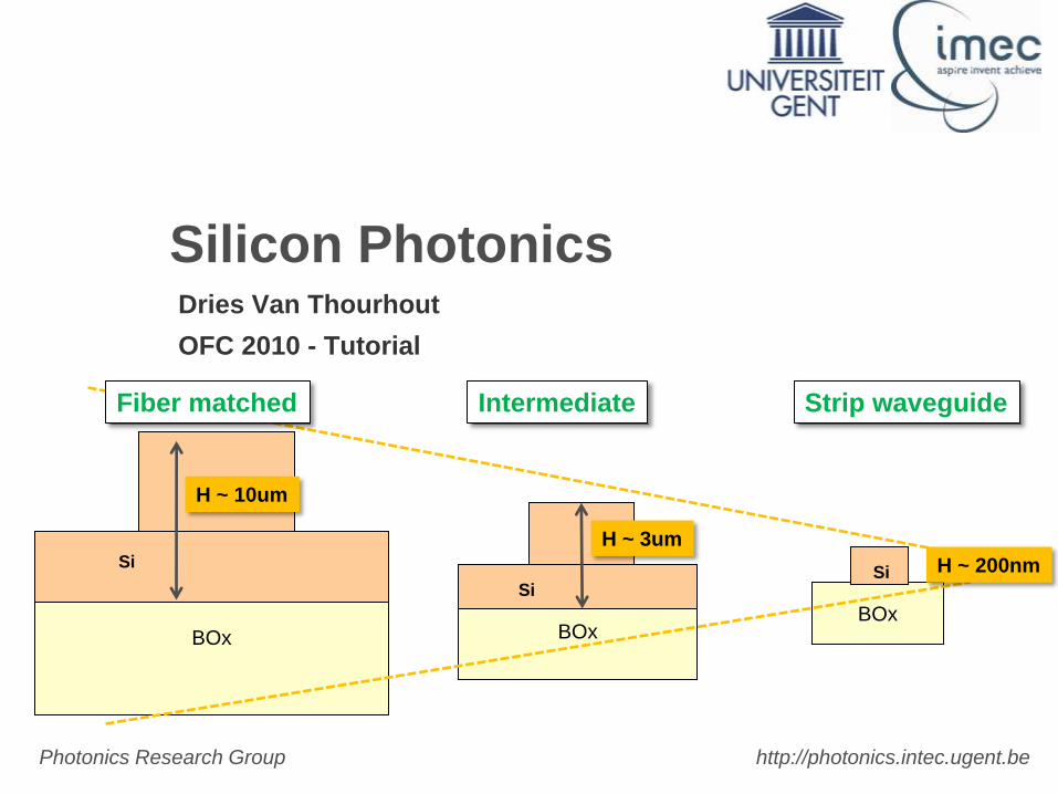
Silicon PhotonicsDries Van Thourhout
OFC 2010 - Tutorial
BOx
Si
H ~ 10um
BOx
Si
BOx
Si
H ~ 3um
H ~ 200nm
Fiber matched Intermediate Strip waveguide
http://photonics.intec.ugent.bePhotonics Research Group
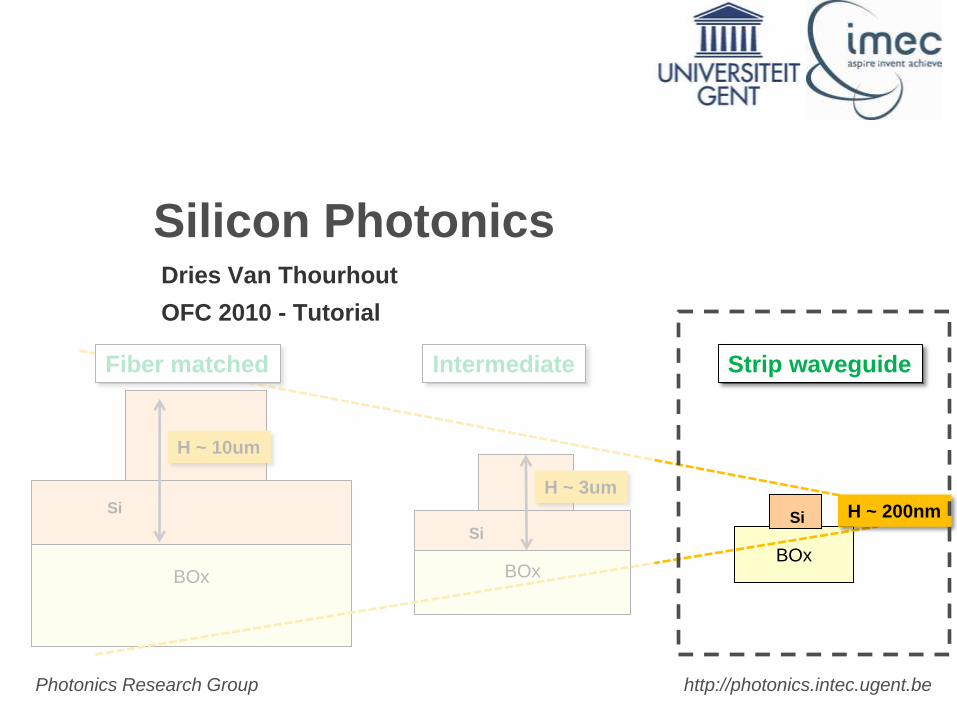
Silicon PhotonicsDries Van Thourhout
OFC 2010 - Tutorial
BOx
Si
H ~ 10um
BOx
Si
BOx
Si
H ~ 3um
H ~ 200nm
Fiber matched Intermediate Strip waveguide
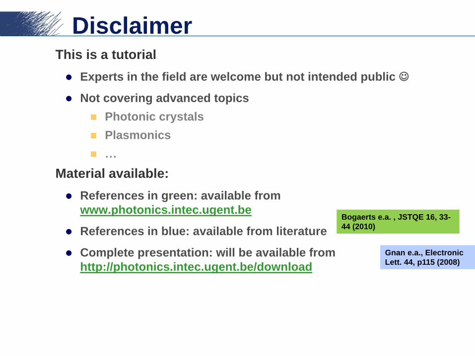
DisclaimerThis is a tutorial
Experts in the field are welcome but not intended public
Not covering advanced topics
Photonic crystals
Plasmonics
…
Material available:
References in green: available from
www.photonics.intec.ugent.be
References in blue: available from literature
Complete presentation: will be available from
http://photonics.intec.ugent.be/download
Bogaerts e.a. , JSTQE 16, 33-
44 (2010)
Gnan e.a., Electronic
Lett. 44, p115 (2008)
http://photonics.intec.ugent.bePhotonics Research Group
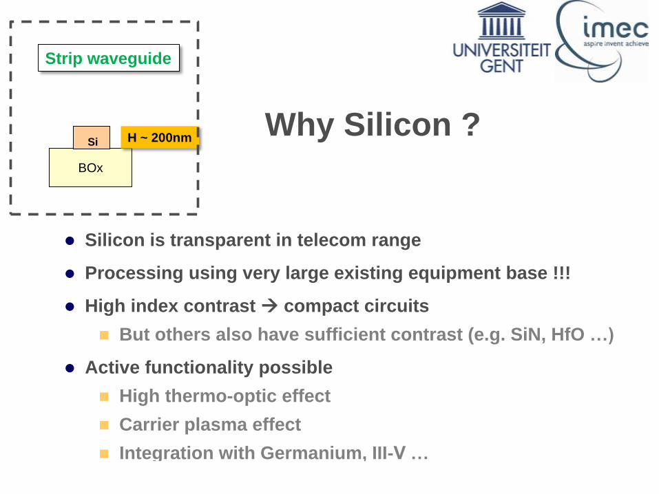
Why Silicon ?
Silicon is transparent in telecom range
Processing using very large existing equipment base !!!
High index contrast compact circuits
But others also have sufficient contrast (e.g. SiN, HfO …)
Active functionality possible
High thermo-optic effect
Carrier plasma effect
Integration with Germanium, III-V …
BOx
Si H ~ 200nm
Strip waveguide
http://photonics.intec.ugent.bePhotonics Research Group
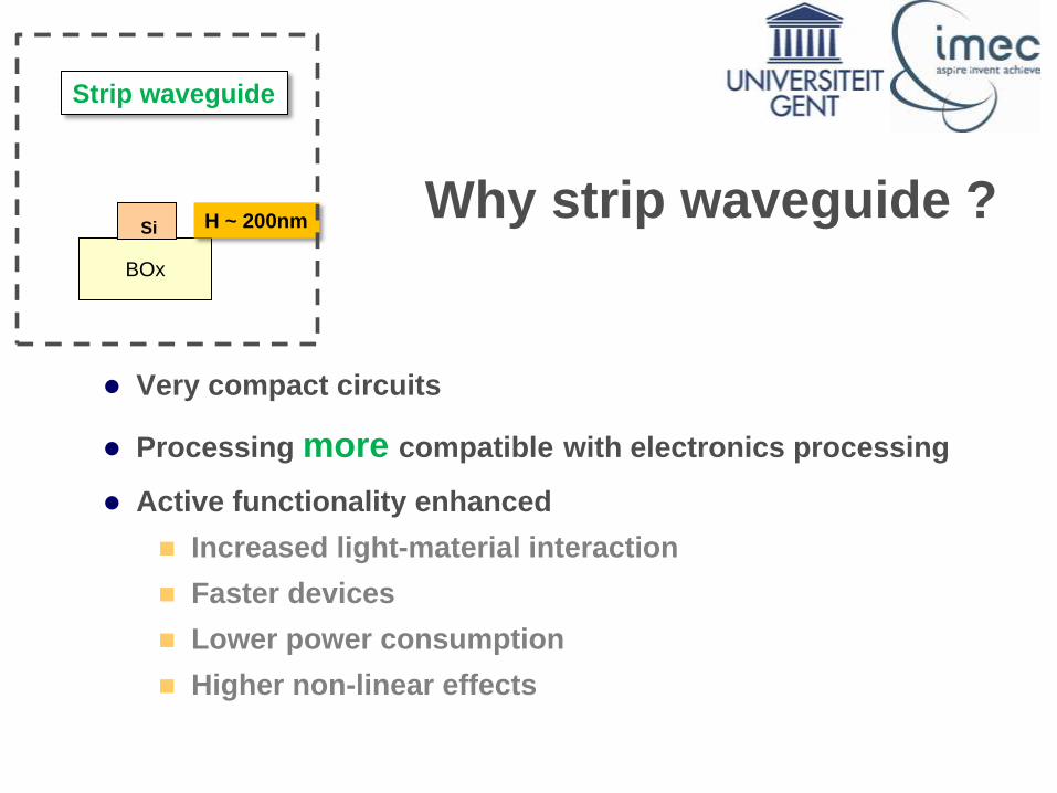
Why strip waveguide ?
Very compact circuits
Processing more compatible with electronics processing
Active functionality enhanced
Increased light-material interaction
Faster devices
Lower power consumption
Higher non-linear effects
BOx
Si H ~ 200nm
Strip waveguide
http://photonics.intec.ugent.bePhotonics Research Group
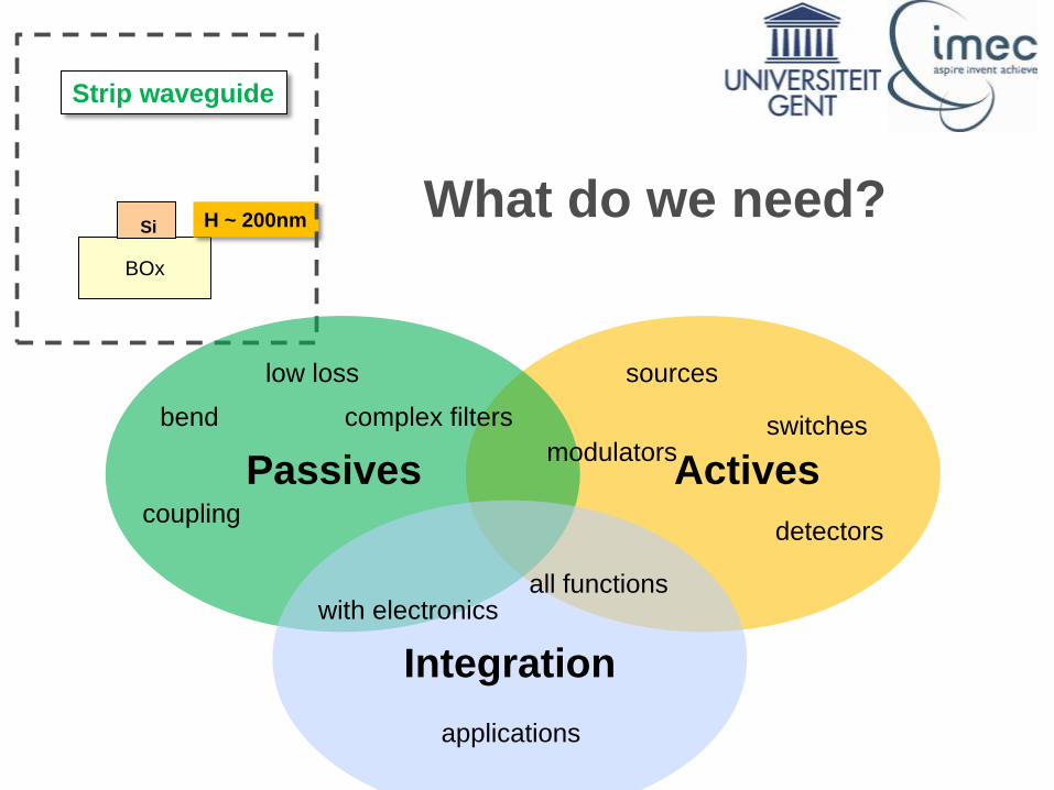
What do we need? BOx
Si H ~ 200nm
Strip waveguide
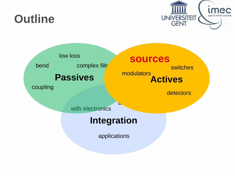
Passives
low loss
bend
coupling
complex filters
Actives
sources
detectors
switchesmodulators
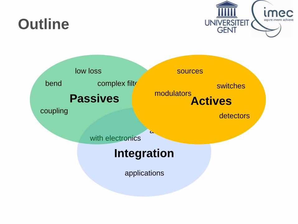
Integration
with electronicsall functions
applications

http://photonics.intec.ugent.bePhotonics Research Group
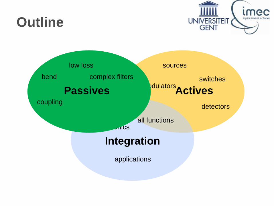
Actives
sources
detectors
switchesmodulators
Integration
with electronicsall functions
applications
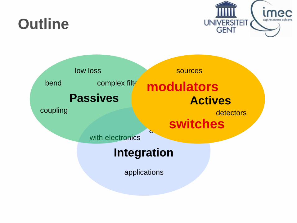
Outline
Passives
low loss
bend
coupling
complex filters
http://photonics.intec.ugent.bePhotonics Research Group
Actives
sources
detectors
switchesmodulators
Integration
with electronicsall functions
applications
Outline
Passives
low loss
bend
coupling
complex filters
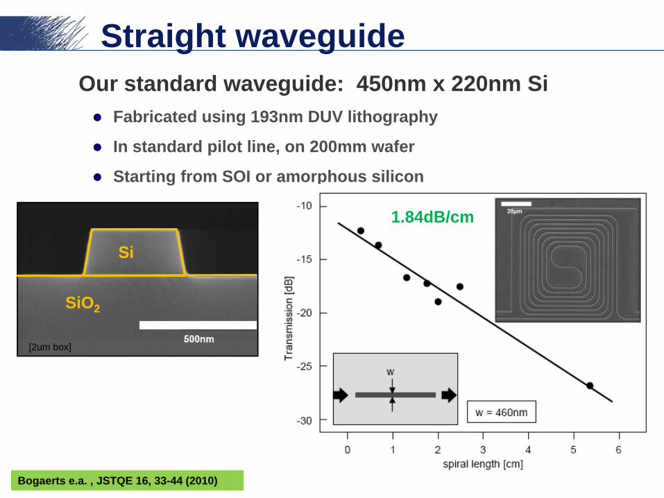
Our standard waveguide: 450nm x 220nm Si
Fabricated using 193nm DUV lithography
In standard pilot line, on 200mm wafer
Starting from SOI or amorphous silicon
Straight waveguide
Si
SiO2
1.84dB/cm
[2um box]
Bogaerts e.a. , JSTQE 16, 33-44 (2010)
Origin of losses ?
Surface roughness
Surface absorption
How to decrease losses further ?
eBEAM lithography + HSQ resist 0.9dB/cm
Surface treatment
Wet or dry oxidation
Hydrogen or other treatment
Encapsulation
Straight waveguide
Gnan e.a., Electronic Lett. 44,
p115 (2008)
Borselli, Painter, e.a., APL 91, 131117 (2007)
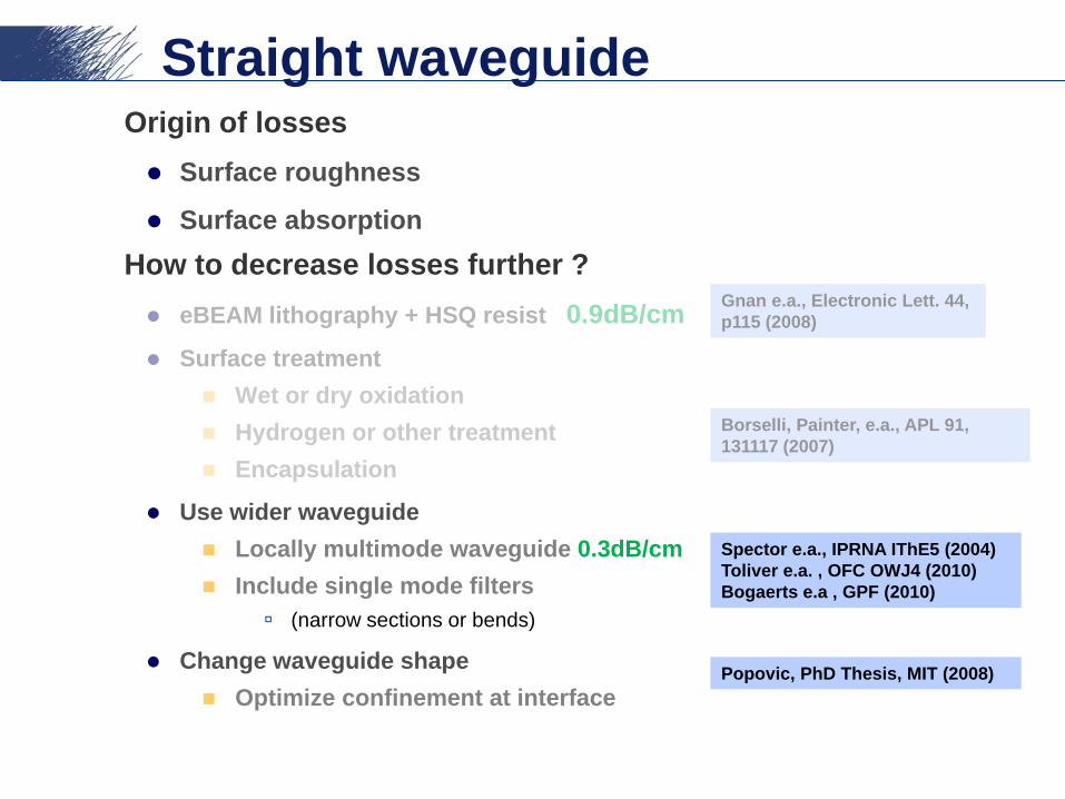
Origin of losses
Surface roughness
Surface absorption
How to decrease losses further ?
eBEAM lithography + HSQ resist 0.9dB/cm
Surface treatment
Wet or dry oxidation
Hydrogen or other treatment
Encapsulation
Use wider waveguide
Locally multimode waveguide 0.3dB/cm
Include single mode filters
(narrow sections or bends)
Change waveguide shape
Optimize confinement at interface
Straight waveguide
Gnan e.a., Electronic Lett. 44,
p115 (2008)
Borselli, Painter, e.a., APL 91,
131117 (2007)
Spector e.a., IPRNA IThE5 (2004)
Toliver e.a. , OFC OWJ4 (2010)
Bogaerts e.a , GPF (2010)
Popovic, PhD Thesis, MIT (2008)
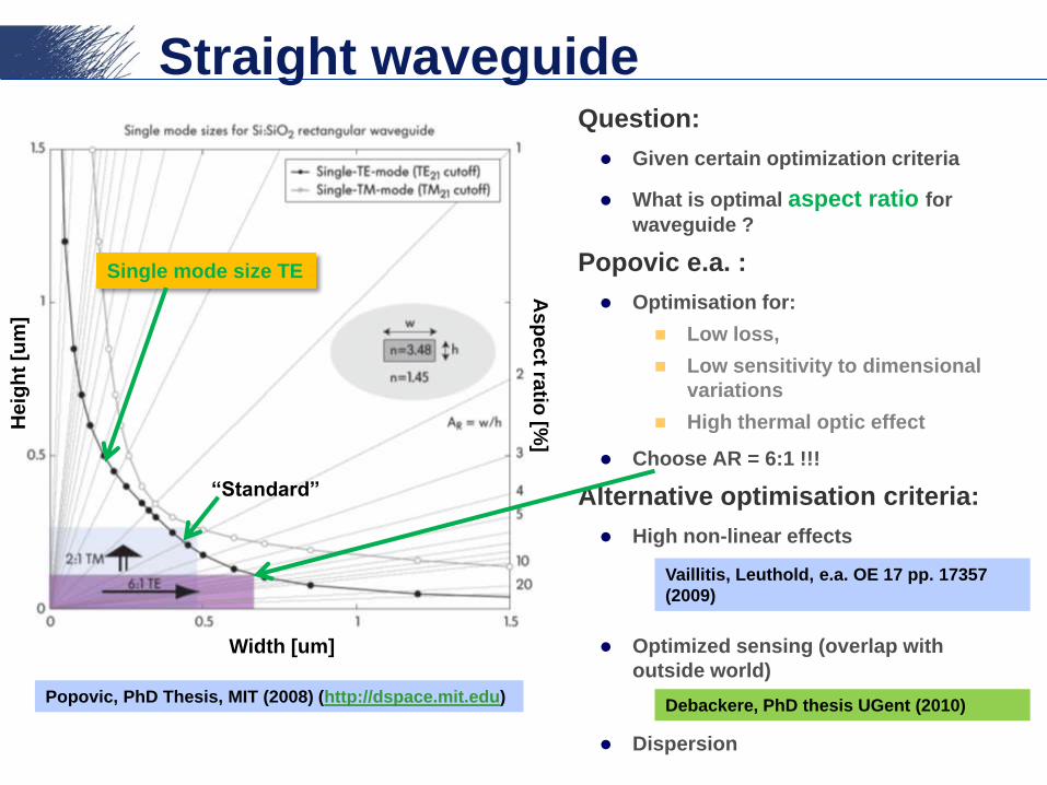
Straight waveguideQuestion:
Given certain optimization criteria
What is optimal aspect ratio for
waveguide ?
Popovic e.a. :
Optimisation for:
Low loss,
Low sensitivity to dimensional
variations
High thermal optic effect
Choose AR = 6:1 !!!
Alternative optimisation criteria:
High non-linear effects
Optimized sensing (overlap with
outside world)
Dispersion
Width [um]
Heig
ht
[um
]
Single mode size TE
Asp
ec
t ratio
[%]
Popovic, PhD Thesis, MIT (2008) (http://dspace.mit.edu)
Vaillitis, Leuthold, e.a. OE 17 pp. 17357
(2009)
Debackere, PhD thesis UGent (2010)
“Standard”

Bend waveguide
Our standard waveguide: 450nm x 220nm Si
Fabricated using 193nm DUV lithography
In standard pilot line, on 200mm wafer
Starting from SOI or amorphous silicon
Si
SiO2
0.02dB/900- In agreement with FDTD calculations
- Offset straigth-bend might improve (?)
S.K. Selvaraja, JLT 27, p.4070 (2009)
Y. A. Vlasov and S. J. McNab, Optics Express, p. 1622 (2004)
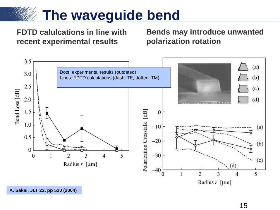
The waveguide bendFDTD calulcations in line with
recent experimental results
Bends may introduce unwanted
polarization rotation
15
Dots: experimental results (outdated)
Lines: FDTD calculations (dash: TE, dotted: TM)
A. Sakai, JLT 22, pp 520 (2004)

Crossings
Standard Crossing
>1dB excess loss
>-10dB crosstalk
Improved version
Not practical !
~0.2dB excess loss
<70dB crosstalk
Bogaerts e.a. , JSTQE 16, 33-44 (2010)

The Y-junction
Example
Simulation: <0.1dB excess loss
Experiment: 0.3dB excess loss
Some imbalance due to opt. Prox.
Sakai e.a., IEICE Trans E85-C 1033 (2002)
Large losses for standard Y-junction
Need improved design !!!
Fukazawa e.a. Jpn JAP 41, p L1461 (2002)
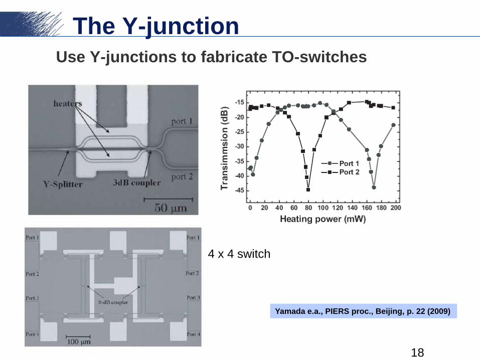
The Y-junction
Use Y-junctions to fabricate TO-switches
18
4 x 4 switch
Yamada e.a., PIERS proc., Beijing, p. 22 (2009)
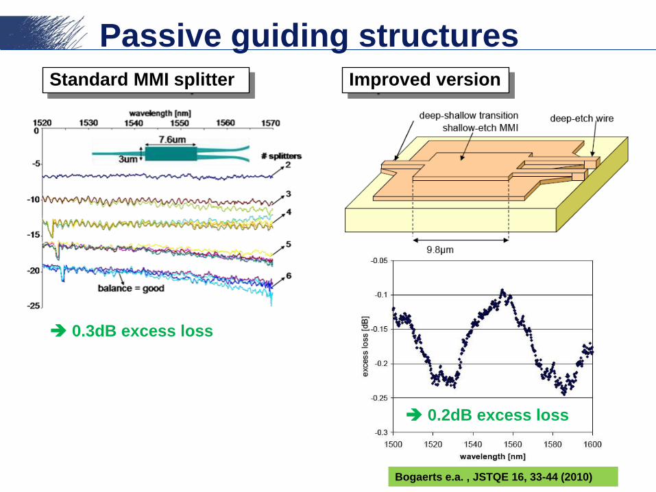
Passive guiding structures
Standard MMI splitter Improved version
0.3dB excess loss
0.2dB excess loss
Bogaerts e.a. , JSTQE 16, 33-44 (2010)
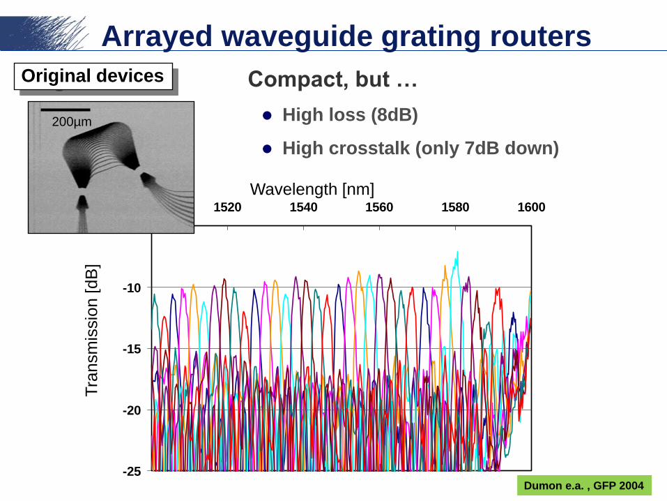
Arrayed waveguide grating routers
Compact, but …
High loss (8dB)
High crosstalk (only 7dB down)
Original devices
-25
-20
-15
-10
-5
1500 1520 1540 1560 1580 1600
Tra
nsm
issio
n [dB
]
Wavelength [nm]
200µm
Dumon e.a. , GFP 2004
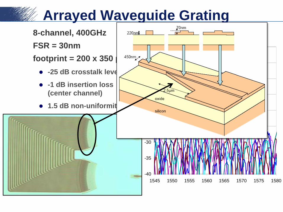
Arrayed Waveguide Grating8-channel, 400GHz
FSR = 30nm
footprint = 200 x 350 µm2
-25 dB crosstalk level
-1 dB insertion loss
(center channel)
1.5 dB non-uniformity
-40
-35
-30
-25
-20
-15
-10
-5
0
1545 1550 1555 1560 1565 1570 1575 1580
Improved devices
Arrayed Waveguide Grating8-channel, 400GHz
FSR = 30nm
footprint = 200 x 350 µm2
-25 dB crosstalk level
-1 dB insertion loss
(center channel)
1.5 dB non-uniformity
-40
-35
-30
-25
-20
-15
-10
-5
0
1545 1550 1555 1560 1565 1570 1575 1580
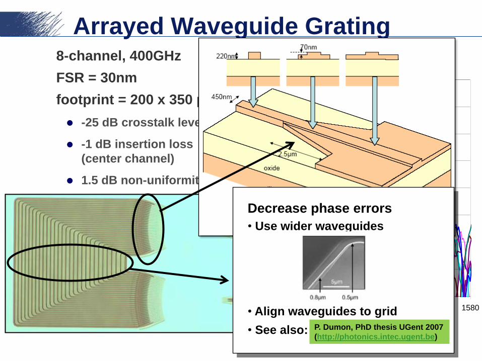
Decrease phase errors
• Use wider waveguides
• Align waveguides to grid
• See also: P. Dumon, PhD thesis UGent 2007
(http://photonics.intec.ugent.be)
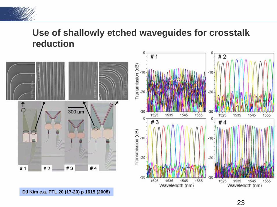
Use of shallowly etched waveguides for crosstalk
reduction
23
DJ Kim e.a. PTL 20 (17-20) p 1615 (2008)
Arrayed Waveguide Grating
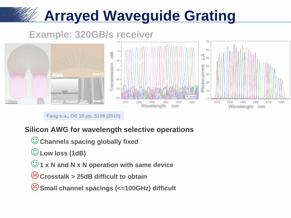
Silicon AWG for wavelength selective operations
Channels spacing globally fixed
Low loss (1dB)
1 x N and N x N operation with same device
Crosstalk > 25dB difficult to obtain
Small channel spacings (<=100GHz) difficult
Example: 320GB/s receiver
Fang e.a., OE 18 pp. 5106 (2010)
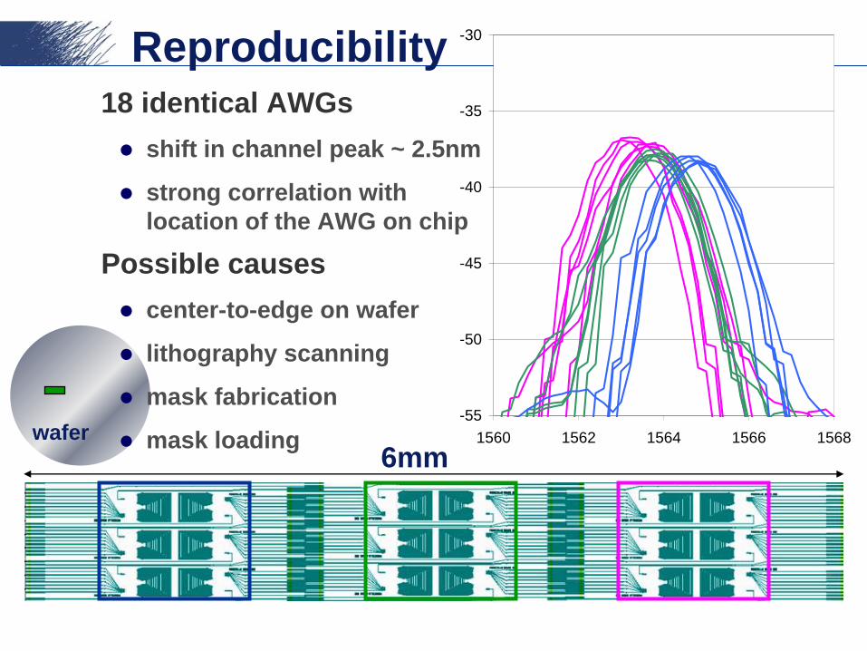
wafer
Reproducibility
18 identical AWGs
shift in channel peak ~ 2.5nm
strong correlation with
location of the AWG on chip
Possible causes
center-to-edge on wafer
lithography scanning
mask fabrication
mask loading6mm
-55
-50
-45
-40
-35
-30
1560 1562 1564 1566 1568
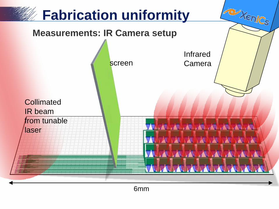
Fabrication uniformity
Measurements: IR Camera setup
6mm
Collimated
IR beam
from tunable
laser
Infrared
Camerascreen
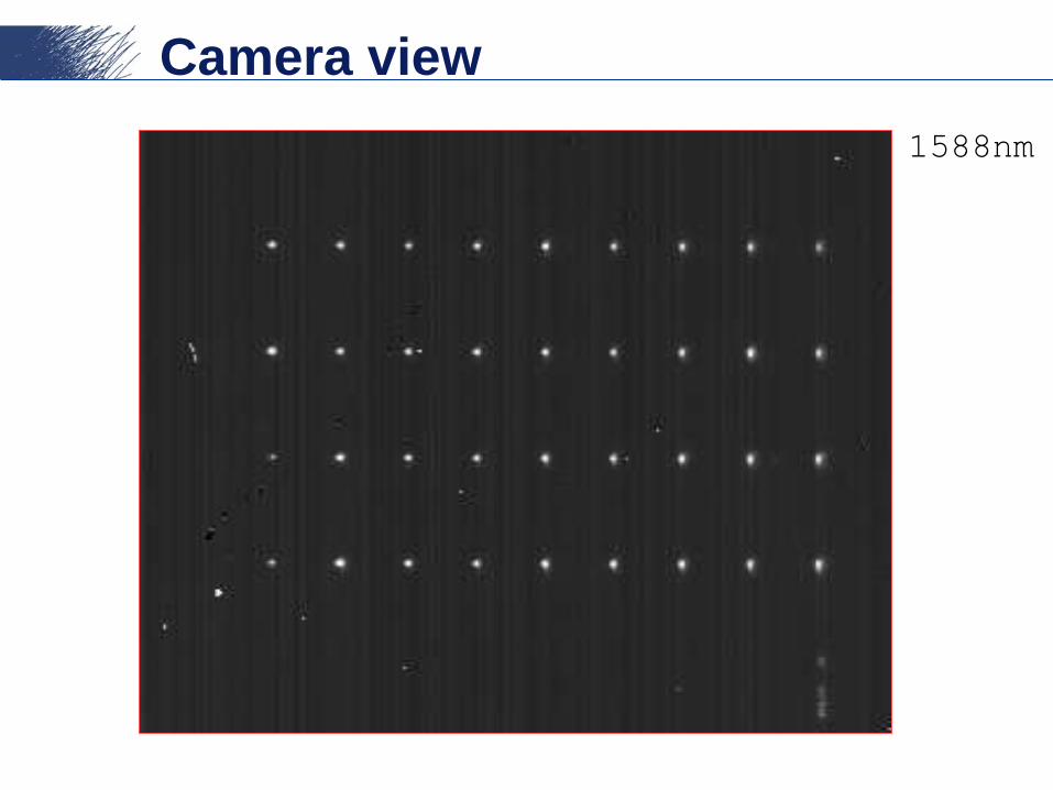
Camera view
1560nm1561nm1562nm1563nm1564nm1565nm1566nm1567nm1568nm1569nm1570nm1571nm1572nm1573nm1574nm1575nm1576nm1577nm1578nm1579nm1580nm1581nm1582nm1583nm1584nm1585nm1586nm1587nm1588nm

Measurements
All rows
0 10 20 301560
1565
1570
1575
1580
1585all channel positions
device#
wavl
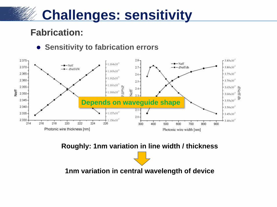
Challenges: sensitivityFabrication:
Sensitivity to fabrication errors
Roughly: 1nm variation in line width / thickness
1nm variation in central wavelength of device
Depends on waveguide shape
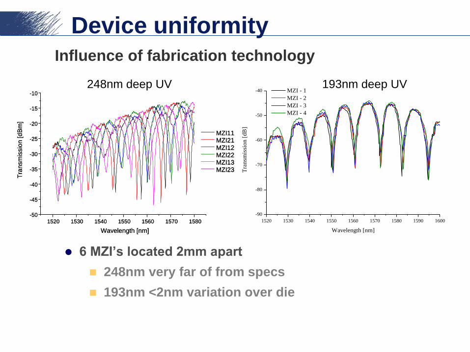
Device uniformity
Influence of fabrication technology
6 MZI’s located 2mm apart
248nm very far of from specs
193nm <2nm variation over die
1520 1530 1540 1550 1560 1570 1580
-50
-45
-40
-35
-30
-25
-20
-15
-10
Tra
nsm
issio
n [
dB
m]
Wavelength [nm]
MZI11MZI21MZI12MZI22MZI13MZI23
1520 1530 1540 1550 1560 1570 1580
-50
-45
-40
-35
-30
-25
-20
-15
-10
Tra
nsm
issio
n [
dB
m]
Wavelength [nm]
MZI11MZI21MZI12MZI22MZI13MZI23
1520 1530 1540 1550 1560 1570 1580 1590 1600
-90
-80
-70
-60
-50
-40
Tra
nsm
issi
on
[d
B]
Wavelength [nm]
MZI - 1
MZI - 2
MZI - 3
MZI - 4
248nm deep UV 193nm deep UV

Wafer Uniformity
Thickness variation over incoming wafer (SOITEC©)
4nm variation within wafer
3nm variation wafer-to-wafer (within lot)
4nm lot-to-lot
Si
SiO2
[2um box]
h
0 2 4 6 8 10 12 14 16 18 20 22 24
0
4
8210
212
214
216
218
220
222
224
226 Within wafer mean
Within wafer stad. deviation
Si th
ickn
ess [
nm
]
# Wafer
3 [
nm
]
0 2 4 6 8 10 12 14 16 18 20 22 24
0
4
8216
218
220
222
224
226
228
230
3 [
nm
]S
i th
ickne
ss [
nm
]
# Wafer
Within wafer mean
Within wafer stad. deviation
Lot A Lot B
(circular within wafer pattern – determined by CMP process)
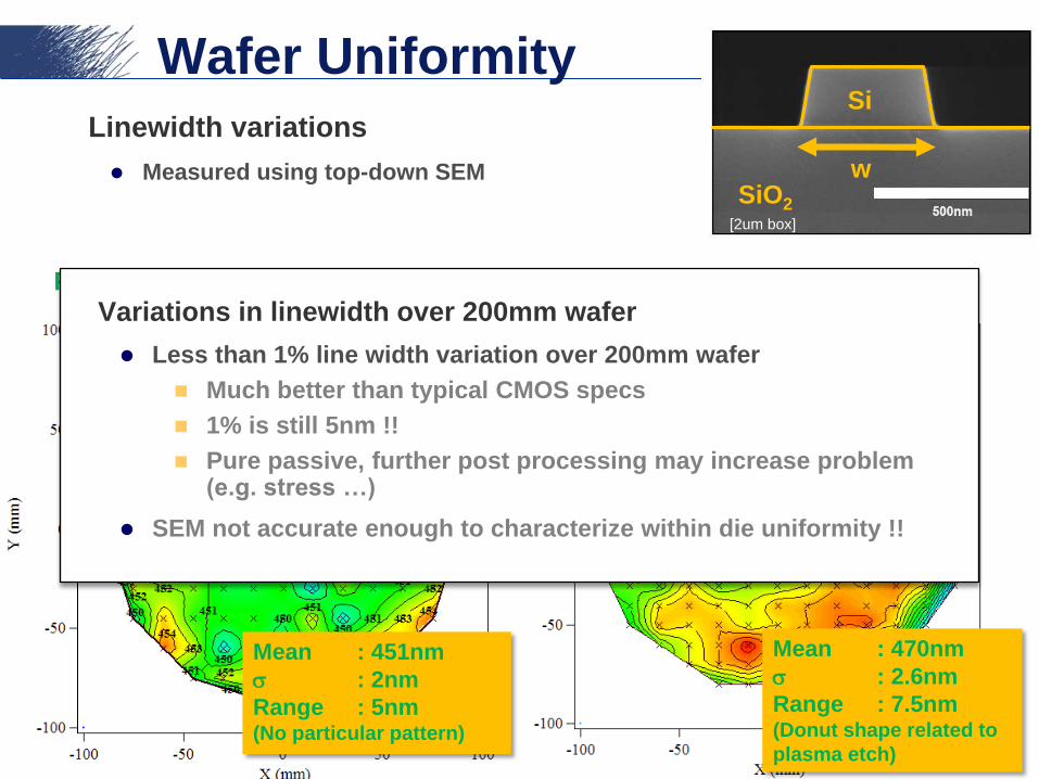
Wafer Uniformity
Linewidth variations
Measured using top-down SEM
Si
SiO2[2um box]
w
Mean : 470nm
: 2.6nm
Range : 7.5nm(Donut shape related to
plasma etch)
Following 193nm DUV lithography Following etching
Mean : 451nm
: 2nm
Range : 5nm(No particular pattern)
Variations in linewidth over 200mm wafer
Less than 1% line width variation over 200mm wafer
Much better than typical CMOS specs
1% is still 5nm !!
Pure passive, further post processing may increase problem (e.g. stress …)
SEM not accurate enough to characterize within die uniformity !!
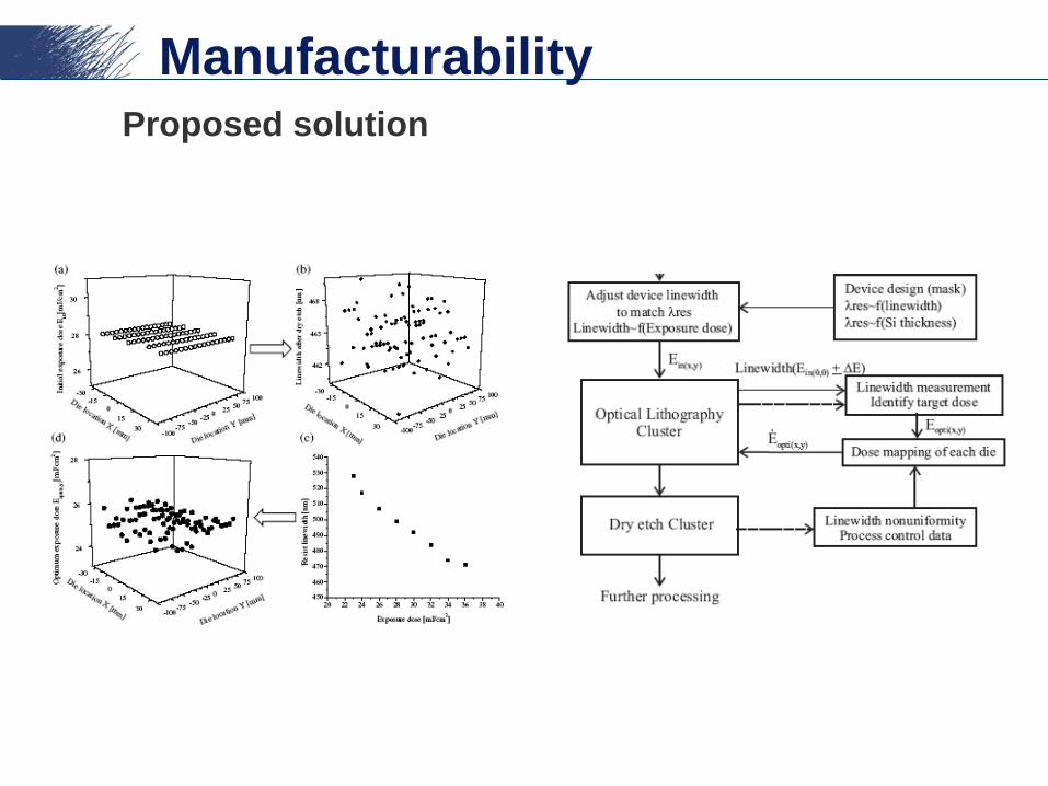
Manufacturability
Proposed solution
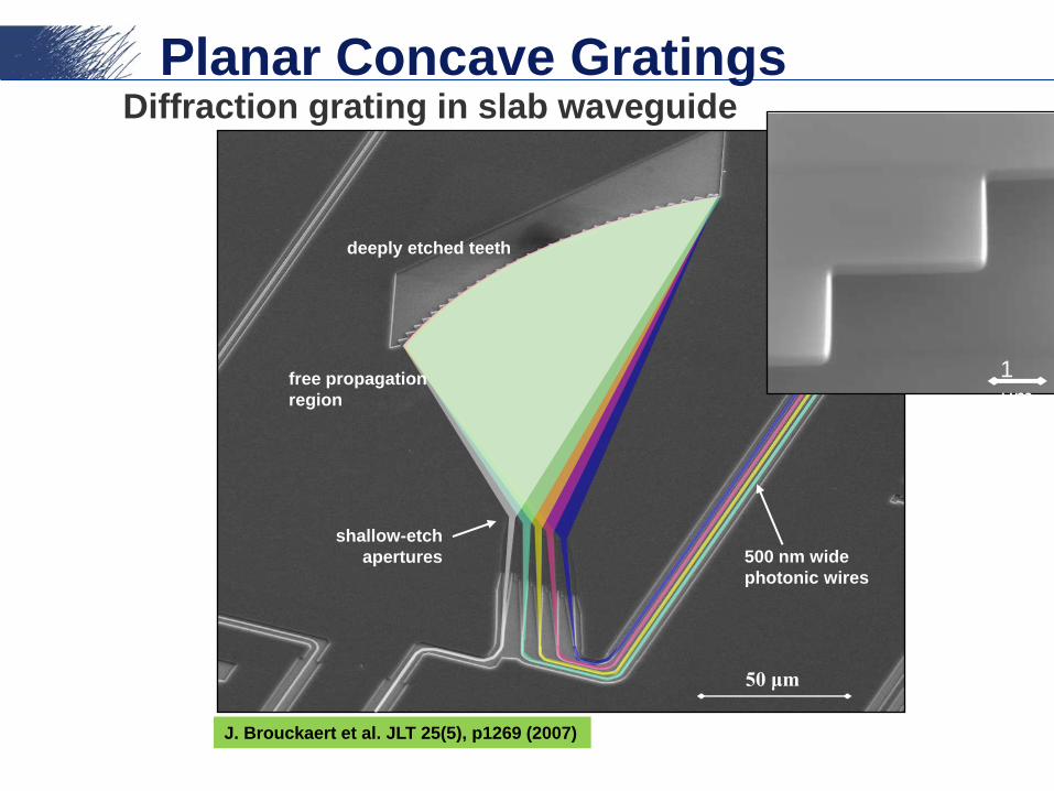
Planar Concave GratingsDiffraction grating in slab waveguide
free propagation
region
50 μm
shallow-etch
apertures 500 nm wide
photonic wires
1
μm
deeply etched teeth
J. Brouckaert et al. JLT 25(5), p1269 (2007)
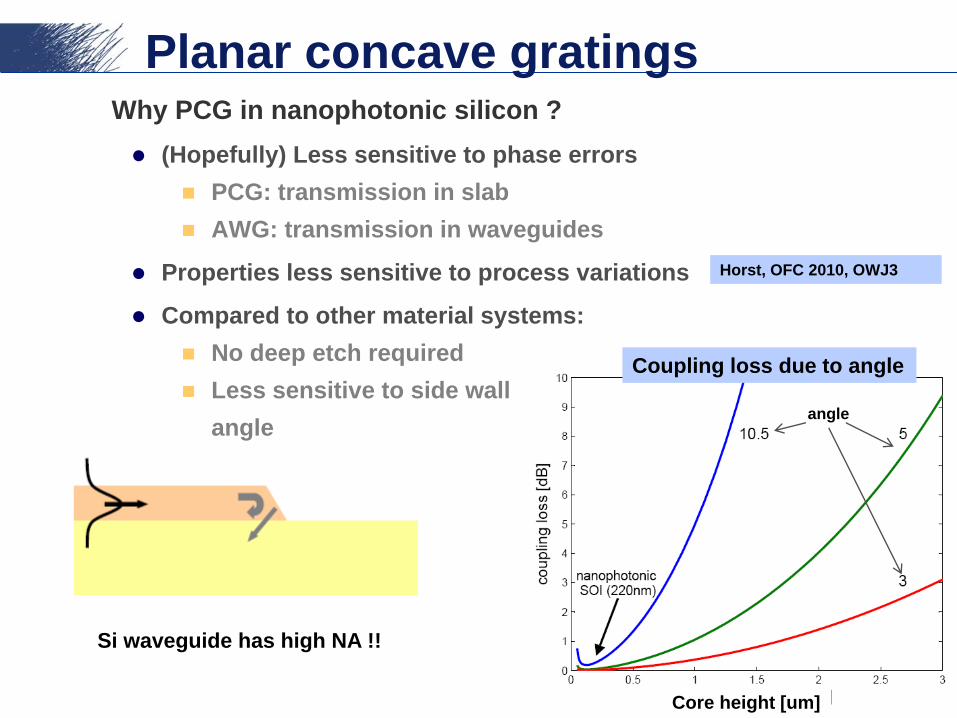
Planar concave gratingsWhy PCG in nanophotonic silicon ?
(Hopefully) Less sensitive to phase errors
PCG: transmission in slab
AWG: transmission in waveguides
Properties less sensitive to process variations
Compared to other material systems:
No deep etch required
Less sensitive to side wall
angle
Coupling loss due to angle
angle
Core height [um]
Si waveguide has high NA !!
Horst, OFC 2010, OWJ3
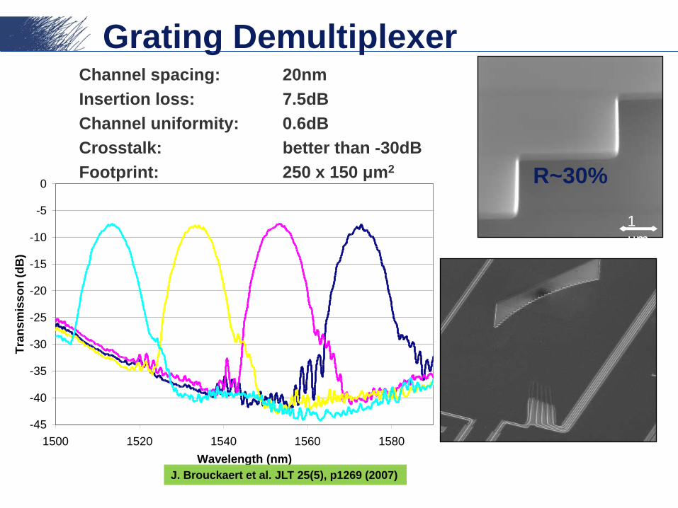
Grating DemultiplexerChannel spacing: 20nm
Insertion loss: 7.5dB
Channel uniformity: 0.6dB
Crosstalk: better than -30dB
Footprint: 250 x 150 μm2
-45
-40
-35
-30
-25
-20
-15
-10
-5
0
1500 1520 1540 1560 1580
Wavelength (nm)
Tra
nsm
iss
on
(d
B)
1
μm
R~30%
J. Brouckaert et al. JLT 25(5), p1269 (2007)

Grating DemultiplexerHigh Fresnel reflection loss at grating ?
Use metal coating
Use DBR mirror
Use TIR mirror
DBR-mirror
TIR-mirror
Horst e.a., PTL 21, pp 1743 (2009)
See also: Horst, OFC 2010, OWJ3 (invited)J. Brouckaert et al. PTL 20(4), p309 (2008)
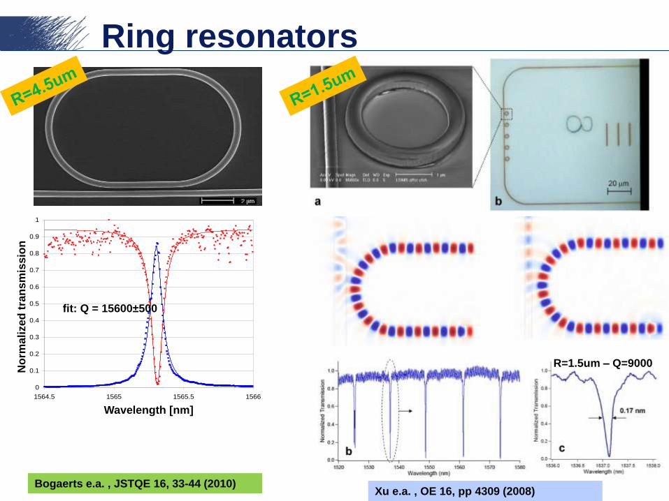
Ring resonators
0
0.1
0.2
0.3
0.4
0.5
0.6
0.7
0.8
0.9
1
1564.5 1565 1565.5 1566
Wavelength [nm]
No
rmalized
tran
sm
iss
ion
fit: Q = 15600±500
Bogaerts e.a. , JSTQE 16, 33-44 (2010)Xu e.a. , OE 16, pp 4309 (2008)
R=1.5um – Q=9000
Ring resonators for sensing
-0.1
0
0.1
0.2
0.3
0.4
0.5
0.6
0 20 40 60 80 100 120
wa
vele
ng
th s
hif
t [n
m]
time [min]
Serum with anti-HuIgG Serum with anti-HSA
HuIgG - αHuIgG
HSA - αHSA
BSA receptor
no receptor
Devos e.a., IEEE Photonics Journal, 1(4), p.225-235 (2009)
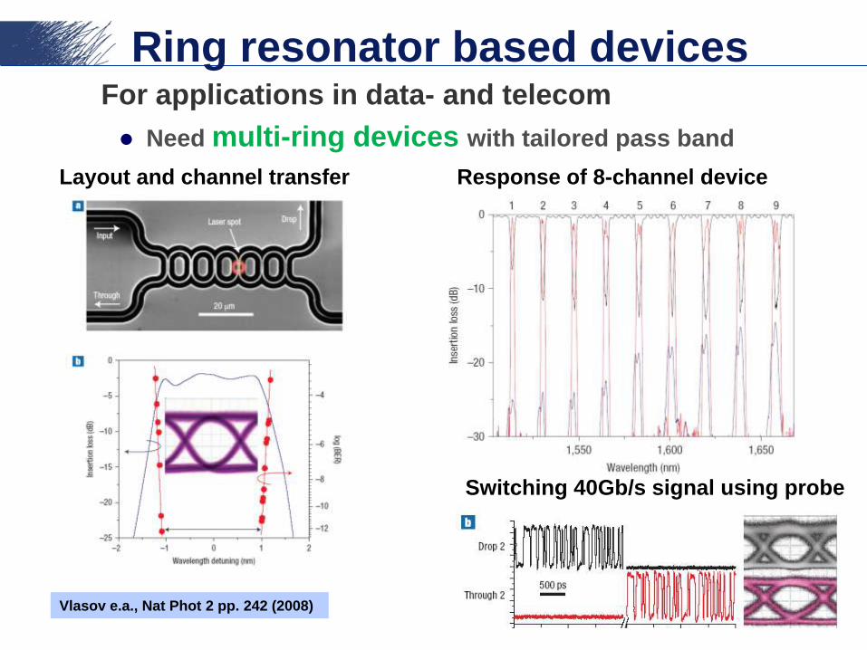
Ring resonator based devicesFor applications in data- and telecom
Need multi-ring devices with tailored pass band
Vlasov e.a., Nat Phot 2 pp. 242 (2008)
Response of 8-channel device
Switching 40Gb/s signal using probe
Layout and channel transfer

Ring resonators
Ring resonators for label extractor
EU-project BOOM
Need 0.1nm bandwidth filter
Use silicon ring resonator ??
Label extractor
Wavelength conversion
Tunable laser
Tuning current

TE-Microring meeting BOOM specs? NO
R = 20um, gap = 400nm
Ring resonators conclusionTE ring resonators
Very sensitive to random back scattering
Behaviour very unpredictable
High losses
TM ring resonators ?

TM-Microring meeting BOOM specs? YES !
R = 20um, gap = 1um

Ring resonators conclusionTE ring resonators
Very sensitive to random back scattering
Behaviour very unpredictable
High losses
TM ring resonators
Lower confinement at side walls
Lower loss, lower back scattering
Record high Q values demonstrated (Qi=340.000)
DeHeyn e.a. , submitted to OFC 2011
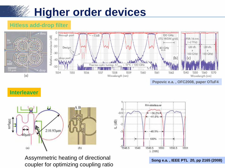
Higher order devices
Popovic e.a. , OFC2008, paper OTuF4
Hitless add-drop filter
Interleaver
Song e.a. , IEEE PTL 20, pp 2165 (2008)Assymmetric heating of directional
coupler for optimizing coupling ratio
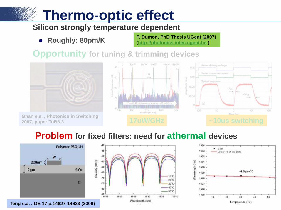
Thermo-optic effectSilicon strongly temperature dependent
Roughly: 80pm/K
Opportunity for tuning & trimming devices
P. Dumon, PhD Thesis UGent (2007)
(http://photonics.intec.ugent.be )
Gnan e.a. , Photonics in Switching
2007, paper TuB3.3 17uW/GHz ~10us switching
Problem for fixed filters: need for athermal devices
Teng e.a. , OE 17 p.14627-14633 (2009)
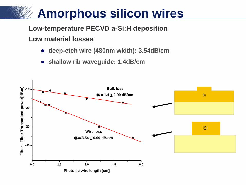
Amorphous silicon wires Low-temperature PECVD a-Si:H deposition
Low material losses
deep-etch wire (480nm width): 3.54dB/cm
shallow rib waveguide: 1.4dB/cm
0.0 1.5 3.0 4.5 6.0
-40
-30
-20
-10
Wire loss
3.54 + 0.09 dB/cm
Bulk loss
1.4 + 0.09 dB/cm
Fib
er
- F
ibe
r T
ran
sm
ite
d p
ow
er[
dB
m]
Photonic wire length [cm]

Amorphous silicon wires Amorphous silicon
Shows improved non-linear performance
Lower non-linear absorption
Higher non-linear n2
Demonstrated 26dB parametric gain (on-chip)
Results presented at IEEE Photonics
Society annual meeting (Denver, 2010)
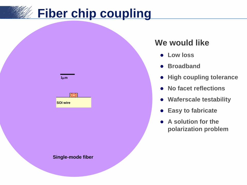
Fiber chip coupling
Single-mode fiber
1mm
SOI wire
We would like
Low loss
Broadband
High coupling tolerance
No facet reflections
Waferscale testability
Easy to fabricate
A solution for the
polarization problem
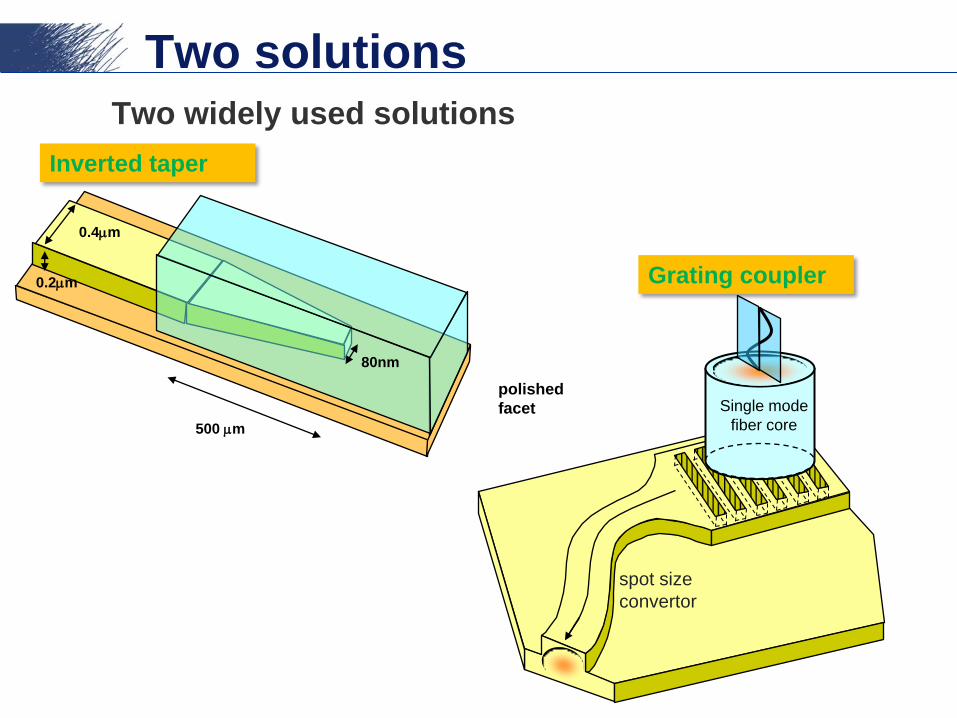
Two solutions
Two widely used solutions
0.4mm
80nm
0.2mm
500 mm
polished
facet
Inverted taper
Grating coupler
spot size
convertor
Single mode
fiber core
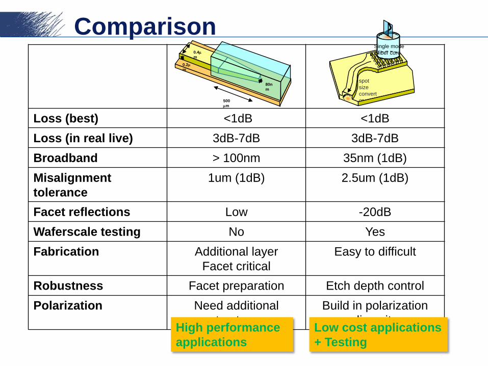
Comparison
Loss (best) <1dB <1dB
Loss (in real live) 3dB-7dB 3dB-7dB
Broadband > 100nm 35nm (1dB)
Misalignment
tolerance
1um (1dB) 2.5um (1dB)
Facet reflections Low -20dB
Waferscale testing No Yes
Fabrication Additional layer
Facet critical
Easy to difficult
Robustness Facet preparation Etch depth control
Polarization Need additional
structures
Build in polarization
diversity
spot
size
convert
or
Single mode
fiber core0.4m
m
80n
m
0.2m
m
500
mm
High performance
applications
Low cost applications
+ Testing
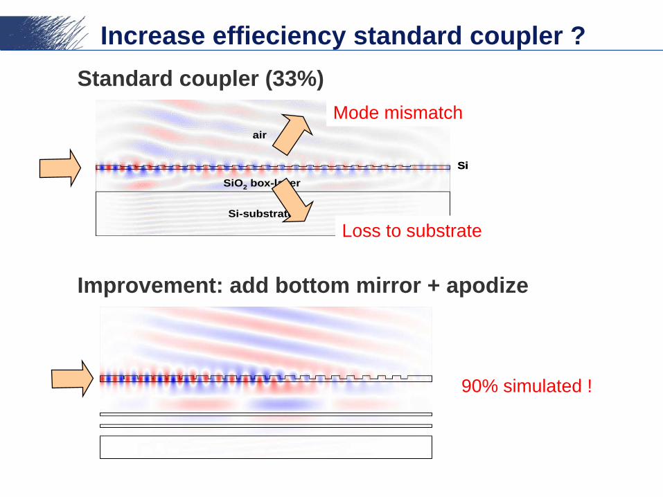
Increase effieciency standard coupler ?
Standard coupler (33%)
Improvement: add bottom mirror + apodize
air
Si
SiO2 box-layer
Si-substrate
air
Si
SiO2 box-layer
Si-substrate
Mode mismatch
Loss to substrate
90% simulated !
Gratings with bottom mirror
Buffer Silicon dioxide DBR mirror
Grating fiber coupler in a-Si:H
Isolation Silicon dioxide
Poly Si SiO2
Poly Si
DBR bottom mirror• Poly silicon DBR mirror
• a-Si waveguides
Gold bottom mirror• Use waferbonding
• c-Si waveguides
Selvaraja et al. CLEO/IQEC 2009
6.4 %
Van Laere et al., JLT 25(1), p.151 (2007)
69% coupling efficiency

-5.0
-4.5
-4.0
-3.5
-3.0
-2.5
-2.0
-1.5
-1.0
-0.5
0.0
1510 1520 1530 1540 1550 1560 1570
Inse
rtio
n lo
ss f
or
1 c
ou
ple
r [d
B]
Wavelength [nm]
Overlay gratings
Break top-bottom symmetry
2µm SiO2
silicon substrate
220nm Si
380nm teeth
68% coupling efficiency

Grating zoo
Focusing grating
F. Van Laere, PTL 19, p. 1919 (2006)
Metal gratings
Scheerlinck, APL 92 p.031104 (2008)
Polymer wedge for
vertical coupling
Schrauwen e.a.Phot.
West, 7218, , p.72180B (2009)
Photonic crystal grating for low
reflection deep etch
Liu e.a. , OFC2010, paper OWJ2
Apodized grating
Tang e.a. , OFC2010, paper OWJ6

TE/TM interaction
TE-polarization
TE-polarization
Waveguide width [um]
Effective
index

TE/TM interaction
AnticrossingsTM-polarization
TM-polarization
Waveguide width [um]
Effective
index
Solution:• Use SiO2 cover or index matching oil
• Vermeulen e.a. , ECIO 2010

Polarization diversity
Process both polarizations separately
split polarizations
convert to the same polarization on the chip
combine polarization back into the fiber
two
identical
circuits
TE/TM
TMTE
TETM
TE/TM TE/TM

Polarization diversity
Polarization diversity with inverted taper
Need on-chip polarization splitter + rotator
TE/TM
TM
TETE
Watts et al, OL 30(9), p.937 (2005)
Coupling length TM << TE
Fukuda e.a., OE 14(25), p. 12401 (2006)

Polarization diversityPolarization diversity with inverted taper Need on-chip polarization splitter + rotator
Vermeulen e.a. GPF 2010, paper WC6
Polarization conversion efficiency
See also: Wang & Dai, JOSA B, pp. 747-753 (2008)
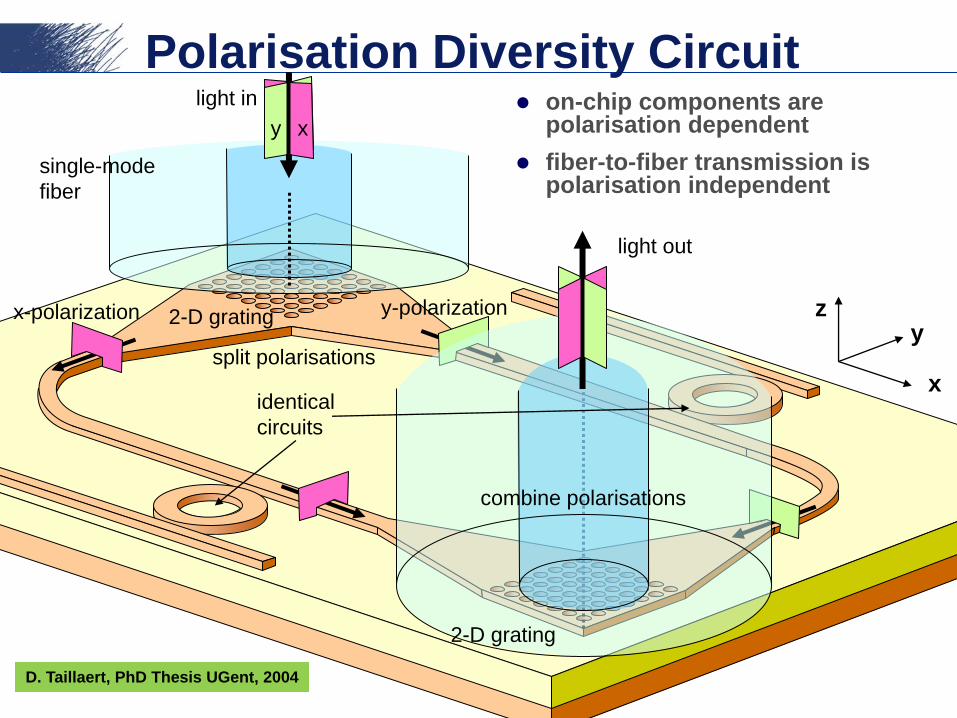
on-chip components are polarisation dependent
fiber-to-fiber transmission is polarisation independent
Polarisation Diversity Circuit
y-polarization
split polarisations
light in
identical
circuits
x-polarization
x
yz
xy
light out
single-mode
fiber
2-D grating
combine polarisations
2-D grating
D. Taillaert, PhD Thesis UGent, 2004
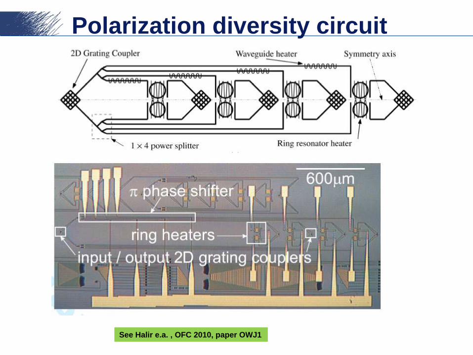
Polarization diversity circuit
See Halir e.a. , OFC 2010, paper OWJ1

What we did not cover in passives
Details of fabrication
Special waveguides
Slot waveguides
Photonic crystal waveguides
Non linearities
Interesting science
But also: big headache
And much more …
S.K. Selvaraja, JLT 27, p.4070 (2009)
http://photonics.intec.ugent.bePhotonics Research Group
Integration
with electronicsall functions
applications
Outline
Passives
low loss
bend
coupling
complex filters
Actives
sources
detectors
switchesmodulators

http://photonics.intec.ugent.bePhotonics Research Group
Integration
with electronicsall functions
applications
Outline
Passives
low loss
bend
coupling
complex filters
Actives
sources
detectors
switchesmodulators
Detector
1. Hybrid integration
Prefabricated diode,
E.g. flip-chip on top of grating coupler
Cost effective for low density, medium speed
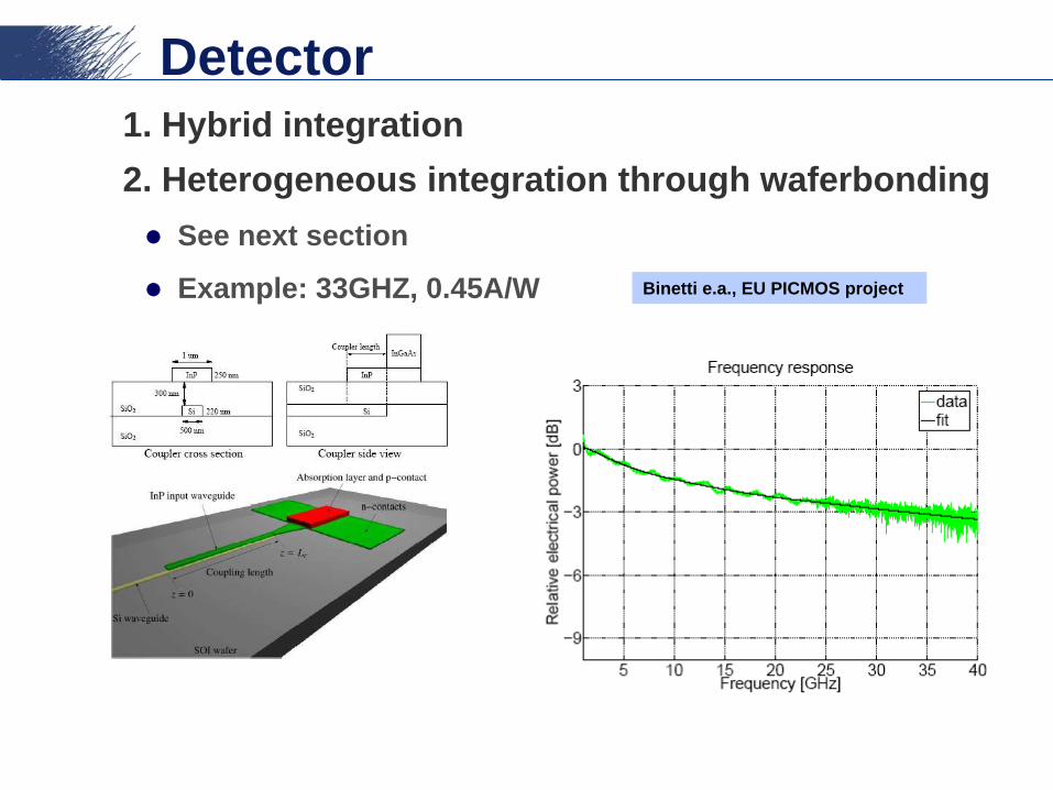
Detector
1. Hybrid integration
2. Heterogeneous integration through waferbonding
See next section
Example: 33GHZ, 0.45A/W Binetti e.a., EU PICMOS project
Detector
1. Hybrid integration
2. Heterogeneous integration through waferbonding
3. Implanted silicon, silicides …
Low efficiency + slow
Easy to process
Useful monitor
Kotura, OFC2010, Monday

Detector
1. Hybrid integration
2. Heterogeneous integration through waferbonding
3. Implanted silicon, silicides …
4. Germanium
Efficient absorber up to 1600nm
Large lattice mismatch (~4%). How to integrate ?
Buffer layer ? Requires 1-10um : Too thick !!
Two step growth process
Rapid melt growth

Ge-epitaxyTwo-step growth process:
Direct growth of Ge on Si at low temperature ( ~350°) CVD
Thin (a few 10nm) highly-dislocated Ge layer
Growth of thick Ge layer (few 100nm) at high temperature (~600°)
High quality Ge absorbing layer
Thermal annealing to reduce the dislocation density
Using MBE, UHV-CVD, RP-CVD …
BOx
Si
LT Ge (~350C, ~50nm)
HT Ge (~600C, 300-500nm)

Ge-epitaxyTwo-step growth process:
Direct growth of Ge on Si at low temperature ( ~350°) CVD
Thin (a few 10nm) highly-dislocated Ge layer
Growth of thick Ge layer (few 100nm) at high temperature (~600°)
High quality Ge absorbing layer
Thermal annealing to reduce the dislocation density
Using MBE, UHV-CVD, RP-CVD …
Different integration approaches:
BOx
Si
Butt Coupling
BOx
Si
Evanescent Coupling
BOx
Si
Two level

Ge-detector
Two step growth – butt coupling
Vivien e.a. , OE 17, pp. 6252 (2009)

Ge-detectorRapid melt growth
1. Ge CVD deposition on SiON mask with small opening
2. Encapsulation
3. RTA induces melt + recristallisation to single crystal
Assefa e.a. , OE 18, pp4997 (2010)
Assefa e.a. , Nature (2010)
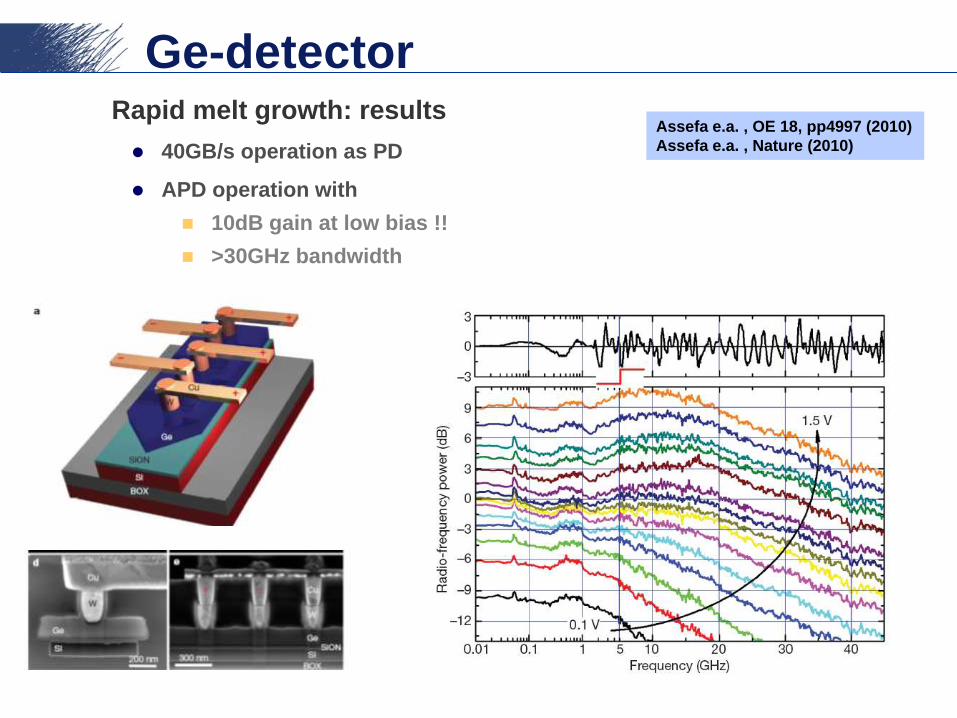
Ge-detectorRapid melt growth: results
40GB/s operation as PD
APD operation with
10dB gain at low bias !!
>30GHz bandwidth
Assefa e.a. , OE 18, pp4997 (2010)
Assefa e.a. , Nature (2010)
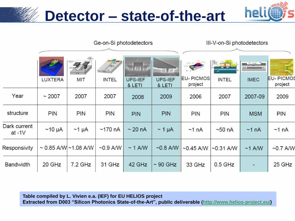
Detector – state-of-the-art
Table compiled by L. Vivien e.a. (IEF) for EU HELIOS project
Extracted from D003 “Silicon Photonics State-of-the-Art”, public deliverable (http://www.helios-project.eu/)
http://photonics.intec.ugent.bePhotonics Research Group
Integration
with electronicsall functions
applications
Outline
Passives
low loss
bend
coupling
complex filters
Actives
sources
detectors
switches
modulators

Modulation of lightHow to make a modulator in silicon
Silicon has no intrinsic EO-effect
But:
Free carriers induce absorption
And index modulation …
Empiric relations determined
Change carrier densities by
Doping
Injection/extraction of carriers
Soref , JQE 23, (1987).
Plasma dispersion
effect
(in silicon at 1550nm –
carrier densities in cm-3)
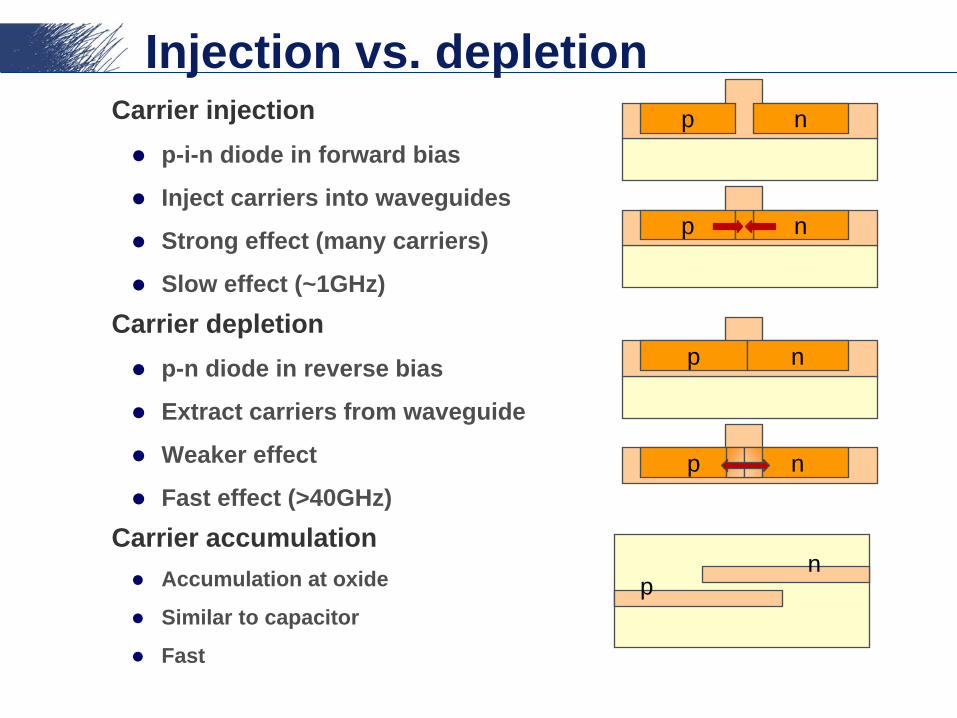
Injection vs. depletionCarrier injection
p-i-n diode in forward bias
Inject carriers into waveguides
Strong effect (many carriers)
Slow effect (~1GHz)
Carrier depletion
p-n diode in reverse bias
Extract carriers from waveguide
Weaker effect
Fast effect (>40GHz)
Carrier accumulation
Accumulation at oxide
Similar to capacitor
Fast
p n
p n
p n
p n
pn
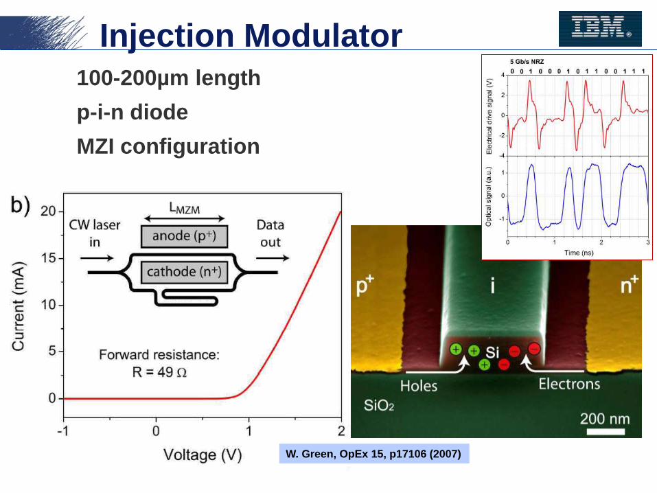
Injection Modulator
100-200µm length
p-i-n diode
MZI configuration
W. Green, OpEx 15, p17106 (2007)
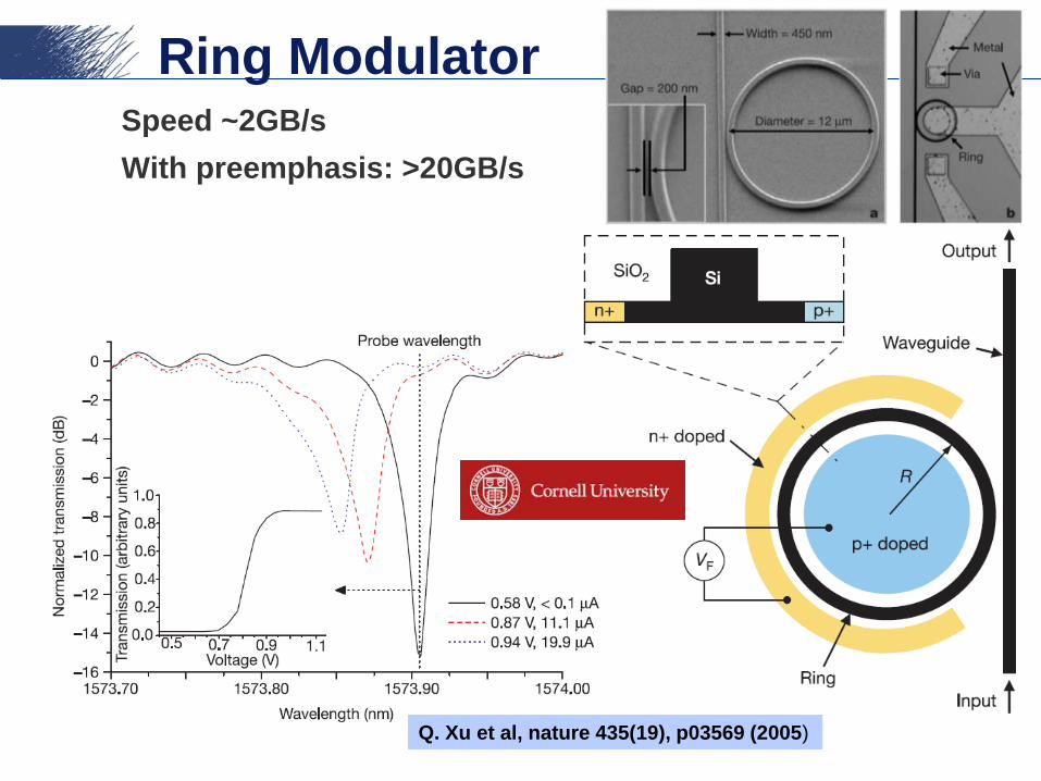
Ring ModulatorSpeed ~2GB/s
With preemphasis: >20GB/s
Q. Xu et al, nature 435(19), p03569 (2005)

Example: depletion modulator
Complex multi-doping profile
Larger index change
Lower RC
But
Still a long device (4mm)
Requires travelling wave electrodes
D. Marris-Morini, OpEx 16 (2008)
4mm long mach zehnder
signal
phase shifter
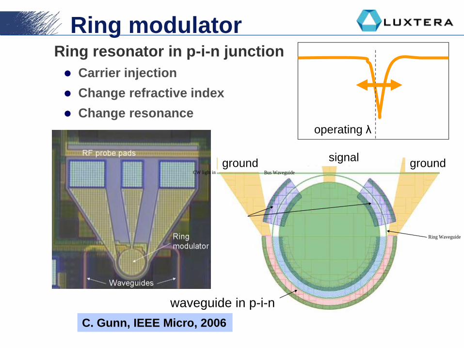
Ring modulatorRing resonator in p-i-n junction
Carrier injection
Change refractive index
Change resonance
Bus Waveguide
Ring Waveguide
High-speed modulation region
(pn diode)
High-speed electrical signalGround Ground
CW light in
groundsignal
ground
waveguide in p-i-n
operating λ
C. Gunn, IEEE Micro, 2006
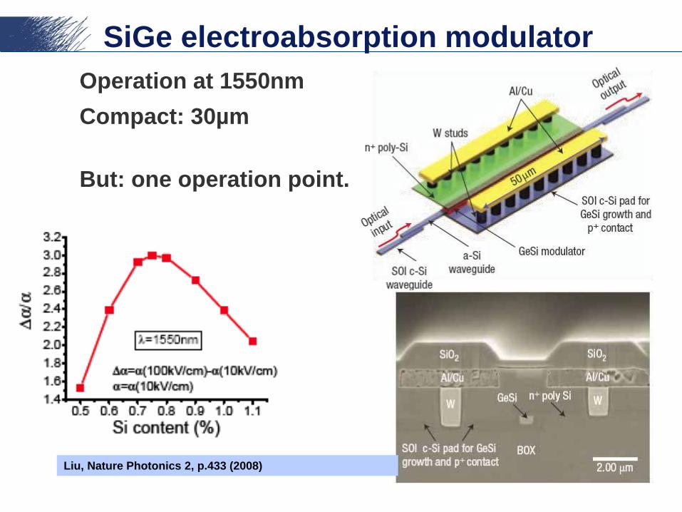
SiGe electroabsorption modulator
Operation at 1550nm
Compact: 30µm
But: one operation point.
Liu, Nature Photonics 2, p.433 (2008)
http://photonics.intec.ugent.bePhotonics Research Group
Integration
with electronicsall functions
applications
Outline
Passives
low loss
bend
coupling
complex filters
Actives
sources
detectors
switchesmodulators

Sources on Silicon
1. Hybrid integration
Song e.a. OE 17, 14063-14068 (2009).

Sources on Silicon
1. Hybrid integration
2. Monolithic integration
MIT press release
Strained Ge-laser Er-doped Si nanocrystals
Zhizhong, Y. et al. Proc of the
IEEE 97, 1250 (2009).
III-V on silicon epitaxy
Junesand e.a., IPRM 2009 pp59

Sources on Silicon
1. Hybrid integration
2. Monolithic integration
3. Integration through waferbonding techniques
(a) (b)
(e) (f)
(c)
(d)
SOI-wafer Planarization Bonding
Substrate Removal Pattern definition III-V processing
III-V/Silicon photonics
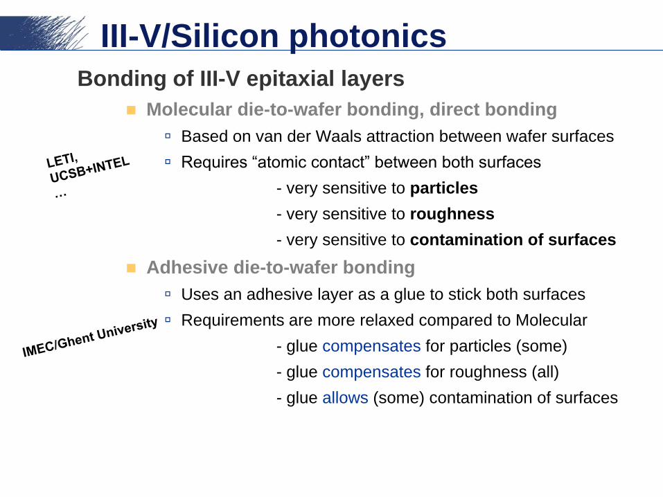
Bonding of III-V epitaxial layers
Molecular die-to-wafer bonding, direct bonding
Based on van der Waals attraction between wafer surfaces
Requires “atomic contact” between both surfaces
- very sensitive to particles
- very sensitive to roughness
- very sensitive to contamination of surfaces
Adhesive die-to-wafer bonding
Uses an adhesive layer as a glue to stick both surfaces
Requirements are more relaxed compared to Molecular
- glue compensates for particles (some)
- glue compensates for roughness (all)
- glue allows (some) contamination of surfaces
© intec 2009 - Photonics Research Group - http://photonics.intec.ugent.be
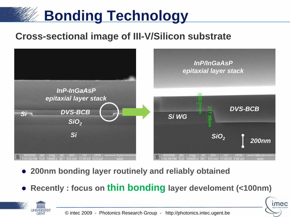
Bonding Technology
200nm
Cross-sectional image of III-V/Silicon substrate
InP-InGaAsP
epitaxial layer stack
DVS-BCB
SiO2
Si
Si Si WG
DVS-BCB
SiO2
InP/InGaAsP
epitaxial layer stack
200nm
200nm bonding layer routinely and reliably obtained
Recently : focus on thin bonding layer develoment (<100nm)

© intec 2009 - Photonics Research Group - http://photonics.intec.ugent.be
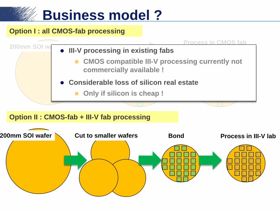
Business model ?
Need to cover full 200mm wafer (or 300mm ?)
Need to adapt processes to CMOS fab
Gold free contacts
III-V etching
…
Option I : all CMOS-fab processing
200mm SOI wafer Bond III-V diesProcess in CMOS fab
© intec 2009 - Photonics Research Group - http://photonics.intec.ugent.be
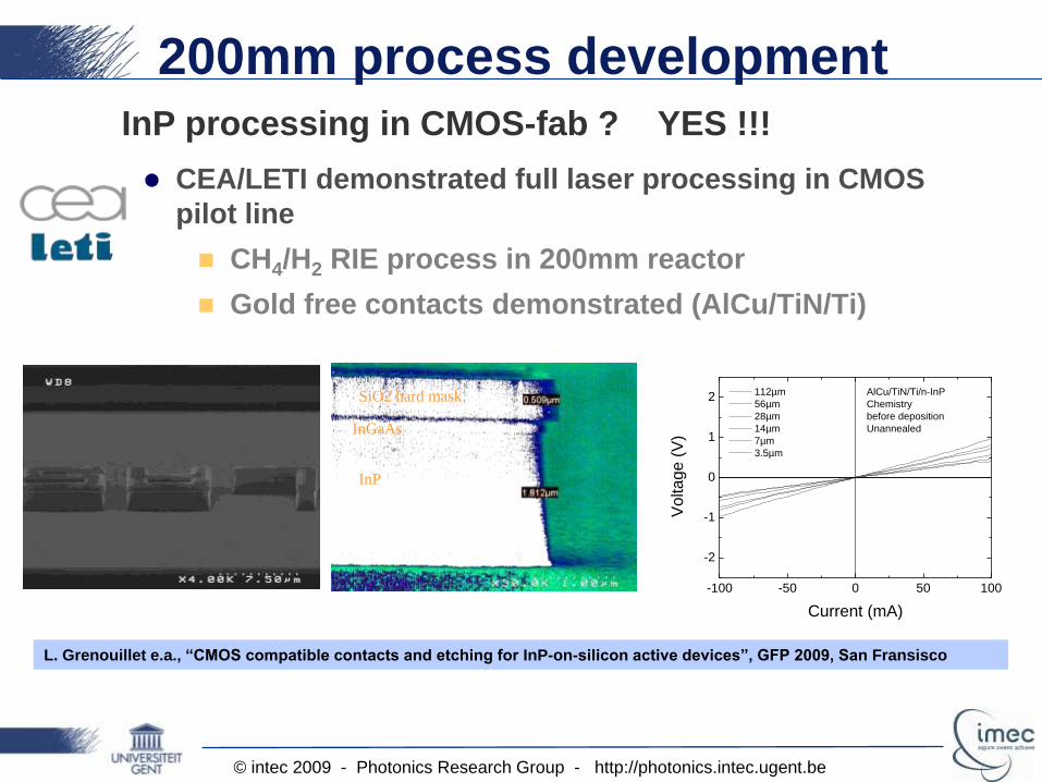
200mm process development
InP processing in CMOS-fab ? YES !!!
CEA/LETI demonstrated full laser processing in CMOS
pilot line
CH4/H2 RIE process in 200mm reactor
Gold free contacts demonstrated (AlCu/TiN/Ti)
L. Grenouillet e.a., “CMOS compatible contacts and etching for InP-on-silicon active devices”, GFP 2009, San Fransisco
SiO2 hard mask
InP
InGaAs
-100 -50 0 50 100
-2
-1
0
1
2 112µm
56µm
28µm
14µm
7µm
3.5µm
AlCu/TiN/Ti/n-InP
Chemistry
before deposition
Unannealed
Vo
lta
ge
(V
)
Current (mA)
Confidential93
2007
© CEA 2009. All rights reserved Any reproduction in whole or in part on any medium or use of the information contained herein
is prohibited without the prior written consent of CEA
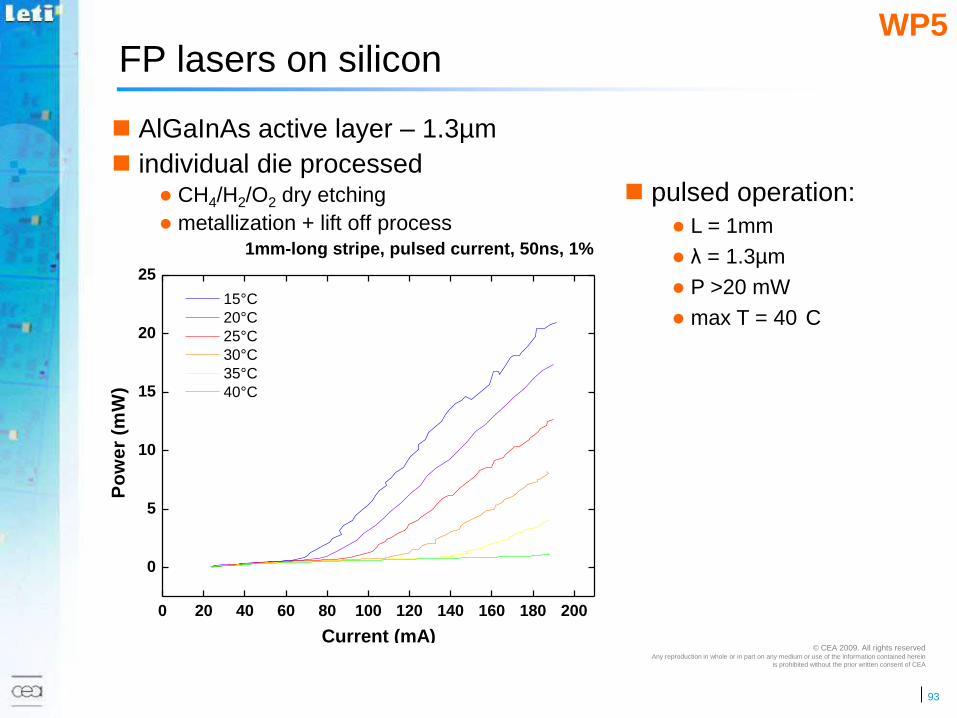
FP lasers on silicon
AlGaInAs active layer – 1.3µm
individual die processed CH4/H2/O2 dry etching
metallization + lift off process
pulsed operation:
L = 1mm
λ = 1.3µm
P >20 mW
max T = 40 C
0 20 40 60 80 100 120 140 160 180 200
0
5
10
15
20
25
15°C
20°C
25°C
30°C
35°C
40°C
Po
we
r (m
W)
Current (mA)
1mm-long stripe, pulsed current, 50ns, 1%
WP5
© intec 2009 - Photonics Research Group - http://photonics.intec.ugent.be
Business model ?Option I : all CMOS-fab processing
200mm SOI wafer Bond III-V diesProcess in CMOS fab
Option II : CMOS-fab + III-V fab processing
200mm SOI wafer Cut to smaller wafers Bond Process in III-V lab
III-V processing in existing fabs
CMOS compatible III-V processing currently not
commercially available !
Considerable loss of silicon real estate
Only if silicon is cheap !
© intec 2009 - Photonics Research Group - http://photonics.intec.ugent.be
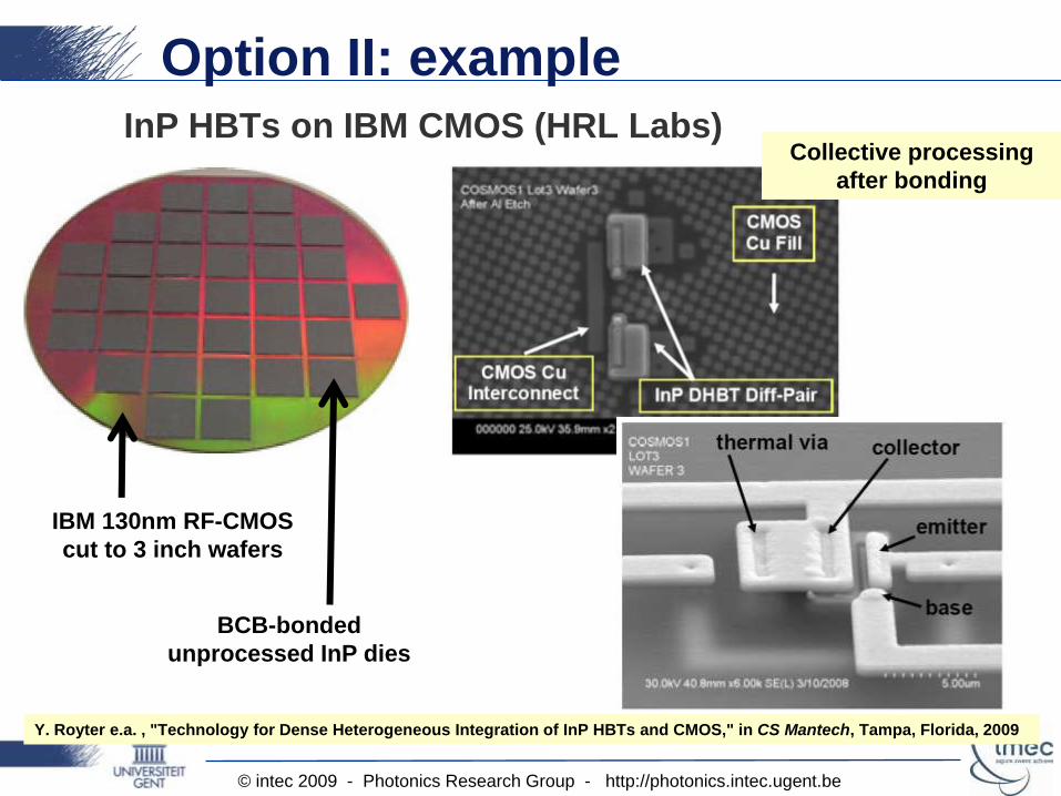
Option II: example
InP HBTs on IBM CMOS (HRL Labs)
Y. Royter e.a. , "Technology for Dense Heterogeneous Integration of InP HBTs and CMOS," in CS Mantech, Tampa, Florida, 2009
IBM 130nm RF-CMOS
cut to 3 inch wafers
BCB-bonded
unprocessed InP dies
Collective processing
after bonding
© intec 2009 - Photonics Research Group - http://photonics.intec.ugent.be
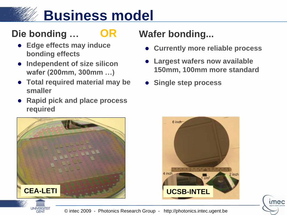
Business modelDie bonding … OR Edge effects may induce
bonding effects
Independent of size silicon
wafer (200mm, 300mm …)
Total required material may be
smaller
Rapid pick and place process
required
Wafer bonding...
Currently more reliable process
Largest wafers now available
150mm, 100mm more standard
Single step process
CEA-LETI UCSB-INTEL
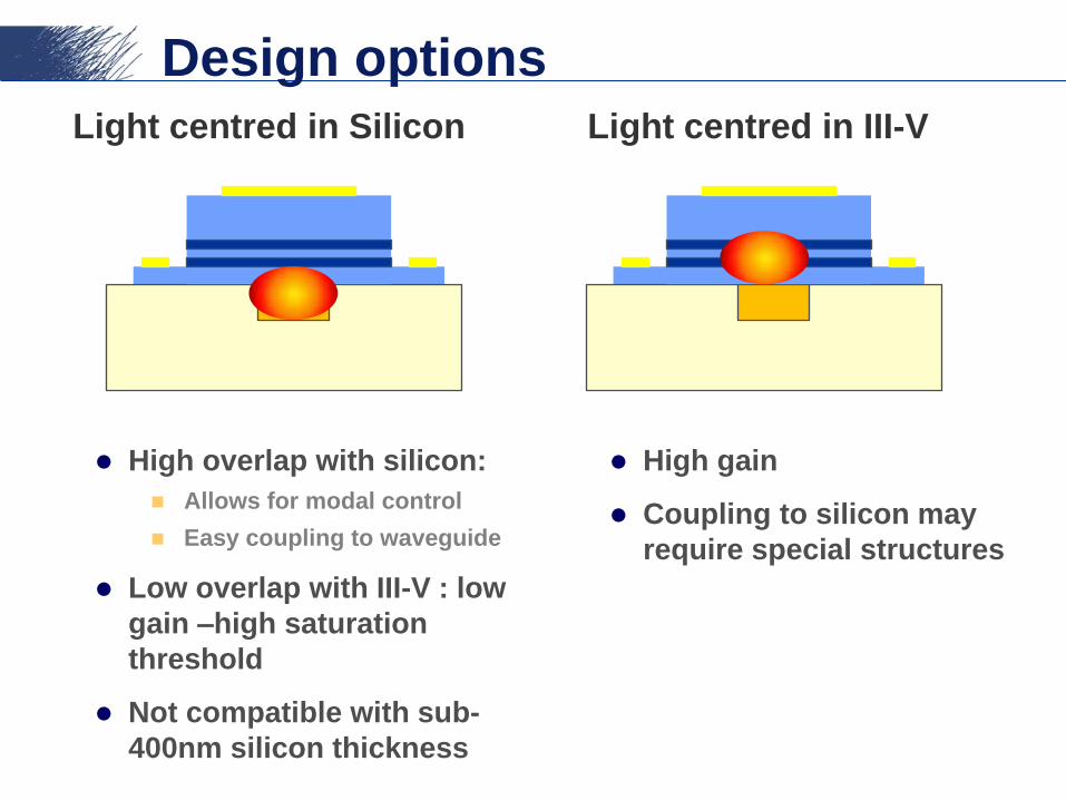
Design options
Light centred in Silicon
High overlap with silicon:
Allows for modal control
Easy coupling to waveguide
Low overlap with III-V : low
gain –high saturation
threshold
Not compatible with sub-
400nm silicon thickness
Light centred in III-V
High gain
Coupling to silicon may
require special structures
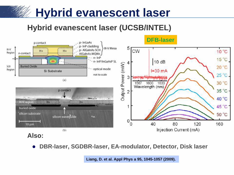
Hybrid evanescent laser
Hybrid evanescent laser (UCSB/INTEL)
Also:
DBR-laser, SGDBR-laser, EA-modulator, Detector, Disk laser
DFB-laser
Liang, D. et al. Appl Phys a 95, 1045-1057 (2009).

Microdisk laser
Microdisk laser
Whispering gallery mode
Evanescent coupling to silicon
150-350uA threshold
120uW output power (CW)Si substrate
SiO2Si waveguide
top contact
bottom contact active layer
tunnel junction
InP
2Rdisk
dox
wSi
t
ts
-0.5
0
0.5
1
1.5
2
2.5
0
5
10
15
20
25
30
35
40
45
0 1 2 3 4
Vo
lta
ge [
V]
Fib
er
co
up
led
ou
tpu
t p
ow
er
[uW
]
Current [mA]
-80
-70
-60
-50
-40
-30
-20
-10
1544 1564 1584 1604 1624
Sp
ec
tral p
ow
er
[dB
m]
Wavelength [nm]Spuesens e.a. ,GPF2009c
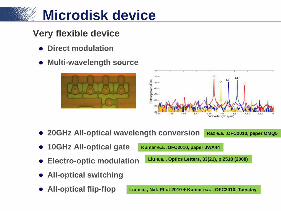
Microdisk device
Very flexible device
Direct modulation
Multi-wavelength source
20GHz All-optical wavelength conversion
10GHz All-optical gate
Electro-optic modulation
All-optical switching
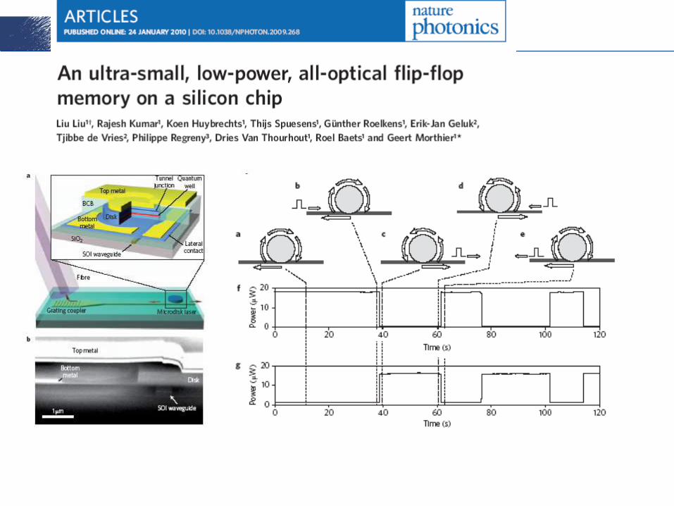
All-optical flip-flop
Raz e.a. ,OFC2010, paper OMQ5
Kumar e.a. ,OFC2010, paper JWA44
Liu e.a. , Nat. Phot 2010 + Kumar e.a. , OFC2010, Tuesday
Liu e.a. , Optics Letters, 33(21), p.2518 (2008)
102
2007
© CEA 2009. All rights reserved Any reproduction in whole or in part on any medium or use of the information contained herein
is prohibited without the prior written consent of CEA
Group Four Photonics Conference, FA1 September, 11th, 2009
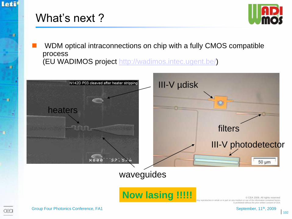
What’s next ?
WDM optical intraconnections on chip with a fully CMOS compatible process(EU WADIMOS project http://wadimos.intec.ugent.be/)
III-V µdisk
III-V photodetector
heaters
waveguides
filters
Now lasing !!!!!

http://photonics.intec.ugent.bePhotonics Research Group
Actives
sources
detectors
switchesmodulators
Outline
Passives
low loss
bend
coupling
complex filters
Integration
with electronicsall functions
applications
Monolithic vs. 3-D integration
Front-end: no thermal budget
Integrated in CMOS flow (on SOI only)
High process development cost
Compound yield
Little flexibility
Optical layer buried
Back-end: thermal budget < 400C
On top of CMOS(or in metal layers)
Serial process
Compound yield
Optical on topis possible
3-D: on top of CMOS
No thermal budget
Parallel process
No compound yield problem with die-to- wafer stacking (known good die)
Flexible choice of electronics and photonics
Other layers possible:MEMS, antennas
Optical layer on topis possible
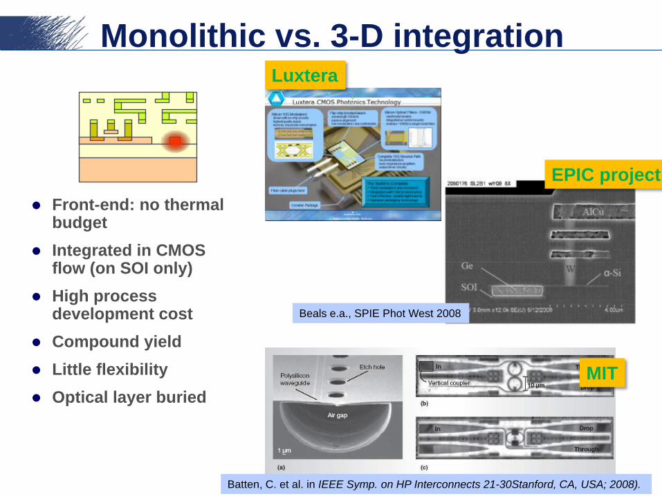
Monolithic vs. 3-D integration
Front-end: no thermal budget
Integrated in CMOS flow (on SOI only)
High process development cost
Compound yield
Little flexibility
Optical layer buried
Batten, C. et al. in IEEE Symp. on HP Interconnects 21-30Stanford, CA, USA; 2008).
Luxtera
MIT
EPIC project
Beals e.a., SPIE Phot West 2008
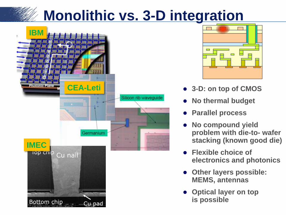
Monolithic vs. 3-D integration
3-D: on top of CMOS
No thermal budget
Parallel process
No compound yield problem with die-to- wafer stacking (known good die)
Flexible choice of electronics and photonics
Other layers possible:MEMS, antennas
Optical layer on topis possible
IBM
CEA-Leti
Cu nail
Cu pad
Top chip
Bottom chip
IMEC

http://photonics.intec.ugent.bePhotonics Research Group
Actives
sources
detectors
switchesmodulators
Passives
low loss
bend
coupling
complex filters
Integration
with electronicsall functions
applications
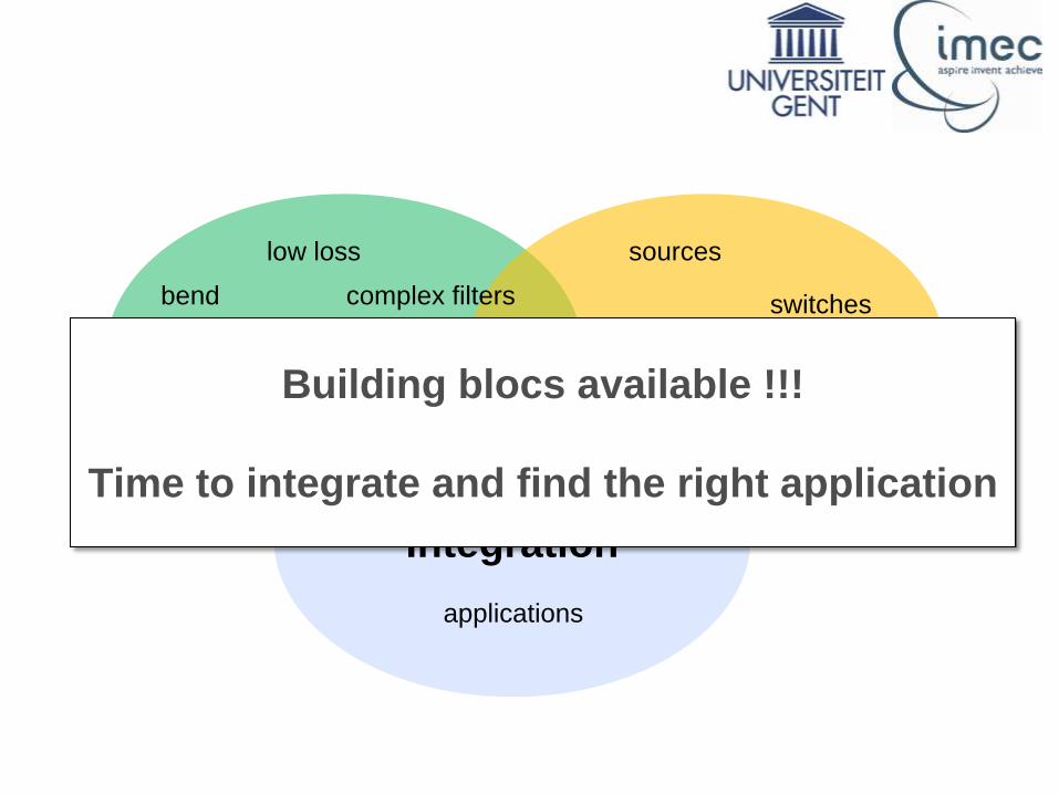
Building blocs available !!!
Time to integrate and find the right application
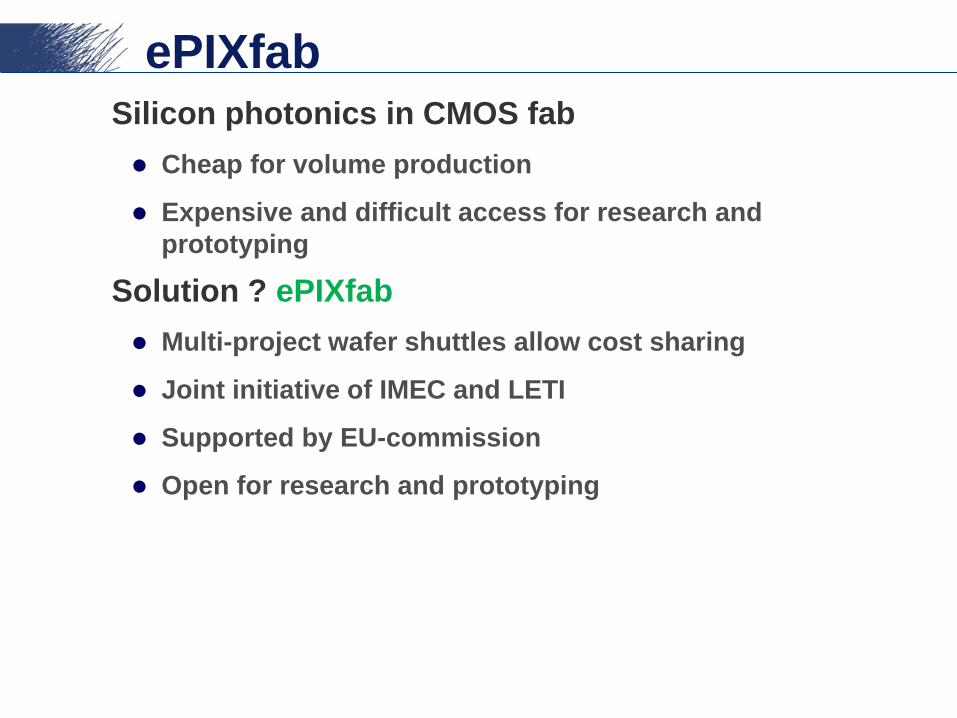
ePIXfab
Silicon photonics in CMOS fab
Cheap for volume production
Expensive and difficult access for research and
prototyping
Solution ? ePIXfab
Multi-project wafer shuttles allow cost sharing
Joint initiative of IMEC and LETI
Supported by EU-commission
Open for research and prototyping
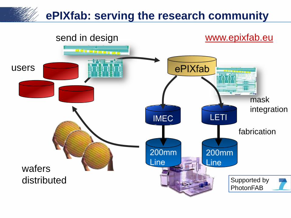
ePIXfab: serving the research community
users
mask
integration
send in design
fabrication
wafers
distributed
www.epixfab.eu
Supported by
PhotonFAB

ePIXfab: Practical information
Visit our web site:
www.epixfab.eu or www.siliconphotonics.eu
Information on calls
Technical docs
Coordinator:
Pieter Dumon
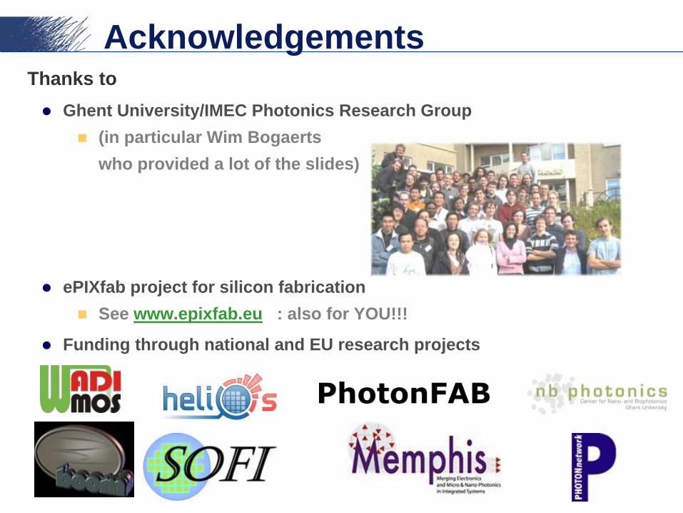
AcknowledgementsThanks to
Ghent University/IMEC Photonics Research Group
(in particular Wim Bogaerts
who provided a lot of the slides)
ePIXfab project for silicon fabrication
See www.epixfab.eu : also for YOU!!!
Funding through national and EU research projects