silicon photonics technology platform for integration of ... · luxtera proprietary silicon...
TRANSCRIPT
www.luxtera.com Luxtera Proprietary
Silicon Photonics Technology Platform for Integration of Optical IOs with ASICs
Peter De Dobbelaere
8/26/13
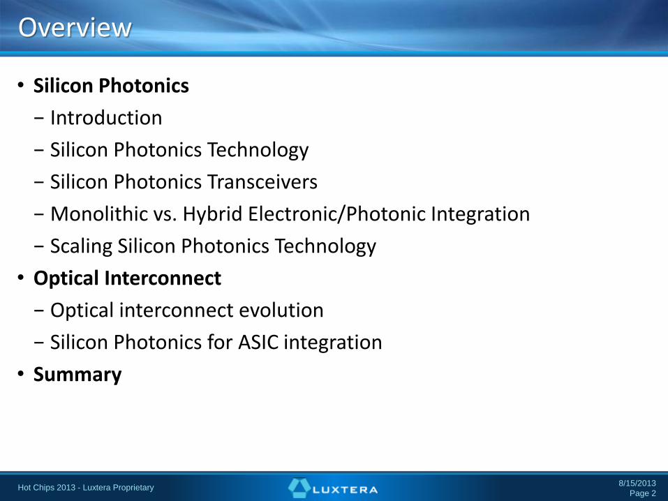
• Silicon Photonics
− Introduction
− Silicon Photonics Technology
− Silicon Photonics Transceivers
− Monolithic vs. Hybrid Electronic/Photonic Integration
− Scaling Silicon Photonics Technology
• Optical Interconnect
− Optical interconnect evolution
− Silicon Photonics for ASIC integration
• Summary
Overview
8/15/2013
Page 2 Hot Chips 2013 - Luxtera Proprietary
• Silicon Photonics Technology: − Silicon material system and silicon processing techniques to manufacture integrated optical devices − Silicon-on-insulator (SOI) substrates are used since they allow formation of optical waveguides − Besides passive photonic functions also capabilities for modulation and detecting of light are added.
Some groups also add monolithic integration of electronic circuits − Development started in earnest in early 2000s when sub 0.5 lithography became available
• Goal of Silicon Photonics: − Leverage as much as possible from the integrating electronic industry:
o Design infrastructure and methodologies o Wafer manufacturing and methodologies o Test infrastructure and methodologies o Assembly and packaging techniques
− Enable a very high level of integration: o Increased functionality and density o Simplification of optical and electrical packaging & test
• Applications for Silicon Photonics: − Most silicon photonics applications are in the area of high-speed communications − Also significant efforts emerge in the area of biochemical sensing and sensor applications in general
• Luxtera: − Produces Silicon Photonics based optical transceivers and chipsets since 2009, those are used in high
performance computing applications and advanced datacenters. − Developing chipsets and IP for high performance optical transceiver functions (Nx26 G and beyond)
Silicon Photonics Introduction
8/15/2013
Page 3 Hot Chips 2013 - Luxtera Proprietary
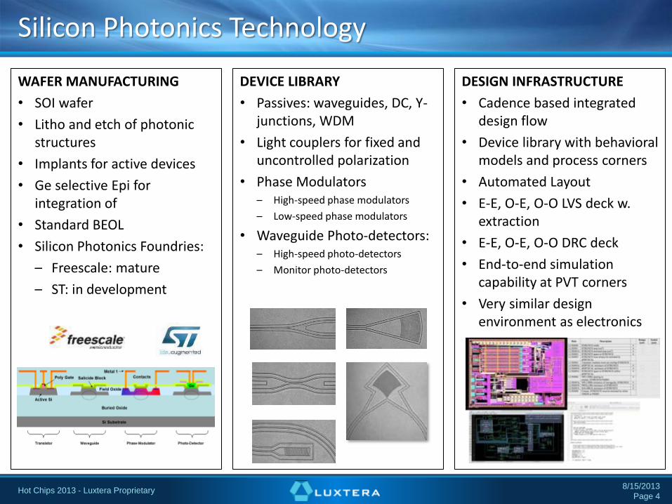
WAFER MANUFACTURING
• SOI wafer
• Litho and etch of photonic structures
• Implants for active devices
• Ge selective Epi for integration of
• Standard BEOL
• Silicon Photonics Foundries:
– Freescale: mature
– ST: in development
Silicon Photonics Technology
8/15/2013
Page 4 Hot Chips 2013 - Luxtera Proprietary
DEVICE LIBRARY
• Passives: waveguides, DC, Y-junctions, WDM
• Light couplers for fixed and uncontrolled polarization
• Phase Modulators – High-speed phase modulators
– Low-speed phase modulators
• Waveguide Photo-detectors: – High-speed photo-detectors
– Monitor photo-detectors
DESIGN INFRASTRUCTURE
• Cadence based integrated design flow
• Device library with behavioral models and process corners
• Automated Layout
• E-E, O-E, O-O LVS deck w. extraction
• E-E, O-E, O-O DRC deck
• End-to-end simulation capability at PVT corners
• Very similar design environment as electronics
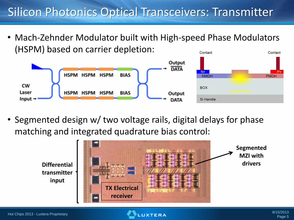
• Mach-Zehnder Modulator built with High-speed Phase Modulators (HSPM) based on carrier depletion:
• Segmented design w/ two voltage rails, digital delays for phase matching and integrated quadrature bias control:
Silicon Photonics Optical Transceivers: Transmitter
8/15/2013
Page 5 Hot Chips 2013 - Luxtera Proprietary
Segmented MZI with drivers Differential
transmitter input
TX Electrical receiver
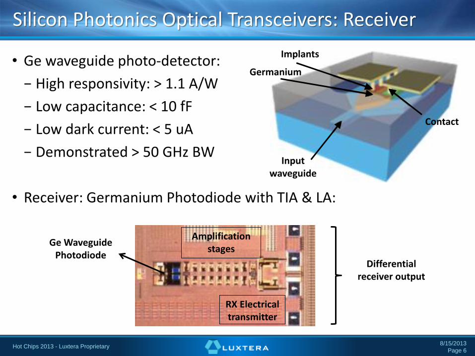
• Ge waveguide photo-detector:
− High responsivity: > 1.1 A/W
− Low capacitance: < 10 fF
− Low dark current: < 5 uA
− Demonstrated > 50 GHz BW
• Receiver: Germanium Photodiode with TIA & LA:
Silicon Photonics Optical Transceivers: Receiver
8/15/2013
Page 6 Hot Chips 2013 - Luxtera Proprietary
Amplification stages
Differential receiver output
RX Electrical transmitter
Ge Waveguide Photodiode
Input waveguide
Contact
Implants
Germanium
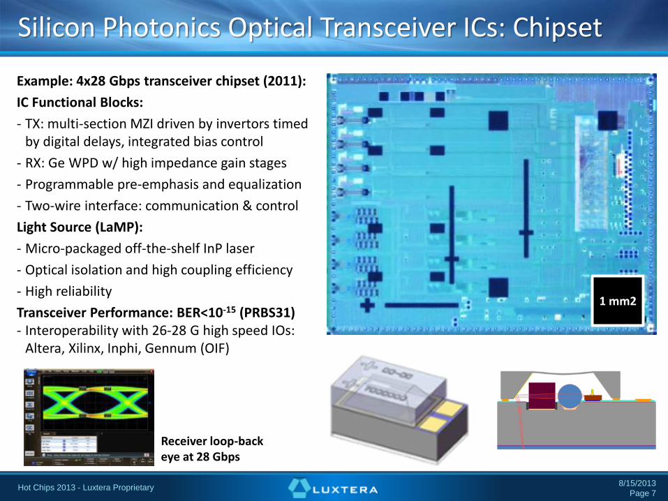
Example: 4x28 Gbps transceiver chipset (2011):
IC Functional Blocks:
- TX: multi-section MZI driven by invertors timed by digital delays, integrated bias control
- RX: Ge WPD w/ high impedance gain stages
- Programmable pre-emphasis and equalization
- Two-wire interface: communication & control
Light Source (LaMP):
- Micro-packaged off-the-shelf InP laser
- Optical isolation and high coupling efficiency
- High reliability
Transceiver Performance: BER<10-15 (PRBS31)
- Interoperability with 26-28 G high speed IOs: Altera, Xilinx, Inphi, Gennum (OIF)
Silicon Photonics Optical Transceiver ICs: Chipset
8/15/2013
Page 7 Hot Chips 2013 - Luxtera Proprietary
1 mm2
Receiver loop-back eye at 28 Gbps
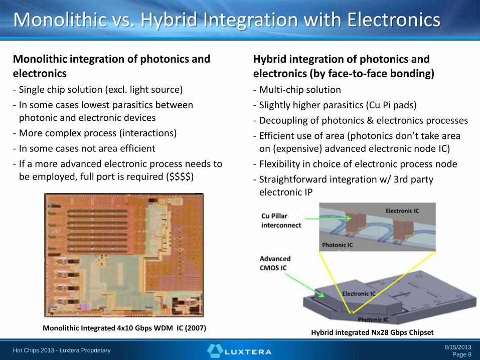
Monolithic integration of photonics and electronics
- Single chip solution (excl. light source)
- In some cases lowest parasitics between photonic and electronic devices
- More complex process (interactions)
- In some cases not area efficient
- If a more advanced electronic process needs to be employed, full port is required ($$$$)
Monolithic vs. Hybrid Integration with Electronics
Hybrid integration of photonics and electronics (by face-to-face bonding)
- Multi-chip solution
- Slightly higher parasitics (Cu Pi pads)
- Decoupling of photonics & electronics processes
- Efficient use of area (photonics don’t take area on (expensive) advanced electronic node IC)
- Flexibility in choice of electronic process node
- Straightforward integration w/ 3rd party electronic IP
8/15/2013
Page 8 Hot Chips 2013 - Luxtera Proprietary
Monolithic Integrated 4x10 Gbps WDM IC (2007) Hybrid integrated Nx28 Gbps Chipset
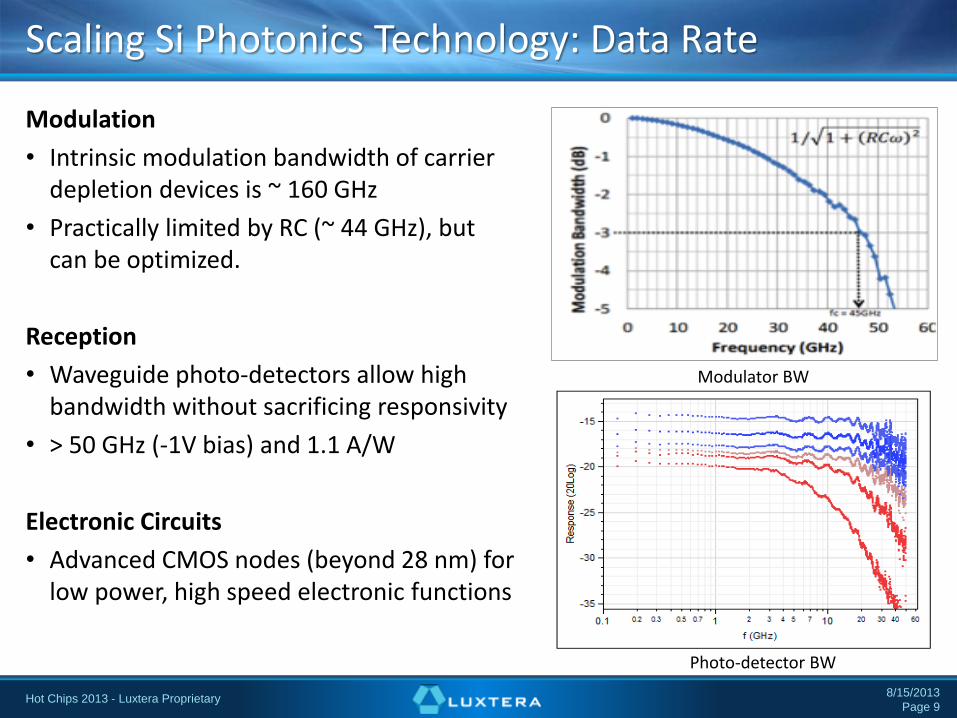
Modulation
• Intrinsic modulation bandwidth of carrier depletion devices is ~ 160 GHz
• Practically limited by RC (~ 44 GHz), but can be optimized.
Reception
• Waveguide photo-detectors allow high bandwidth without sacrificing responsivity
• > 50 GHz (-1V bias) and 1.1 A/W
Electronic Circuits
• Advanced CMOS nodes (beyond 28 nm) for low power, high speed electronic functions
Scaling Si Photonics Technology: Data Rate
8/15/2013
Page 9 Hot Chips 2013 - Luxtera Proprietary
Modulator BW
Photo-detector BW
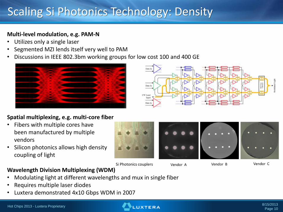
Multi-level modulation, e.g. PAM-N • Utilizes only a single laser • Segmented MZI lends itself very well to PAM • Discussions in IEEE 802.3bm working groups for low cost 100 and 400 GE Spatial multiplexing, e.g. multi-core fiber • Fibers with multiple cores have
been manufactured by multiple vendors
• Silicon photonics allows high density coupling of light
Wavelength Division Multiplexing (WDM) • Modulating light at different wavelengths and mux in single fiber • Requires multiple laser diodes • Luxtera demonstrated 4x10 Gbps WDM in 2007
Scaling Si Photonics Technology: Density
8/15/2013
Page 10 Hot Chips 2013 - Luxtera Proprietary
Si Photonics couplers
HIGHER DATA FLUX: • Data flux is limited:
– Shelf: face plate density limited by size of optical modules – ASIC: limited by electrical I/Os (~ 2500 bumps)
• Solutions: – Increase raw data rate – Integrate optical I/O with ASIC allowing higher density
LOWER POWER DISSIPATION: • Significant power is dissipated in electrical I/O drivers in ASIC
and optical transceivers: – Alleviated by shorter traces – Eliminated by close integration photonics & electronics
LONGER INTERCONNECT REACH: • New architectures for datacenters and HPC require longer
interconnect reaches at higher data rates while maintaining low latency
• Web 2.0 data centers and HPC represent large market for long reach optical interconnect solutions
• Long reach at high data rate can only be achieved by transmission over single mode fiber
High-Speed Interconnect Evolution
8/15/2013
Page 11 Hot Chips 2013 - Luxtera Proprietary
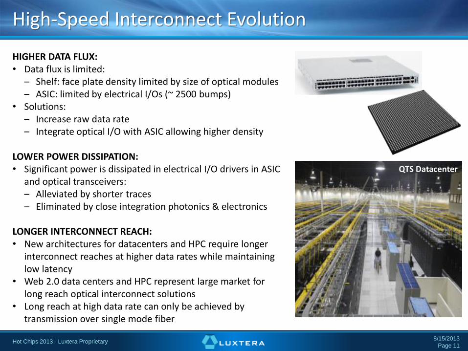
QTS Datacenter
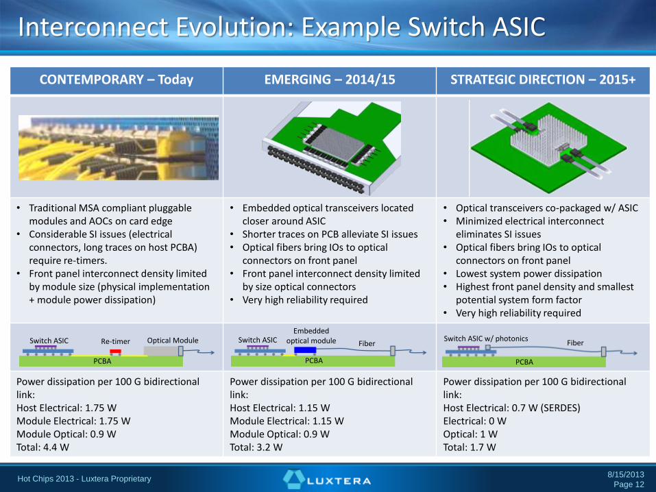
CONTEMPORARY – Today EMERGING – 2014/15 STRATEGIC DIRECTION – 2015+
• Traditional MSA compliant pluggable modules and AOCs on card edge
• Considerable SI issues (electrical connectors, long traces on host PCBA) require re-timers.
• Front panel interconnect density limited by module size (physical implementation + module power dissipation)
• Embedded optical transceivers located closer around ASIC
• Shorter traces on PCB alleviate SI issues • Optical fibers bring IOs to optical
connectors on front panel • Front panel interconnect density limited
by size optical connectors • Very high reliability required
• Optical transceivers co-packaged w/ ASIC • Minimized electrical interconnect
eliminates SI issues • Optical fibers bring IOs to optical
connectors on front panel • Lowest system power dissipation • Highest front panel density and smallest
potential system form factor • Very high reliability required
Power dissipation per 100 G bidirectional link: Host Electrical: 1.75 W Module Electrical: 1.75 W Module Optical: 0.9 W Total: 4.4 W
Power dissipation per 100 G bidirectional link: Host Electrical: 1.15 W Module Electrical: 1.15 W Module Optical: 0.9 W Total: 3.2 W
Power dissipation per 100 G bidirectional link: Host Electrical: 0.7 W (SERDES) Electrical: 0 W Optical: 1 W Total: 1.7 W
Interconnect Evolution: Example Switch ASIC
8/15/2013
Page 12 Hot Chips 2013 - Luxtera Proprietary
Embedded optical module Fiber Switch ASIC
PCBA
Fiber Switch ASIC w/ photonics
PCBA
Switch ASIC Re-timer Optical Module
PCBA
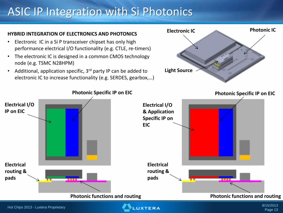
HYBRID INTEGRATION OF ELECTRONICS AND PHOTONICS
• Electronic IC in a Si P transceiver chipset has only high performance electrical I/O functionality (e.g. CTLE, re-timers)
• The electronic IC is designed in a common CMOS technology node (e.g. TSMC N28HPM)
• Additional, application specific, 3rd party IP can be added to electronic IC to increase functionality (e.g. SERDES, gearbox,…)
ASIC IP Integration with Si Photonics
8/15/2013
Page 13 Hot Chips 2013 - Luxtera Proprietary
Electronic IC Photonic IC
Light Source
Photonic Specific IP on EIC
Electrical I/O IP on EIC
Electrical I/O & Application Specific IP on EIC
Photonic Specific IP on EIC
Electrical routing & pads
Electrical routing & pads
Photonic functions and routing Photonic functions and routing
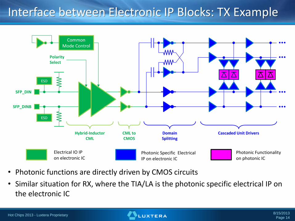
Interface between Electronic IP Blocks: TX Example
8/15/2013
Page 14 Hot Chips 2013 - Luxtera Proprietary
• Photonic functions are directly driven by CMOS circuits
• Similar situation for RX, where the TIA/LA is the photonic specific electrical IP on the electronic IC
ESD
ESD
SFP_DIN
SFP_DINB
Common Mode Control
Polarity Select
Hybrid-Inductor CML
Domain Splitting
CML to CMOS
Cascaded Unit Drivers
Electrical IO IP on electronic IC
Photonic Specific Electrical IP on electronic IC
Photonic Functionality on photonic IC
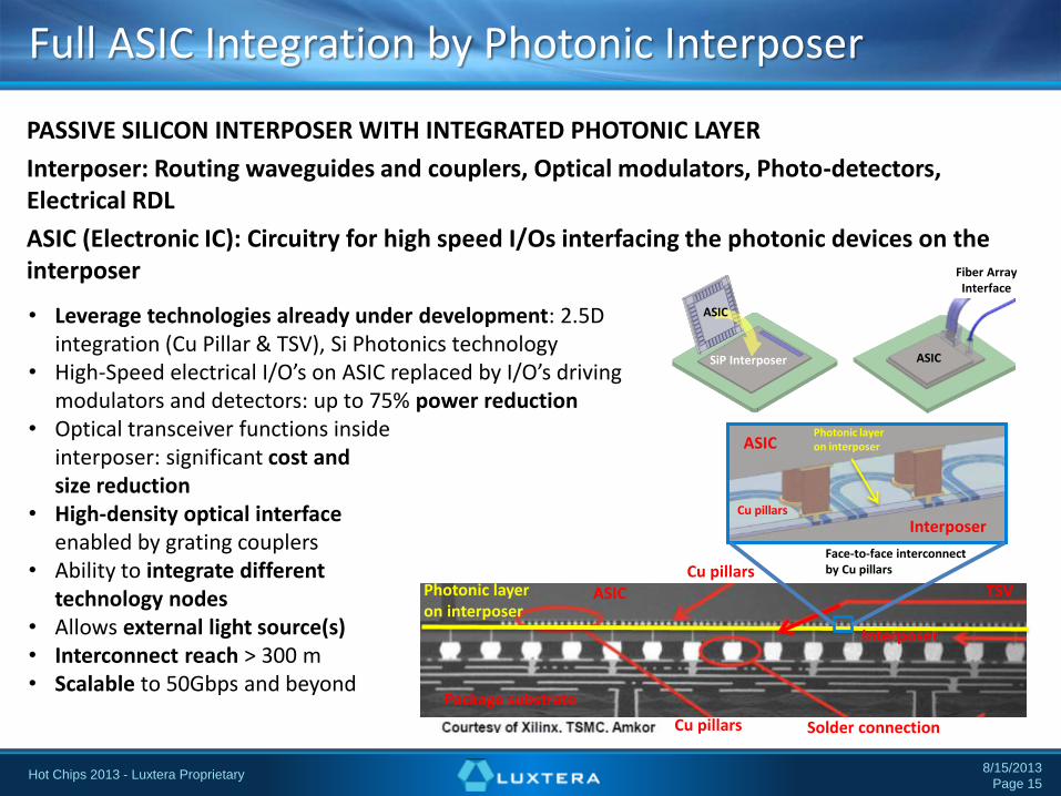
PASSIVE SILICON INTERPOSER WITH INTEGRATED PHOTONIC LAYER
Interposer: Routing waveguides and couplers, Optical modulators, Photo-detectors, Electrical RDL
ASIC (Electronic IC): Circuitry for high speed I/Os interfacing the photonic devices on the interposer
Full ASIC Integration by Photonic Interposer
8/15/2013
Page 15 Hot Chips 2013 - Luxtera Proprietary
• Leverage technologies already under development: 2.5D integration (Cu Pillar & TSV), Si Photonics technology
• High-Speed electrical I/O’s on ASIC replaced by I/O’s driving modulators and detectors: up to 75% power reduction
• Optical transceiver functions inside interposer: significant cost and size reduction
• High-density optical interface enabled by grating couplers
• Ability to integrate different technology nodes
• Allows external light source(s) • Interconnect reach > 300 m • Scalable to 50Gbps and beyond
SiP Interposer
ASIC
Face-to-face interconnect by Cu pillars
Photonic layer on interposer
Cu pillars Solder connection
Package substrate
Interposer
TSV
Cu pillars
Photonic layer on interposer
Interposer
ASIC
ASIC
Cu pillars
Fiber Array Interface
ASIC
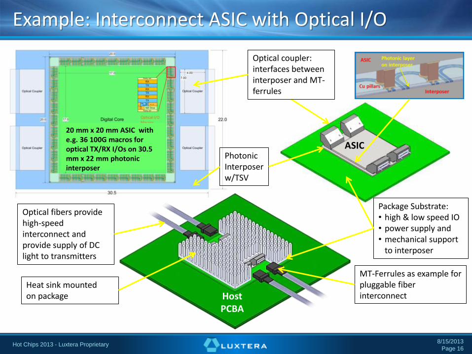
Example: Interconnect ASIC with Optical I/O
8/15/2013
Page 16 Hot Chips 2013 - Luxtera Proprietary
Host PCBA
Optical fibers provide high-speed interconnect and provide supply of DC light to transmitters
Heat sink mounted on package
Package Substrate: • high & low speed IO • power supply and • mechanical support
to interposer
MT-Ferrules as example for pluggable fiber interconnect
Optical coupler: interfaces between interposer and MT-ferrules
ASIC Photonic Interposer w/TSV
20 mm x 20 mm ASIC with e.g. 36 100G macros for optical TX/RX I/Os on 30.5 mm x 22 mm photonic interposer
• We highlighted Silicon Photonics Technology Platform and its scalability to increased data rates, higher interconnect densities and low system level power dissipation.
• Silicon photonics has been in production since 2009 and has shipped > 500K+ chipsets for use in High Performance Computing and Datacenters.
• We made the trade-off between hybrid and monolithic integration of photonics and electronics. Hybrid Silicon Photonics allows cost effective integration of photonics with advanced electronic nodes.
• By integrating 3rd Party IP in the electronic IC, hybrid integration enables a first level of ASIC integration with Photonics.
• A next level of ASIC integration is enabled by a “Silicon Photonics Interposer” where photonic capabilities are combined with hybrid integration with electronics and TSV technology.
Summary
8/15/2013
Page 17 Hot Chips 2013 - Luxtera Proprietary
This presentation shows the work of the entire Luxtera team, their contributions are greatly acknowledged.
Thank you for your interest.
Acknowledgements
8/15/2013
Page 18 Hot Chips 2013 - Luxtera Proprietary