silicon ring isolators with bonded nonreciprocal magneto ......bandwidth. the isolators using mo...
TRANSCRIPT
Silicon ring isolators with bonded nonreciprocal
magneto-optic garnets
Ming-Chun Tien,1,*
Tetsuya Mizumoto,2 Paolo Pintus,
1,3
Herbert Kromer,1 and John E. Bowers
1
1Department of Electrical and Computer Engineering, University of California, Santa Barbara, CA 93106, USA 2Department of Electrical and Electronic Engineering, Tokyo Institute of Technology, Tokyo, Japan
3Scuola Superiore Sant'Anna, 56124, Pisa, Italy
Abstract: A ring isolator is demonstrated for the first time by directly
bonding a cerium-substituted yttrium iron garnet (Ce:YIG) onto a silicon
ring resonator using oxygen plasma enhanced bonding. The silicon
waveguide is 600 nm wide and 295 nm thick with 500-nm-thick Ce:YIG on
the top to have reasonable nonreciprocal effect and low optical loss. With a
radial magnetic field applied to the ring isolator, it exhibits 9-dB isolation at
resonance in the 1550 nm wavelength regime.
©2011 Optical Society of America
OCIS codes: (230.3240) Isolators; (160.3820) Magneto-optical materials.
References and links
1. T. Shintaku, “Integrated optical isolator based on efficient nonreciprocal radiation mode conversion,” Appl.
Phys. Lett. 73(14), 1946–1948 (1998).
2. H. Shimizu and S. Goto, “Evanescent semiconductor active optical isolators for low insertion loss and high gain saturation power,” J. Lightwave Technol. 28(9), 1414–1419 (2010).
3. H. Shimizu and Y. Nakano, “Fabrication and characterization of an InGaAsP/InP active waveguide optical
isolator with 14.7 dB/mm TE mode nonreciprocal attenuation,” J. Lightwave Technol. 24(1), 38–43 (2006). 4. J. Fujita, M. Levy, R. M. Osgood, Jr., L. Wilkens, and H. Dotsch, “Waveguide optical isolator based on Mach-
Zehnder interferometer,” Appl. Phys. Lett. 76(16), 2158–2160 (2000).
5. H. Yokoi, T. Mizumoto, and Y. Shoji, “Optical nonreciprocal devices with a silicon guiding layer fabricated by
wafer bonding,” Appl. Opt. 42(33), 6605–6612 (2003).
6. H. Yokoi, T. Mizumoto, N. Shinjo, N. Futakuchi, and Y. Nakano, “Demonstration of an optical isolator with a
semiconductor guiding layer that was obtained by use of a nonreciprocal phase shift,” Appl. Opt. 39(33), 6158–6164 (2000).
7. Y. Shoji, T. Mizumoto, H. Yokoi, I. W. Hsieh, and R. M. Osgood, “Magneto-optical isolator with silicon
waveguides fabricated by direct bonding,” Appl. Phys. Lett. 92(7), 071117 (2008). 8. Z. Wang and S. Fan, “Optical circulators in two-dimensional magneto-optical photonic crystals,” Opt. Lett.
30(15), 1989–1991 (2005). 9. W. Śmigaj, J. Romero-Vivas, B. Gralak, L. Magdenko, B. Dagens, and M. Vanwolleghem, “Magneto-optical
circulator designed for operation in a uniform external magnetic field,” Opt. Lett. 35(4), 568–570 (2010).
10. A. Rostami, “Piecewise linear integrated optical device as an optical isolator using two-port nonlinear ring resonators,” Opt. Laser Technol. 39(5), 1059–1065 (2007).
11. L. Fan, J. Wang, H. Shen, L. T. Varghese, B. Niu, J. Ouyang, and M. Qi, “A CMOS compatible microring-based
on-chip isolator with 18dB optical isolation,” in Frontiers in Optics (OSA, 2010), paper FThQ4. 12. Z. Yu and S. Fan, “Complete optical isolation created by indirect interband photonic transitions,” Nat. Photonics
3(2), 91–94 (2009).
13. N. Kono, K. Kakihara, K. Saitoh, and M. Koshiba, “Nonreciprocal microresonators for the miniaturization of optical waveguide isolators,” Opt. Express 15(12), 7737–7751 (2007).
14. S. Yamamoto and T. Makimoto, “Circuit theory for a class of anisotropic and gyrotropic thin-film optical
waveguides and design of nonreciprocal devices for integrated optics,” J. Appl. Phys. 45(2), 882–888 (1974). 15. O. Zhuromskyy, H. Dotsch, M. Lohmeyer, L. Wilkens, and P. Hertel, “Magnetooptical waveguides with
polarization-independent nonreciprocal phase shift,” J. Lightwave Technol. 19(2), 214–221 (2001).
16. A. B. Fallahkhair, K. S. Li, and T. E. Murphy, “Vector finite difference modesolver for anisotropic dielectric waveguides,” J. Lightwave Technol. 26(11), 1423–1431 (2008).
17. P. Paolo, M.-C. Tien, and J. Bowers, “Design of magneto-optical ring isolator on SOI based on the finite element
method,” Photon. Technol. Lett. (submitted to). 18. A. Konrad, “High-order triangular finite elements for electromagnetic waves in anisotropic media,” IEEE Trans.
Microw. Theory Tech. 25(5), 353–360 (1977).
#144244 - $15.00 USD Received 18 Mar 2011; revised 18 Apr 2011; accepted 4 May 2011; published 1 Jun 2011(C) 2011 OSA 6 June 2011 / Vol. 19, No. 12 / OPTICS EXPRESS 11740
19. T. Shintaku, T. Uno, and M. Kobayashi, “Magneto-optic channel waveguides in Ce-substituted yttrium iron
garnet,” J. Appl. Phys. 74(8), 4877–4881 (1993). 20. D. Pasquariello and K. Hjort, “Plasma-assisted InP-to-Si low temperature wafer bonding,” IEEE J. Sel. Top.
Quantum Electron. 8(1), 118–131 (2002).
1. Introduction
The need for higher capacity and lower cost optical networks is driving the development of
photonic integrated circuits with various functions, such as lasing, modulation, switching,
splitting, and detection. Optical isolation is especially important to reduce unwanted optical
reflection back to semiconductor lasers, but is not yet a part of these integrated functions.
Conventional optical isolators, which consist of a Faraday rotator and a pair of polarizers, are
bulky and difficult to integrate. Several waveguide-type isolators have been explored for
integration of isolators.
Waveguide optical isolators use magneto-optic (MO) material, such as iron, cobalt, or
yttrium iron garnet (YIG), to generate a nonreciprocal effect with the existence of an external
magnetic field. The optical isolation can be achieved by nonreciprocal mode conversion [1],
nonreciprocal waveguide loss [2,3], and nonreciprocal phase shift [4,5]. The isolator utilizing
nonreciprocal mode conversion can convert backward light to a radiation mode and result in
higher optical loss, but phase matching between the modes is always an issue. Semiconductor
amplifiers (SOAs) combined with MO material with nonreciprocal loss can suppress the
backward light while providing gain to compensate the loss of the forward light. However, the
SOA requires continuous power consumption to compensate the extra insertion loss due to the
lossy MO material. Proper Mach-Zehnder Interferometer (MZI) design with nonreciprocal
phase shift generates constructive interference for forward light and destructive interference
for backward light to realize optical isolation. The MZI optical isolators have been
demonstrated on both III-V and silicon platforms [6,7].
Alternatively, resonant cavities, such as MO photonic crystals and ring resonators, can be
designed as optical isolators to reduce the footprint of devices at the expense of isolation
bandwidth. The isolators using MO photonic crystals require either precise magnetization
domain control over micron scale [8] or complex design of photonic crystals [9]. These issues
make them difficult to be experimentally realized. Using a nonlinear effect, optical isolation
was demonstrated based on ring resonators [10,11]. However, they have specific operation
power. In addition, optical isolation doesn’t happen with forward and backward light launched
simultaneously for these devices, and this is usually the case of required optical isolation for
semiconductor lasers. Another novel concept replying on temporal refractive-index
modulation is proposed to realize nonreciprocal frequency conversion using a non-magnetic
ring resonator [12]. The optical isolation can be achieved by incorporating an optical filter
with this nonreciprocal frequency converter.
2. Nonreciprocal ring resonator
The concept of nonreciprocal ring resonators was first proposed by Kono in 2007 [13].
However, the proposed structure is difficult to be realized in a practical approach. In this
paper we propose a simplified structure and demonstrate silicon optical ring isolators with
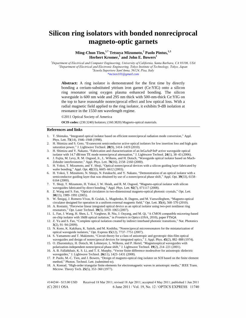
bonded MO garnets for the first time. The isolator consists of a ring resonator, a straight
coupled-waveguide, and a bonded MO garnet as shown in Fig. 1. In our experiment, cerium-
substituted yttrium iron garnet (Ce:YIG) is used as the MO material because of its high
Faraday coefficient and low optical loss in the 1550 nm regime. By applying a radial magnetic
field centered at the ring resonator, the nonreciprocal effect breaks the symmetry of the ring
resonator. As a result, the clockwise (CW)- and counterclockwise (CCW)- propagating modes
have different propagation constants and thus different resonance wavelengths. With a straight
waveguide coupled to the ring resonator, the forward light from the input is coupled to the
CW mode while the backward light is coupled to the CCW mode. If the transmission spectra
for the forward and backward directions are offset by half of the free spectral range, optical
#144244 - $15.00 USD Received 18 Mar 2011; revised 18 Apr 2011; accepted 4 May 2011; published 1 Jun 2011(C) 2011 OSA 6 June 2011 / Vol. 19, No. 12 / OPTICS EXPRESS 11741
isolation can be realized and optimized. With the optical input at off-resonance wavelength of
the CW mode and at on-resonance wavelength of the CCW mode, the forward light is
transmitted while the backward light is filtered out to realize optical isolation.
B
Ce:YIG
Top viewInput
(a) (b)
Fig. 1. Schematic of a ring isolator consisting of a ring resonator, a straight waveguide and a
bonded Ce:YIG layer as magneto-optic material. (a) top view (b) cross-section.
The propagation constant difference between CW and CCW modes with existence of an
external magnetic field is written as [14,15]
*
0* *
,
z
E Edxdy
E H E H dxdy
(1)
where E and H are the electrical and magnetic field, Δε is off-diagonal permittivity tensor of
MO material, and ε0 is the permittivity of MO material. The electrical and magnetic field
distributions are numerically solved by incorporating vectorial finite-difference algorithm into
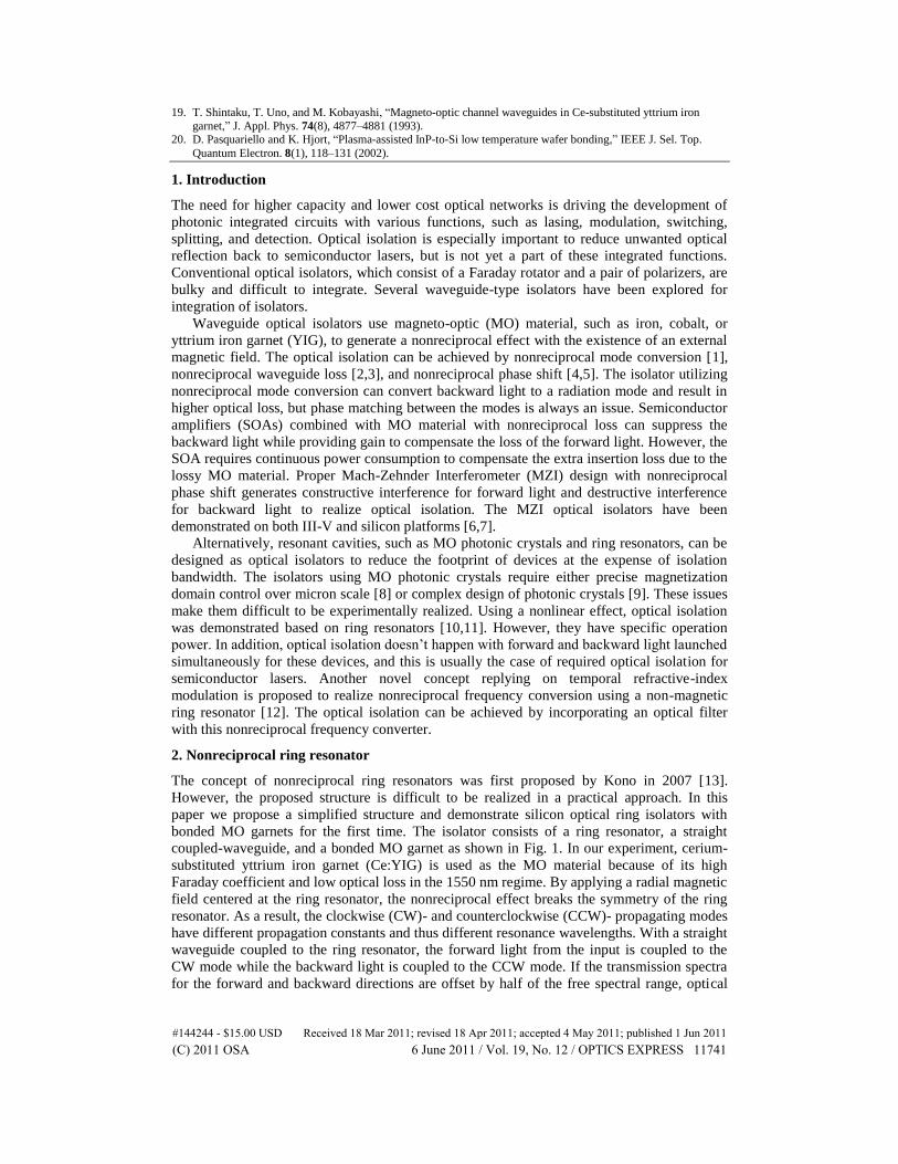
MATLAB [16]. Figure 2(a) shows the calculated Hx distribution profile of a 600-nm-wide and
300-nm-thick silicon waveguide with 500-nm-thick Ce:YIG as upper cladding and SiO2 as
lower cladding. Once the field distribution in the waveguide and Faraday coefficient of
Ce:YIG are known, the resonance wavelength split due to the propagation constant difference
between CW and CCW modes can be derived from Eq. (1). We also compare the analytic
solution with the simulation results using numerical full-vectorial finite element method
[17,18] as shown in Fig. 2(b). The results are slightly different probably because the mode
solver used for analytic solution doesn’t consider the small refractive index change due to the
nonreciprocal effect. Both methods indicate the maximum nonreciprocal effect as the silicon
waveguide thickness is approximately 220 nm. However, thinner waveguides result in higher
waveguide loss from the Ce:YIG layer, which has optical loss of 10-15 dB/cm. Therefore,
there is a trade-off between the nonreciprocal effect and the waveguide loss. The waveguide
thickness is chosen at 295 nm to have reasonable nonreciprocal effect and low optical loss in
our design.
#144244 - $15.00 USD Received 18 Mar 2011; revised 18 Apr 2011; accepted 4 May 2011; published 1 Jun 2011(C) 2011 OSA 6 June 2011 / Vol. 19, No. 12 / OPTICS EXPRESS 11742
x
y
Hx (mode 1)
02004006008000
200
400
600
800
1000
1200
1400
1600
1800
x
y
Hy (mode 1)
02004006008000
200
400
600
800
1000
1200
1400
1600
1800
x
y
Hx (mode 1)
0 200 400 600 8000
200
400
600
800
1000
1200
1400
1600
1800
x
y
Hy (mode 1)
0 200 400 600 8000
200
400
600
800
1000
1200
1400
1600
1800
BOX
Ce:YIG
SGGG
SiAir Air
(a) (b)
100 150 200 250 300 350 400
0.1
0.2
0.3
0.4
0.5
0.6
0.7
0.8 Finite element method
Perturbation method
Re
so
na
nc
e w
av
ele
ng
th s
pli
t (n
m)
Si waveguide thickness (nm)
Ce:YIG thickness : 500 nm
Fig. 2. (a) Calculated Hx field distribution in a 600 nm by 300 nm silicon waveguide with 500-
nm-thick Ce:YIG as upper cladding and silicon dioxide as lower cladding. (b) Resonance
wavelength split of the ring resonator as a function of waveguide thickness due to the nonreciprocal effect. The Faraday coefficient used for calculation is 4000 °/cm.
3. Fabrication and characterization of ring isolators
Silicon rectangular waveguides and ring resonators are fabricated on a silicon-on-insulator
(SOI) wafer with a 295-nm-thick silicon device layer and a 3-μm-thick buried oxide layer
using electron-beam lithography. The waveguide width is 600 nm, the ring radius is 900 μm,
and the gap between the ring and the waveguide is 250 nm. 500-nm-thick Ce:YIG is grown on
a (Ca, Mg, Zr)-substituted gadolinium gallium garnet (SGGG) substrate as MO material to
generate the nonreciprocal effect. The Ce:YIG has a Faraday-rotation coefficient as large as
4500 deg/cm at 1550 nm wavelength regime [19]. The Ce:YIG on an SGGG substrate is
then bonded to the fabricated silicon ring resonators using the following oxygen plasma
assisted low temperature bonding technique [7,20]. Both silicon and Ce:YIG are cleaned in
solvent followed by 20-minute ozone exposure. The cleaned silicon and Ce:YIG surfaces are
then activated by oxygen plasma. The activated surfaces are immediately soaked in NH4OH
vapor for two minutes to be terminated with OH groups. At this point, the samples are
attached to each other with assistance of a proper fixture to generate an external pressure of
3MPa. The whole fixture together with samples is annealed at 250°C for 1 hour to have a
strong bond. Higher annealing temperature causes sample cracking due to the mismatch of
thermal expansion coefficients between silicon and Ce:YIG.
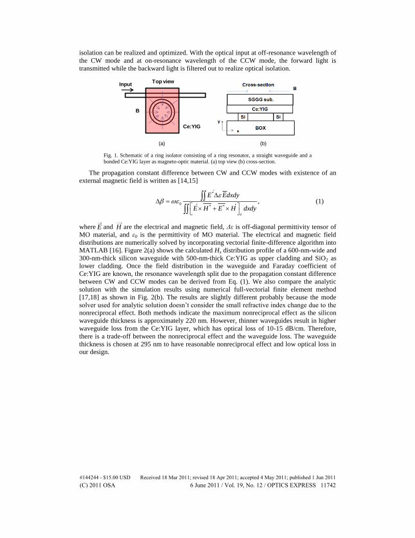
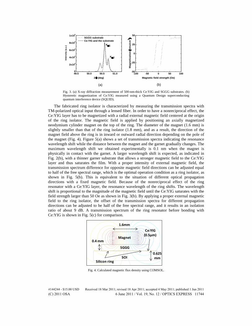
The crystallinity of the 500-nm-thick Ce:YIG film on an SGGG substrate was investigated
using Rigaku Smartlab High Resolution X-ray Diffractometer. The measured diffraction curve
of the thin film is shown in the solid line of Fig. 3(a) while the dashed line shows the
diffraction curve of the substrate only. Because the crystal orientation of the SGGG substrate
is in (111) direction, Ce:YIG also grows in the (111) direction. Ce:YIG has a cubic crystal
structure with a lattice constant of 1.253 nm, whose corresponding X-ray diffraction peak is
approximately at 50.4 degree as shown in Fig. 3(a). The X-ray diffraction also exhibits the
crystal structure of the SGGG substrate, which has lattice constant of 1.249 nm. It should be
noted that all the peaks are composed by Kα1 and Kα2 peaks due to multi-wavelengths of the
X-ray source.
The magnetization of Ce:YIG was also investigated using a Quantum Design
superconducting quantum interference device (SQUID) magnetometer. The magnetization
versus magnetic field strength was measured at room temperature with a sample size of 5 mm
by 5 mm. The measured curve consists of the ferromagnetic Ce:YIG layer and the
paramagnetic SGGG substrate. Figure 3(b) shows the curves after subtracting the contribution
from the substrate. The saturation magnetization is estimated to be ~40 emu/cm3 with external
magnetic field strength larger than 50 Oe. This implies that the required external magnetic
flux density to saturate the film is ~50 Gauss.
#144244 - $15.00 USD Received 18 Mar 2011; revised 18 Apr 2011; accepted 4 May 2011; published 1 Jun 2011(C) 2011 OSA 6 June 2011 / Vol. 19, No. 12 / OPTICS EXPRESS 11743
-100 -50 0 50 100-50
-25
0
25
50
Ma
gn
eti
za
tio
n (
em
u/c
m3)
Magnetic field strength (Oe)
49.5 50.0 50.5 51.00
2x10⁵
4x10⁵
6x10⁵
8x10⁵
1x10⁶
K2
K1
Inte
ns
ity
(a
.u.)
2 (deg)
SGGG substrate
Ce:YIG and the substrate
(a) (b)
Fig. 3. (a) X-ray diffraction measurement of 500-nm-thick Ce:YIG and SGGG substrates. (b) Hysteretic magnetization of Ce:YIG measured using a Quantum Design superconducting
quantum interference device (SQUID).
The fabricated ring isolator is characterized by measuring the transmission spectra with
TM-polarized optical input through a lensed fiber. In order to have a nonreciprocal effect, the
Ce:YIG layer has to be magnetized with a radial external magnetic field centered at the origin
of the ring isolator. The magnetic field is applied by positioning an axially magnetized
neodymium cylinder magnet on the top of the ring. The diameter of the magnet (1.6 mm) is
slightly smaller than that of the ring isolator (1.8 mm), and as a result, the direction of the
magnet field above the ring is in inward or outward radial direction depending on the pole of
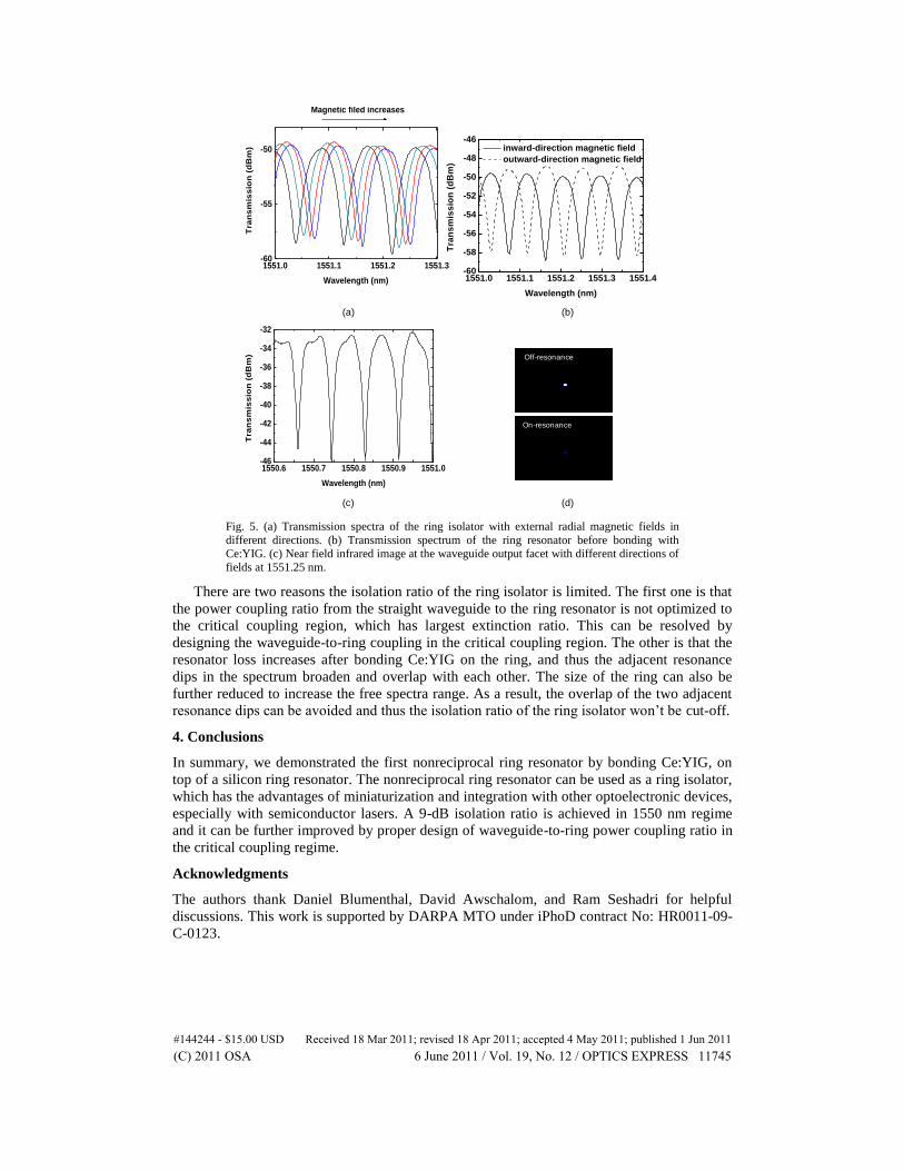
the magnet (Fig. 4). Figure 5(a) shows a set of transmission spectra indicating the resonance
wavelength shift while the distance between the magnet and the garnet gradually changes. The
maximum wavelength shift we obtained experimentally is 0.1 nm when the magnet is
physically in contact with the garnet. A larger wavelength shift is expected, as indicated in
Fig. 2(b), with a thinner garner substrate that allows a stronger magnetic field to the Ce:YIG
layer and thus saturates the film. With a proper intensity of external magnetic field, the
transmission spectrum difference for opposite magnetic field directions can be adjusted equal
to half of the free spectral range, which is the optimal operation condition as a ring isolator, as
shown in Fig. 5(b). This is equivalent to the situation of different optical propagation
directions with a fixed magnetic field. Because of the nonreciprocal effect of the ring
resonator with a Ce:YIG layer, the resonance wavelength of the ring shifts. The wavelength
shift is proportional to the magnitude of the magnetic field until the Ce:YIG saturates with the
field strength larger than 50 Oe as shown in Fig. 3(b). By applying a proper external magnetic
field to the ring isolator, the offset of the transmission spectra for different propagation
directions can be adjusted to be half of the free spectral range, and it results in an isolation
ratio of about 9 dB. A transmission spectrum of the ring resonator before bonding with
Ce:YIG is shown in Fig. 5(c) for comparison.
Magnet
SGGG
Ce:YIG(0.5μm)
1.6mm
0.4 mm
SOISilicon ring
0.625 mm
Fig. 4. Calculated magnetic flux density using COMSOL.
#144244 - $15.00 USD Received 18 Mar 2011; revised 18 Apr 2011; accepted 4 May 2011; published 1 Jun 2011(C) 2011 OSA 6 June 2011 / Vol. 19, No. 12 / OPTICS EXPRESS 11744
1551.0 1551.1 1551.2 1551.3 1551.4-60
-58
-56
-54
-52
-50
-48
-46
Tra
ns
mis
sio
n (
dB
m)
Wavelength (nm)
inward-direction magnetic field
outward-direction magnetic field
1550.6 1550.7 1550.8 1550.9 1551.0-46
-44
-42
-40
-38
-36
-34
-32
Tra
ns
mis
sio
n (
dB
m)
Wavelength (nm)
(c)
On-resonance
Off-resonance
(d)
1551.0 1551.1 1551.2 1551.3-60
-55
-50
Tra
ns
mis
sio
n (
dB
m)
Wavelength (nm)
Magnetic filed increases
(a) (b)
Fig. 5. (a) Transmission spectra of the ring isolator with external radial magnetic fields in
different directions. (b) Transmission spectrum of the ring resonator before bonding with Ce:YIG. (c) Near field infrared image at the waveguide output facet with different directions of
fields at 1551.25 nm.
There are two reasons the isolation ratio of the ring isolator is limited. The first one is that
the power coupling ratio from the straight waveguide to the ring resonator is not optimized to
the critical coupling region, which has largest extinction ratio. This can be resolved by
designing the waveguide-to-ring coupling in the critical coupling region. The other is that the
resonator loss increases after bonding Ce:YIG on the ring, and thus the adjacent resonance
dips in the spectrum broaden and overlap with each other. The size of the ring can also be
further reduced to increase the free spectra range. As a result, the overlap of the two adjacent
resonance dips can be avoided and thus the isolation ratio of the ring isolator won’t be cut-off.
4. Conclusions
In summary, we demonstrated the first nonreciprocal ring resonator by bonding Ce:YIG, on
top of a silicon ring resonator. The nonreciprocal ring resonator can be used as a ring isolator,
which has the advantages of miniaturization and integration with other optoelectronic devices,
especially with semiconductor lasers. A 9-dB isolation ratio is achieved in 1550 nm regime
and it can be further improved by proper design of waveguide-to-ring power coupling ratio in
the critical coupling regime.
Acknowledgments
The authors thank Daniel Blumenthal, David Awschalom, and Ram Seshadri for helpful
discussions. This work is supported by DARPA MTO under iPhoD contract No: HR0011-09-
C-0123.
#144244 - $15.00 USD Received 18 Mar 2011; revised 18 Apr 2011; accepted 4 May 2011; published 1 Jun 2011(C) 2011 OSA 6 June 2011 / Vol. 19, No. 12 / OPTICS EXPRESS 11745