silver nanowires as surface plasmon · pdf filesilver nanowires as surface plasmon resonators...
TRANSCRIPT

PRL 95, 257403 (2005) P H Y S I C A L R E V I E W L E T T E R S week ending16 DECEMBER 2005
Silver Nanowires as Surface Plasmon Resonators
Harald Ditlbacher,1 Andreas Hohenau,1 Dieter Wagner,2 Uwe Kreibig,2 Michael Rogers,3 Ferdinand Hofer,3
Franz R. Aussenegg,1 and Joachim R. Krenn1
1Institute of Physics, Karl-Franzens-University, 8010 Graz, Austria2Physikalisches Institut I.A, RWTH, 52074 Aachen, Germany
3Austrian Centre for Electron Microscopy and Nanoanalysis, 8010 Graz, Austria(Received 6 September 2005; published 16 December 2005)
0031-9007=
We report on chemically prepared silver nanowires (diameters around 100 nm) sustaining surfaceplasmon modes with wavelengths shortened to about half the value of the exciting light. As we find byscattered light spectroscopy and near-field optical microscopy, the nonradiating character of these modestogether with minimized damping due to the well developed wire crystal structure gives rise to largevalues of surface plasmon propagation length and nanowire end face reflectivity of about 10 �m and 25%,respectively. We demonstrate that these properties allow us to apply the nanowires as efficient surfaceplasmon Fabry-Perot resonators.
DOI: 10.1103/PhysRevLett.95.257403 PACS numbers: 78.67.Lt, 73.20.Mf, 73.22.Lp, 78.66.�w
FIG. 1 (color online). Scanning electron micrographs of a18:6 �m long silver nanowire. The wire diameter of 120 nmwas independently determined by measuring the height of thenanowire by atomic force microscopy. In the image, the wirediameter is larger, as the sample was sputtered with 30 nm goldto provide electric conductivity for electron microscopy imag-ing.
The integration of optics with nanotechnology is hin-dered by the lack of subwavelength photonic elements.Surface plasmons—coupled excitations of light and elec-trons at a metal surface—are a potential solution to thisproblem, as they allow the concentration of light to sub-wavelength volumes [1]. Recent advances in plasmonicshave demonstrated surface plasmon waveguiding and op-tical addressing and, thus, the feasibility of integratedplasmon optics. Waveguiding in �m-wide metal thin films[2–4] and nanowires [5–9] and passive [10] and dynamiccontrol [11] thereof has been shown. Here we report theexperimental realization of Fabry-Perot–type plasmon res-onators by chemically prepared silver wires with�100 nmcross-section diameters and lengths up to about 20 �m.Our resonators rely on specific plasmon modes with wave-lengths considerably shorter than the exciting light wave-length. These modes are not radiation damped and lead,thus, to unexpectedly large propagation lengths. Besideslaying the foundation for wavelength selective devices,nanowire resonators might, therefore, enable improvedspatial resolution in plasmon-based photonic circuitry.
Provided that the wire end faces reflect an incidentsurface plasmon, a nanowire can be turned into a surfaceplasmon resonator. Then resonator modes, i.e., standingsurface plasmon waves along the nanowire axis, existwhenever an integer of half the surface plasmon wave-length equals the wire length. The maximum achievableresonator length is, however, limited by the metallic damp-ing of the surface plasmon mode [12]. We investigatechemically prepared silver nanowires with a well definedcrystal and surface structure, thereby minimizing surfaceplasmon damping due to scattering at roughness, domainboundaries, or defects. The nanowires are produced by achemical reduction method of silver ions in an aqueouselectrolyte solution. The fabrication process yields nano-wires with cross-section diameters of 13–130 nm andlengths up to 70 �m [13]. High resolution transmission
05=95(25)=257403(4)$23.00 25740
electron microscopy reveals the nanowires to consist of alattice aligned bundle of five monocrystalline rods of atriangular cross section forming an almost regular pentago-nal cross section [13]. Casting the purified electrolyte on aglass slide and letting it dry under ambient conditionsyields well separated individual wires on the slide. Onesuch wire is shown in Fig. 1.
Surface plasmon propagation along a nanowire can bestraightforwardly demonstrated by local optical excitation[7]. We focus a laser beam under normal incidence withrespect to the substrate plane with a microscope objective(60�, numerical aperture of 1.4) onto one end face (inputend) of a 18:6 �m long nanowire with a diameter of120 nm; see Fig. 2(a). The laser wavelength is 785 nm,and the polarization is oriented along the nanowire axis.
3-1 © 2005 The American Physical Society
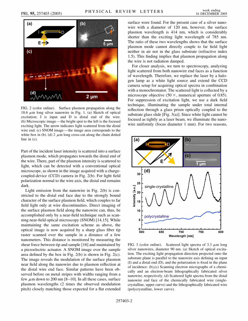
FIG. 3 (color online). Scattered light spectra of 3:3 �m longsilver nanowires, diameter 90 nm. (a) Sketch of optical excita-tion. The exciting light propagation direction projected onto thesubstrate plane is parallel to the nanowire axis defining an input(I) and a distal end (D), and the polarization is fixed in the planeof incidence. (b),(c) Scanning electron micrographs of a chemi-cally and an electron-beam lithographically fabricated silvernanowire, respectively. (d) Scattered light spectra from the distalnanowire end face of the chemically fabricated wire (single-crystalline, upper curve) and the lithographically fabricated wire(polycrystalline, lower curve).
FIG. 2 (color online). Surface plasmon propagation along the18:6 �m long silver nanowire in Fig. 1. (a) Sketch of opticalexcitation; I is input and D is distal end of the wire.(b) Microscopic image—the bright spot to the left is the focusedexciting light. The arrow indicates light scattered from the distalwire end. (c) SNOM image—the image area corresponds to thewhite box in (b). (d) 2 �m long cross-cut along the chain dottedline in (c).
PRL 95, 257403 (2005) P H Y S I C A L R E V I E W L E T T E R S week ending16 DECEMBER 2005
Part of the incident laser intensity is scattered into a surfaceplasmon mode, which propagates towards the distal end ofthe wire. There, part of the plasmon intensity is scattered tolight, which can be detected with a conventional opticalmicroscope, as shown in the image acquired with a charge-coupled-device (CCD) camera in Fig. 2(b). For light fieldpolarization normal to the wire axis, the distal end remainsdark.
Light emission from the nanowire in Fig. 2(b) is con-stricted to the distal end face due to the strongly boundcharacter of the surface plasmon field, which couples to farfield light only at wire discontinuities. Direct imaging ofthe surface plasmon field along the nanowire can, thus, beaccomplished only by a near-field technique such as scan-ning near-field optical microscopy (SNOM) [14,15]. Whilemaintaining the same excitation scheme as above, theoptical image is now acquired by a sharp glass fiber tipraster scanned over the sample in a distance of a fewnanometers. This distance is monitored by measuring theshear force between tip and sample [16] and maintained bya piezoelectric actuator. A SNOM image over the samplearea defined by the box in Fig. 2(b) is shown in Fig. 2(c).The image reveals the modulation of the surface plasmonnear field along the nanowire due to plasmon reflection atthe distal wire end face. Similar patterns have been ob-served before on metal stripes with widths ranging from afew�m down to 200 nm [8–10]. In all these cases, surfaceplasmon wavelengths (2 times the observed modulationpitch) closely matching those expected for a flat extended
25740
surface were found. For the present case of a silver nano-wire with a diameter of 120 nm, however, the surfaceplasmon wavelength is 414 nm, which is considerablyshorter than the exciting light wavelength of 785 nm.The ratio of these two wavelengths shows that the surfaceplasmon mode cannot directly couple to far field lightneither in air nor in the glass substrate (refractive index1.5). This finding implies that plasmon propagation alongthe wire is not radiation damped.
For closer analysis, we turn to spectroscopy, analyzinglight scattered from both nanowire end faces as a functionof wavelength. Therefore, we replace the laser by a halo-gen lamp as a white light source and extend the CCDcamera setup for acquiring optical spectra in combinationwith a monochromator. The scattered light is collected by amicroscope objective (50�, numerical aperture of 0.85).For suppression of excitation light, we use a dark fieldtechnique, illuminating the sample under total internalreflection through a glass prism optically coupled to thesubstrate glass slide [Fig. 3(a)]. Since white light cannot befocused as tightly as a laser beam, we illuminate the nano-wire uniformly (focus diameter 1 mm). For two reasons,
3-2
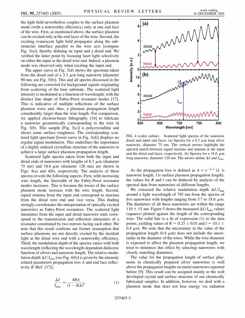
FIG. 4 (color online). Scattered light spectra of the nanowiredistal and input end faces. (a) Spectra for a 8:3 �m long silvernanowire, diameter 75 nm. The vertical arrows highlight thespectral match between signal maxima and minima at the inputand the distal end faces, respectively. (b) Spectra for a 18:6 �mlong nanowire, diameter 120 nm. The arrows define �I and Imin.
PRL 95, 257403 (2005) P H Y S I C A L R E V I E W L E T T E R S week ending16 DECEMBER 2005
the light field nevertheless couples to the surface plasmonmode (with a noteworthy efficiency) only at one end faceof the wire. First, as mentioned above, the surface plasmoncan be excited only at the end faces of the wire. Second, theexciting evanescent light field propagates along the sub-strate/air interface parallel to the wire axis [compareFig. 3(a)], thereby defining an input and a distal end. Weverified the latter point by focusing laser light selectivelyon either the input or the distal wire end. Indeed, a plasmonmode was observed only when exciting the input end.
The upper curve in Fig. 3(d) shows the spectrum takenfrom the distal end of a 3:3 �m long nanowire [diameter90 nm, see Fig. 3(b)]. This and all spectra discussed in thefollowing are corrected for background signals originatingfrom scattering of the bare substrate. The scattered lightintensity is modulated as a function of wavelength, with thedistinct line shape of Fabry-Perot resonator modes [17].This is indicative of multiple reflections of the surfaceplasmon wave and, thus, a plasmon propagation lengthconsiderably larger than the wire length. For comparison,we applied electron-beam lithography [18] to fabricatea nanowire geometrically corresponding to the wire inFig. 3(b). This sample [Fig. 3(c)] is polycrystalline andshows some surface roughness. The corresponding scat-tered light spectrum [lower curve in Fig. 3(d)] displays noregular signal modulation. This underlines the importanceof a highly ordered crystalline structure of the nanowire toachieve a large surface plasmon propagation length.
Scattered light spectra taken from both the input anddistal ends of nanowires with lengths of 8:3 �m (diameter75 nm) and 18:6 �m (diameter 120 nm) are shown inFigs. 4(a) and 4(b), respectively. The analysis of thesespectra reveals the following aspects. First, with increasingwire length, the linewidth of the Fabry-Perot resonatormodes increases. This is because the losses of the surfaceplasmon mode increase with the wire length. Second,signal minima from the input end correspond to maximafrom the distal wire end and vice versa. This findingstrongly corroborates the interpretation of optically excitednanowires as Fabry-Perot resonators. The scattered lightintensities from the input and distal nanowire ends corre-spond to the transmission and reflection intensities of aresonator constituted by two mirrors facing each other. Wenote that this result confirms our former assumption thatsurface plasmons are not directly excited by the incidentlight at the distal wire end with a noteworthy efficiency.Third, the modulation depth of the spectra varies with bothwavelength (reflecting the wavelength dependent dielectricfunction of silver) and nanowire length. The relative modu-lation depth �I=Imin [see Fig. 4(b)] is given by the intensityrelated parameters propagation loss A and end face reflec-tivity R (Ref. [17]),
�IImin
�4RA
�1� RA�2: (1)
25740
As the propagation loss is defined as A � e�L=l (L isnanowire length, l is surface plasmon propagation length),the values for R and l can be deduced by analysis of thespectral data from nanowires of different lengths.
We extracted the relative modulation depth �I=Imin
around a light wavelength of 785 nm from the spectra offive nanowires with lengths ranging from 3.7 to 18:6 �m.The diameters of all these nanowires are within the range110� 15 nm. Figure 5 shows the measured �I=Imin values(squares) plotted against the length of the correspondingwire. The solid line is a fit of expression (1) to the datapoints, yielding values of R � 0:25� 0:01 and l � 10:1�0:4 �m. We note that the uncertainty in the value of thepropagation length (0:4 �m) does not include the uncer-tainty in the diameter of the wires. While the wire diameteris expected to affect the plasmon propagation length, wetried to minimize this effect by selecting nanowires withclosely matching diameters.
The value for the propagation length of surface plas-mons in chemically prepared silver nanowires is wellabove the propagation lengths on metal nanowires reportedbefore [9]. This result can be assigned mainly to the welldeveloped crystal and surface structure of our chemicallyfabricated samples. In addition, however, we deal with aplasmon mode that does not lose energy via radiation
3-3

FIG. 5 (color online). Spectral modulation depth ��I=Imin�around a light wavelength of 785 nm versus nanowire length.The squares give the experimetal values for 5 nanowires withdiameter 110� 15 nm. Line: Fit of the Fabry-Perot resonatormodel for determination of both the reflectivity of the wire endfaces (R) and the propagation length of the plasmon mode (l).
PRL 95, 257403 (2005) P H Y S I C A L R E V I E W L E T T E R S week ending16 DECEMBER 2005
damping, as illustrated by the nanowire plasmon dispersionrelation in Fig. 6. This relation is deduced from the spectraldata of the 18:6 �m long nanowire in Fig. 4(b) by assign-ing the plasmon mode numbers to the individual signalpeaks, starting with the mode number 90 for the peak at awavelength of 785 nm which was determined directly bySNOM [see Fig. 2(c)]. The dispersion relation is to the
FIG. 6 (color online). Surface plasmon dispersion relation of a120 nm diameter nanowire (NDR), as derived from the spectrumin Fig. 4(b). The solid black line is the surface plasmon disper-sion relation at a flat silver/air interface. The long- and the short-dashed curves define the light lines in air and the glass substrate,respectively. Figure and inset show the same curves over differ-ent axes ranges.
25740
right of both light lines in air and in the glass substrate sothat no direct coupling of plasmon and light can occur.
In summary, we have shown that chemically preparedsilver nanowires with a well developed crystal and surfacestructure sustain nonradiating surface plasmon modes withwavelengths shorthened to about half the value of theexciting light. Accordingly, large propagation lengths ofabout 10 �m at a light wavelength of 785 nm and end facereflectivities of about 25% allow us to apply the nanowiresas Fabry-Perot resonators. Such resonators could constitutea basic element for a variety of further nano-optical func-tionalities, as wavelength selectivity or applications innear-field optical lithography and microscopy.
Financial support is acknowledged from Zukunftsfondsdes Landes Steiermark and the EU under Projects No. FP6NMP4-CT-2003-505699 and No. FP6 2002-IST-1-507879.
3-4
[1] W. L. Barnes, A. Dereux, and T. W. Ebbesen, Nature(London) 424, 824 (2003).
[2] P. Berini, Opt. Lett. 24, 1011 (1999).[3] B. Lamprecht, J. R. Krenn, G. Schider, H. Ditlbacher,
M. Salerno, N. Felidj, A. Leitner, F. R. Aussenegg, andJ. C. Weeber, Appl. Phys. Lett. 79, 51 (2001).
[4] J.-C. Weeber, Y. Lacroute, and A. Dereux, Phys. Rev. B68, 115401 (2003).
[5] J. C. Ashley and L. C. Emerson, Surf. Sci. 41, 615 (1974).[6] J. Takahara, S. Yamagishi, H. Taki, A. Morimoto, and
T. Kobayashi, Opt. Lett. 22, 475 (1997).[7] R. M. Dickson and L. A. Lyon, J. Phys. Chem. B 104, 6095
(2000).[8] J.-C. Weeber, A. Dereux, C. Girard, J. R. Krenn, and
J. P. Goudonnet, Phys. Rev. B 60, 9061 (1999).[9] J. R. Krenn, B. Lamprecht, H. Ditlbacher, G. Schider,
M. Salerno, A. Leitner, and F. R. Aussenegg, Europhys.Lett. 60, 663 (2002).
[10] J.-C. Weeber, Y. Lacroute, A. Dereux, E. Devaux, T.Ebbesen, C. Girard, M. U. Gonzalez, and A.-L.Baudrion, Phys. Rev. B 70, 235406 (2004).
[11] T. Nikolajsen, K. Leosson, and S. I. Bozhevolnyi, Appl.Phys. Lett. 85, 5833 (2004).
[12] H. Raether, Surface Plasmons, edited by G. Hohler,Springer Tracts Mod. Phys. Vol. 111 (Springer, Berlin,1988).
[13] A. Graff, D. Wagner, H. Ditlbacher, and U. Kreibig, Eur.Phys. J. D 34, 263 (2005).
[14] D. W. Pohl, W. Denk, and M. Lanz, Appl. Phys. Lett. 44,651 (1984).
[15] A. Lewis, M. Isaacson, A. Harootunian, and A. Murray,Ultramicroscopy 13, 227 (1984).
[16] K. Karrai and R. D. Grober, Appl. Phys. Lett. 66, 1842(1995).
[17] L. Bergmann and C. Schaefer, Optik (Gruyter, Berlin,1993), 9th ed.
[18] Handbook of Microlithography, Micromachining andMicrofabrication, edited by M. A. McCord and M. J.Rooks (SPIE and The Institution of Electrical Engineers,Bellingham, WA, 1997), Vol. 1, pp. 139–249.