silver spot plating technique - universiti sains...
TRANSCRIPT

SILVER SPOT PLATING TECHNIQUE
C.H Siah2, N. Azizl
, Z.Samad2, M.N.Idris3 and M.A.Miskam2
I School of Chemical Engineering2 School of Mechanical Engineering
3 School of Material and Mineral Resources EngineeringEngineering Campus, Universiti Sains Malaysia, Seri A,mpangan, 14300 Nibong Tebal,
Seberang Perai Selatan, Pulau Pinang, MalaysiaEmail: *[email protected];[email protected]
AbstractElectroplating play an important roles in semiconductor manufacturing industries. Alayer of silver or gold was selectively plated on the surface of lead frame by usingelectroplating technology. The purpose of depositing a layer of gold or silver on thesurface of lead frame is to improve the bondability during die attach and wire bondingprocess. Since the bonding process does not involve all surfaces of the lead frame,selective plating is essential in order to eliminate the waste of precious metals such asgold and silver. Basically, to selectively plate precious metal on lead frame, there areseveral methods can be used and these methods can be grouped into two categories masking and spot / jet plating. In this paper, a new technique to selectively plate silvercoating on the copper lead frame by using improve-d spot plating technique will bepresented. The effect of the parameters such as the flow rate of the electrolyte to thenozzle, taken out from nozzle (control by peristalsis pump), the current density (controlby voltage regulator) and the plating time (control by timer) was study for theimprovement spot plating technique. From the result obtain in the experiments, theoptimum condition for the study parameters will be showed. At the end of the paper, therecommendations to further improve the proposed technique will also be presented.
Keywords: Electroplating, selective plating, lead frame, masking, spot plating
INRODUCTION
Electrochemical technology entered the electronics- industry some 50 years ago as amanufacturing process for low-end printed-circuit boards. Today, electrochemicaltechnology is employed widely for the processing of advanced microelectroniccomponents, including high end packages and interconnects, thin film magnetic headsand micro-electro-mechanical systems (Landolt & Datta, 1999). Electrochemicalmicrofabrication technology is expected to play an increasingly important role in theelectronics and microsystems industry because of its cost effectiveness and achievablehigh precision. In addition, electrochemical processes are attractive from anenvironmental point of view because material deposition or removal is highly selectivethus minimizing waste (Landolt & Datta, 1999). With the miniaturization of electronicdevices, the connection reliability between integrated circuit (IC) and the externalcircuits has become important. Electroplating and electroless plating have been appliedfor the metallization of electronic components. Recently, advanced plating technology isstrongly in demanded for the manufacturing of electronic components, because manydevices are becoming finer and more complicated (Honma, 2001).
Proceedings of the 4" Mechanical Engineering Research Colloquium (MERC 200511)School of Mechanical Engineering, USM, Penang, Malaysia, 27-29 January 2005 289

The electrodeposition of semiconductor has been investigated in detail and demonstratedby a large number of workers over many years (Schlesinger & Paunovic, 2000). Thiseffort is primarily motivated by the fact that electrodeposition is a relatively simple andinexpensive deposition technology that may be scaled up easily. In general, the filmsdeposited by this method do not possess the crystalline perfection or low levels ofelectrically active impurities of single crystal epitaxial films deposited by techniquessuch as molecular beam epitaxy or chemical vapor deposition. Nonetheless, inapplications where large area of semiconductors are required, such as photovoltaic powergeneration or corrosion protection as opposed to integrated circuit fabrication, the lowcost and comparatively low material demands make this deposition technology attractivein terms of ultimate commercialization (Schlesinger & Paunovic, 2000). During the pastdecade, electroplating technology has played a decisive role in the phenomenaladvancement and growth of storage, interconnection, packaging and other aspects of themicroelectronics industry. Due to it efficient cost-performance capability, electroplatinghas now emerged as a technology of choice for the manufacturing of a variety ofelectronic components from "low end" consumer products to advanced "high end"microprocessors (Datta, 2003).
In lead frame manufacture process, center of lead frame and connector is usually platewith a layer of gold or silver to improve the bondability during die and wire bondingprocess. Since the bonding process does not involve all surfaces of the lead frame,selective plating ,is essential in order to eliminate the waste of precious metals such asgold and silver. Beside that, to assure good adhesion between the die, the lead frame andthe plastic sealant with which the finished device was enveloped, selective plating isessential since the plastic sealant adhere substantially better to the lead frame base metalthan to the gold or silver (Uchytil et ai, 1972). Basically, to selectively plate preciousmetal on lead frame, there are several methods can be used and these methods can begrouped into two categories - masking and spot / jet plating. Currently, masking is themost common used method in lead frame manufacturing industries to achieve theselective plating purpose. However, proper masking of the sheet so that only thoseportions of each lead frame which require plating are actually plated has encountered agreat deal of difficulty. The masking of the narrow apertures with plastic materialsfrequently failed or was too expensive for incorporation in a commercial process.Furthermore, the proper alignment of the sheet surface masking with the multiplicity ofetched lead frames in the sheet was difficult, time consuming and expensive. Frequently,the masking was unsatisfactory and misaligned which required further work on the leadframes such as the removal of excess plating to assure good adhesion between thesemiconductor, the lead frame and the plastic sealant with which the finished device wasenveloped (Uchytil et ai, 1972).
Spot plating is the others option to achieve the selective plating purpose. However, dueto less research have been done on this method, it was still not used in the realproduction line. In this paper, a selective silver spot plating technique will be proposed.The proposed technique has been designed to improve the existing spot platingtechnique. A silver spot with the size 1mm in diameter is expected to be produced on thecopper plate with this method. The proposed technique will be fabricated and severalexperiments will be carried out to determine the performance of the design technique.
Proceedings of the 4" Mechanical Engineering Research Colloquium (MERC 2005/1)School of Mechanical Engineering, USM, Penang, Malaysia, 27-29 January 2005
290

SILVER SPOT PLATING TECHNIQUE
Peristalsis
t I IPump 1
ElectrolyteTank I Anode ~+
/ IControl
ntJ"lto. [I ... Panel
1 l~tJ-
( +)
t !., •
I! Power
( - )
Peristalsis i---'Pump2
/
II I Cathode I
Figure 1: The proposed spot plating technique
Spot plating is a method to selectively deposits precious metal on the substrate byimpingement the electrolyte to the point or the area that required plating. This method ismore simple and involve less process step if compare with the normal masking method.Since the process is simplifier, the process cost is also more economy. According to theliterature review from the US patent, there are few spot plating technique have beeninvented such as the "precision spot plating process and apparatus" by Beck (Beck,1983) and "scanning nozzle plating system" by Oliver and Flecther (Oliver & Flecther,1974). The advantages of these process is that both of the method eliminate the used ofmasking. According to Oliver and Flecther, the elimination of the masking requirementwould contribute greatly to the process cost since masking increases the complexity andcost of the process. Beside that, masking also is a contributing factor to the limitedpattern resolution. Tank dipping is also quite undesirable since the solution in the tanktends to become contaminated, thereby contaminated the substrate surface. So, thismethod capable of producing patterns with very fine line resolution without requires amasking process.
Figure 1 shows the proposed spot plating technique that has been designed to improvethe existing spot plating mention above. In this technique, two peristalsis pumps havebeen used to control the flow of electrolyte into the nozzle and take out the electrolytefrom the nozzle. Beside control the flow rate of the electrolyte, these pumps also willensure the continuous flow of electrolyte to the substrate during the plating process. Theelectrolyte tank is used as reservoir for the plating bath. The electrolyte will be taken outfrom electrolyte tank by the peristalsis pump 1 to the nozzle and will be recycling backto the electrolyte tank through peristalsis pump 2. Compare with the existing spot platingtechnique, this method is mOre safety and environment friendly due to the electrolyte(which contains the cyanide) will not direct exposed to the environment. The stainlesssteel nozzle with outer diameter 20mm and inner diameter 5mm is used as the anode forthis system. This outlet of the nozzle is connected to the Teflon with 20mm diameter and10mm height. A hole with 1mm diameter has been drilled through the center of theTeflon. This hole will function as a guide to ensure the electrolyte impinges to the pointthat required plating. Beside that, the size of the hole also will determine the size of the
Proceedings of the 4'h Mechanical Engineering Research Colloquium (MERC 2005/1)School of Mechanical Engineering, USM, Penang, Malaysia, 27-29 January 2005
291

spot. For the same Teflon also, two holes with the angle 30° from the center hole isproposed to drilled (please refer to figure 1). These holes will function as outlet to takeout the electrolyte from the nozzle continuously. However, during the fabrication, due tothe difficultly to drill the hole with angle 30° on both side of the center hole, thus onlyone hole is managed to drilled.
A control panel is used to control the speed of the peristalsis pump. The speed of theperistalsis pump is varied from 0 rpm to 100rpm. During the performance testing, thespeed of the electrolyte to the nozzle (pump 1) and-speed of the electrolyte out fromnozzle (pump 2) is change accordingly to study the effect of the pump speed (inlet andoutlet) to the size of spot deposited. Voltage regulatods used as the power source for thesystem. The positive terminal of power supply is connected to the stainless steel nozzleand the negative terminal is connected to the substrate (copper plate). A pneumaticsystem with a timer has been used to control the movement of the nozzle head to thesubstrate. To start the plating system, a power supply must be on first before start thetimer which will move the nozzle head down to the substrate. With the continuous flowof electrolyte to the substrate when the nozzle head with the substrate is contacted,plating will happen. A silver spot is successful to produce with this method. Severalexperiments have been carried out to study the effect of pump speed, supply current andplating time to the size and shape of the spot been produced.
EXPERIMENT SETUP
Figure 4: Control panel for the plating time Figure 5: The actual plating condition withthe nozzle head move down anddirect contact with the substrate
Proceedings of the 4'h Mechanical Engineering Research Colloquium (MERC 2005/1)School ofMechanical Engineering, USM, Penang, Malaysia, 27-29 January 2005
292
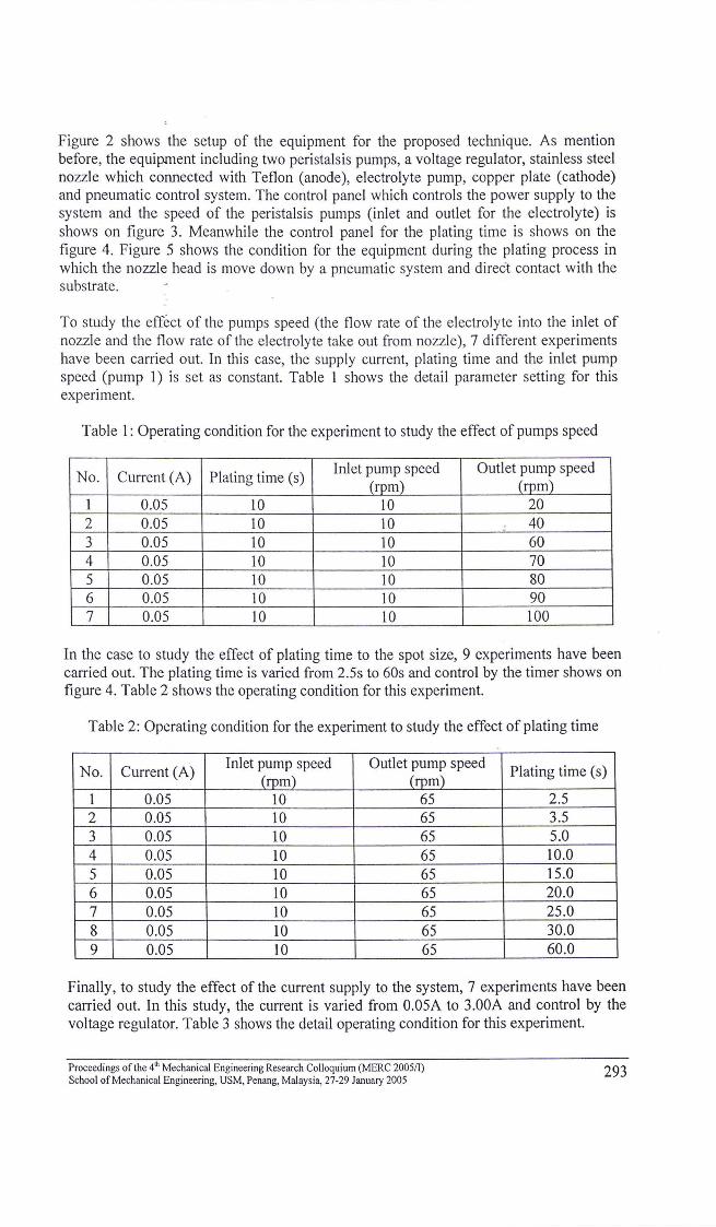
Figure 2 shows the setup of the equipment for the proposed technique. As mentionbefore, the equipment including two peristalsis pumps, a voltage regulator, stainless steelnozzle which connected with Teflon (anode), electrolyte pump, copper plate (cathode)and pneumatic control system. The control panel which controls the power supply to thesystem and the speed of the peristalsis pumps (inlet and outlet for the electrolyte) isshows on figure 3. Meanwhile the control panel for the plating time is shows on thefigure 4. Figure 5 shows the condition for the equipment during the plating process inwhich the nozzle head is move down by a pneumatic system and direCt contact with thesubstrate.
To study the effect of the pumps speed (the flow rate of the electrolyte into the inlet ofnozzle and the flow rate of the electrolyte take out from nozzle), 7 different experimentshave been carried out. In this case, the supply current, plating time and the inlet pumpspeed (pump 1) is set as constant. Table 1 shows the detail parameter setting for thisexperiment.
Table 1: Operating condition for the experiment to study the effect of pumps speed
No. Current (A) Plating time (s)Inlet pump speed Outlet pump speed
(rpm) (rpm)1 0.05 10 10 202 0.05 10 10 403 0.05 10 10 604 0.05 10 10 705 0.05 10 10 806 0.05 10 10 907 0.05 10 10 100
In the case to study the effect of plating time to the spot size, 9 experiments have beencarried out. The plating time is varied from 2.5s to 60s and control by the timer shows onfigure 4. Table 2 shows the operating condition for this experiment.
Table 2: Operating condition for the experiment to study the effect of plating time
No. Current (A)Inlet pump speed Outlet pump speed
Plating time (s)(rpm) (rpm)
1 0.05 10 65 2.52 0.05 10 65 3.53 0.05 10 65 5.04 0.05 10 65 10.05 0.05 10 65 15.06 0.05 10 65 20.07 0.05 10 65 25.08 0.05 10 65 30.09 0.05 10 65 60.0
Finally, to study the effect of the current supply to the system, 7 experiments have beencarried out. In this study, the current is varied from 0.05A to 3.00A and control by thevoltage regulator. Table 3 shows the detail operating condition for this experiment.
Proceedings of the 4th Mechanical Engineering Research Colloquium (MERC 2005fl)School of Mechanical Engineering, USM, Penang, Malaysia, 27-29 January 2005
293

Table 3: Operating condition for the experiment to study the effect of current supply
No. Plating time (s)Inlet pump speed Outlet pump speed
Current (A)(rpm) (rpm)
1 5 10 65 0.052 5 10 65 0.253 5 10 65 0.504 5 10 65 1.005 5 10 65 1.506 5 10 65 2.007 5 10 65 3.00
RESULTS AND DISCUSSION
Spot width Vs Outlet pump speed
3.0000
2.5000
E 2.0000.s£
~ 1.5000.~
~ 1.0000(/)
0.5000
0.0000
o 20 40 60 80
Pump speed (rpm)
100 120
Figure 6: The effect of pumps speed (outlet speed) to the spot size
Spot width Vs Plating time2.2000
2.0000
E 1.8000.s£~ 1.6000.~
g, 1.4000(/)
1.2000
1.0000
o 10 20 30 40Plating time (s)
50 60
Figure 7: The effect of plating time to the spot size
Proceedings of the 4'h Mechanical Engineering Research Colloquium (MERC 200511)School of Mechanical Engineering. USM, Penang. Malaysia, 27-29 January 2005
294

Spot width Vs Current supply1.7500
1.5000
E.s.r:::0 1.2500.~
00-
Cf)
1.0000
0.75000.00 0.50 1.00 1.50 2.00 2.50 3.00 3.50
Current (A)
Figure 8: The effect of current supply to the spot size
Denosit<; area
Figure 9(a)
Deposits area shifted to right
Figure 9(b)
Figure 9 (a): Ideal case for the spot produces by the proposed technique(b): Actual case for the spot produces by the proposed technique
Figure 6 to 8 shows the results obtain from the study of the effect of pumps speed (outletpumps speed), plating time and current supply to the plating system. From figure 6, itshows that with the increases of the outlet pump speed from 20 rpm to 70rpm, the size ofthe spot produce is reducing from around 2.7mm to 1.0mm. This happen due to the forceto take out the electrolyte is increasing when the speed of the outlet pump is increases.With the increasing of the suction force, the surface area of the electrolyte that will directcontact with the substrate will be reducing. Consequently, this causes the reduction of thespot size. However, with the further increases for the outlet pump speed (from 80rpm to100rpm), the shape of the spot produce becomes not more circular and change to theshape of ellipse (increases the spot width to around 1.2mm). This happen due to thesuction force is become greater and causes the electrolyte impingement point shift fromthe center to the right side. As mention before, the proposed technique should have twooutlets to take out the electrolyte and balance the suction force (refer figure 9(a)).However, in this equipment, only one outlet has been created (refer figure 9 (b)). Thusresulting the spot produce having the size more than the expected.
Proceedings of the 4'h Mechanical Engineering Research Colloquium (MERC 2005/1)School of Mechanical Engineering, USM, Penang, Malaysia, 27-29 January 2005
295
Figure 7 shows the results obtain from the study of the effect of plating time. From thegraph, it shows that with the increase of plating time from 2.5s to 3.5s, the spot widthincreases from 1.2mm to 1.4mm and maintain at 1.4mm when the time increases to 5s.The spot size further increases to 1.6mm with the plating time increases to lOs andmaintain with this value with the further increases of the plating time. However, with theplating time further increases to 30s, the spot size is increases to around 2.0mm which is2 times bigger than the size of the Teflon diameter. From the theoretical point of view,the size of spot should maintain around 1.0mm and only the thickness of the spotincreases with the plating time incr~ases. However, in the practical condition, this wasnot happen and the thickness of the spot is increasing ·slowly with the plating time. Fromthe result obtain in the experiment, it can be conclude that the spot size is increases fasterthan the spot thickness with the increases of the plating time. This happen due to thesuction force created by the outlet pump will take out some of the silver deposits on theupper layer if the force created by the outlet pump is greater than the Van der waafforcebetween the silver atom. Beside that, the suction force also might cause the split down ofthe silver layer deposits near to the suction point and this consequently increases the sizeof the spot produce.
Figure 8 shows the results obtain from the study of the effect of current supply. From theresults, it shows that the spot size is maintained on the value of 1.2mm with the increasesof current supply from 0.05A to 0.50A. The further increases of the current supply(l.OOA) cause the spot size increase to 1.5mm and maintain on this level even the currentsupply is further increases. From the results, it can be conclude that current supply isgenerally not much affect to the spot size produce (around O.3mm different with thecurrent increases from 0.05A to 3.00A). However, in term of the point of cost, thesmaller current supply is preferred.
CONCLUSION
The results obtain from the experiments shows that:a. The optimum condition for the pumps speed is:
Inlet pump speed 10 rpmOutlet pump speed 70 rpmWith this speed, the spot with Imm diameter was managed to produce.
b. The optimum condition for the plating time is 2.5s to 3.5s, since with this platingtime, the spot produce having the smaller size (1.2mm). In term of cost, 2.5s ismore preferred.
c. The current supply to the system was not much affect the spot size. Thus asmaller current is preferred due to the smallest the current is use, the lowest theproduction cost can be achieve. In this case, the optimum current supply is 0.05A.
In the future research, the nozzle head with the smaller diameter is plan to use to producethe spot less than I mm. Beside changing the size of the nozzle diameter, the nozzle with2 outlets is prefer to use instead of one for current equipment. With the 2 outlets, morecircular spot is expected can be produce with this technique. The motors with themovement in X and Y direction is proposed to add on the holding table for the substrate.With these 2 motors, the movement of the substrate can be control and any shape of thedeposit area can be draw by controlling the movement of these motors.
Proceedings of the 4th Mechanical Engineering Research Colloquium (MERC 2005/1)School of Mechanical Engineering, USM, Penang, Malaysia, 27-29 January 2005
296