simple, no-math transformer snubber using “quasimodo” test jig
TRANSCRIPT
1
Simple, No-Math Transformer Snubber using “Quasimodo” Test Jig
Mark Johnson
revision A: 07 Sept 2013
Abstract Designing a snubber for a power supply transformer is a lengthy process, requiring both measurements and calculations. Usually a sinewave generator is connected to the transformer secondary, with primary shorted. The sinewave frequency is swept, in search of an impedance peak. Next, a known-value capacitor is connected across the secondary, and a second frequency sweep obtains a second impedance peak at a second, lower, frequency. The two measured peak-impedance frequencies provide two equations in two unknowns (inductance and capacitance), which are algebraically solved. Finally the extracted inductance and capacitance are inserted into the damping equation for this second-order RLC circuit, and a snubber resistance RS is calculated which provides the desired damping factor. It is assumed that transformer inductance is approximately constant across frequency, which is convenient for the math but unfortunately not true in real transformers. This note presents another way to design a snubber, which requires no calculations, no assumptions, and only a single measurement. Rather than measuring the transformer parameters and then calculating the snubber, this procedure places an actual snubber across the transformer, observes transformer ringing directly, and adjusts the snubber until ringing is damped into non-existence. The snubber value which successfully damps the ringing is then transferred to the final product design.
Introduction
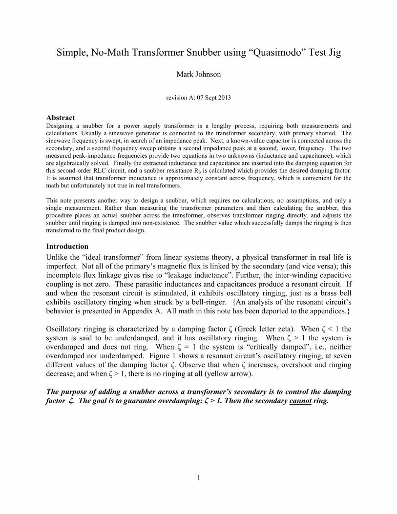
Unlike the “ideal transformer” from linear systems theory, a physical transformer in real life is imperfect. Not all of the primary’s magnetic flux is linked by the secondary (and vice versa); this incomplete flux linkage gives rise to “leakage inductance”. Further, the inter-winding capacitive coupling is not zero. These parasitic inductances and capacitances produce a resonant circuit. If and when the resonant circuit is stimulated, it exhibits oscillatory ringing, just as a brass bell exhibits oscillatory ringing when struck by a bell-ringer. An analysis of the resonant circuit’s behavior is presented in Appendix A. All math in this note has been deported to the appendices. Oscillatory ringing is characterized by a damping factor ζ (Greek letter zeta). When ζ < 1 the system is said to be underdamped, and it has oscillatory ringing. When ζ > 1 the system is overdamped and does not ring. When ζ = 1 the system is “critically damped”, i.e., neither overdamped nor underdamped. Figure 1 shows a resonant circuit’s oscillatory ringing, at seven different values of the damping factor ζ. Observe that when ζ increases, overshoot and ringing decrease; and when ζ > 1, there is no ringing at all (yellow arrow). The purpose of adding a snubber across a transformer’s secondary is to control the damping factor ζ. The goal is to guarantee overdamping: ζ > 1. Then the secondary cannot ring.
2
Figure 1.
The damping factor ζ is inversely proportional to the resonant circuit’s quality factor Q, which you may have encountered when studying for a ham radio license:
12ζ
Yes, that really is a Greek zeta in the denominator. For some reason, Microsoft Word renders zeta in a different font for equations, than it renders for body text. I apologize for this peculiarity.
Quasimodo the bell-ringer
Instead of measuring the transformer and then calculating the snubber, why not simply connect an adjustable snubber across the secondary, stimulate the resonant circuit to make it ring, and then adjust the snubber until you find a setting where all ringing is perfectly damped? Just smack the bell and find a snubber that prevents it from ringing! With apologies to Victor Hugo, I present here a simple test jig which does exactly that, called Quasimodo the bell-ringer.
3
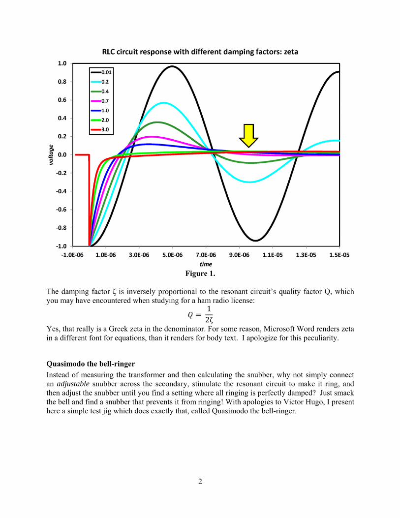
Figure 2.
The Quasimodo concept is shown in Figure 2. R1, R2, and switch SW1 form a pulse generator with extremely low output impedance at the high-to-low transition (when SW1 closes). LT represents the transformer secondary’s leakage inductance, and CT represents the secondary’s inter-winding capacitance. The transformer’s primary is shorted. Capacitor C2 injects a high-to-low voltage step into the resonant circuit. C2 is the hammer which strikes the bell. For now, we’ll pretend C2 << CT. Please note that Quasimodo is AC coupled to the transformer; there is no DC current path, and no way for the test jig to DC-magnetize the transformer core.
Figure 3.
Figure 3 shows Quasimodo driving a typical transformer secondary (with primary shorted). Oscilloscope channel 1 is the Quasimodo stimulus signal (R1-C2 junction), and channel 2 is the transformer secondary (CT-LT junction). The bell-ringer smacks the bell, which exhibits classical damped oscillation. In Fig.3 Quasimodo was powered by a +15V supply; the amplitude of oscillatory ringing is ± 11 volts. By the way, the damping factor ζ in Figure 3 is approx. 0.09. Appendix B shows how to calculate ζ from a plot of damped oscillatory ringing.
4
Detailed circuit design
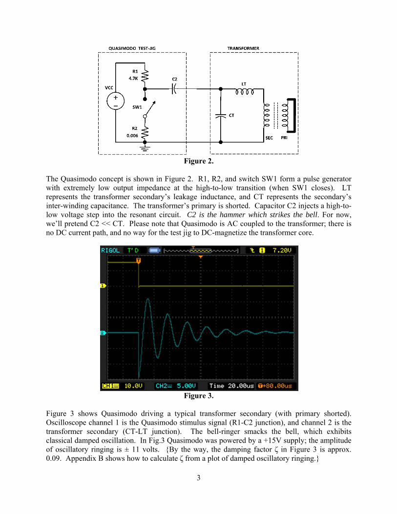
Figure 4 shows a representative circuit schematic of a Quasimodo test jig. R2 and SW1 in Fig.2 have been replaced by M1, a power MOSFET whose RDS(on) sets the output impedance. The large gate capacitance of the MOSFET is driven by a high (6 amps!) output current CMOS IC. A logic level gate MOSFET was selected, to ensure that Quasimodo will correctly operate at supply voltages below 2.7V. The 120Hz oscillator uses a CMOS 555 with rail-to-rail output swing, for the same reason: a non-CMOS 555 chip’s output only swings to VCC – 2VBE, which spoils low voltage operation. Injection capacitor C2 is socketed, with provision for any lead spacing between 0.2 inches and 0.7 inches (5.0 to 17.5 mm). This makes it easy to swap different capacitors into the C2 position. Snubber capacitor C3 is socketed for the same reason. Snubber resistor RV1, a 25-turn trimmer potentiometer, provides fine-grained adjustment to achieve precise damping. RV1 is also socketed, so you can remove it and measure its resistance.
Figure 4.
5
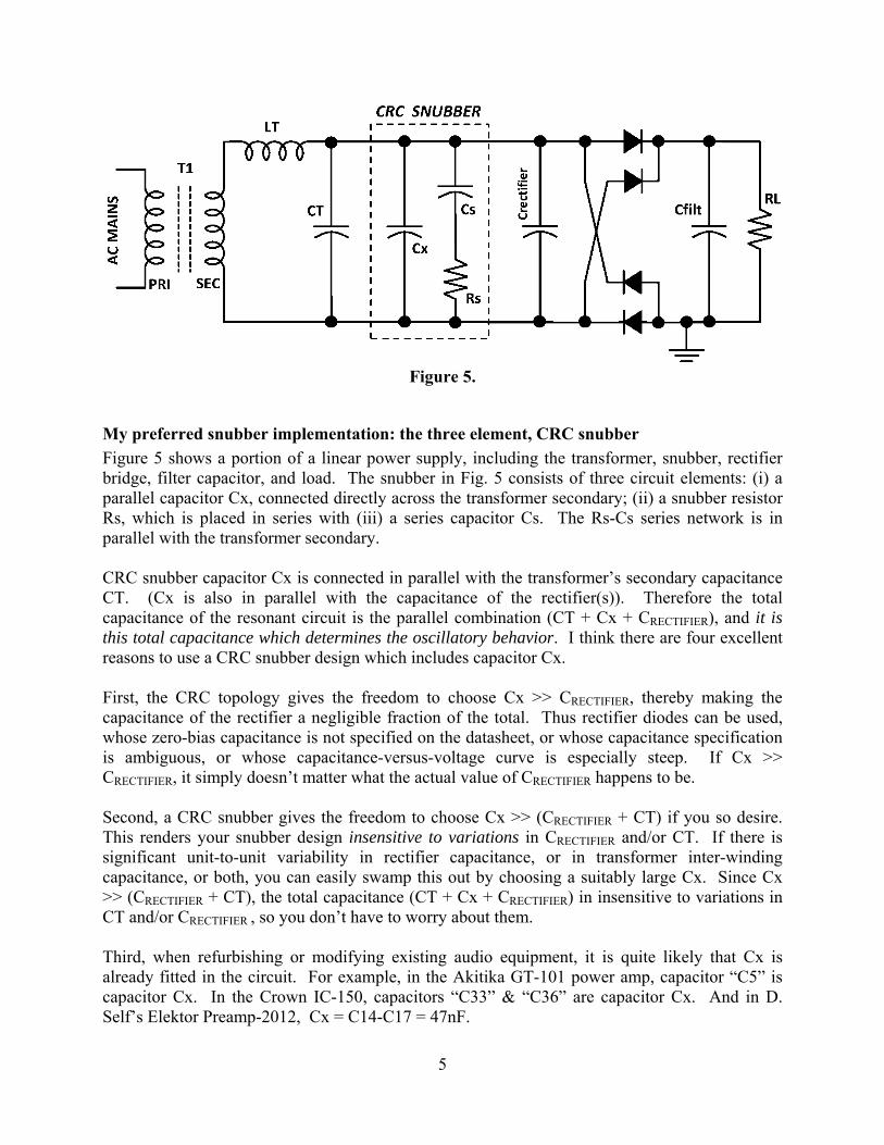
Figure 5.
My preferred snubber implementation: the three element, CRC snubber
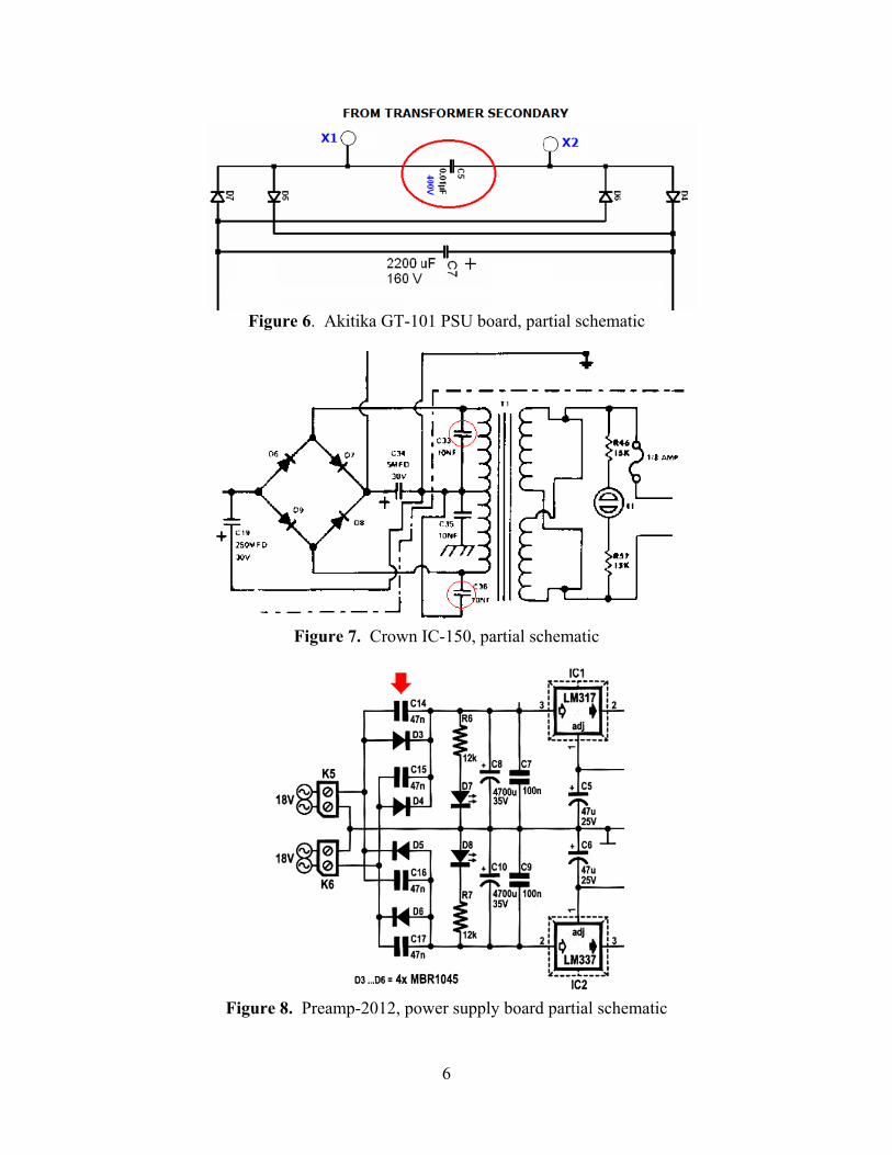
Figure 5 shows a portion of a linear power supply, including the transformer, snubber, rectifier bridge, filter capacitor, and load. The snubber in Fig. 5 consists of three circuit elements: (i) a parallel capacitor Cx, connected directly across the transformer secondary; (ii) a snubber resistor Rs, which is placed in series with (iii) a series capacitor Cs. The Rs-Cs series network is in parallel with the transformer secondary. CRC snubber capacitor Cx is connected in parallel with the transformer’s secondary capacitance CT. (Cx is also in parallel with the capacitance of the rectifier(s)). Therefore the total capacitance of the resonant circuit is the parallel combination (CT + Cx + CRECTIFIER), and it is this total capacitance which determines the oscillatory behavior. I think there are four excellent reasons to use a CRC snubber design which includes capacitor Cx. First, the CRC topology gives the freedom to choose Cx >> CRECTIFIER, thereby making the capacitance of the rectifier a negligible fraction of the total. Thus rectifier diodes can be used, whose zero-bias capacitance is not specified on the datasheet, or whose capacitance specification is ambiguous, or whose capacitance-versus-voltage curve is especially steep. If Cx >> CRECTIFIER, it simply doesn’t matter what the actual value of CRECTIFIER happens to be. Second, a CRC snubber gives the freedom to choose Cx >> (CRECTIFIER + CT) if you so desire. This renders your snubber design insensitive to variations in CRECTIFIER and/or CT. If there is significant unit-to-unit variability in rectifier capacitance, or in transformer inter-winding capacitance, or both, you can easily swamp this out by choosing a suitably large Cx. Since Cx >> (CRECTIFIER + CT), the total capacitance (CT + Cx + CRECTIFIER) in insensitive to variations in CT and/or CRECTIFIER , so you don’t have to worry about them. Third, when refurbishing or modifying existing audio equipment, it is quite likely that Cx is already fitted in the circuit. For example, in the Akitika GT-101 power amp, capacitor “C5” is capacitor Cx. In the Crown IC-150, capacitors “C33” & “C36” are capacitor Cx. And in D. Self’s Elektor Preamp-2012, Cx = C14-C17 = 47nF.
6
Figure 6. Akitika GT-101 PSU board, partial schematic
Figure 7. Crown IC-150, partial schematic
Figure 8. Preamp-2012, power supply board partial schematic
7
Fourth, the CRC snubber topology explicitly includes Quasimodo’s injection capacitor C2: Cx is C2, and C2 is Cx (see Figures 4 and 5). Thus Quasimodo will directly produce an optimized CRC snubber without requiring any further calculations or component changes. When a CRC snubber is used, we don’t need to pretend that Quasimodo’s C2 is much much smaller than CT (see the discussion of Figure 2, above).
Guidelines for selecting CRC snubber components
I recommend Cx = 10 nF, Cs = 150 nF, RV1 = 25 turn, 1K trimmer, at least as a starting point for further experimentation. These values have produced reasonable snubbers in my experience, across a wide variety of transformers. I prefer to use metallized film capacitor types for Cx and Cs, because of their excellent dissipation factor (tan δ); the EPCOS B32529 series is a favorite. Most rectifiers have a zero-bias capacitance between 50 pF and 300 pF. Four of them in parallel gives 200 to 1200 pF, so a choice of Cx = 10nF ensures Cx >> CRECTIFIER . Although the details are outside the scope of this “no-math” note, I have measured/estimated the secondary capacitance CT of several power transformers, using multivariate least squares software to fit a six parameter model. The largest secondary capacitance I’ve seen to date is CT = 1.6 nF. Thus choosing Cx = 10nF gives the desired result: Cx >> (CT + CRECTIFIER), even in the worst case scenario. Cs should be larger than Cx the final paragraph of Appendix A explains why, and in my own audio work I usually select Cs to be about 15X greater than Cx. When fitting a snubber to existing equipment that already has a Cx installed, I would of course install that same value of Cx into the Quasimodo test jig, and also install a Cs which is 10X or 20X larger. In the final product design Rs is a fixed resistor, replacing trimmer RV1. A quick SPICE simulation sinewave source (SecondaryVrms*1.414) driving the CRC snubber will tell you the power dissipated in Rs. Or you can draw the ac circuit and use math to compute the power dissipated in Rs. For secondary voltages below approx. 75 volts RMS, and for typical snubber resistor values (50Ω < Rs < 500Ω), the average power dissipated in Rs will be less than 70 milliwatts. Still, I prefer to fit an 0.5W or 0.6W fixed resistor, giving a comfortable safety margin. Some authors suggest using a carbon composition resistor for Rs, but these can be difficult to source in E48 or E96 values, at 0.5 watts. I often use an 0.5W metal film part.
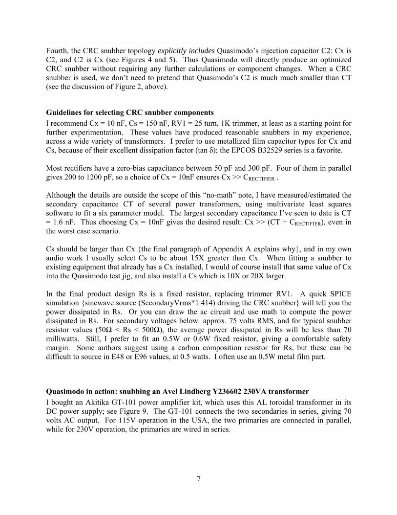
Quasimodo in action: snubbing an Avel Lindberg Y236602 230VA transformer
I bought an Akitika GT-101 power amplifier kit, which uses this AL toroidal transformer in its DC power supply; see Figure 9. The GT-101 connects the two secondaries in series, giving 70 volts AC output. For 115V operation in the USA, the two primaries are connected in parallel, while for 230V operation, the primaries are wired in series.
8
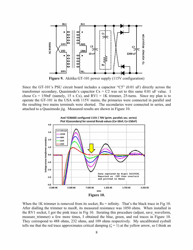
Figure 9. Akitika GT-101 power supply (115V configuration)
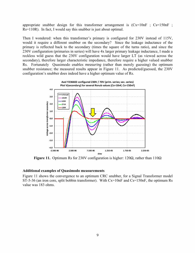
Since the GT-101’s PSU circuit board includes a capacitor “C5” (0.01 uF) directly across the transformer secondary, Quasimodo’s capacitor Cx = C2 was set to this same 0.01 uF value. I chose Cs = 150nF (namely, 15 x Cx), and RV1 = 1K trimmer, 25-turns. Since my plan is to operate the GT-101 in the USA with 115V mains, the primaries were connected in parallel and the resulting two mains terminals were shorted. The secondaries were connected in series, and attached to a Quasimodo jig. Measured results are shown in Figure 10.
Figure 10.
When the 1K trimmer is removed from its socket, Rs = infinity. That’s the black trace in Fig 10. After dialling the trimmer to maxR, its measured resistance was 1050 ohms. When installed in the RV1 socket, I got the pink trace in Fig 10. Iterating this procedure (adjust, save_waveform, measure_trimmer) a few more times, I obtained the blue, green, and red traces in Figure 10. They correspond to 488 ohms, 232 ohms, and 109 ohms respectively. My uncalibrated eyeball tells me that the red trace approximates critical damping (ζ = 1) at the yellow arrow, so I think an
9
appropriate snubber design for this transformer arrangement is (Cx=10nF ; Cs=150nF ; Rs=110R). In fact, I would say this snubber is just about optimal. Then I wondered: when this transformer’s primary is configured for 230V instead of 115V, would it require a different snubber on the secondary? Since the leakage inductance of the primary is reflected back to the secondary (times the square of the turns ratio), and since the 230V configuration (primaries in series) will have 4x larger primary leakage inductance, I made a reckless wild guess that the 230V configuration would have larger LT (as viewed across the secondary), therefore larger characteristic impedance, therefore require a higher valued snubber Rs. Fortunately Quasimodo enables measuring (rather than merely guessing) the optimum snubber resistance; the measured results appear in Figure 11. As predicted/guessed, the 230V configuration’s snubber does indeed have a higher optimum value of Rs.
Figure 11. Optimum Rs for 230V configuration is higher: 120Ω, rather than 110Ω
Additional examples of Quasimodo measurements
Figure 11 shows the convergence to an optimum CRC snubber, for a Signal Transformer model ST-5-36 (an iron core, split bobbin transformer). With Cx=10nF and Cs=150nF, the optimum Rs value was 183 ohms.
10
Figure 11.
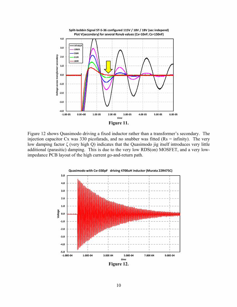
Figure 12 shows Quasimodo driving a fixed inductor rather than a transformer’s secondary. The injection capacitor Cx was 330 picofarads, and no snubber was fitted (Rs = infinity). The very low damping factor ζ (very high Q) indicates that the Quasimodo jig itself introduces very little additional (parasitic) damping. This is due to the very low RDS(on) MOSFET, and a very low-impedance PCB layout of the high current go-and-return path.
Figure 12.
11
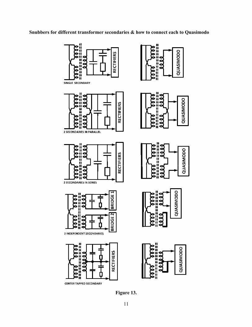
Snubbers for different transformer secondaries & how to connect each to Quasimodo
Figure 13.
12
The first three configurations are straightforward. In each case the downstream power supply circuitry connects to the transformer at exactly two nodes. The snubber is connected between these two nodes. Thus the Quasimodo test jig, which is really nothing but a snubber, is also connected to these same two circuit nodes The dual secondary transformer with independent secondary circuits (4th row), connects downstream at four circuit nodes and it needs two snubbers. One snubber for secondary circuit Top, and another snubber for secondary circuit Bottom. Short the Bottom secondary winding when connecting the Top winding to Quasimodo, and vice versa. I only test one winding, and then assume the other is approximately identical. A skeptic would run Quasimodo twice. The center tapped transformer (5th row) connects to the downstream power supply at three circuit nodes. It needs two snubbers: a first snubber between the top winding and the center-tap; and a second snubber between the bottom winding and the center tap. To optimize the snubber, short one of the secondary windings to the center tap, and connect the other winding + the center tap to Quasimodo. A skeptic would assume the two windings are not identical, and so a skeptic would optimize the top snubber, then separately optimize the bottom snubber. I only run Quasimodo on one winding, and then use those values for both. I’m not a skeptic.
Triggering the oscilloscope
You can get wonderfully clean and stable oscilloscope traces from Quasimodo if you use a two channel scope. Referring to Figure 4, channel 1 connects to the MOSFET’s drain pin (the left hand side of C2), and Ch.1 triggers the scope from a very sharp, very clean falling edge. Channel 2 connects to the transformer secondary (the right hand side of C2), and displays the oscillatory ringing. This is exactly the setup used to create the scope photo of Figure 3. Hint#1: If you provide a socket for C2, and if this socket has numerous holes to accommodate several capacitor lead spacings, you can plug ~ 1cm pieces of hookup wire into unused socket holes and attach your scope probes to them. Hint #2: after adjusting the trigger level on channel 1 and getting stable waveforms, you can set the scope so it only displays channel 2. This unclutters the screen. If you only have a single channel scope (or if you can only find one working scope probe!), you can view the transformer secondary waveform and trigger on it: Figure 3 illustrates. With your probe connected to the transformer node (bottom trace), trigger on the falling edge and set the trigger level at the very bottom of the initial falling edge. In Figure 3 that would be about two and a half divisions below the baseline; i.e. about (-2.5 x 5V/div) = -12.5 volts. It won’t be quite as clean as the two channel setup, but it should be useable.
The two element, RC snubber (non preferred)
Some people choose to omit capacitor Cx from Figure 5, which produces a two element “RC” snubber consisting of Rs and Cs. This snubber design can be made to work, but I find it inferior to the CRC snubber for the four reasons discussed previously. Nevertheless, if you absolutely insist upon building a two element snubber, Quasimodo can still be a useful tool.
13
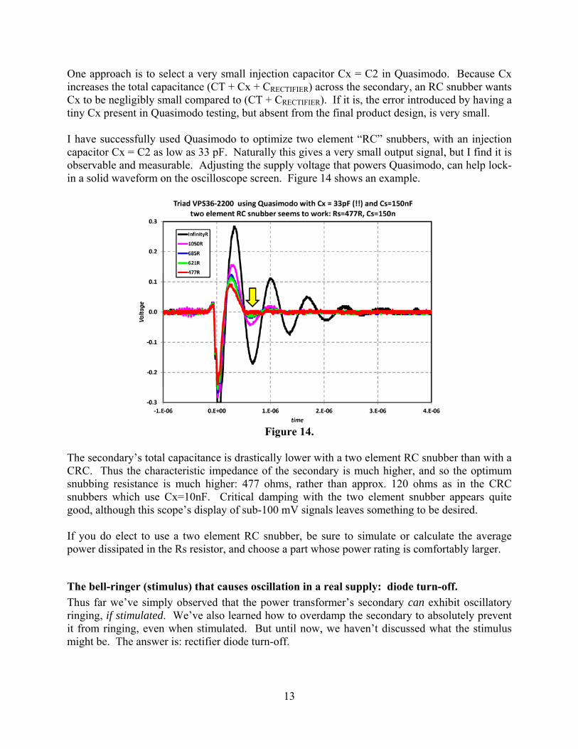
One approach is to select a very small injection capacitor Cx = C2 in Quasimodo. Because Cx increases the total capacitance (CT + Cx + CRECTIFIER) across the secondary, an RC snubber wants Cx to be negligibly small compared to (CT + CRECTIFIER). If it is, the error introduced by having a tiny Cx present in Quasimodo testing, but absent from the final product design, is very small. I have successfully used Quasimodo to optimize two element “RC” snubbers, with an injection capacitor Cx = C2 as low as 33 pF. Naturally this gives a very small output signal, but I find it is observable and measurable. Adjusting the supply voltage that powers Quasimodo, can help lock-in a solid waveform on the oscilloscope screen. Figure 14 shows an example.
Figure 14.
The secondary’s total capacitance is drastically lower with a two element RC snubber than with a CRC. Thus the characteristic impedance of the secondary is much higher, and so the optimum snubbing resistance is much higher: 477 ohms, rather than approx. 120 ohms as in the CRC snubbers which use Cx=10nF. Critical damping with the two element snubber appears quite good, although this scope’s display of sub-100 mV signals leaves something to be desired. If you do elect to use a two element RC snubber, be sure to simulate or calculate the average power dissipated in the Rs resistor, and choose a part whose power rating is comfortably larger.
The bell-ringer (stimulus) that causes oscillation in a real supply: diode turn-off.
Thus far we’ve simply observed that the power transformer’s secondary can exhibit oscillatory ringing, if stimulated. We’ve also learned how to overdamp the secondary to absolutely prevent it from ringing, even when stimulated. But until now, we haven’t discussed what the stimulus might be. The answer is: rectifier diode turn-off.
14
The transformer secondary’s sinusoidal output voltage is applied to the rectifier(s) + filter capacitor(s). When the secondary voltage exceeds Vcap + Vdiode, the rectifier turns on and the transformer recharges the filter capacitor. After the sinewave crests and the secondary voltage begins to fall, eventually it falls below (Vcap + Vdiode) and the rectifier turns off. Unfortunately, some rectifier diodes have uncontrolled or poorly-controlled turn-off characteristics, and they turn off extremely rapidly. Particularly troublesome are rectifiers that turn off “abruptly”, i.e., with very large dI/dt. Abrupt diode turn-off with extremely large dI/dt is the stimulus that causes transformer secondary circuits to begin oscillatory ringing. Large dI/dt immediately manifests as a large voltage across the leakage inductance (recall: V = L dI/dt), and this large voltage-step is the start of the oscillatory ringing waveform. “Aha!” people have exclaimed, “then let’s find and use rectifier diodes whose turn-off is guaranteed to have small dI/dt! Our transformer bell will never ring, because it will never be struck!” Such rectifier diodes do exist, and are guaranteed by their manufacturer’s data sheets to have small dI/dt at turn-off. They are called “Soft Recovery” diodes, and the newest models have a datasheet specification named “softness factor” (Tb / Ta) which quantifies just how low their dI/dt actually is. Beware, soft recovery diodes often have very large forward voltage drop -- sometimes higher than 2.5 volts -- so calculate your supply voltage headroom (margin) very carefully. Also calculate your rectifier power dissipation; you may need a significantly larger heatsink for soft recovery diodes than for standard (or Schottky) diodes with low Vfwd. Philosophically, I prefer to employ a belt-and-suspenders approach: prevent transformer secondary ringing, two different ways. First, snub (overdamp) the secondary so it cannot possibly ring, even if stimulated. Second, use soft recovery rectifiers so the secondary cannot possibly be stimulated. Especially in a DIY piece of equipment where the cost of a CRC snubber is completely negligible, I think it makes no sense at all to ever omit snubbers. Fairchild “Stealth” soft recovery rectifiers are slightly more expensive than garden variety silicon bridge rectifier assemblies, and Vishay “Hex FRED” diodes are yet more expensive. But even these are only $2.28 in quantity ten; to purchase 8 of them for a pair of fully independent bridge rectifiers on the rails of a DIY power amp, would cost only $18.25. Less than two admission tickets to the cinema. DIY project budgets can afford this. In the competitive arena of commercial products designed to a price point, I think snubbers (made of low-tech passive components) are significantly cheaper to source and implement, than new, modern, soft recovery rectifiers. So if it were my task to build and sell power amps at less than $2.00 per RMS watt, I’d probably put the snubbers in and leave the soft recovery diodes out.
Other test equipment similar to Quasimodo
Several weeks after I built and started to use the first version of Quasimodo, I discovered that other people had done very similar things, long ago. Most notably, the Boonton Radio Corporation sold a “Q Meter” which measures the quality factor Q of inductors and transformers used in radio frequency applications. Its principle of operation is the same as Quasimodo’s: the Q-Meter drives the inductor or transformer, at frequencies near self-resonance, from an extremely low output impedance signal generator. Monitoring the waveform across the inductor with a high input impedance amplifier (Quasimodo uses an oscilloscope), the Q-Meter measures damping and thus Q. Recall that Q = 1/(2×ζ).
15
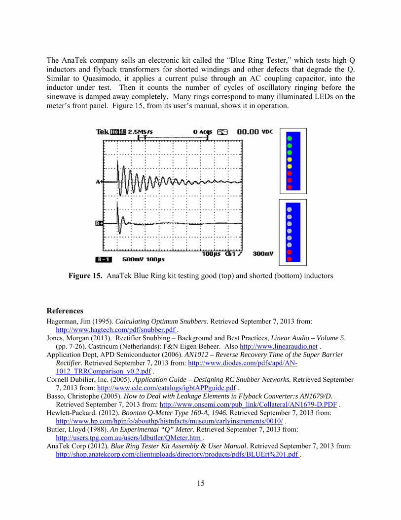
The AnaTek company sells an electronic kit called the “Blue Ring Tester,” which tests high-Q inductors and flyback transformers for shorted windings and other defects that degrade the Q. Similar to Quasimodo, it applies a current pulse through an AC coupling capacitor, into the inductor under test. Then it counts the number of cycles of oscillatory ringing before the sinewave is damped away completely. Many rings correspond to many illuminated LEDs on the meter’s front panel. Figure 15, from its user’s manual, shows it in operation.
Figure 15. AnaTek Blue Ring kit testing good (top) and shorted (bottom) inductors
References Hagerman, Jim (1995). Calculating Optimum Snubbers. Retrieved September 7, 2013 from:
http://www.hagtech.com/pdf/snubber.pdf . Jones, Morgan (2013). Rectifier Snubbing – Background and Best Practices, Linear Audio – Volume 5,
(pp. 7-26). Castricum (Netherlands): F&N Eigen Beheer. Also http://www.linearaudio.net . Application Dept, APD Semiconductor (2006). AN1012 – Reverse Recovery Time of the Super Barrier
Rectifier. Retrieved September 7, 2013 from: http://www.diodes.com/pdfs/apd/AN-1012_TRRComparison_v0.2.pdf .
Cornell Dubilier, Inc. (2005). Application Guide – Designing RC Snubber Networks. Retrieved September 7, 2013 from: http://www.cde.com/catalogs/igbtAPPguide.pdf .
Basso, Christophe (2005). How to Deal with Leakage Elements in Flyback Converter:s AN1679/D. Retrieved September 7, 2013 from: http://www.onsemi.com/pub_link/Collateral/AN1679-D.PDF .
Hewlett-Packard. (2012). Boonton Q-Meter Type 160-A, 1946. Retrieved September 7, 2013 from: http://www.hp.com/hpinfo/abouthp/histnfacts/museum/earlyinstruments/0010/ .
Butler, Lloyd (1988). An Experimental “Q” Meter. Retrieved September 7, 2013 from: http://users.tpg.com.au/users/ldbutler/QMeter.htm .
AnaTek Corp (2012). Blue Ring Tester Kit Assembly & User Manual. Retrieved September 7, 2013 from: http://shop.anatekcorp.com/clientuploads/directory/products/pdfs/BLUErt%201.pdf .
16
Appendix A: Analysis of an RLC resonant circuit
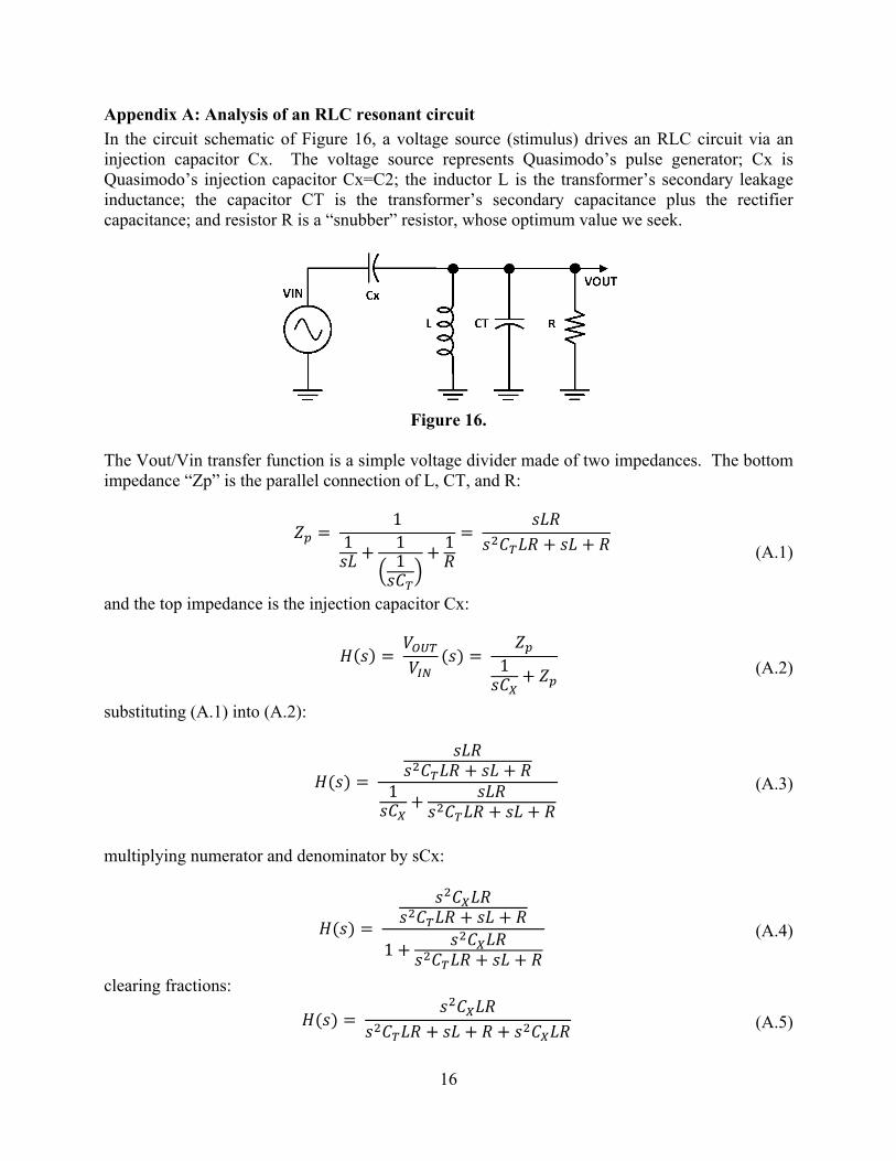
In the circuit schematic of Figure 16, a voltage source (stimulus) drives an RLC circuit via an injection capacitor Cx. The voltage source represents Quasimodo’s pulse generator; Cx is Quasimodo’s injection capacitor Cx=C2; the inductor L is the transformer’s secondary leakage inductance; the capacitor CT is the transformer’s secondary capacitance plus the rectifier capacitance; and resistor R is a “snubber” resistor, whose optimum value we seek.
Figure 16.
The Vout/Vin transfer function is a simple voltage divider made of two impedances. The bottom impedance “Zp” is the parallel connection of L, CT, and R:
1
1 11
1(A.1)
and the top impedance is the injection capacitor Cx:
1 (A.2)
substituting (A.1) into (A.2):
1 (A.3)
multiplying numerator and denominator by sCx:
1(A.4)
clearing fractions:
(A.5)
17
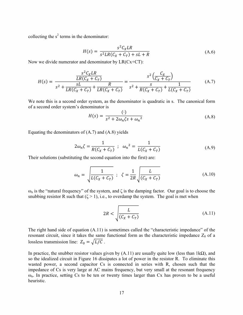
collecting the s2 terms in the denominator:
(A.6)
Now we divide numerator and denominator by LR(Cx+CT):
1 (A.7)
We note this is a second order system, as the denominator is quadratic in s. The canonical form of a second order system’s denominator is
∙2 (A.8)
Equating the denominators of (A.7) and (A.8) yields
21
;1
(A.9)
Their solutions (substituting the second equation into the first) are:
1
;12
(A.10)
ωn is the “natural frequency” of the system, and ζ is the damping factor. Our goal is to choose the snubbing resistor R such that (ζ > 1), i.e., to overdamp the system. The goal is met when
2 (A.11)
The right hand side of equation (A.11) is sometimes called the “characteristic impedance” of the resonant circuit, since it takes the same functional form as the characteristic impedance Z0 of a lossless transmission line: / . In practice, the snubber resistor values given by (A.11) are usually quite low (less than 1kΩ), and so the idealized circuit in Figure 16 dissipates a lot of power in the resistor R. To eliminate this wasted power, a second capacitor Cs is connected in series with R, chosen such that the impedance of Cs is very large at AC mains frequency, but very small at the resonant frequency ωn. In practice, setting Cs to be ten or twenty times larger than Cx has proven to be a useful heuristic.
18
Appendix B: Estimating ζ of a resonant circuit from its time domain waveform
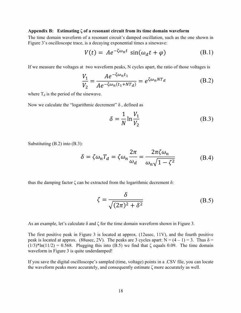
The time domain waveform of a resonant circuit’s damped oscillation, such as the one shown in Figure 3’s oscilloscope trace, is a decaying exponential times a sinewave:
sin (B.1) If we measure the voltages at two waveform peaks, N cycles apart, the ratio of those voltages is
(B.2)
where Td is the period of the sinewave. Now we calculate the “logarithmic decrement” δ , defined as
1ln (B.3)
Substituting (B.2) into (B.3):
2 2
1 (B.4)
thus the damping factor ζ can be extracted from the logarithmic decrement δ:
2(B.5)
As an example, let’s calculate δ and ζ for the time domain waveform shown in Figure 3. The first positive peak in Figure 3 is located at approx. (12usec, 11V), and the fourth positive peak is located at approx. (88usec, 2V). The peaks are 3 cycles apart: N = (4 – 1) = 3. Thus δ = (1/3)*ln(11/2) = 0.568. Plugging this into (B.5) we find that ζ equals 0.09. The time domain waveform in Figure 3 is quite underdamped! If you save the digital oscilloscope’s sampled (time, voltage) points in a .CSV file, you can locate the waveform peaks more accurately, and consequently estimate ζ more accurately as well.
19
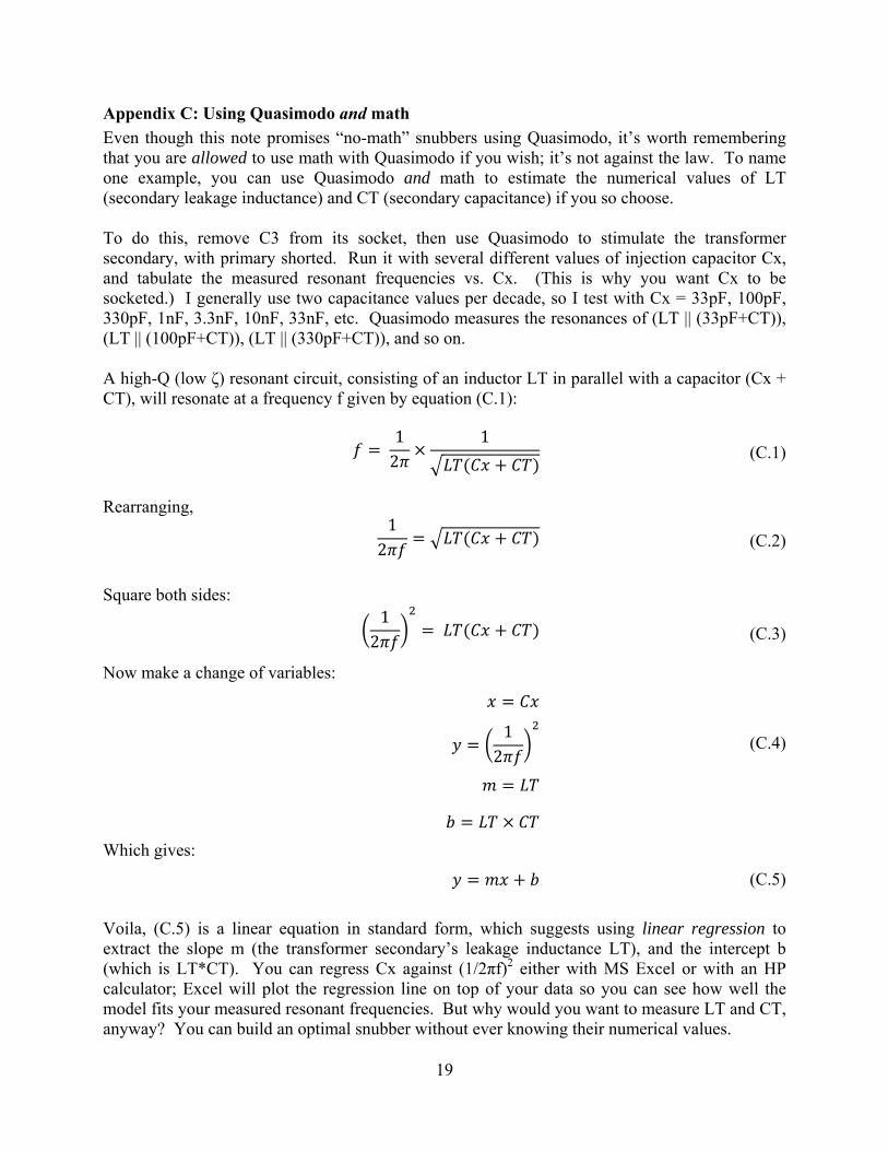
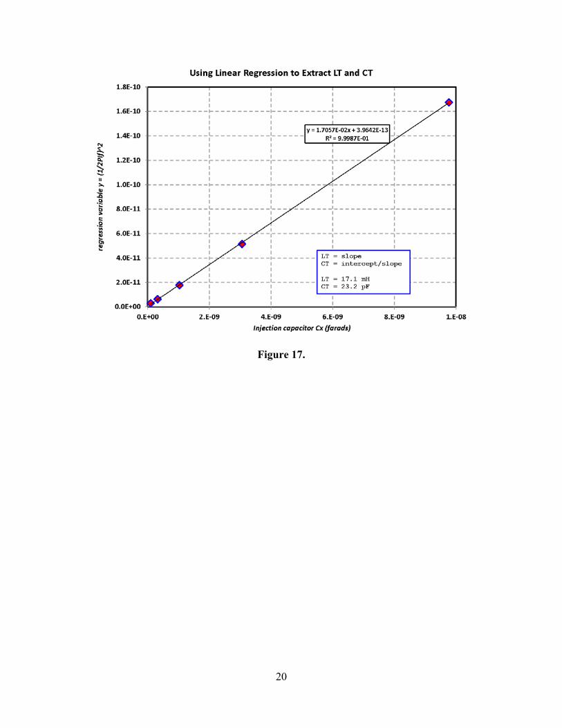
Appendix C: Using Quasimodo and math
Even though this note promises “no-math” snubbers using Quasimodo, it’s worth remembering that you are allowed to use math with Quasimodo if you wish; it’s not against the law. To name one example, you can use Quasimodo and math to estimate the numerical values of LT (secondary leakage inductance) and CT (secondary capacitance) if you so choose. To do this, remove C3 from its socket, then use Quasimodo to stimulate the transformer secondary, with primary shorted. Run it with several different values of injection capacitor Cx, and tabulate the measured resonant frequencies vs. Cx. (This is why you want Cx to be socketed.) I generally use two capacitance values per decade, so I test with Cx = 33pF, 100pF, 330pF, 1nF, 3.3nF, 10nF, 33nF, etc. Quasimodo measures the resonances of (LT || (33pF+CT)), (LT || (100pF+CT)), (LT || (330pF+CT)), and so on. A high-Q (low ζ) resonant circuit, consisting of an inductor LT in parallel with a capacitor (Cx + CT), will resonate at a frequency f given by equation (C.1):
12
1(C.1)
Rearranging,
12 (C.2)
Square both sides:
12 (C.3)
Now make a change of variables:
12
(C.4)
Which gives:
(C.5)
Voila, (C.5) is a linear equation in standard form, which suggests using linear regression to extract the slope m (the transformer secondary’s leakage inductance LT), and the intercept b (which is LT*CT). You can regress Cx against (1/2πf)2 either with MS Excel or with an HP calculator; Excel will plot the regression line on top of your data so you can see how well the model fits your measured resonant frequencies. But why would you want to measure LT and CT, anyway? You can build an optimal snubber without ever knowing their numerical values.
20
Figure 17.
21
Appendix D: Verifying transformer winding polarity
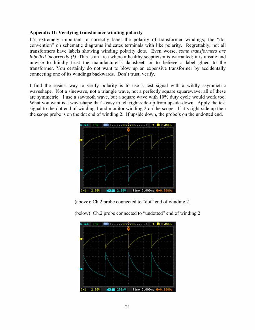
It’s extremely important to correctly label the polarity of transformer windings; the “dot convention” on schematic diagrams indicates terminals with like polarity. Regrettably, not all transformers have labels showing winding polarity dots. Even worse, some transformers are labelled incorrectly (!) This is an area where a healthy scepticism is warranted; it is unsafe and unwise to blindly trust the manufacturer’s datasheet, or to believe a label glued to the transformer. You certainly do not want to blow up an expensive transformer by accidentally connecting one of its windings backwards. Don’t trust; verify. I find the easiest way to verify polarity is to use a test signal with a wildly asymmetric waveshape. Not a sinewave, not a triangle wave, not a perfectly square squarewave; all of these are symmetric. I use a sawtooth wave, but a square wave with 10% duty cycle would work too. What you want is a waveshape that’s easy to tell right-side-up from upside-down. Apply the test signal to the dot end of winding 1 and monitor winding 2 on the scope. If it’s right side up then the scope probe is on the dot end of winding 2. If upside down, the probe’s on the undotted end.
(above): Ch.2 probe connected to “dot” end of winding 2
(below): Ch.2 probe connected to “undotted” end of winding 2
22
Appendix E: Quasimodo test jig design notes
Quasimodo is a testbench tool, and I encourage readers to modify and enhance it however they see fit. The design presented in this note probably includes a few decisions that others would have made differently. Change it! Tweak Quasimodo to suit your own needs. For example, I deliberately built my Quasimodo jig to be powered from an external power supply with adjustable voltage. I wanted to have the flexibility to dial the supply voltage, from very low (2.5 volts) to very high (18 volts, limited by VGSmax of the MOSFET). You may not need or want a supply range this large, and so you might build a Quasimodo test jig with a “barrel jack” connector for the power input, which comes from an AC adapter Wall Wart. Or you might run it from a 9 volt battery clip. If you don’t need or want low voltage operation, you can select a standard gate threshold MOSFET instead of the logic gate threshold NTD4906 that I used. By the way, even though the NTD4906 is in an IPAK package (0.090 inch lead spacing), I laid out my thru-hole PCBoard with a TO220 footprint (0.100 inch lead spacing). This gives the flexibility to substitute other MOSFETs if desired. It’s easy to gently spread out the leads of an IPAK to fit it into the TO220 footprint. I’ve also built Quasimodo on a surface mount PCBoard. I selected the 8-lead SOIC package for the LMC555, and for the FET gate driver IC, and for the power MOSFET itself. The SO8 is relatively forgiving and easy to solder by hand, since it has exposed leads. Also for ease of hand soldering, I chose 1206 sized resistors and capacitors. People with steadier hands and younger eyes than mine, may choose to use smaller parts and perhaps even reflow-only packages for their SMD Quasimodo. For ease of pick-and-place with SMD capacitors (which are unmarked!), I chose a single capacitance value to be used in every capacitor position: 0.15 microfarads. The oscillator timing capacitor is 0.15uF, the 555 control voltage bypass capacitor on pin 5 is 0.15uF, and all seven of the supply bypass capacitors are 0.15uF. With only one value capacitor for the entire board, it’s impossible to solder a wrong value cap in the wrong position. I plan to upload the schematics, Bill Of Materials, and PCB fab-house “Gerber” files of my V.3 (SMD) and V.4 (thru hole) circuit board designs, to the www.diyaudio.com website. Search there for Quasimodo. You may not agree with some of the choices I made:
Schottky diode in series with +Vsupply, protects against reverse polarity Many VCC/GND ceramic bypass capacitors & 220 uF electrolytic bypass caps Power-on indicator LED DIPswitch that changes oscillator frequency (thru-hole PCB only; the switch is HUGE) Alligator-clip connections (pins) for power supply and oscilloscope probe Snubber components C2, RV1 socketed & removable. C3 socketed on thru-hole PCB
Feel free to omit whatever you dislike. I should mention that all of the oscilloscope data shown in this note was taken at a single Quasimodo oscillator frequency: 120 Hz.