simulation vs. synthesis - sabancı...
TRANSCRIPT

1
VHDLSimulation vs. Synthesis
EL 310Erkay Savaş
Sabancı University

2
Two Models for VHDL Programs• Two models • Simulation
– Describe the behavior of the circuit in terms of input signals, the output signals, knowledge of delays
– Behavior described in terms of occurrences of events and waveforms on signals
• Synthesis– Reverse process – inference of hardware from
description– The synthesis tool will infer a hardware
architecture from the VHDL model– When writing a VHDL program, think of the
hardware that synthesis tool would infer from it

3
Relationship between Simulation & Synthesisentity my_ckt is Port(x, y: in bit;
z: out bit)end entity my_ckt;architecture behavioral of my_ckt isbegin-- some code hereend architecture behavioral
entity my_ckt is Port(x, y: in bit;
z: out bit)end entity my_ckt;architecture behavioral of my_ckt isbegin-- some code hereend architecture behavioral
synthesis
simulation
Simulation and synthesis are complementary processes

4
Simulation Model• Recall, in digital systems
– Events on signals take place at discrete points in time
– Some events cause other events after some delay– Many events may be generated concurrently
@ 5 ns0
1
0
@10 ns
01
@15 ns0
1
0 � 1a @ 5ns
1 � 0s2@ 10ns
0 � 1z@ 15ns
1a
b
s1
s2 z

5
Discrete Event Simulation• A programming-based methodology for
accurately modeling the generation of events in physical systems.– A program that specifies how and when events on
specific signals are generated– Discrete event simulator then executes this
program, modeling the passage of time and the occurrence of events at various points in time
– Simulator often manages millions of events and keep accurate track of correct order of events
– The way the simulator manages events and their orders, that is called discrete event simulation model, must be very well understood to write, understand and debug VHDL codes
6
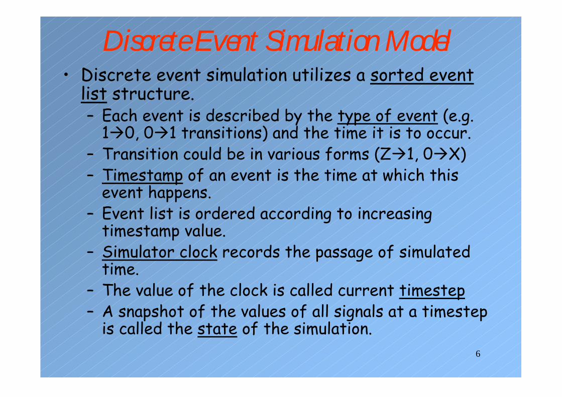
Discrete Event Simulation Model• Discrete event simulation utilizes a sorted event
list structure.– Each event is described by the type of event (e.g.
1�0, 0�1 transitions) and the time it is to occur.– Transition could be in various forms (Z�1, 0�X)– Timestamp of an event is the time at which this
event happens.– Event list is ordered according to increasing
timestamp value.– Simulator clock records the passage of simulated
time.– The value of the clock is called current timestep – A snapshot of the values of all signals at a timestep
is called the state of the simulation.

7
Discrete Event Simulation: Example 1• Half Adder
a
b
sum
carry
b
a
carry
sum
event
5 ns 10 15 20 25 30
8
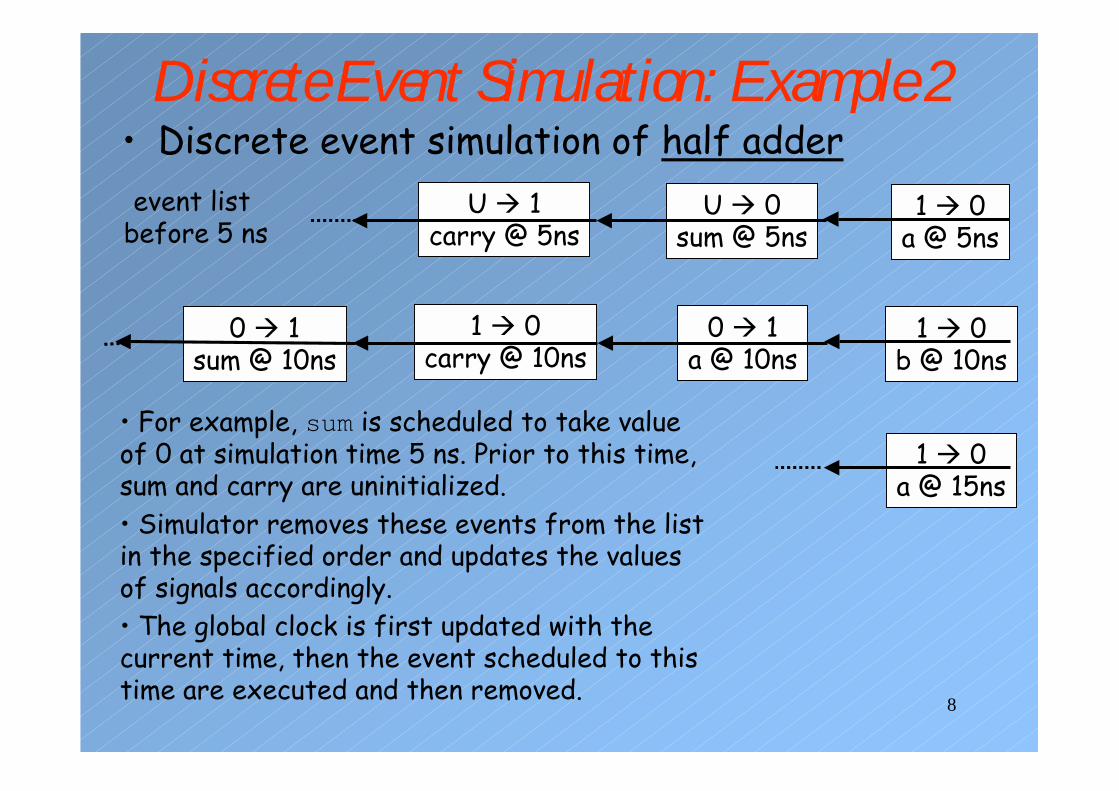
Discrete Event Simulation: Example 2• Discrete event simulation of half adder
1 � 0a @ 5ns
U � 0sum @ 5ns
U � 1carry @ 5ns
1 � 0b @ 10ns
0 � 1a @ 10ns
1 � 0carry @ 10ns
0 � 1sum @ 10ns
1 � 0a @ 15ns
• For example, sum is scheduled to take value of 0 at simulation time 5 ns. Prior to this time, sum and carry are uninitialized.• Simulator removes these events from the list in the specified order and updates the values of signals accordingly.• The global clock is first updated with the current time, then the event scheduled to this time are executed and then removed.
event list before 5 ns

9
Steps of the Simulation Model1. Advance the simulation time to that of the event with
the smallest timestamp in the event list. This is the event at the head of the sorted event list.
2. Execute all events at this timestep by updating signal values
3. All components affected by the new signal values must be re-evaluated( new events that may be generated as a result of changes in signal values must be scheduled by placing them in event list in the order of their timestamp)
4. Schedule future events5. Repeat until the event list is empty or preset
simulation time has expired.• The simulation model is very general such that it is
applicable to different levels of abstraction.

10
Logical Model vs. Physical Model• Discrete event simulation model is just an
approximation of behavior of real systems.– In fact, there are only analog devices where we
interpret analog voltage levels as logical 0 or 1.– We refer discrete event simulation model as logical
model while the real device as physical system– For better accuracy with which to capture the
behavior of physical system some complimentary techniques or models must be employed
– VHDL simulators provide facilities for setting the duration of a simulation timestep and query the contents of the event queue during simulation
– user can examine the event at the head of the event queue and force signals to specific values prior to next timestep.

11
Accuracy vs. Speed• Think of a 32-bit adder• Low accuracy:
– In VHDL, a 32-bit adder may be described in one line: two inputs and a single output. Inputs generate a value that appears at the output after some propagation delay.
– One step corresponds to the delay of adder– Easy, fast, and not too accurate
• High accuracy: – We might describe the adder at gate level– More realistic simulation– Has to handle many events– One step in the simulation corresponds to one gate
delay. – Naturally slow

12
Synthesis Model• Synthesis is a process
– Where a physical system is constructed from an abstract description using a pre-defined set of basic building blocks (e.g. logic gates, flip-flops, latches, small blocks of memory, LUTs in FPGA)
• Synthesis compilers operate on three types of information– Model of the circuit (e.g. VHDL model)– Set of constraints (speed, area, etc)– Set of components ( 2-input NAND gates, flip-flops
with asynchronous set and reset, etc.)

13
Design Process 1• We use
– Boolean expressions, truth tables, state diagrams to design a digital system.
– With synthesis tools, we can design digital systems at higher level of abstractions such as addition or multiplication of integers or real numbers, masking and shifting operations on Boolean strings, etc.
– The higher the level of abstraction you design at the less control over what is being synthesized by the compiler
– High-level synthesis problem is more challenging for the complier since it has to choose between alternatives
– The one chosen by the compiler may not be optimal.

14
Design Process 2• However,
– working at higher level of abstraction we will design the hardware in less time (shorter design cycle)
– It also facilitate design re-use and react to the future changes in the design
– For example, think of 32-bit adder– By specifying the design constraints the compiler
may choose between carry ripple adder (which is area optimized) and carry lookahead adder (which is time optimized)
15
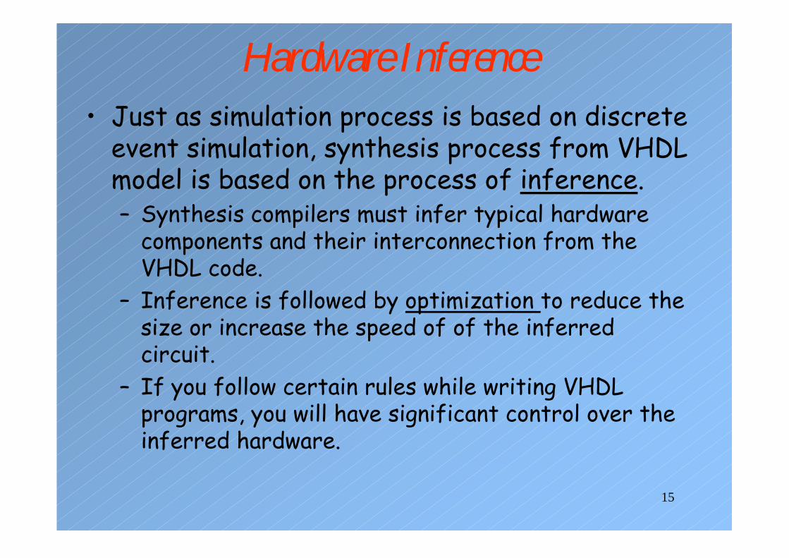
Hardware Inference• Just as simulation process is based on discrete
event simulation, synthesis process from VHDL model is based on the process of inference.– Synthesis compilers must infer typical hardware
components and their interconnection from the VHDL code.
– Inference is followed by optimization to reduce the size or increase the speed of of the inferred circuit.
– If you follow certain rules while writing VHDL programs, you will have significant control over the inferred hardware.

16
Hardware Inference: Example Inferring Combinational Logic
--
-- pseudo code for a single-bit arithmetic/logic unit
--
s1 <= in1 and in2;
s2 <= in1 or in2;
s3 <= in1 xor in2 xor c_in; -- perform the sum operation
c_out <= (in1 and c_in) or (in1 and in2) or (in1 and c_in);
z <= s1 when sel = “00” else
s2 when sel = “01” else
s3 when sel = “10” else‘0’;

17
Inferring Combinational Logic• Single-bit ALU
sel(1)sel(0)
in1in2
c_in
c_out
z
(in1·in2) sel(1)’·sel(0)’
(in1⊕ in2⊕ c_in) sel(1)·sel(0)’

18
Inferring Sequential Logic---- a simple conditional code block--
if (sel = ‘0’) then
z <= in1 nor in2;
end if;
sel
in1in2
z
• Inference of sequential components is more subtle.• Whether a latch of flip-flop is inferred depends on
the way we write your VHDL codes.• By careful coding, we can avoid unnecessary sequential
components (stay away from conventional programming techniques; stick to “hardware aware” approach)

19
Target Primitives 1• Target primitives are the building blocks
synthesis compiler use.– Example: Boolean equation, z = a’bc + b’c + db
z
abcbcdb
z
abcbcdb
c
b
c
d
a
z
• Simple fact: Circuit produced by the synthesis compiler depends on the set of available building blocks
20
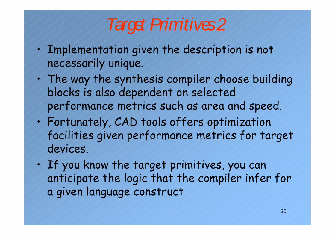
Target Primitives 2• Implementation given the description is not
necessarily unique.• The way the synthesis compiler choose building
blocks is also dependent on selected performance metrics such as area and speed.
• Fortunately, CAD tools offers optimization facilities given performance metrics for target devices.
• If you know the target primitives, you can anticipate the logic that the compiler infer for a given language construct

21
Field Programmable Gate Arrays (FPGA)• Reprogrammable hardware devices
– (Re)configurable hardware, reprogrammable hardware, etc.
– We are interested in one kind of such reprogrammable hardware: FPGA.
• Why Reprogrammable hardware?– ASIC offers the highest performance– But performs only one function– Development cost cannot be spread across multiple
applications– Ideal solution: change the interconnection between
millions of transistors comprising the chip in order to compute another function.

22
Basics of FPGA• Think of a cell (or block)
– That can be programmed to implement any small combinational or sequential circuit
– Tile the surface of a silicon die with these cells.– Wires running vertically and horizontally between these cells.
CLB CLB CLB
CLB CLB CLB
CLB CLB CLB
Any block can connect itself to horizontal or vertical wires that are adjacent to it.
Interconnect of the wires are called switching matrix.

23
Design with FPGA• Two types of blocks
– CLB – configurable logic blocks (inside the chip)– IOB - I/O blocks on the periphery (to drive the
signals off the chip and read the incoming signals)• Design process
1. Partition the “big” design into small sub-circuits.2. Each sub-circuit can be implemented in a CLB3. Establish the connections between sub-circuits
through the switching matrix4. If another design to be implemented, go to Step 1.

24
Inside the XC 4000 CLB• Many FPGAs look similar
– But they differ in how CLBs are implemented.– CLB is actually Xilinx terminology
• Main components in XC 4000 CLB – Two 16x1 RAM blocks – One 8x1 RAM block
• RAM can be used as LUT to implement combinational logic through truth tables
– Two edge-triggered D flip-flops• Can also be configured as latches
– Several multiplexors to configure the interconnection within the CLB.

25
Xilinx XC 4000 CLB
G4
G3
G2
G1
F4
F3
F2
F1
LogicFunction
of G1 – G4
LogicFunction
of F’, G’, H1
Logic
Function
of
F1 – F4
G
F
DIN
F ’G ’
H ’
DIN
F ’G ’
H ’
H H ’
G ’
K (clock)
EC
D QSD
RD1
S/R Control
S/R Control
EC
D QSD
RD1
H1DIN / H2 SR /
H0
EC
H ’
F ’X
Y
XQ
YQ
4
C1 … C4
bypass

26
Lookup Tables (LUT)• Combinational circuits are implemented using LUT
z
ab
cd
01111001110101100011111011010111001000011111010110110100001011100101001100000000zdcba

27
Combinational functions in LUT• Four inputs serve as the 4-bit address to the 16x1
memory• Single bit memory hold the output value corresponding
to the input value that is used as an address to access to this memory cell.
• 16x1 LUT can implement any Boolean function of four variables
• LUT is also referred as function generator.• Each CLB has two 4-bit function generators: F and G• The third generator, H, can implement any Boolean
function of three variables.– Two inputs come from the outputs of F and G.– The other input comes from outside

28
LUT • Using three function generators F, G, and H
– A single CLB can implement any Boolean function of five variables and some functions of up to nine variables
– It has nine logic inputs: F1, F2, F3, F4, G1, G2, G3, G4, and H1.
– General form of Boolean function of five variables:H = F(F1, F2, F3, F4)·H1’+ G(F1, F2, F3, F4 )·H1
• In some 4000 CLBs, LUTs can be configured as memory block– One 32x1 module– Dual ported 16x1 memory module– Synchronous-edge-triggered and asynchronous-
memory interfaces are supported
29
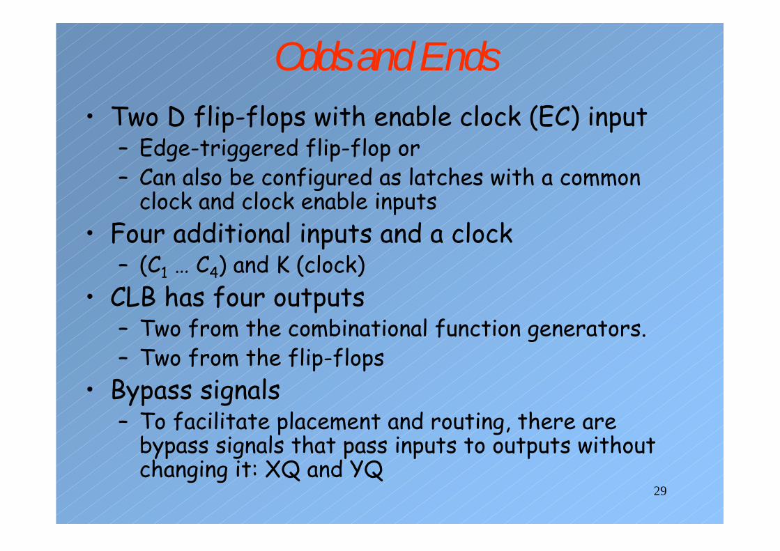
Odds and Ends• Two D flip-flops with enable clock (EC) input
– Edge-triggered flip-flop or– Can also be configured as latches with a common
clock and clock enable inputs• Four additional inputs and a clock
– (C1 … C4) and K (clock)• CLB has four outputs
– Two from the combinational function generators.– Two from the flip-flops
• Bypass signals– To facilitate placement and routing, there are
bypass signals that pass inputs to outputs without changing it: XQ and YQ

30
Odds and Ends• Many vendors typically supply implementation
of common building blocks that are optimized to the structure of their hardware components.– Xilinx, in fact, has a core generator utility that can
create common building blocks from parameterized descriptions provided by the user
– Adders, subtractors, multipliers, memories, etc. are such building blocks
• FPGA as a sea of LUTs and flip-flops– A gate-level design can be placed on the array by
mapping combinational components to function generators, sequential to flip-flops

31
Carry Logic 1• Each cell contains carry logic
for two bits
G
F
H
GCarry
FCarry
M3
M4
M2
M1
CIN UP
CIN DOWNCOUT
COUT
G4G3G2
G1
F3F2
F1
F4
32
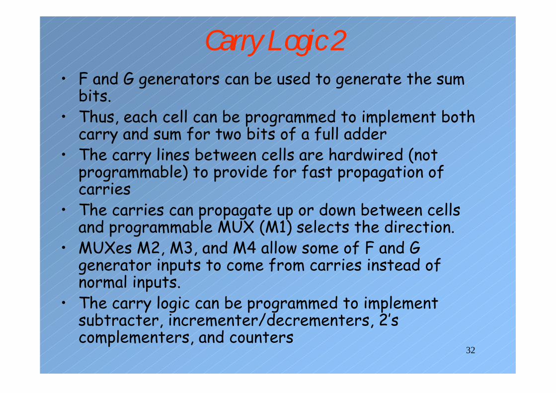
Carry Logic 2• F and G generators can be used to generate the sum
bits.• Thus, each cell can be programmed to implement both
carry and sum for two bits of a full adder• The carry lines between cells are hardwired (not
programmable) to provide for fast propagation of carries
• The carries can propagate up or down between cells and programmable MUX (M1) selects the direction.
• MUXes M2, M3, and M4 allow some of F and G generator inputs to come from carries instead of normal inputs.
• The carry logic can be programmed to implement subtracter, incrementer/decrementers, 2’s complementers, and counters

33
A CLB as Two-Bit Full Adder
G4: Ai+1
G1: Bi+1
F2: AiF1: Bi
Ci
G Function
F Function
Carry Logic
Si+1
Si
Ci+2
Ci+1
hardwired
hardwired

34
Connections for 4-bit Adder
CLB
CLB
CLB
CLBA1B1A0B0
C0
C0
C2
C3A3B3A2B2
C4
V
Hard-wired
• If we want to detect a possible overflow, we add the 4th CLB.
• The 3rd CLB outputs C3instead of C4 (How?)
• In the 4th CLB, C4 can be re-computed using the carry logic.
• Overflow is computed using the G function generator in the 4th CLB
• Overflow: V = C3⊕ C4• 4-bit adders can easily be
expanded 8 or 16-bit adders
• Adder modules are available in Xilinx library

35
F and G as RAM Memory: 16x2
G
F
G4
G3
G2
G1
F4
F3
F2
F1
WE DATAIN
WE DATAIN
MWRITE G
MWRITE F
WE D1 D0 EC
C1 C2 C3 C4
M16x2
Fi = Gi
C1 is write enable (WE)C2 and C3 are data inputs
Can it be configured as 32x1 memory?

36
IOB 1
CE
DQ
CE
D QOut
01
TS
Slew Ratecontrol
Passive Pull-UpPull-Down
OutputBuffer
InputBuffer
delay delay
G
DQ
Outputclock
pad
I1
I2
Clock enable
Inputclock
Fast Capture Latch
Output MUX
37
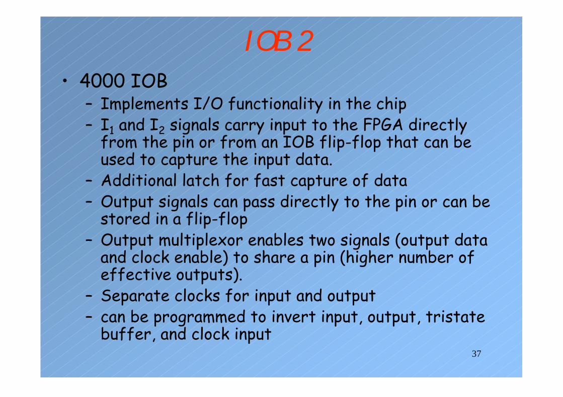
IOB 2• 4000 IOB
– Implements I/O functionality in the chip– I1 and I2 signals carry input to the FPGA directly
from the pin or from an IOB flip-flop that can be used to capture the input data.
– Additional latch for fast capture of data– Output signals can pass directly to the pin or can be
stored in a flip-flop– Output multiplexor enables two signals (output data
and clock enable) to share a pin (higher number of effective outputs).
– Separate clocks for input and output– can be programmed to invert input, output, tristate
buffer, and clock input

38
Switch Matrix• Different levels of interconnections
– Direct interconnects between CLBs. Short wires to connect adjacent CLBs in both directions.
– Switch matrix
CLB CLB CLB
CLB CLB CLB
CLB CLB CLB
PSM PSM
PSM PSM
• PSM: Programmable Switch Matrix
• PSM can be configured to connect a horizontal wire to a vertical one.
• One wire can be connected to multiple wires
• This way output of a CLB can routed through multiple PSMs to the input of another CLB.

39
PSM
CLB
12 4 42
2
12
6 4 8 4
8
4
3
3
Quad
Single
Double
long
Directconnect
long
long long DoubleQuad Directconnect
Carrychain
Single Globalclock
Globalclock

40
Types of Lines • Single-length: connects adjacent PSMs• Double-length: connects every other PSM• Quad-length: traverse four CLBs before passing
through a PSM.• Long: runs entire chip.
– Using tri-state buffers within the CBLSs, long lines can be configured as buses.
• Local connections use direct interconnect or single length lines in order to avoid to many switching points
• Global Nets: Low skew signal paths used to distribute high fan-out signals such as clock and reset signals.

41
Double Length Lines
CLB
CLB CLB
CLB CLB CLB
CLB CLB CLB
PSM PSM
PSM PSM

42
Example Interconnects
Direct interconnects between adjacent CLBs
CLB CLB CLB
CLB CLB CLB
CLB CLB CLB
PSM PSM
PSM PSM
PSM PSM
CLB
CLB CLB
CLB
General-purpose interconnects

43
Tri-state Buffers• Bus
– Each CLB has tri-state buffers that connect to long lines.
– Bus contention must be avoided
DAA
DBB
DCC
DNN
Z = DA A’ +DB B’ + DC C’ + … +DN N’
• Wired-AND implementation
DA
Z = DA DB DC … DN
DB DC DN
VCCVCC

44
Configuration 1• Configuration data for CLBs
– Provide the contents of the LUTs (16+16+8 = 40 bits)
– Configure multiplexors within the CLB– To determine the input sources of the flip-
flops, and the inputs to the H function etc.– Bits for configuring flip-flops
• Configuration data for PSM– Connecting horizontal and vertical lines– Tristate devices within the CLBs

45
Configuration 2
G4
G2
G1
F4
F3
F2
F1
LogicFunction
of G1 – G4
LogicFunction
of F’, G’, H1
Logic
Function
of
F1 – F4
G
F
DIN
F ’G ’
H ’
DIN
F ’G ’
H ’
H H ’
G ’
K (clock)
EC
D QSD
RD1
S/R Control
S/R Control
EC
D QSD
RD1
H1 DIN / H2 SR / H0
EC
H ’
F ’X
Y
XQ
YQ
4
C1 … C4
bypass
Xilinx X4000
M
M
46
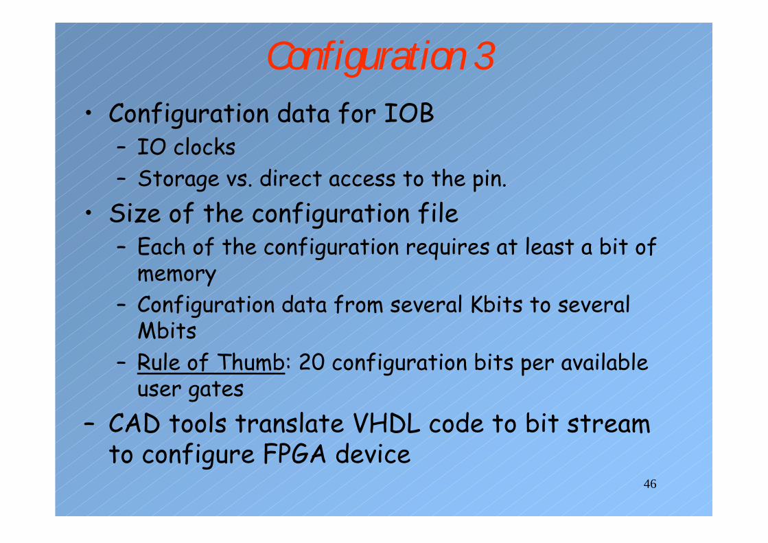
Configuration 3• Configuration data for IOB
– IO clocks– Storage vs. direct access to the pin.
• Size of the configuration file– Each of the configuration requires at least a bit of
memory– Configuration data from several Kbits to several
Mbits– Rule of Thumb: 20 configuration bits per available
user gates– CAD tools translate VHDL code to bit stream
to configure FPGA device

47
Configuration 4
Outputclock
Clock enable
Inputclock
CE
DQ
CE
D QOut
01
TS
Slew Ratecontrol
Passive Pull-UpPull-Down
OutputBuffer
InputBuffer
delay delay
G
DQ
pad
I1
I2
Fast Capture Latch
Output MUX
M
M
48
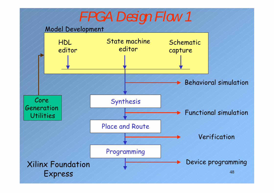
FPGA Design Flow 1
HDL editor
State machine editor
Schematic capture
Synthesis
Place and Route
Programming
Behavioral simulation
Functional simulation
Verification
Device programmingXilinx Foundation Express
Core Generation
Utilities
Model Development

49
FPGA Design Flow 2• Model development:
– VHDL code– State-machines may be described in a graphical manner and
translated into VHDL code.– Traditional schematic capture can be translated into VHDL
source.• Behavioral Simulation
– Before synthesis; for testing functional correctness• Synthesis
– The design is synthesized to a library of primitive components such as gates, flip-flops, and latches
• Functional Simulation– To find out preliminary performance estimates– For example, timing information can be obtained from known
properties of FPGA components– Still not too accurate

50
FPGA Design Flow 3• Place and Route:
– The design in mapped to the primitives in the target chip
– In FPGA, there are function generators, flip-flops, and latches
– Each primitive must be assigned to a specific CLB (Placement)
– Connections between CLBs that implement the primitives must be established (routing)
– Accurate timing can be obtained in Verification step(Post-placement and routing simulation)
– The configuration bits are generated.

51
FPGA Design Flow 4• Programming:
– The configuration data (bit stream) is finally loaded into the target FPGA chip.
• These steps are fairly generic although the terminology used here is adopted from Xilinx.

52
Xilinx Foundation Tools: Design Flow

53
Efficient Design
• Generally, we try to reduce the number of flip-flops in the design– X4000 (like many other FPGAs) has two flip-flops in
a CLB– Instead of trying to reduce the number of flip-
flops, try to reduce the number of CLBs and interconnects between them
• One-Hot State Assignment– Use one flip-flop for each state (N state N flip-
flops)

54
One-Hot State Assignment: Example• Four states: T0, T1, T2, and T3.• Four flip-flops: Q0, Q1, Q2, and Q3.• Assignment:• T0: (1000), T1: (0100), T2: (0010), T3: (0001).
T0 T1 T2
T3
X1/Z1
X2/Z2
X3/Z1
X4/Z2
Q3+ = X1Q0Q1’Q2’Q3’ +
X2Q0’Q1Q2’Q3’ +X3Q0’Q1’Q2Q3’ +X4Q0’Q1’Q2’Q3
= X1Q0 + X2Q1 +X3Q2 + X4Q3
Z1 = X1Q0 + X3Q2
Z2 = X2Q1 + X4Q3

55
One-Hot State Assignment: Example• With One-Hot state assignment, the next state
and output equations will contain one term for each arc leading into the corresponding state.
• Resetting the system requires one flip-flop be set to 1 instead of resetting all flip-flops to 0.– If flip-flops do not have a preset input (as in the case
for the Xilinx 3000 series).– New assignment:
T0: (0000), T1: (1100), T2: (1010), T3: (1001).
– Q3+ = X1Q0’ + X2Q1 +X3Q2 + X4Q3
– Z1 = X1Q0’ + X3Q2 and Z2 = X2Q1 + X4Q3

56
Typical FGPA • XC4003 FPGA
– Aprox. 3000 gates– 100 CLBs (10 x 10)– 80 user I/Os– 360 flip-flops (200 in CLBs and 160 in the IOB)– 45536 configuration bits
• XC4010E/XL– 7000 – 20000 Gates– 400 CLBs ( 20 x 20)– 160 User I/O– 1120 flip-flops– Several hundred bits of configuration data per CLB

57
Summary• Simulation Model
– Discrete event execution model for VHDL programs– Accuracy vs. time
• Synthesis Model– Need for inference from language constructs– Basic principles behind the use of FPGAs– Challenges in the design flow