simultaneous coulomb blockade for electrons and holes in p–n junctions: observation of coulomb...
TRANSCRIPT
Physica E 8 (2000) 5–12www.elsevier.nl/locate/physe
Simultaneous Coulomb blockade for electrons and holes in p–njunctions: observation of Coulomb staircase and turnstile operation
Oliver Bensona;b; ∗, Jungsang Kima, Hirofumi Kanc, Yoshihisa Yamamotoa;d
aERATO Quantum Fluctuation Project, E. L. Ginzton Laboratory, Stanford University, Stanford, CA 94305, USAbSektion Naturwissenschaften, Fachbereich Physik, Universit�at Konstanz, Universit�atsstr. 10, 78464 Konstanz, Germany
cCentral Research Laboratory, Hamamatsu Photonics Inc., Hamamatsu, Shizuoka, JapandNTT Basic Research Laboratories, 3-1 Morinosato-Wakamiya Atsugi, Kanagawa, 243-01, Japan
Received 27 October 1999; received in revised form 7 January 2000; accepted 1 February 2000
Abstract
The Coulomb blockade e�ect in a mesoscopic double-barrier p–i–n junction is reported. The electron and hole injection intothe central QW of a p–n junction is achieved via resonant tunneling. We present a theoretical model that describes the deviceoperation. When the device is biased with a constant voltage source the model predicts the observation of Coulomb staircasein the current–voltage characteristics. When an additional square wave modulation signal is applied, turnstile operation isachieved. The experimental evidence for Coulomb staircase e�ect and turnstile operation is presented. ? 2000 ElsevierScience B.V. All rights reserved.
PACS: 73.23.Hk; 73.40.Kp; 73.20.Dx
Keywords: Coulomb blockade; Mesoscopic physics; Nanostructures; p–n junction; Resonant tunneling
1. Introduction
Coulomb blockade e�ect in a mesoscopic tunneljunction, where the single electron charging energyis larger than the thermal energy and so the tunnel-ing of electrons is mutually correlated [1], has beena �eld of intense research for last few years since
∗ Correspondence address: Sektion Naturwissenschaften, Fach-bereich Physik, Universit�at Konstanz, Universit�atsstr. 10, 78464Konstanz, Germany. Tel.: +49-7531-88-3824; fax: +49-7531-88-3072.E-mail address: [email protected] (O. Benson).
the �rst theoretical prediction [2,3] and experimentaldemonstration [4,5]. Time correlation as a result ofCoulomb interaction between electrons leads to non-linearities in the current–voltage (I–V ) characteristicsin double tunnel junctions, known as Coulomb stair-case [6]. A single electron transistor [3], where thecurrent through the device is determined by the charg-ing state of the central island that is controlled bymeans of a third gate electrode, proves to be a practi-cal device to be used as an electrometer [7,8]. Semi-conductor single electron transistors where electronscan be added to the central island one by one start-ing from an empty island were demonstrated [9–11].
1386-9477/00/$ - see front matter ? 2000 Elsevier Science B.V. All rights reserved.PII: S 1386 -9477(00)00123 -5

6 O. Benson et al. / Physica E 8 (2000) 5–12
Coulomb and exchange interactions between electronsas well as angular momentum shell structures can bestudied in such a device. Single electron turnstilesand pumps where electron transport can be regulatedone by one with an AC modulation signal, have beendemonstrated both in multiple M–I–M tunnel junc-tions [12,13] and in semiconductor quantum dots ina two-dimensional electron gas system [14], and areexpected to be used as a current standard. Multipleelectronic islands have been coupled by Coulomb in-teraction or electron tunneling. At low temperaturesthe interplay between quantum and electrostatic e�ectsdetermines the properties of these systems [15–17].Transport properties and the formation of “arti�cialmolecule” [18] states have attracted broad interest.Most of the devices studied above are unipolar,
i.e., they utilize the Coulomb blockade e�ect on a sin-gle type of carrier. Simultaneous Coulomb blockadee�ect for electrons and holes in a mesoscopic p–njunction was studied by Imamo�glu and Yamamoto[19,20], and it was demonstrated that nonclassicallight can be generated from such a structure. A singlephoton turnstile device, where a single electron and asingle hole is injected into the optically active regionof a p–n junction to generate a stream of regulatedsingle photons, was proposed [21] and demonstrated[22]. In such a p–n junction structure, electron and holeinjection is split into two di�erent bands (conductionand valence band) across an energy gap. It is possiblethat the electron and hole tunneling conditions areseparated in applied bias voltage, and thus can becontrolled independently. In this paper, we reportan experimental evidence of simultaneous Coulombblockade e�ect for electrons and holes in a p–n junc-tion. In DC operation, when the device is drivenby a constant voltage source, Coulomb staircase isobserved. In AC operation, when a square wave mod-ulation signal is applied, a characteristic frequencydependence of the average current gives experimen-tal evidence for turnstile operation. We present aphysical model along with Monte-Carlo simulationresults, that explains the device operation for thesetwo operation regimes.
2. Principle of operation
Fig. 1(a) shows the schematic band diagram ofthe device considered in this paper. It consists of
Fig. 1. (a) Schematic energy-band diagram of the p–i–n junctionand (b) sketch of the micropost structure (not to scale).
an intrinsic central 10 nm GaAs QW isolated by20 nm Al0:18Ga0:82As barriers from 9 and 7.5 nmAl0:12Ga0:88As QWs on the n- and p-side, respec-tively. The side QWs are not deliberately doped,but carriers are supplied from nearby n-type lead(2× 1017 cm−3) and p-type lead (5× 1018 cm−3)by modulation doping. We also fabricated a devicewith a 20% smaller barrier width on both the n- andp-side. In the following, we will denote the two typesof devices as low-tunneling rate and high-tunnelingrate device. The lateral size of the device is reducedto increase the single charging energy e2=C, whereC = Cn + Cp is the total capacitance, i.e., the sum ofthe capacitance between the central-quantum well andthe n- and p-side, respectively. This is accomplishedby de�ning small devices using e-beam lithography(device diameter =600 nm) and fabricating poststructures by electron–cyclotron resonance reactiveion etching (ECR-RIE) in Cl2=BCl3 plasma. Thesurface of the device was passivated with sulfur inammonium sul�de solution in order to reduce surfaceleakage current. After planarization with hard-bakedphotoresist, electrical p-type contacts were made on
O. Benson et al. / Physica E 8 (2000) 5–12 7
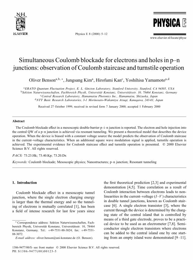
Fig. 2. Principle of DC device operation. The rising edges ofelectron and hole tunneling rates versus bias voltage are plotted.The numbers of electrons in the central QW are ne − 1 (dashed),ne (solid), and ne + 1 (dotted).
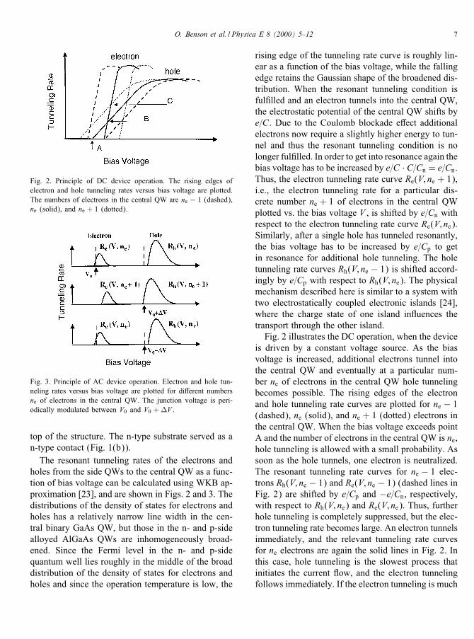
Fig. 3. Principle of AC device operation. Electron and hole tun-neling rates versus bias voltage are plotted for di�erent numbersne of electrons in the central QW. The junction voltage is peri-odically modulated between V0 and V0 + �V .
top of the structure. The n-type substrate served as an-type contact (Fig. 1(b)).The resonant tunneling rates of the electrons and
holes from the side QWs to the central QW as a func-tion of bias voltage can be calculated using WKB ap-proximation [23], and are shown in Figs. 2 and 3. Thedistributions of the density of states for electrons andholes has a relatively narrow line width in the cen-tral binary GaAs QW, but those in the n- and p-sidealloyed AlGaAs QWs are inhomogeneously broad-ened. Since the Fermi level in the n- and p-sidequantum well lies roughly in the middle of the broaddistribution of the density of states for electrons andholes and since the operation temperature is low, the
rising edge of the tunneling rate curve is roughly lin-ear as a function of the bias voltage, while the fallingedge retains the Gaussian shape of the broadened dis-tribution. When the resonant tunneling condition isful�lled and an electron tunnels into the central QW,the electrostatic potential of the central QW shifts bye=C. Due to the Coulomb blockade e�ect additionalelectrons now require a slightly higher energy to tun-nel and thus the resonant tunneling condition is nolonger ful�lled. In order to get into resonance again thebias voltage has to be increased by e=C · C=Cn = e=Cn.Thus, the electron tunneling rate curve Re(V; ne + 1),i.e., the electron tunneling rate for a particular dis-crete number ne + 1 of electrons in the central QWplotted vs. the bias voltage V , is shifted by e=Cn withrespect to the electron tunneling rate curve Re(V; ne).Similarly, after a single hole has tunneled resonantly,the bias voltage has to be increased by e=Cp to getin resonance for additional hole tunneling. The holetunneling rate curves Rh(V; ne − 1) is shifted accord-ingly by e=Cp with respect to Rh(V; ne). The physicalmechanism described here is similar to a system withtwo electrostatically coupled electronic islands [24],where the charge state of one island in uences thetransport through the other island.Fig. 2 illustrates the DC operation, when the device
is driven by a constant voltage source. As the biasvoltage is increased, additional electrons tunnel intothe central QW and eventually at a particular num-ber ne of electrons in the central QW hole tunnelingbecomes possible. The rising edges of the electronand hole tunneling rate curves are plotted for ne − 1(dashed), ne (solid), and ne + 1 (dotted) electrons inthe central QW. When the bias voltage exceeds pointA and the number of electrons in the central QW is ne,hole tunneling is allowed with a small probability. Assoon as the hole tunnels, one electron is neutralized.The resonant tunneling rate curves for ne − 1 elec-trons Rh(V; ne − 1) and Re(V; ne − 1) (dashed lines inFig. 2) are shifted by e=Cp and −e=Cn, respectively,with respect to Rh(V; ne) and Re(V; ne). Thus, furtherhole tunneling is completely suppressed, but the elec-tron tunneling rate becomes large. An electron tunnelsimmediately, and the relevant tunneling rate curvesfor ne electrons are again the solid lines in Fig. 2. Inthis case, hole tunneling is the slowest process thatinitiates the current ow, and the electron tunnelingfollows immediately. If the electron tunneling is much
8 O. Benson et al. / Physica E 8 (2000) 5–12
larger than the hole tunneling, the current is propor-tional to the hole tunneling rate and features a linearincrease with increasing bias voltage. The slope of thelinear increase is determined by the hole tunneling ratecurve.As the bias voltage is increased above point B, both
electron and hole can tunnel, but the electron tunnel-ing rate is larger than the hole tunneling rate. Occa-sionally, a hole tunneling occurs �rst, in which casethe current ows by the same mechanism as betweenpoints A and B discussed above. But, most of the timean electron tunnels �rst, and the tunneling rate curvesfor ne + 1 electrons Rh(V; ne + 1) and Re(V; ne + 1)(dotted lines in Fig. 2) are shifted by −e=Cp and e=Cn,respectively, with respect to Rh(V; ne) and Re(V; ne).Further electron tunneling is suppressed, and hole tun-neling becomes larger. A hole tunneling will follow,and the relevant tunneling rate curves for ne electronsare again the solid lines in Fig. 2. Since the electrontunneling rate (for the solid line) is smaller than thehole tunneling rate (for the dotted line) between pointsB and C, the electron tunneling “triggers” the current ow in this case, and the hole tunneling immediatelyfollows. The current features a steep linear increase,determined by the electron tunneling rate curve.When the bias voltage is increased above point C,
again the device is mostly waiting for the hole to tun-nel, and the current features the slower linear increaseof the hole tunneling rate curve. This shows that aCoulomb staircase is observed in the DC I–V char-acteristics, which re ects the charging of the centralQW by discrete steps of e and the asymmetry (dif-ferent slopes) between the electron and hole resonanttunneling rate curves. If the slope of the electron tun-neling rate curve is much larger than the slope of thehole tunneling rate curve, the Coulomb staircase stepsoccur whenever the bias voltage is increased by anadditional e=Cp.Fig. 3 illustrates the AC operation when a square
wave modulation signal of amplitude �V and fre-quency f = 1=T is added to a �xed bias voltage V0.In the �rsthalf of the modulation cycle at V0 onlyelectrons can tunnel into the central QW (Fig. 3 top).If one electron tunnels the electron and hole tunnel-ing rate curves for succeeding electrons and holes,Re(V; ne + 1) and Rh(V; ne + 1), are shifted by e=Cnand −e=Cp, respectively, with respect to Re(V; ne)and Rh(V; ne) due to single electron charging energy
(Fig. 3 middle). In the second half of the modulationcycle at V0 + �V only hole tunneling is possible. Ifa hole tunnels one electron is neutralized the originalstate is recovered (Fig. 3 bottom).If the probability for electron (hole) tunneling
within T=2 at V0 (V0 + �V ) is large, each electron(hole) tunneling event shifts the electron (hole) tun-neling rate curve Re(V; ne) (Rh(V; ne)) for succeed-ing electrons (holes) upwards towards Re(V; ne +1) (Rh(V; ne − 1)) until further electron (hole) tun-neling is completely suppressed. A constant numbern(V0;�V ) of electrons and holes tunnels within eachmodulation cycle. The current at the bias voltage V0is proportional to the modulation frequency:
I(V0;�V ) = n(V0;�V )e=T = n(V0;�V )ef: (1)
This case is the turnstile operation. At a low DC biasvoltage one hole tunneling event is su�cient to sup-press further hole tunneling (Fig. 3) and n(V0;�V ) =1. If the bias voltage V0 is increased two electrons andtwo holes can tunnel within T=2. In general, increas-ing V0 increases the number of holes and electronsthat tunnel into the central QW per modulation periodone by one. Thus, the I–V curve displays plateaus atinteger multiples of ef.If the modulation frequency becomes comparable
to the electron or hole tunneling rate at V0 and V0 +�V , respectively, not enough electrons or holes tunnelwithin T=2 to supress further electron (hole) tunnelingcompletely. The number of electrons and holes thattunnel within T=2 is no longer �xed and the plateausin the I–V curve are averaged out. A sub-linear fre-quency dependence of the average current remains inthis case.
3. Monte-Carlo simulation
We performed Monte-Carlo numerical simulations[16] to con�rm our theoretical model and to illustratethe device operation in the DC and AC mode. Fur-thermore, a dependence on experimental parameters,such as the slope of the electron and hole tunnelingrate curve can be illustrated. In the simulations we as-sumed Cp = Cn = C=2 = 0:05f F. The tunneling ratecurves are approximated in the simulation by a linearrising edge and a Gaussian shaped falling edge.
O. Benson et al. / Physica E 8 (2000) 5–12 9
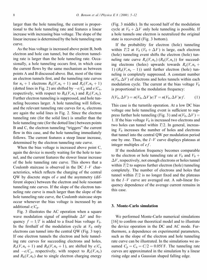
Fig. 4. Monte-Carlo simulation of I–V curves in DC operation. Thelinear slopes of the electron resonant tunneling curve is decreasedfrom in�nity (rightmost curve) to 32 MHz=(e=C) (leftmost curve).The slope of the linear rising edge of the hole tunneling rate curveis �xed at 26 MHz=(e=C).
Fig. 4 shows calculated I–V curves in DC operationas the slope of the linear rising edge of the electron tun-neling rate curve Re(V; ne) is varied. From right to leftthe slope is decreased from in�nity to 32 MHz=(e=C).The slope of the linear rising edge of the hole tunnel-ing rate curve is �xed at 26 MHz=(e=C). The maxi-mum tunneling rate for electrons and holes is 120 and240 MHz, respectively. In the rightmost curve pro-nounced Coulomb staircase steps are observed. Thecurve features the two di�erent linear slopes of theelectron and hole tunneling rate curves. As the slopeof the electron tunneling rate curve is decreased andapproaches the slope of the hole tunneling rate curvethe Coulomb staircase becomes less pronounced. Anadditional requirement to observe Coulomb staircaseis that the tunneling of a single electron (hole) mustchange the electron (hole) tunneling rate signi�cantly.After one electron has tunneled, the electron tunnnel-ing rate has to be reduced and the hole tunneling ratehas to be enhanced, so that the next most probableevent is hole tunneling, and vice versa. This maintainsthe subsequent electron–hole tunneling in DC opera-tion as described in the above section.Fig. 5 shows calculated I–V curves in AC operation,
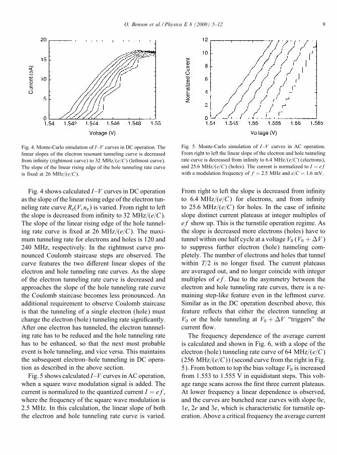
when a square wave modulation signal is added. Thecurrent is normalized to the quantized current I = ef,where the frequency of the square wave modulation is2.5 MHz. In this calculation, the linear slope of boththe electron and hole tunneling rate curve is varied.
Fig. 5. Monte-Carlo simulation of I–V curves in AC operation.From right to left the linear slope of the electron and hole tunnelingrate curve is decreased from in�nity to 6:4 MHz=(e=C) (electrons),and 25:6 MHz=(e=C) (holes). The current is normalized to I = efwith a modulation frequency of f = 2:5 MHz and e=C = 1:6 mV.
From right to left the slope is decreased from in�nityto 6:4 MHz=(e=C) for electrons, and from in�nityto 25:6 MHz=(e=C) for holes. In the case of in�niteslope distinct current plateaus at integer multiples ofef show up. This is the turnstile operation regime. Asthe slope is decreased more electrons (holes) have totunnel within one half cycle at a voltage V0 (V0 + �V )to suppress further electron (hole) tunneling com-pletely. The number of electrons and holes that tunnelwithin T=2 is no longer �xed. The current plateausare averaged out, and no longer coincide with integermultiples of ef. Due to the asymmetry between theelectron and hole tunneling rate curves, there is a re-maining step-like feature even in the leftmost curve.Similar as in the DC operation described above, thisfeature re ects that either the electron tunneling atV0 or the hole tunneling at V0 + �V “triggers” thecurrent ow.The frequency dependence of the average current
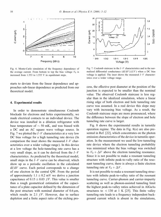
is calculated and shown in Fig. 6, with a slope of theelectron (hole) tunneling rate curve of 64 MHz=(e=C)(256 MHz=(e=C)) (second curve from the right in Fig.5). From bottom to top the bias voltage V0 is increasedfrom 1.553 to 1.555 V in equidistant steps. This volt-age range scans across the �rst three current plateaus.At lower frequency a linear dependence is observed,and the curves are bunched near curves with slope 0e,1e, 2e and 3e, which is characteristic for turnstile op-eration. Above a critical frequency the average current
10 O. Benson et al. / Physica E 8 (2000) 5–12
Fig. 6. Monte-Carlo simulation of the frequency dependence ofthe average current. From bottom to top the bias voltage V0 isincreased from 1.553 to 1:555 V in equidistant steps.
starts to deviate from the linear dependence and ap-proaches sub-linear dependence as predicted from ourtheoretical model.
4. Experimental results
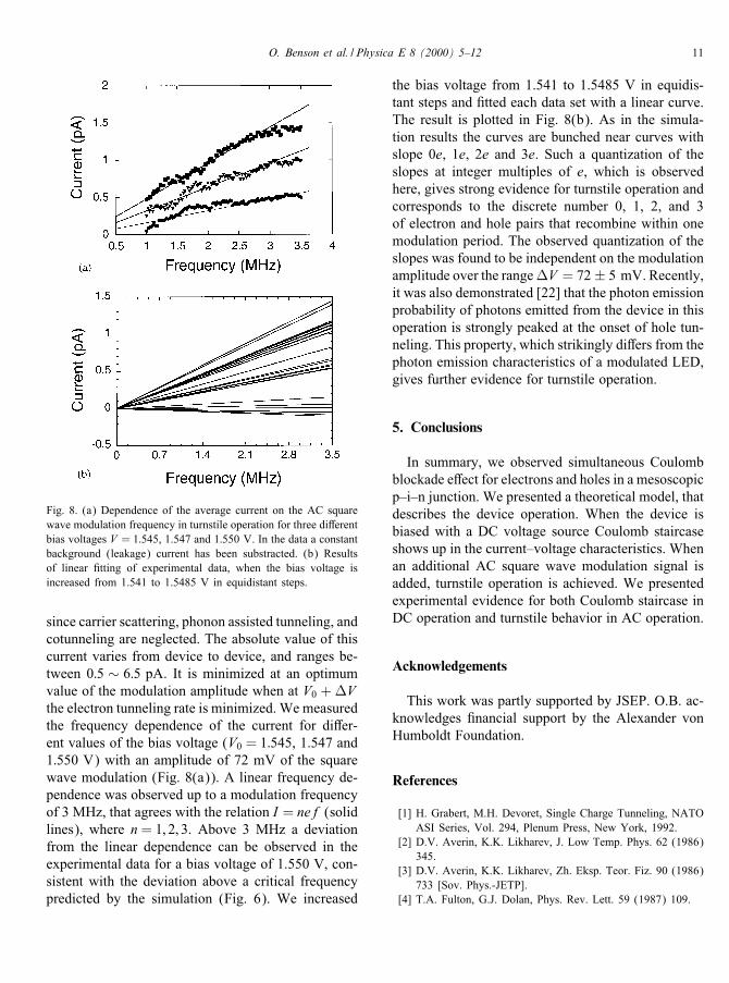
In order to demonstrate simultaneous Coulombblockade for electrons and holes experimentally, wemade electrical contacts to an individual device. Thedevice was installed in a dilution refrigerator withbase temperature of ∼ 50 mK, and was biased witha DC and an AC square wave voltage source. InFig. 7 we plotted the I–V characteristics at a very lowDC bias voltage for a high tunneling rate device (Incomparison the inset shows the measured I–V char-acteristics over a wider voltage range). In this deviceat a low voltage the hole-tunneling rate curve has avery small slope, as it can be derived from the I–Vcharacteristics. As predicted by the theoretical model,small steps in the I–V curve can be observed, whichshow up as a periodic oscillation in the calculateddI=dV curve. Each period corresponds to a changeof one electron in the central QW. From the periodof approximately 1:1± 0:2 mV we derive a junctioncapacitance of 0:15± 0:03 fF . This value is smallerthan a rough geometrical estimation of the capaci-tance of a plate capacitor de�ned by the dimension ofthe post structure with nominal diameter of 0:6�m,which results in 2:1 fF . However, due to surfacedepletion and a �nite aspect ratio of the etching pro-
Fig. 7. Coulomb staircase in the I–V characteristics and in the nor-malized di�erential conductance (dI=dV )=(I=V ) when a DC biasvoltage is applied. The inset shows the measured I–V character-istics over a wider voltage range.
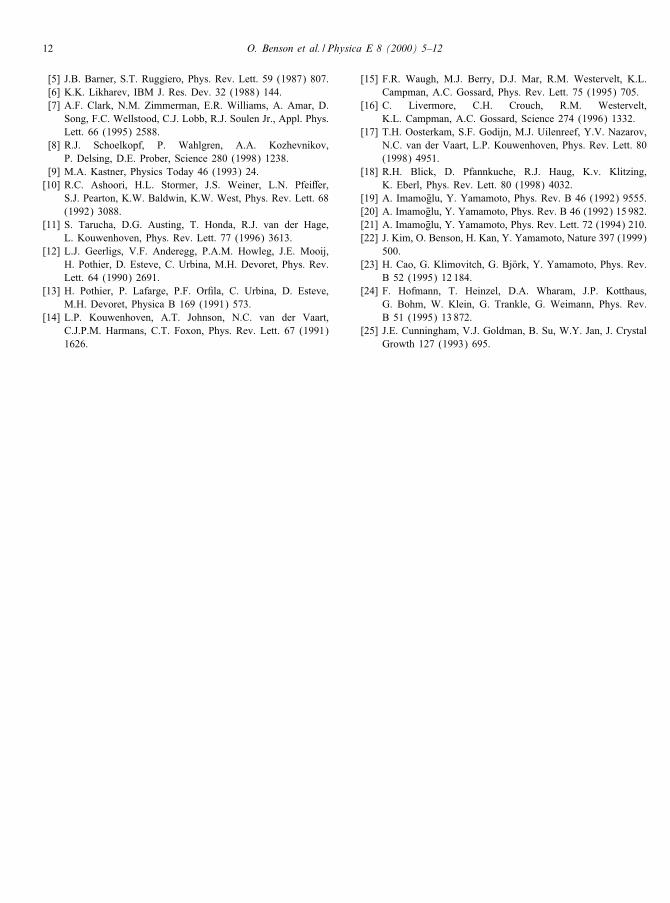
cess, the e�ective post diameter at the position of thejunction is expected to be smaller than the nominalvalue. The observed Coulomb staircase is less reg-ular than in the idealized simulation, where a linearrising edge of both electron and hole tunneling ratecurve was assumed. In a real device this slope mayvary with increasing bias voltage. As a result, theCoulomb staircase steps are more pronounced, wherethe di�erence between the slope of electron and holetunneling rate curve is larger.Fig. 8 shows the experimental results in turnstile
operation regime. The data in Fig. 8(a) are also pre-sented in Ref. [22], which concentrates on the photonemission characteristics of the device in turnstile oper-ation. In the measurement we used the low-tunnelingrate device where the electron tunneling probabilitywas minimized when the bias voltage was switchedto V0 + �V above the electron tunneling resonance.Since it is not possible to make a resonant tunnelingstructure with in�nite peak-to-vally ratio of the reso-nant tunneling curve, there is always a �nite electrontunneling rate at V0 + �V .It is not possible to make a resonant tunneling struc-
ture with in�nite peak-to-valley ratio of the resonanttunneling curve. Carrier-phonon and carrier-impurityscattering as well as phonon-assisted tunneling limitthe highest peak-to-valley ratios achieved in AlGaAsstructures to ¡ 130 at 1 K [25]. This �nite valleytunneling rate leads to a frequency independent back-ground current which is absent in the simulations,
O. Benson et al. / Physica E 8 (2000) 5–12 11
Fig. 8. (a) Dependence of the average current on the AC squarewave modulation frequency in turnstile operation for three di�erentbias voltages V = 1:545, 1.547 and 1:550 V. In the data a constantbackground (leakage) current has been substracted. (b) Resultsof linear �tting of experimental data, when the bias voltage isincreased from 1.541 to 1.5485 V in equidistant steps.
since carrier scattering, phonon assisted tunneling, andcotunneling are neglected. The absolute value of thiscurrent varies from device to device, and ranges be-tween 0:5 ∼ 6:5 pA. It is minimized at an optimumvalue of the modulation amplitude when at V0 + �Vthe electron tunneling rate is minimized. We measuredthe frequency dependence of the current for di�er-ent values of the bias voltage (V0 = 1:545, 1.547 and1:550 V) with an amplitude of 72 mV of the squarewave modulation (Fig. 8(a)). A linear frequency de-pendence was observed up to a modulation frequencyof 3 MHz, that agrees with the relation I = nef (solidlines), where n= 1; 2; 3. Above 3 MHz a deviationfrom the linear dependence can be observed in theexperimental data for a bias voltage of 1.550 V, con-sistent with the deviation above a critical frequencypredicted by the simulation (Fig. 6). We increased
the bias voltage from 1.541 to 1.5485 V in equidis-tant steps and �tted each data set with a linear curve.The result is plotted in Fig. 8(b). As in the simula-tion results the curves are bunched near curves withslope 0e, 1e, 2e and 3e. Such a quantization of theslopes at integer multiples of e, which is observedhere, gives strong evidence for turnstile operation andcorresponds to the discrete number 0, 1, 2, and 3of electron and hole pairs that recombine within onemodulation period. The observed quantization of theslopes was found to be independent on the modulationamplitude over the range�V = 72± 5 mV. Recently,it was also demonstrated [22] that the photon emissionprobability of photons emitted from the device in thisoperation is strongly peaked at the onset of hole tun-neling. This property, which strikingly di�ers from thephoton emission characteristics of a modulated LED,gives further evidence for turnstile operation.
5. Conclusions
In summary, we observed simultaneous Coulombblockade e�ect for electrons and holes in a mesoscopicp–i–n junction. We presented a theoretical model, thatdescribes the device operation. When the device isbiased with a DC voltage source Coulomb staircaseshows up in the current–voltage characteristics. Whenan additional AC square wave modulation signal isadded, turnstile operation is achieved. We presentedexperimental evidence for both Coulomb staircase inDC operation and turnstile behavior in AC operation.
Acknowledgements
This work was partly supported by JSEP. O.B. ac-knowledges �nancial support by the Alexander vonHumboldt Foundation.
References
[1] H. Grabert, M.H. Devoret, Single Charge Tunneling, NATOASI Series, Vol. 294, Plenum Press, New York, 1992.
[2] D.V. Averin, K.K. Likharev, J. Low Temp. Phys. 62 (1986)345.
[3] D.V. Averin, K.K. Likharev, Zh. Eksp. Teor. Fiz. 90 (1986)733 [Sov. Phys.-JETP].
[4] T.A. Fulton, G.J. Dolan, Phys. Rev. Lett. 59 (1987) 109.
12 O. Benson et al. / Physica E 8 (2000) 5–12
[5] J.B. Barner, S.T. Ruggiero, Phys. Rev. Lett. 59 (1987) 807.[6] K.K. Likharev, IBM J. Res. Dev. 32 (1988) 144.[7] A.F. Clark, N.M. Zimmerman, E.R. Williams, A. Amar, D.
Song, F.C. Wellstood, C.J. Lobb, R.J. Soulen Jr., Appl. Phys.Lett. 66 (1995) 2588.
[8] R.J. Schoelkopf, P. Wahlgren, A.A. Kozhevnikov,P. Delsing, D.E. Prober, Science 280 (1998) 1238.
[9] M.A. Kastner, Physics Today 46 (1993) 24.[10] R.C. Ashoori, H.L. Stormer, J.S. Weiner, L.N. Pfei�er,
S.J. Pearton, K.W. Baldwin, K.W. West, Phys. Rev. Lett. 68(1992) 3088.
[11] S. Tarucha, D.G. Austing, T. Honda, R.J. van der Hage,L. Kouwenhoven, Phys. Rev. Lett. 77 (1996) 3613.
[12] L.J. Geerligs, V.F. Anderegg, P.A.M. Howleg, J.E. Mooij,H. Pothier, D. Esteve, C. Urbina, M.H. Devoret, Phys. Rev.Lett. 64 (1990) 2691.
[13] H. Pothier, P. Lafarge, P.F. Or�la, C. Urbina, D. Esteve,M.H. Devoret, Physica B 169 (1991) 573.
[14] L.P. Kouwenhoven, A.T. Johnson, N.C. van der Vaart,C.J.P.M. Harmans, C.T. Foxon, Phys. Rev. Lett. 67 (1991)1626.
[15] F.R. Waugh, M.J. Berry, D.J. Mar, R.M. Westervelt, K.L.Campman, A.C. Gossard, Phys. Rev. Lett. 75 (1995) 705.
[16] C. Livermore, C.H. Crouch, R.M. Westervelt,K.L. Campman, A.C. Gossard, Science 274 (1996) 1332.
[17] T.H. Oosterkam, S.F. Godijn, M.J. Uilenreef, Y.V. Nazarov,N.C. van der Vaart, L.P. Kouwenhoven, Phys. Rev. Lett. 80(1998) 4951.
[18] R.H. Blick, D. Pfannkuche, R.J. Haug, K.v. Klitzing,K. Eberl, Phys. Rev. Lett. 80 (1998) 4032.
[19] A. Imamo�glu, Y. Yamamoto, Phys. Rev. B 46 (1992) 9555.[20] A. Imamo�glu, Y. Yamamoto, Phys. Rev. B 46 (1992) 15 982.[21] A. Imamo�glu, Y. Yamamoto, Phys. Rev. Lett. 72 (1994) 210.[22] J. Kim, O. Benson, H. Kan, Y. Yamamoto, Nature 397 (1999)
500.[23] H. Cao, G. Klimovitch, G. Bj�ork, Y. Yamamoto, Phys. Rev.
B 52 (1995) 12 184.[24] F. Hofmann, T. Heinzel, D.A. Wharam, J.P. Kotthaus,
G. Bohm, W. Klein, G. Trankle, G. Weimann, Phys. Rev.B 51 (1995) 13 872.
[25] J.E. Cunningham, V.J. Goldman, B. Su, W.Y. Jan, J. CrystalGrowth 127 (1993) 695.