simultaneous multi-mastering with the nios processor … · sopc builder views ... simultaneous...
TRANSCRIPT

Tutorial
Simultaneous Multi-Masteringwith the Nios Processor
101 Innovation DriveSan Jose, CA 95134(408) 544-7000 Document Version: 1.0.0 rev. 1http://www.altera.com Document Date: June 2002

ii Altera Corporation
Copyright Simultaneous Multi-Mastering with the Nios Processor Tutorial
Copyright © 2002 Altera Corporation. All rights reserved. Altera, The Programmable Solutions Company, the stylized Altera logo,specific device designations, and all other words and logos that are identified as trademarks and/or service marks are, unlessnoted otherwise, the trademarks and service marks of Altera Corporation in the U.S. and other countries. All other product orservice names are the property of their respective holders. Altera products are protected under numerous U.S. and foreign patentsand pending applications, mask work rights, and copyrights. Altera warrants performance of its semiconductorproducts to current specifications in accordance with Altera’s standard warranty, but reserves the right to makechanges to any products and services at any time without notice. Altera assumes no responsibility or liabilityarising out of the application or use of any information, product, or service described herein except as expresslyagreed to in writing by Altera Corporation. Altera customers are advised to obtain the latest version of devicespecifications before relying on any published information and before placing orders for products or services.
TU-NIOSSMM-1.0

Altera Corporation
About this Document
This tutorial introduces you to the simultaneous multi-mastering feature of the Altera® Nios® embedded processor. It shows you how to use the Quartus® II software to optimize a Nios design using this feature.
Table 1 shows the tutorial revision history.
f Refer to the Nios embedded processor readme file for late-breaking information that is not available in this user guide.
How to Find Information
■ The Adobe Acrobat Find feature allows you to search the contents of a PDF file. Click the binoculars toolbar icon to open the Find dialog box.
■ Bookmarks serve as an additional table of contents.■ Thumbnail icons, which provide miniature previews of each page,
provide a link to the pages.■ Numerous links, shown in green text, allow you to jump to related
information.
Table 1. Tutorial Revision History
Date Description
June 2002, v1.0 rev. 1
First release of tutorial.
iii

About this Document Simultaneous Multi-Mastering with the Nios Processor Tutorial
How to Contact Altera
For the most up-to-date information about Altera products, go to the Altera world-wide web site at http://www.altera.com.
For technical support on this product, go to http://www.altera.com/mysupport. For additional information about Altera products, consult the sources shown in Table 2.
Note:(1) You can also contact your local Altera sales office or sales representative.
Documentation Feedback
Altera values your feedback. If you would like to provide feedback on this document—e.g., clarification requests, inaccuracies, or inconsistencies—send e-mail to [email protected].
Table 2. How to Contact Altera
Information Type USA & Canada All Other Locations
Technical support http://www.altera.com/mysupport/ http://www.altera.com/mysupport/
(800) 800-EPLD (3753)(7:00 a.m. to 5:00 p.m. Pacific Time)
(408) 544-7000 (1)(7:00 a.m. to 5:00 p.m. Pacific Time)
Product literature http://www.altera.com http://www.altera.com
Altera literature services [email protected] (1) [email protected] (1)
Non-technical customer service
(800) 767-3753 (408) 544-7000 (7:30 a.m. to 5:30 p.m. Pacific Time)
FTP site ftp.altera.com ftp.altera.com
iv Altera Corporation

About this Document Simultaneous Multi-Mastering with the Nios Processor Tutorial
Typographic Conventions
The Simultaneous Multi-Mastering with the Nios Embedded Processor Tutorial uses the typographic conventions shown in Table 3.
Table 3. Conventions
Visual Cue Meaning
Bold Type with Initial Capital Letters
Command names, dialog box titles, checkbox options, and dialog box options are shown in bold, initial capital letters. Example: Save As dialog box.
bold type External timing parameters, directory names, project names, disk drive names, filenames, filename extensions, and software utility names are shown in bold type. Examples: fMAX, \qdesigns directory, d: drive, chiptrip.gdf file.
Italic Type with Initial Capital Letters
Document titles are shown in italic type with initial capital letters. Example: AN 75: High-Speed Board Design.
Italic type Internal timing parameters and variables are shown in italic type. Examples: tPIA, n + 1.Variable names are enclosed in angle brackets (< >) and shown in italic type. Example: <file name>, <project name>.pof file.
Initial Capital Letters Keyboard keys and menu names are shown with initial capital letters. Examples: Delete key, the Options menu.
“Subheading Title” References to sections within a document and titles of on-line help topics are shown in quotation marks. Example: “Typographic Conventions.”
Courier type Signal and port names are shown in lowercase Courier type. Examples: data1, tdi, input. Active-low signals are denoted by suffix n, e.g., resetn.
Anything that must be typed exactly as it appears is shown in Courier type. For example: c:\qdesigns\tutorial\chiptrip.gdf. Also, sections of an actual file, such as a Report File, references to parts of files (e.g., the AHDL keyword SUBDESIGN), as well as logic function names (e.g., TRI) are shown in Courier.
1., 2., 3., and a., b., c.,... Numbered steps are used in a list of items when the sequence of the items is important, such as the steps listed in a procedure.
■ Bullets are used in a list of items when the sequence of the items is not important.
v The checkmark indicates a procedure that consists of one step only.
1 The hand points to information that requires special attention.
r The angled arrow indicates you should press the Enter key.
f The feet direct you to more information on a particular topic.
Altera Corporation v


Contents
About this Document ................................................................................................................................. iiiHow to Find Information .............................................................................................................. iiiHow to Contact Altera .................................................................................................................. ivDocumentation Feedback ............................................................................................................. ivTypographic Conventions ..............................................................................................................v
Tutorial Overview .........................................................................................................................................9Introduction ......................................................................................................................................9Hardware & Software Requirements ..........................................................................................10Tutorial Files ...................................................................................................................................11
Background ...................................................................................................................................................13SOPC Builder Views ......................................................................................................................14
Simple View ............................................................................................................................14Master Connections View .....................................................................................................14Arbitration Priorities View ...................................................................................................15
Tutorial Background ......................................................................................................................16Single-Master vs. Multi-Master Architectures ...................................................................17Memory Usage .......................................................................................................................18
Tutorial ...........................................................................................................................................................21Hardware Modifications ...............................................................................................................21
Open the Quartus II Project ..................................................................................................21Add the DMA Controller ......................................................................................................22Optimize Simultaneous Multi-Master Operation .............................................................26Generate the Nios System Module ......................................................................................29Compile the Quartus II Project ............................................................................................29
Software Modifications .................................................................................................................30Next Steps .......................................................................................................................................34
Appendix—TCP/IP Stack Code Changes ............................................................................................35Packet Payload Appending Function .........................................................................................35r_tcp_send Function ......................................................................................................................36
Altera Corporation vii


Altera Corporation
1
Tutorial Overview
TutorialOverview
Introduction This tutorial describes how to optimize an embedded system’s performance using the simultaneous multi-master bus architecture. It describes the new features in the SOPC Builder software that allow you to customize a system bus architecture easily and shows you how to use the SOPC Builder software to define a custom bus architecture to improve the example design’s performance.
This tutorial is for users who have some experience with the Nios development kit. Before going through this tutorial, you should have completed the Nios Tutorial, and have an understanding of how the SOPC Builder software works.
This tutorial is divided into two sections:
■ “Background” on page 13—Describes the SOPC Builder software features that support the simultaneous multi-master bus architecture, including a description of the graphical user interface (GUI) you use to set options.
■ “Tutorial” on page 21—Describes how to enhance the performance of a design similar to the 32-bit standard Ethernet design included with the Nios Ethernet Development Kit (EDK).
1 A simultaneous multi-master bus architecture more than doubles the throughput of the example web server application in this tutorial without changing the system clock speed or processor instruction set. You can download software and documented source code that demonstrate the performance boost you can obtain by using the techniques described in this tutorial. Altera provides the software with this tutorial on the Nios literature web page at http://www.altera.com/literature/lit-nio.html.
f Refer to AN 184: Simultaneous Multi-Mastering with the Avalon Bus for a description of the simultaneous multi-master bus architecture, including slave-side arbitration and general design considerations.
9

Simultaneous Multi-Mastering with the Nios Processor Tutorial Tutorial Overview
Hardware & Software Requirements
This tutorial requires the following hardware and software:
■ A PC or workstation that supports the Nios embedded processor version 2.0 (refer to the readme.txt file provided with the version 2.0 release for a list of supported platforms)
■ Nios embedded processor version 2.0 or higher
1 When you install the Nios embedded processor, the installation program also installs the LeonardoSpectrum™ software. The SOPC Builder software uses this version of the LeonardoSpectrum software when synthesizing a Nios system module. You can request a free license file for this software from the Nios Development Software Licenses page on the Altera web site at http://www.altera.com.
■ Quartus® II software version 1.1 or higher (Limited Edition or full version)
1 You can request a free license file for the Limited Edition software from the Nios Development Software Licenses page on the Altera web site at http://www.altera.com.
■ Nios EDK version 1.2 or higher
1 If you do not have a Nios EDK, you can still follow some of the steps in this tutorial using an alternative design—implementing a streaming UART peripheral using the DMA peripheral and simultaneous multi-master bus. However, you will not be able to generate the Nios system or view the operation of the design on the board. This alternate design is installed with the Nios embedded processor version 2.0 in the <installation path>Altera\excalibur\sopc_builder_<version>\examples\<verilog or vhdl>\minimal_dma_32 directory.
■ Nios development board with the Nios EDK daughter card, set up as described in the Nios Embedded Processor Getting Started User Guide and Nios Ethernet Development Kit User Guide
■ The ByteBlaster™ driver, installed as described in the Quartus II Installation & Licensing for PCs manual
10 Altera Corporation

Tutorial Overview Simultaneous Multi-Mastering with the Nios Processor Tutorial
Tutorial
1
Overview
Tutorial Files This tutorial assumes that you create and save your files in a working directory on the c: drive on your computer. If your working directory is on another drive, substitute the appropriate drive name.
The Nios embedded processor software installation creates the directories shown in Table 4 in the \altera\excalibur\sopc_builder_<version> directory by default:
Table 4. Directory Structure
Directory Name
Description
bin Contains the SOPC Builder components used to create a system module.
components Contains all of the SOPC Builder peripheral components. Each peripheral has its own subdirectory with a class.ptf file that describes the component.
documents Contains documentation for the Nios embedded processor software, Nios development board, and GNUPro Toolkit.
examples Contains subdirectories of Nios sample designs, including the standard_32 project on which the ref_32_system design is based.
tutorials Contains subdirectories of files that you can use with various Nios version 2.0 tutorials. The directory for this tutorial is SMM_Tutorial.
Altera Corporation 11


Altera Corporation
Background
Background2
The SOPC Builder software, introduced with the release of the Nios embedded processor version 2.0, is a GUI that allows you to integrate system components easily and implement systems with the simultaneous multi-master bus architecture (see Figure 1). As described in AN 184: Simultaneous Multi-Mastering with the Avalon Bus, the SOPC Builder software automatically creates the system interconnect and arbitration logic needed to implement simultaneous multi-mastering in the Avalon™ bus.
Figure 1. SOPC Builder Software Showing Example Nios Bus Architecture & Peripherals
The following sections introduce the SOPC Builder software and simultaneous multi-mastering with the Avalon bus and describe the design example you will use in the “Tutorial” on page 21.
13

Simultaneous Multi-Mastering with the Nios Processor Tutorial Background
SOPC Builder Views
The SOPC Builder software provides three bus architecture views that give you different levels of control and different information about the system. The three views are:
■ Simple view■ Master connections view■ Arbitration priorities view
Simple View
The simple view (Figure 2), which is automatically displayed when you create a new system, shows the CPU and peripherals, but does not show bus connections or arbitration settings between masters and slaves. Use this view when creating a simple system, e.g., with a single Nios CPU and one or more slave peripherals. The SOPC Builder software automatically handles connections between Nios instruction and data masters (i.e., it connects memory peripherals to both instruction and data masters, and it connects data peripherals such as a timer or UART to the Nios data master).
Refer to the following tips for this view:
■ Change to the simple view by turning off Show Master Connections and Show Arbitration Priorities (View menu) in the SOPC Builder software.
■ Click the + icon next to a peripheral to view its master and/or slave port(s).
Figure 2. SOPC Builder Simple View
Master Connections View
The master connections view, also called a patch panel, (see Figure 3) shows a matrix of the masters and slaves in the Nios system. This view gives you absolute control over the connections between masters and slaves and lets you assign legal connections between masters and slaves. The master connections view displays automatically when you create a system with two or more peripherals that have master ports.
14 Altera Corporation

Background Simultaneous Multi-Mastering with the Nios Processor Tutorial
Background
2
The master connections view shows each master port in the system, and its associated bus standard, as a column. The SOPC Builder software automatically detects which masters and slaves you can legally connect and presents one of the following indicators between each master and slave:
■ An empty circle, indicating that you can make a connection■ A solid circle, indicating a connection■ No circle, indicating that a connection is not allowed
Arbitration for slaves with multiple masters assumes equal access between masters (i.e., round-robin arbitration).
Figure 3. SOPC Builder Master Connections View
Refer to the following tips for this view:
■ Change to the master connections view by turning on Show Master Connections (View menu) in the SOPC Builder software.
■ Click the + icon next to a peripheral to view its master and/or slave port(s) and to customize connections for peripherals that have multiple slave ports.
■ Click a circle to change its state from empty (unconnected) to solid (connected) or vice versa.
■ Position your mouse over a connection to view tool tips describing the connection between master and slave.
Arbitration Priorities View
The arbitration priorities view (see Figure 4) displays another matrix of master and slave connections with room for arbitration settings. This complex view is for system designers who need maximum control over the bus architecture.
Altera Corporation 15
Simultaneous Multi-Mastering with the Nios Processor Tutorial Background
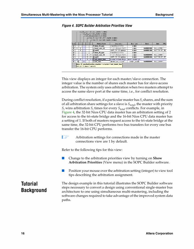
Figure 4. SOPC Builder Arbitration Priorities View
This view displays an integer for each master/slave connection. The integer value is the number of shares each master has for slave-access arbitration. The system only uses arbitration when two masters attempt to access the same slave port at the same time, i.e., for conflict resolution.
During conflict resolution, if a particular master has Si shares, and the sum of all arbitration share settings for a slave is Stotal, the master with priority Si wins arbitration Si times for every Stotal conflicts. For example, in Figure 4, the 32-bit Nios CPU data master has an arbitration setting of 2 for access to the tri-state bridge and the 16-bit Nios CPU data master has a setting of 1. If both of masters request access to the tri-state bridge at the same time, the 32-bit CPU performs two bus transfers for every one bus transfer the 16-bit CPU performs.
1 Arbitration settings for connections made in the master connections view are 1 by default.
Refer to the following tips for this view:
■ Change to the arbitration priorities view by turning on Show Arbitration Priorities (View menu) in the SOPC Builder software.
■ Position your mouse over the arbitration setting (integer) to view tool tips describing the arbitration assignment.
Tutorial Background
The design example in this tutorial illustrates the SOPC Builder software steps necessary to convert a design using conventional single-master bus architecture to one using simultaneous multi-mastering, including the software changes required to take advantage of the improved system data paths.
16 Altera Corporation
Background Simultaneous Multi-Mastering with the Nios Processor Tutorial
Background
2
This design is based on the standard 32-bit Ethernet reference design included with the Nios Ethernet Development Kit (EDK). In the tutorial, you will add a DMA peripheral to the system, define system interconnects used in the Avalon bus module, and modify the Ethernet MAC software drivers to use DMA.
Single-Master vs. Multi-Master Architectures
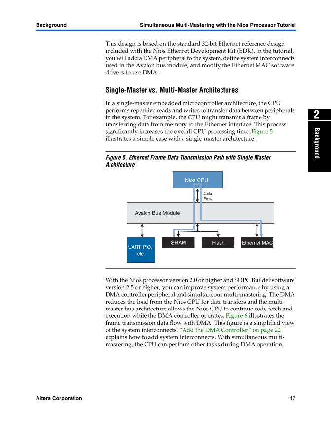
In a single-master embedded microcontroller architecture, the CPU performs repetitive reads and writes to transfer data between peripherals in the system. For example, the CPU might transmit a frame by transferring data from memory to the Ethernet interface. This process significantly increases the overall CPU processing time. Figure 5 illustrates a simple case with a single-master architecture.
Figure 5. Ethernet Frame Data Transmission Path with Single Master Architecture
With the Nios processor version 2.0 or higher and SOPC Builder software version 2.5 or higher, you can improve system performance by using a DMA controller peripheral and simultaneous multi-mastering. The DMA reduces the load from the Nios CPU for data transfers and the multi-master bus architecture allows the Nios CPU to continue code fetch and execution while the DMA controller operates. Figure 6 illustrates the frame transmission data flow with DMA. This figure is a simplified view of the system interconnects. “Add the DMA Controller” on page 22 explains how to add system interconnects. With simultaneous multi-mastering, the CPU can perform other tasks during DMA operation.
Nios CPU
UART, PIO, etc.
Avalon Bus Module
Flash Ethernet MACSRAM
DataFlow
Altera Corporation 17

Simultaneous Multi-Mastering with the Nios Processor Tutorial Background
Figure 6. Ethernet Frame Data Transmission Path Using DMA & Simultaneous Multi-Mastering Note (1)
Note:(1) To illustrate the data flow more clearly, details such as the DMA control slave and
tri-state bridges have been omitted from this figure. See Figure 13 on page 26 for a complete system block diagram.
Memory Usage
This tutorial is for users with a Nios development board and Nios EDK who want to download the finished design and operate it on the Nios board for evaluation purposes. Therefore, the tutorial design implements data and program memory in shared SRAM. During system operation the Nios CPU is nearly always fetching instructions from program memory while executing instructions in the CPU pipeline. Occasionally the CPU needs to load or store data from data memory, or communicate to a peripheral.
The design itself, and the capabilities of simultaneous multi-mastering, show even greater performance improvements if the system features separate program and data memories (i.e., a Harvard architecture). For example, while this tutorial design shows improved performance using a DMA controller and shared data and program memory, performance is still limited because arbitration occurs during simultaneous DMA transfers and the CPU fetches Nios instructions from the same memory.
Avalon Bus Module
Nios CPU
Instruction Master
Data Master
DMA Controller
Write Master
Read Master
ArbitratorUART, PIO,
etc.
Avalon Bus Module
Flash Ethernet MACSRAM
DataFlow
Avalon Bus Module
DataFlow
18 Altera Corporation

Background Simultaneous Multi-Mastering with the Nios Processor Tutorial
Background
2
For designs in which data memory is physically separate from instruction memory, this limitation does not exist. DMA transfers occur simultaneously, without any arbitration, along with CPU instruction fetches. Arbitration is not required during a DMA transfer unless the CPU performed a load or store to data memory, which occurs much less frequently than instruction fetching.
Because the Nios CPU has physically separate instruction and data masters that can be connected to any number of memory devices in the SOPC Builder software, you can implement either shared data and program memory as in this tutorial, or a Harvard architecture with separate data and program memory. You can implement a Harvard architecture on the Nios development board using an SRAM or SDRAM SODIMM-type card with the board. Additionally, some Altera programmable logic devices, such as Stratix™ devices, include large amounts of on-chip memory that can be used for even faster simultaneous multi-master designs.
Altera Corporation 19


Altera Corporation
Tutorial
Design Entry
2
The following tutorial guides you through the simultaneous multi-master design flow using the Quartus II software and SOPC Builder software. First, you will modify the hardware portion of the design using the SOPC Builder software. Next, you will modify the software portion of the design. Finally, the tutorial describes some methods for further optimizing your design.
f Refer to “Background” on page 13 for more information about the goals of this tutorial.
Hardware Modifications
In this section, you will use the SOPC Builder software and the Quartus II software to modify the Nios design by adding a DMA controller peripheral. Then, you will optimize the design for simultaneous multi-mastering. Finally, you will regenerate the Nios project and compile it.
Open the Quartus II Project
To start the Quartus II software and open the custom instruction project, follow these steps:
1. Choose Programs > Altera> Quartus II <version> (Windows Start menu) to start the Quartus II software.
2. Choose Open Project (File menu) to open the project.
3. Browse to the working directory of your project. This tutorial uses the following default directory:
c:\altera\excalibur\sopc_builder_2_5\tutorials\SMM_Tutorial
4. Select SMM_Tutorial.quartus and click Open. The top-level block diagram file for this project, SMM_Tutorial.bdf, appears. See Figure 7.
21

Simultaneous Multi-Mastering with the Nios Processor Tutorial Tutorial
Figure 7. SMM_Tutorial.bdf
Add the DMA Controller
To add the DMA controller to the design, perform the following steps:
1. Double-click the ref_system symbol in the SMM_Tutorial.bdf file to launch the SOPC Builder software. The SOPC Builder System Contents page displays.
The System Contents page lists peripherals that make up the example Ethernet design. Data flows to and from the Ethernet peripheral through the Avalon bridge nedk_card_bus. Therefore, the Nios CPU can only communicate with the Ethernet peripheral.
2. If the SOPC Builder software is not already in master connections mode, choose Master Connections (View menu). See Figure 8.
22 Altera Corporation

Tutorial Simultaneous Multi-Mastering with the Nios Processor Tutorial
Design Entry
2
Figure 8. Activating SOPC Builder Master Connections
3. Add a DMA controller peripheral to the design.
a. Click DMA under Other in the module pool on the left side of the System Contents page.
b. Click Add. The Avalon DMA Controller - dma_0 dialog box appears.
c. Set the maximum number of data items that can be processed in a single DMA command. Because the maximum Ethernet frame size is 1,500 bytes, specify 11 bits for the width of the DMA register. See Figure 9.
Figure 9. DMA Controller Peripheral Settings
Altera Corporation 23

Simultaneous Multi-Mastering with the Nios Processor Tutorial Tutorial
1 The DMA controller acts as a second master to the nedk_card_bus tri-state bridge, which is connected to the Ethernet interface. By modifying the software driver that connects to the Ethernet interface, you can use the DMA controller to handle data transfers between the Ethernet interface and memory, reducing CPU usage significantly.
d. Rename the DMA controller as eth_dma (see Figure 10).
Figure 10. Ethernet Design with DMA Controller
4. After you add the DMA controller, the system has two additional master ports (used for DMA reads and DMA writes) and one slave port (used for status and command communication with a CPU). The System Contents page shows eth_dma/read_master (avalon) and eth_dma/write_master (avalon) as master columns. Click the + icon next to eth_dma to display the eth_dma/control_port_slave slave.
Until you establish connections, the two master ports are not connected to the other masters and slaves in the system; therefore, the SOPC Builder software displays warning messages (see Figure 11). In contrast, the control slave port is connected automatically to the Nios CPU data master.
Figure 11. SOPC Builder Warnings for Disconnected DMA Controller Ports
24 Altera Corporation

Tutorial Simultaneous Multi-Mastering with the Nios Processor Tutorial
Design Entry
2
5. The DMA controller will transfer Ethernet frame data to and from the Ethernet interface. Therefore, you should connect both read and write masters to the Ethernet interface through its tri-state bridge, nedk_card_bus. Additionally, you should connect the DMA controller read and write masters to data memory, via the ext_mem_bus tri-state bridge, which stores the parsed Ethernet frames. These connections permit the Nios CPU to control DMA transfers of frame data directly to Ethernet from data memory or vice versa. (By default, the DMA control slave is connected to the Nios CPU data master, which permits read and write transfers of control and status information between the Nios CPU and the DMA controller.)
Make connections between the DMA controller bus (eth_dma/read_master (avalon) and eth_dma/write_master (avalon)), Ethernet interface (nedk_card_bus), memory (ext_mem_bus), and the Nios CPU by clicking the appropriate empty circles to the left of the peripheral names. After you click a circle, it displays as filled, indicating a connection (see Figure 12).
Figure 12. Making Bus Connections in the SOPC Builder Software
Figure 13 shows a detailed block diagram of the system interconnects for the system shown in Figure 12. Peripherals such as the UART, timer, and programmable I/Os (PIOs) were omitted for clarity (their bus connections are still present). During system generation, the SOPC Builder software automatically creates and connects the interconnects, multiplexers, and arbitration implemented in the shaded Avalon Bus Module region.
DMA Read & WriteMasters Connectedto Ethernet & Memory
Altera Corporation 25

Simultaneous Multi-Mastering with the Nios Processor Tutorial Tutorial
Figure 13. System Interconnect Block Diagram
You are finished adding the DMA controller peripheral. Next, you will optimize the design for simultaneous multi-master operation.
Optimize Simultaneous Multi-Master Operation
When you add peripherals, the default arbitration for each slave peripheral with multiple masters is equal, i.e., each master-slave pair has an arbitration setting of 1. Change the arbitration settings as described in the following steps:
1. Choose Show Arbitration Priorities (View menu).
2. Select the 1 in the column corresponding to cpu/instruction_master (avalon) and row corresponding to ext_mem_bus.
3. Type 4 r.
Nios CPU
Instruction Master
Data Master
DMA Controller
Write Master
Control Slave
Read Master
BootROM
Slave
SRAM & FlashInterfaces
Slave
EthernetInterface
Slave
MAC/PHY
Arbitrator Arbitrator
Multiplexer
Write Data & Control Signals
Read Data & Wait Signals
Tri-State Avalon Bus
Tri-State Bridge
Avalon Bus Module
FlashSRAM
Tri-State Bridge
Multiplexer MultiplexerMultiplexer
APEX Device
Off-Chip
26 Altera Corporation

Tutorial Simultaneous Multi-Mastering with the Nios Processor Tutorial
Design Entry
2
4. Repeat steps 2 and 3 for the column cpu/data_master (avalon) and row ext_mem_bus.
Figure 14 shows the arbitration settings for the multi-master Ethernet design.
Figure 14. Multi-Master Ethernet Design Arbitration Settings
f Refer to “Arbitration Priorities View” on page 15 for more details on making arbitration settings.
Connecting the buses as described in previous steps permits full operation of the Ethernet design with arbitration priorities for all masters set equally. You can further optimize the design by analyzing conflicts that require bus arbitration and changing the arbitration setting. This technique is useful for performance-critical applications.
For example, while the DMA controller transfers a frame to the Ethernet interface, the Nios CPU can initiate bus transfers without arbitration with other system peripherals via simultaneous multi-mastering. However, because the Nios development board has shared program and data memory (in SRAM), the performance of further code fetch and execution depends on the latency of access to this shared program/data memory. By customizing the arbitration settings between the Nios CPU and DMA controller for access to the shared program/data memory, you can further improve system performance while sending and receiving Ethernet frame data.
Altera Corporation 27

Simultaneous Multi-Mastering with the Nios Processor Tutorial Tutorial
If the Nios CPU instruction and data master has a higher arbitration priority, the CPU can fetch code and execute it through the shared memory resource. Consequently, the DMA controller has a higher latency to transfer an Ethernet frame. For example, a system could have an arbitration setting of 4 for the CPU instruction and data masters and 1 for the DMA controller as shown in Figure 14. Then, if a conflict arises in which a frame transmits while the CPU fetches instructions, the Nios CPU can issue 4 instruction fetches for every half-word transfer from the DMA controller to the Ethernet peripheral.
Figure 15 illustrates the data flow when a conflict between the DMA controller and Nios CPU arises. Each block represents a single bus transfer between master and slave.
Figure 15. Simplified View of Arbitration during Conflict between DMA & CPUThe Nios CPU instruction master and DMA controller read master both request continuous access to the shared SRAM.
1 Figure 15 illustrates a potential worst-case scenario in which the CPU instruction master and DMA read master both attempt to access shared SRAM for an extended period of time. This scenario might occur briefly because the CPU must periodically use its data master to read or write data as required, thus allowing higher DMA throughput.
When you are done making arbitration settings, you are ready to generate the Nios system module.
Nios CPU
Instruction Master
Data Master
DMA Controller
ReadMaster
WriteMaster
Arbitrator
Ethernet MAC
SRAM
DataFlow
DataFlow
Data Flow
28 Altera Corporation

Tutorial Simultaneous Multi-Mastering with the Nios Processor Tutorial
Design Entry
2
Generate the Nios System Module
To generate the Nios system module, perform the following steps:
1. Click the System Generation tab in the SOPC Builder software.
2. Make the following settings under Options in the System Generation tab:
– SDK: Turn on
1 For more information on the files that are generated in the SDK, refer to the Nios Embedded Processor Software Development Reference Manual.
– HDL: Turn on and choose Verilog and APEX 20KE
1 This tutorial uses a Verilog HDL top-level file. If you want to use VHDL, you should use the VHDL 32-bit standard Ethernet reference design as a starting point.
– Synthesis: Turn on and choose to optimize for area– Simulation: Turn on
3. Click Generate to build the system.
With the SDK option turned on, the SOPC Builder software automatically updates the cpu_sdk directory, which contains header files and software libraries for DMA operation. This update lets you compile the software that uses the DMA controller.
Compile the Quartus II Project
Once system generation has completed, you must compile the design in the Quartus II software before you can download it to the Nios development board. Perform the following steps when system generation completes:
1. Click Exit to close the SOPC Builder software.
2. Choose Start Compilation (Processing menu) in the Quartus II software to begin compilation.
When compilation completes, you have finished all hardware modifications necessary for the tutorial design. Next, you will modify the software drivers used to communicate with the Ethernet MAC device.
Altera Corporation 29

Simultaneous Multi-Mastering with the Nios Processor Tutorial Tutorial
Software Modifications
The following tutorial steps describe how to update the Ethernet MAC software drivers to work with the hardware modifications you made earlier in this tutorial. For other designs, you may need to make additional code modifications, e.g., if your system has software code that moves data between peripherals. These steps assume that you are familiar with the C programming language.
1 If you have the Nios EDK, follow the instructions in this section to modify the software drivers for the CS8900A Ethernet MAC device. If you have the Nios 10/100 EDK, open the lan91c111.c file to view the corresponding source code modifications for the LAN91C111 Ethernet MAC device. Altera provides this file with the tutorial design files, which you can download from the Nios literature page on the Altera web site at http://www.altera.com/literature/lit-nio.html.
1. Open the cs8900.c file located in the directory:
<installation path>\Altera\Excalibur\sopc_builder_2_5\tutorials\SMM_Tutorial\cpu_sdk\lib
2. Find the nr_cs8900_tx_frame routine in the cs8900.c file.
Figure 16 shows the CS8900A driver with a simple loop for transmitting Ethernet frames.
Figure 16. Simple Loop for Transmitting Frames
// Step 3: write the data out
// Half-word pointer to beginning of Ethernet framew = (r16 *)ethernet_frame;
// Begin code you should delete// While half-word frame segments remain, write out data to Ethernet MACwhile(frame_length_r16-- > 0){
// Read the next half-word of frame from memoryrd = *w++;
// Send half-word to Ethernet MAC data buffere->np_cs8900iodata0 = rd;
}// End code you should delete
30 Altera Corporation

Tutorial Simultaneous Multi-Mastering with the Nios Processor Tutorial
Design Entry
2
You can replace this code with a call to a predefined DMA function, nr_dma_copy_range_to_1, which the SOPC Builder software automatically includes in the SDK when you add a DMA controller to a system. This function configures the DMA controller to copy data from a range of source addresses to a single destination address and then starts the DMA transfer. In this example, the function copies data from a range of data memory (beginning with a pointer to the Ethernet frame) to a single address on the external Ethernet MAC (the Ethernet MAC data register).
1 Refer to the Nios Embedded Processor Peripherals Reference Manual for more information on DMA controller software routines.
3. In the cs8900.c file, replace the loop code shown in Figure 16 with the code shown in Figure 17. The code shown in Figure 17 waits for any pending DMA transfers to complete before calling nr_dma_copy_range_to_1.
Figure 17. DMA Routine for Transmitting Frames
// Step 3: write the data out
// Half-word pointer to the data outw = (r16 *)ethernet_frame;
// Begin new SMM tutorial DMA code{
// Declare "ethDMA" as pointer to "eth_dma" np_dma *ethDMA = na_eth_dma;
// Wait for any pending DMA transfers to completewhile(!(ethDMA->np_dmastatus & np_dmastatus_done_mask) && ethDMA->np_dmastatus != 0);
// Perform DMA transfernr_dma_copy_range_to_1(na_eth_dma, 2, (void *)w, (void *)&e->np_cs8900iodata0,
frame_length);}// End new SMM tutorial DMA code
4. After adding the DMA routine to the nr_cs8900_tx_frame function to accelerate data transmission, modify the software routine that handles receiving frames from Ethernet to support DMA. Locate the nr_cs8900_check_for_events function in the cs8900.c file. See Figure 18.
Altera Corporation 31

Simultaneous Multi-Mastering with the Nios Processor Tutorial Tutorial
Figure 18. Simple Loop for Receiving FramesOriginal source code comments have been removed and replaced for clarity in this tutorial. The actual code is identical.
// Half-word pointer to the receive data bufferw = g_frame_buffer;
// Begin the code that you should delete// For the entire frame length (which is read from the CS8900)for(i = 0; i < frame_length_r16; i ++){
// Read the CS8900 data bufferrd = e->np_cs8900iodata0;
// Increment the read pointer*w++ = rd;
}// End code that you should delete
5. In the cs8900.c file, replace the loop shown in Figure 18 with the code shown in Figure 19. The code shown in Figure 19 waits for any pending DMA transfers to complete before calling nr_dma_copy_1_to_range. This function is the inverse of the one used in step 3; it copies received Ethernet data from a fixed address (CS8900 data address) to a range of addresses (memory range of the Nios data memory).
Figure 19. DMA Routine to Receive Frames
// Half-word pointer to the receive data bufferw = g_frame_buffer;
// Begin new SMM tutorial DMA code{
// Declare "ethDMA" as pointer to "eth_dma" np_dma *ethDMA = na_eth_dma;
// Wait for any pending DMA transfers to completewhile(!(ethDMA->np_dmastatus & np_dmastatus_done_mask) && ethDMA->np_dmastatus != 0);
// Perform DMA transfernr_dma_copy_1_to_range(na_eth_dma, 2, (void *)&e->np_cs8900iodata0, (void *)w,
frame_length);}// End new SMM tutorial DMA code
6. Save your changes to the cs8900.c file.
7. Open the file dma.c, which is located in the SMM_Tutorial\nios_cpu\lib directory. The dma.c file contains the predefined routines used in steps 3 and 5.
32 Altera Corporation

Tutorial Simultaneous Multi-Mastering with the Nios Processor Tutorial
Design Entry
2
8. To ensure that each DMA transfer completes, the file waits for the DMA to finish before returning to the user’s code. Because the code changes in steps 3 and 5 poll the DMA controller’s status register to verify that the previous transfer is complete, you can enhance performance slightly by removing this wait.
In the dma.c dma_shared function, comment out the wait routine near the end of the function (see Figure 20):
Figure 20. Comment Out Wait Routine
// |// | 4. Wait until it’s all done// |
/*while((dma->np_dmastatus & np_dmastatus_busy_mask) != 0)
;*/
return;
9. Save your changes to the dma.c file.
1 You are finished making changes to the source code for this tutorial. You can make additional improvements by using DMA instead of other application code in which a loop transfers data, e.g., in file system operation and network protocol stacks. “Appendix—TCP/IP Stack Code Changes” on page 35 includes selected source code showing similar modifications to the Nios EDK TCP/IP stack (the entire source comes with the kit).
10. Compile the software source code.
1 You must compile changes to software source code, such as the cs8900.c file, located in the SDK lib directory separately from the source files located in the SDK src directory.
a. At a Command Prompt, change to the directory <path>\SMM_Tutorial\cpu_sdk\lib.
b. Type the following command to rebuild all library files including cs8900.c and dma.c:
make -s all r
Altera Corporation 33

Simultaneous Multi-Mastering with the Nios Processor Tutorial Tutorial
1 If you regenerate your system using the SOPC Builder software, the cs8900.c and dma.c files in the cpu_sdk\lib directory are overwritten and the changes you made are lost. If you want to regenerate your system and save your changes to these files, copy the cpu_sdk directory to a new location, e.g., my_sdk.
c. When the library is finished building, compile your source files that use the Ethernet interface (cs8900.c) or the TCP/IP stack (plugs.c) to use the enhancements you made in this tutorial. For example, if you use the hello_plugs or nedk_example_web_server application, you should recompile the application using nios-build.
1 Because these changes only affect the performance of CS8900 driver, not its functionality, existing applications using the Nios Ethernet Development Kit receive performance benefits without additional software modifications. You need to rebuild only the existing source code to include the updated library information.
You are finished making the software changes. You can download the design to the Nios development board to check the performance improvements.
Next Steps Congratulations! You have completed the simultaneous multi-mastering tutorial. You can make further optimizations using DMA and simultaneous multi-mastering by analyzing the dataflow elsewhere in the system.
Altera provides a completed example based on the system described in this tutorial. You can run the example on the Nios development board with the Ethernet kit daughter card attached. This example includes an executable S-record (.srec) file that runs the web server application—including additional software optimizations using the DMA controller and the system created in this tutorial design—a flash programming file (.flash) with web server content, and profiling code included with the web server to measure throughput with and without the simultaneous multi-master optimizations. By serving up images on the web server application with multi-master optimizations in place, the design more than doubles the throughput of a 60 kb image.
f Refer to the readme.txt file provided with the tutorial example files for more information on how to download and run the completed tutorial design.
34 Altera Corporation

Altera Corporation
Appendix—TCP/IP StackCode Changes
Appendix
3
This appendix contains additional source code modification examples that use a DMA controller with the simultaneous multi-master tutorial design.
Packet Payload Appending Function
This packet payload appending function, packet_append_bytes, is located in the plugs.c file, which is the Nios EDK TCP/IP stack. The function appends the packet payload to a partially constructed TCP/IP packet. In the original source code, the function copies the data with the Nios CPU. In the modified code, the DMA controller copies the packet payload. Figures 21 and 22 show the original and modified source code, respectively.
Figure 21. packet_append_bytes Original Source Code
void packet_append_bytes(char **dst,void *src, int length){
char *src_c = (char *)src;char *w = *dst;
while(length--)*w++ = *src_c++;
*dst = w;}
35

Simultaneous Multi-Mastering with the Nios Processor Tutorial Appendix—TCP/IP Stack Code Changes
Figure 22. packet_append_bytes Modified Source Code
void packet_append_bytes(char **dst,void *src, int length){
char *src_c = (char *)src;char *w = *dst;
// Begin SMM tutorial modifcation{
// Declare ethDMA as pointer to eth_dmanp_dma *ethDMA = na_eth_dma;
// Wait for any pending DMA transfers to completewhile(!(ethDMA->np_dmastatus & np_dmastatus_done_mask) &&
ethDMA->np_dmastatus != 0);
// Perform DMA transfernr_dma_copy_range_to_range(na_eth_dma, 1, ((void*)src_c),
((void*)w), length);
// dst pointer must be properly set in original function// w was incremented by length in the while loop*dst = w + length;
}// End SMM tutorial modification
}
r_tcp_send Function
The r_tcp_send function is located in the plugs.c file, which is the Nios EDK TCP/IP stack. The code calls this function after the user sends a TCP packet to the plugs library using the nr_plugs_send function, and is part of the TCP packet assembly process. Figures 23 and 24 show the original and modified source code, respectively.
Figure 23. r_tcp_send Original Source Code Excerpt
// | If SYN or FIN, bump our local seq by 1,// | else, if PSH, put payload bump local seq by payload size
if(tcp_flags & (ne_plugs_flag_tcp_syn | ne_plugs_flag_tcp_fin))plug->tcp_sn_local++;
else if(tcp_flags & ne_plugs_flag_tcp_psh){
// |// | Copy the payload (byte by byte) // |
int i;
plug->tcp_sn_local += payload_length;for(i = 0; i < payload_length; i++)
tcp_reply->payload[i] = ((char *)payload)[i];}
36 Altera Corporation

Appendix—TCP/IP Stack Code Changes Simultaneous Multi-Mastering with the Nios Processor Tutorial
Appendix
3
Figure 24. r_tcp_send Modified Source Code
if(tcp_flags & (ne_plugs_flag_tcp_syn | ne_plugs_flag_tcp_fin))plug->tcp_sn_local++;
else if(tcp_flags & ne_plugs_flag_tcp_psh){
plug->tcp_sn_local += payload_length;
// Begin SMM tutorial modifcation{
// Payload length is in bytes... Convert to half words and speed things upint payload_length_hw = (payload_length + 1) / 2;
// Declare ethDMA as pointer to eth_dmanp_dma *ethDMA = na_eth_dma;
// Wait for pending DMA transfers to completewhile(!(ethDMA->np_dmastatus & np_dmastatus_done_mask) &&
ethDMA->np_dmastatus != 0);
// Perform DMA transfernr_dma_copy_range_to_range(na_eth_dma, 2, (void*)payload,
(void*)tcp_reply->payload, payload_length_hw);}// End SMM tutorial modification
}
Altera Corporation 37
