single-/dual-supply, high voltage isolated igbt gate ... · single-/dual-supply, high voltage...
TRANSCRIPT
Single-/Dual-Supply, High Voltage Isolated IGBT Gate Driver
Data Sheet ADuM4136
Rev. 0 Document Feedback Information furnished by Analog Devices is believed to be accurate and reliable. However, no responsibility is assumed by Analog Devices for its use, nor for any infringements of patents or other rights of third parties that may result from its use. Specifications subject to change without notice. No license is granted by implication or otherwise under any patent or patent rights of Analog Devices. Trademarks and registered trademarks are the property of their respective owners.
One Technology Way, P.O. Box 9106, Norwood, MA 02062-9106, U.S.A.Tel: 781.329.4700 ©2016 Analog Devices, Inc. All rights reserved. Technical Support www.analog.com
FEATURES 4 A peak drive output capability Output power device resistance: <1 Ω Desaturation protection
Isolated fault output Soft shutdown on fault
Isolated fault and ready functions Low propagation delay: 55 ns typical Minimum pulse width: 50 ns Operating temperature range: −40°C to +125°C Output voltage range to 35 V Input voltage range from 2.5 V to 6 V Output and input undervoltage lockout (UVLO) Creepage distance: 7.8 mm minimum 100 kV/μs minimum common-mode transient immunity (CMTI) 20-year lifetime for 600 V rms or 1092 V dc working voltage Safety and regulatory approvals (pending)
5 kV ac for 1 minute per UL 1577 CSA Component Acceptance Notice 5A DIN V VDE V 0884-10 (VDE V 0884-10):2006-12
VIORM = 849 V peak (basic)
APPLICATIONS MOSFET/IGBT gate drivers Photovoltaic (PV) inverters Motor drives Power supplies
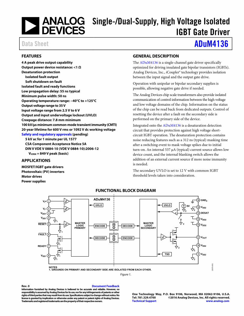
GENERAL DESCRIPTION The ADuM4136 is a single-channel gate driver specifically optimized for driving insulated gate bipolar transistors (IGBTs). Analog Devices, Inc., iCoupler® technology provides isolation between the input signal and the output gate drive.
Operation with unipolar or bipolar secondary supplies is possible, allowing negative gate drive if needed.
The Analog Devices chip scale transformers also provide isolated communication of control information between the high voltage and low voltage domains of the chip. Information on the status of the chip can be read back from dedicated outputs. Control of resetting the device after a fault on the secondary side is performed on the primary side of the device.
Integrated onto the ADuM4136 is a desaturation detection circuit that provides protection against high voltage short-circuit IGBT operation. The desaturation protection contains noise reducing features such as a 312 ns (typical) masking time after a switching event to mask voltage spikes due to initial turn-on. An internal 537 μA (typical) current source allows low device count, and the internal blanking switch allows the addition of an external current source if more noise immunity is needed.
The secondary UVLO is set to 12 V with common IGBT threshold levels taken into consideration.
FUNCTIONAL BLOCK DIAGRAM
MASTERLOGIC
PRIMARY
GND2VI+
VI–
READY
1
2
7
16
VSS215
VSS1 4
VSS1 8
FAULT 6
VDD1 3
MASTERLOGIC
SECONDARY
UVLOUVLO
TSD
ENCODE
DECODE
DECODE
ENCODE VOUT11
VSS29
VSS210
VDD213
VDD212RESET 5
9V
DESAT14
ADuM4136
NOTES1. GROUNDS ON PRIMARY AND SECONDARY SIDE ARE ISOLATED FROM EACH OTHER. 13
575-
001
1
1
1
1
1
22
2
22
2
Figure 1.
ADuM4136 Data Sheet
Rev. 0 | Page 2 of 16
TABLE OF CONTENTS Features .............................................................................................. 1
Applications ....................................................................................... 1
General Description ......................................................................... 1
Functional Block Diagram .............................................................. 1
Revision History ............................................................................... 2
Specifications ..................................................................................... 3
Electrical Characteristics ............................................................. 3
Package Characteristics ............................................................... 4
Regulatory Information ............................................................... 4
Insulation and Safety Related Specifications ............................ 4
DIN V VDE V 0884-10 (VDE V 0884-10) Insulation Characteristics .............................................................................. 5
Recommended Operating Conditions ...................................... 5
Absolute Maximum Ratings ............................................................ 6
ESD Caution...................................................................................6
Pin Configuration and Function Descriptions ..............................7
Typical Performanace Characteristics ............................................8
Applications Information .............................................................. 11
PCB Layout ................................................................................. 11
Propagation Delay Related Parameters ................................... 11
Protection Features .................................................................... 11
Power Dissipation....................................................................... 13
DC Correctness and Magnetic Field Immunity ........................... 13
Insulation Lifetime ..................................................................... 13
Typical Application .................................................................... 15
Outline Dimensions ....................................................................... 16
Ordering Guide .......................................................................... 16
REVISION HISTORY 7/2016—Revision 0: Initial Version
Data Sheet ADuM4136
Rev. 0 | Page 3 of 16
SPECIFICATIONS ELECTRICAL CHARACTERISTICS Low-side voltages are referenced to VSS1. High-side voltages are referenced to GND2; 2.5 V ≤ VDD1 ≤ 6 V, 12 V ≤ VDD2 ≤ 35 V, and TJ = −40°C to +125°C. All minimum/maximum specifications apply over the entire recommended operating range, unless otherwise noted. All typical specifications are at TJ = 25°C, VDD1 = 5.0 V, VSS2 = 0 V, and VDD2 = 15 V.
Table 1. Parameter Symbol Min Typ Max Unit Test Conditions/Comments DC SPECIFICATIONS
High-Side Power Supply Input Voltage
VDD2 VDD2 12 35 V VDD2 − VSS2 ≤ 35 V VSS2 VSS2 −15 0 V
Input Current, Quiescent Ready high VDD2 IDD2 (Q) 3.62 4.49 mA VSS2 ISS2 (Q) 4.82 6.21 mA
Logic Supply VDD1 Input Voltage VDD1 2.5 6 V Input Current IDD1
Output Low 1.78 2.17 mA Output signal low Output High 4.78 5.89 mA Output signal high
Logic Inputs (VI+, VI−, RESET)
Input Current (VI+, VI− Only) II −1 +0.01 +1 μA Input Voltage
Logic High VIH 0.7 × VDD1 V 2.5 V ≤ VDD1 − VSS1 ≤ 5 V 3.5 V VDD1 − VSS1 > 5 V Logic Low VIL 0.3 × VDD1 V 2.5 V ≤ VDD1 − VSS1 ≤ 5 V 1.5 V VDD1 − VSS1 > 5 V
RESET Internal Pull-Down RRESET_PD 300 kΩ
Undervoltage Lockout (UVLO) VDD1
Positive Going Threshold VVDD1UV+ 2.43 2.49 V Negative Going Threshold VVDD1UV− 2.29 2.34 V Hysteresis VVDD1UVH 0.09 V
VDD2 Positive Going Threshold VVDD2UV+ 11.6 12.0 V Negative Going Threshold VVDD2UV− 10.4 11.2 V Hysteresis VVDD2UVH 0.4 V
FAULT Pull-Down FET Resistance RFAULT_PD_FET 11 50 Ω Tested at 5 mA
READY Pull-Down FET Resistance RRDY_PD_FET 11 50 Ω Tested at 5 mA Desaturation (DESAT)
Desaturation Detect Comparator Voltage VDESAT, TH 8.66 9.2 9.57 V Internal Current Source IDESAT_SRC 466 537 592 μA
Thermal Shutdown (TSD) TSD Positive Edge TTSD_POS 155 °C TSD Hysteresis TTSD_HYST 20 °C
Internal NMOS Gate On Resistance RDSON_N 322 625 mΩ Tested at 250 mA 325 625 mΩ Tested at 1 A Internal PMOS Gate On Resistance RDSON_P 475 975 mΩ Tested at 250 mA 480 975 mΩ Tested at 1 A Soft Shutdown NMOS On Resistance RDSON_FAULT 10.4 22 Ω Tested at 250 mA Peak Current 4.61 A VDD2 = 12 V, 2 Ω gate resistance
SWITCHING SPECIFICATIONS Pulse Width1 PW 50 ns CL = 2 nF, VDD2 = 15 V, RGON
2 = RGOFF2 = 3.9 Ω
RESET Debounce tDEB_RESET 500 615 700 ns
ADuM4136 Data Sheet
Rev. 0 | Page 4 of 16
Parameter Symbol Min Typ Max Unit Test Conditions/Comments Propagation Delay3 tDHL, tDLH 40 55 68 ns CL = 2 nF, VDD2 = 15 V, RGON
2 = RGOFF2 = 3.9 Ω
Propagation Delay Skew4 tPSK 15 ns CL = 2 nF, RGON2 = RGOFF
2 = 3.9 Ω Output Rise/Fall Time (10% to 90%) tR/tF 11 16 22.9 ns CL = 2 nF, VDD2 = 15 V, RGON
2 = RGOFF2 = 3.9 Ω
Blanking Capacitor Discharge Switch Masking tDESAT_DELAY 213 312 615 ns Time to Report Desaturation Fault to FAULT Pin tREPORT 1.3 2 μs
Common-Mode Transient Immunity (CMTI) |CM| Static CMTI5 100 kV/μs VCM = 1500 V Dynamic CMTI6 100 kV/μs VCM = 1500 V
1 The minimum pulse width is the shortest pulse width at which the specified timing parameter is guaranteed. 2 See the Power Dissipation section. 3 tDLH propagation delay is measured from the time of the input rising logic high threshold, VIH, to the output rising 10% threshold of the VOUT signal. tDHL propagation delay is
measured from the input falling logic low threshold, VIL, to the output falling 90% threshold of the VOUT signal. See Figure 22 for waveforms of propagation delay parameters. 4 tPSK is the magnitude of the worst case difference in tDLH and/or tDHL that is measured between units at the same operating temperature, supply voltages, and output
load within the recommended operating conditions. See Figure 22 for waveforms of propagation delay parameters. 5 Static common-mode transient immunity is defined as the largest dv/dt between VSS1 and VSS2 with inputs held either high or low such that the output voltage remains
either above 0.8 × VDD2 for output high, or 0.8 V for output low. Operation with transients above the recommended levels can cause momentary data upsets. 6 Dynamic common-mode transient immunity is defined as the largest dv/dt between VSS1 and VSS2 with the switching edge coincident with the transient test pulse.
Operation with transients above the recommended levels can cause momentary data upsets.
PACKAGE CHARACTERISTICS
Table 2. Parameter Symbol Min Typ Max Unit Test Conditions/Comments Resistance (Input Side to High-Side Output)1 RI-O 1012 Ω Capacitance (Input Side to High-Side Output)1 CI-O 2.0 pF Input Capacitance CI 4.0 pF Junction to Ambient Thermal Resistance θJA 75.4 °C/W 4-layer printed circuit board (PCB) Junction to Case Thermal Resistance θJC 35.4 °C/W 4-layer PCB 1 The device is considered a two-terminal device: Pin 1 through Pin 8 are shorted together, and Pin 9 through Pin 16 are shorted together.
REGULATORY INFORMATION The ADuM4136 is pending approval by the organizations listed in Table 3.
Table 3. UL (Pending) CSA (Pending) VDE (Pending) Recognized under UL 1577
Component Recognition Program1 Approved under CSA Component Acceptance Notice 5A Certified according to VDE0884-102
Single Protection, 5000 V rms Isolation Voltage
Basic insulation per CSA 60950-1-07+A1+A2 and IEC 60950-1 2nd Ed.+A1+A2, 780 V rms (1103 V peak) maximum working voltage
Basic insulation, 849 V peak
CSA 60950-1-07+A1+A2 and IEC 60950-1 Second Ed.+A1+A2, 390 V rms (551 V peak) maximum working voltage
File E214100 File 205078 File 2471900-4880-0001 1 In accordance with UL 1577, each ADuM4136 is proof tested by applying an insulation test voltage ≥ 6000 V rms for 1 second (current leakage detection limit = 10 μA). 2 In accordance with DIN V VDE V 0884-10, each ADuM4136 is proof tested by applying an insulation test voltage ≥ 1590 V peak for 1 second (partial discharge
detection limit = 5 pC). An asterisk (*) marking branded on the component designates DIN V VDE V 0884-10 approval.
INSULATION AND SAFETY RELATED SPECIFICATIONS
Table 4. Parameter Symbol Value Unit Test Conditions/Comments Rated Dielectric Insulation Voltage 5000 V rms 1-minute duration Minimum External Air Gap (Clearance) L(I01) 7.8 min mm Measured from input terminals to output terminals, shortest
distance through air Minimum External Tracking (Creepage) L(I02) 7.8 min mm Measured from input terminals to output terminals, shortest
distance path along body Minimum Internal Gap (Internal Clearance) 0.026 min mm Insulation distance through insulation Tracking Resistance (Comparative Tracking Index) CTI >400 V DIN IEC 112/VDE 0303 Part 1 Isolation Group II Material Group (DIN VDE 0110, 1/89, Table 1)
Data Sheet ADuM4136
Rev. 0 | Page 5 of 16
DIN V VDE V 0884-10 (VDE V 0884-10) INSULATION CHARACTERISTICS Maintenance of the safety data is ensured by protective circuits. The asterisk (*) marking on the package denotes DIN V VDE V 0884-10 approval for a 560 V peak working voltage.
Table 5. VDE Characteristics Description Test Conditions/Comments Symbol Characteristic Unit Installation Classification per DIN VDE 0110
For Rated Mains Voltage ≤ 150 V rms I to IV For Rated Mains Voltage ≤ 300 V rms I to III For Rated Mains Voltage ≤ 400 V rms I to II
Climatic Classification 40/105/21 Pollution Degree per DIN VDE 0110, Table 1 2 Maximum Working Insulation Voltage VIORM 849 V peak Input to Output Test Voltage, Method B1 VIORM × 1.875 = Vpd (m), 100% production test, tini = tm = 1 sec,
partial discharge < 5 pC Vpd (m) 1592 V peak
Input to Output Test Voltage, Method A After Environmental Tests Subgroup 1 VIORM × 1.5 = Vpd (m), tini = 60 sec, tm = 10 sec, partial
discharge < 5 pC Vpd (m) 1274 V peak
After Input and/or Safety Test Subgroup 2 and Subgroup 3
VIORM × 1.2 = Vpd (m), tini = 60 sec, tm = 10 sec, partial discharge < 5 pC
Vpd (m) 1019 V peak
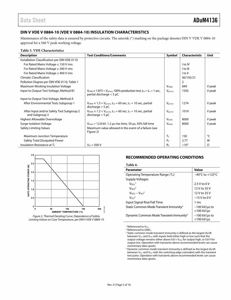
Highest Allowable Overvoltage VIOTM 8000 V peak Surge Isolation Voltage VPEAK = 12.8 kV, 1.2 μs rise time, 50 μs, 50% fall time VIOSM 8000 V peak Safety Limiting Values Maximum value allowed in the event of a failure (see
Figure 2)
Maximum Junction Temperature TS 150 °C Safety Total Dissipated Power PS 2.77 W
Insulation Resistance at TS VIO = 500 V RS >109 Ω
SA
FE
OP
ER
AT
ING
PO
WE
R (
W)
AMBIENT TEMPERATURE (°C)
0 50
3.0
2.5
2.0
1.5
1.0
0.5
0100 150 200
1357
5-00
2
Figure 2. Thermal Derating Curve, Dependence of Safety
Limiting Values on Case Temperature, per DIN V VDE V 0884-10
RECOMMENDED OPERATING CONDITIONS
Table 6. Parameter Value Operating Temperature Range (TA) −40°C to +125°C Supply Voltages
VDD11 2.5 V to 6 V
VDD22 12 V to 35 V
VDD2 − VSS22 12 V to 35 V
VSS22 −15 V to 0 V
Input Signal Rise/Fall Time 1 ms Static Common Mode Transient Immunity3 −100 kV/μs to
+100 kV/μs Dynamic Common Mode Transient Immunity4 −100 kV/μs to
+100 kV/μs 1 Referenced to VSS1. 2 Referenced to GND2. 3 Static common-mode transient immunity is defined as the largest dv/dt
between VSS1 and VSS2 with inputs held either high or low such that the output voltage remains either above 0.8 × VDD2 for output high, or 0.8 V for output low. Operation with transients above recommended levels can cause momentary data upsets.
4 Dynamic common-mode transient immunity is defined as the largest dv/dt between VSS1 and VSS2 with the switching edge coincident with the transient test pulse. Operation with transients above recommended levels can cause momentary data upsets.
ADuM4136 Data Sheet
Rev. 0 | Page 6 of 16
ABSOLUTE MAXIMUM RATINGS Table 7. Parameter Rating Storage Temperature Range (TST) −55°C to +150°C Junction Operating Temperature Range (TJ) −40°C to +125°C Supply Voltage
VDD1 to VSS1 −0.3 V to +6.5 V VDD2 to GND2 −0.3 V to +40 V VSS2 to GND2 −20 V to +0.3 V VDD2 − VSS2 40 V
Input Voltage VDESAT
1 −0.3 V to VDD2 + 0.3 V VI+,2 VI−,2 RESET2 −0.3 V to +6.5 V
Output Voltage VOUT
3 −0.3 V to VDD2 + 0.3 V Common-Mode Transients (|CM|) −150 kV/μs to
+150 kV/μs 1 Referenced to GND2. 2 Referenced to VSS1. 3 Referenced to VSS2.
Stresses at or above those listed under Absolute Maximum Ratings may cause permanent damage to the product. This is a stress rating only; functional operation of the product at these or any other conditions above those indicated in the operational section of this specification is not implied. Operation beyond the maximum operating conditions for extended periods may affect product reliability.
Table 8. Maximum Continuous Working Voltage1 Parameter Value Constraint 60 Hz AC Voltage 600 V rms 20-year lifetime at 0.1%
failure rate, zero average voltage
DC Voltage 1092 V peak Limited by the creepage of the package, Pollution Degree 2, Material Group II2, 3
1 See the Insulation Lifetime section for details. 2 Other pollution degree and material group requirements yield a different limit. 3 Some system level standards allow components to use the printed wiring
board (PWB) creepage values. The supported dc voltage may be higher for those standards.
ESD CAUTION
Table 9. Truth Table (Positive Logic)1 VI+ Input VI− Input RESET Pin READY Pin FAULT Pin VDD1 State VDD2 State VGATE
2 L L H H H Powered Powered L L H H H H Powered Powered L H L H H H Powered Powered H H H H H H Powered Powered L X X H L Unknown Powered Powered L X X H Unknown L Powered Powered L L L H L Unknown Unpowered Powered L X X L3 Unknown H3 Powered Powered L X X X L Unknown Powered Unpowered Unknown 1 L is low, H is high, and X is don’t care. 2 VGATE is the voltage of the gate being driven. 3 Time dependent value. See Figure 22 for details on timing.
Data Sheet ADuM4136
Rev. 0 | Page 7 of 16
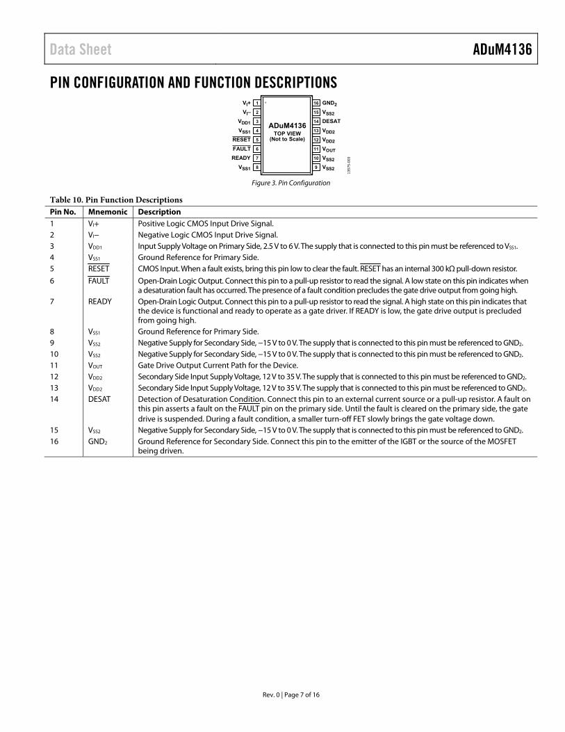
PIN CONFIGURATION AND FUNCTION DESCRIPTIONS VI+ 1
VI– 2
VDD1 3
VSS1 4
GND216
VSS215
DESAT14
VDD213
RESET 5 VDD212
FAULT 6 VOUT11
READY 7 VSS210
VSS1 8 VSS29
ADuM4136TOP VIEW
(Not to Scale)
1357
5-00
3
Figure 3. Pin Configuration
Table 10. Pin Function Descriptions Pin No. Mnemonic Description 1 VI+ Positive Logic CMOS Input Drive Signal. 2 VI− Negative Logic CMOS Input Drive Signal. 3 VDD1 Input Supply Voltage on Primary Side, 2.5 V to 6 V. The supply that is connected to this pin must be referenced to VSS1. 4 VSS1 Ground Reference for Primary Side. 5 RESET CMOS Input. When a fault exists, bring this pin low to clear the fault. RESET has an internal 300 kΩ pull-down resistor.
6 FAULT Open-Drain Logic Output. Connect this pin to a pull-up resistor to read the signal. A low state on this pin indicates when a desaturation fault has occurred. The presence of a fault condition precludes the gate drive output from going high.
7 READY Open-Drain Logic Output. Connect this pin to a pull-up resistor to read the signal. A high state on this pin indicates that the device is functional and ready to operate as a gate driver. If READY is low, the gate drive output is precluded from going high.
8 VSS1 Ground Reference for Primary Side. 9 VSS2 Negative Supply for Secondary Side, −15 V to 0 V. The supply that is connected to this pin must be referenced to GND2. 10 VSS2 Negative Supply for Secondary Side, −15 V to 0 V. The supply that is connected to this pin must be referenced to GND2. 11 VOUT Gate Drive Output Current Path for the Device. 12 VDD2 Secondary Side Input Supply Voltage, 12 V to 35 V. The supply that is connected to this pin must be referenced to GND2. 13 VDD2 Secondary Side Input Supply Voltage, 12 V to 35 V. The supply that is connected to this pin must be referenced to GND2. 14 DESAT Detection of Desaturation Condition. Connect this pin to an external current source or a pull-up resistor. A fault on
this pin asserts a fault on the FAULT pin on the primary side. Until the fault is cleared on the primary side, the gate drive is suspended. During a fault condition, a smaller turn-off FET slowly brings the gate voltage down.
15 VSS2 Negative Supply for Secondary Side, −15 V to 0 V. The supply that is connected to this pin must be referenced to GND2. 16 GND2 Ground Reference for Secondary Side. Connect this pin to the emitter of the IGBT or the source of the MOSFET
being driven.
ADuM4136 Data Sheet
Rev. 0 | Page 8 of 16
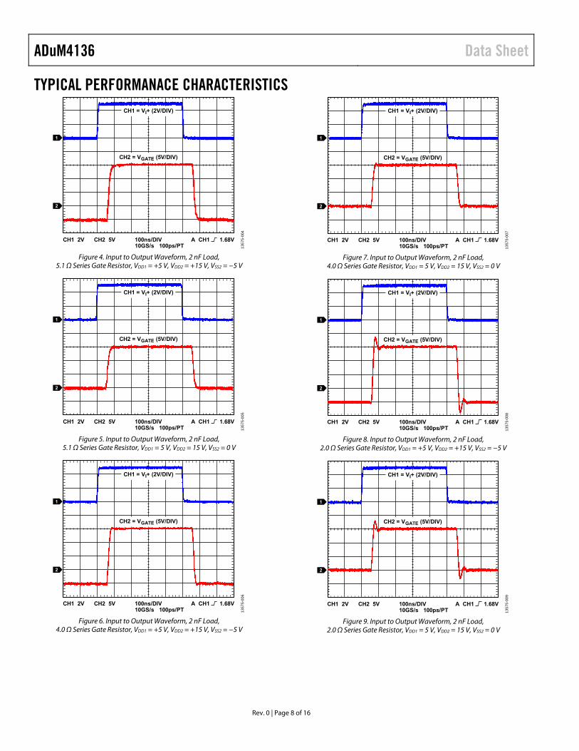
TYPICAL PERFORMANACE CHARACTERISTICS
CH1 2V CH2 5V 100ns/DIV
CH1 = VI+ (2V/DIV)
CH2 = VGATE (5V/DIV)
10GS/s 100ps/PTA CH1 1.68V
1
2
1357
5-00
4
Figure 4. Input to Output Waveform, 2 nF Load, 5.1 Ω Series Gate Resistor, VDD1 = +5 V, VDD2 = +15 V, VSS2 = −5 V
CH1 2V CH2 5V 100ns/DIV
CH1 = VI+ (2V/DIV)
CH2 = VGATE (5V/DIV)
10GS/s 100ps/PTA CH1 1.68V
1
2
1357
5-00
5
Figure 5. Input to Output Waveform, 2 nF Load, 5.1 Ω Series Gate Resistor, VDD1 = 5 V, VDD2 = 15 V, VSS2 = 0 V
CH1 2V CH2 5V 100ns/DIV
CH1 = VI+ (2V/DIV)
CH2 = VGATE (5V/DIV)
10GS/s 100ps/PTA CH1 1.68V
1
2
1357
5-00
6
Figure 6. Input to Output Waveform, 2 nF Load, 4.0 Ω Series Gate Resistor, VDD1 = +5 V, VDD2 = +15 V, VSS2 = −5 V
CH1 2V CH2 5V 100ns/DIV
CH1 = VI+ (2V/DIV)
CH2 = VGATE (5V/DIV)
10GS/s 100ps/PTA CH1 1.68V
1
2
1357
5-00
7
Figure 7. Input to Output Waveform, 2 nF Load, 4.0 Ω Series Gate Resistor, VDD1 = 5 V, VDD2 = 15 V, VSS2 = 0 V
CH1 2V CH2 5V 100ns/DIV
CH1 = VI+ (2V/DIV)
CH2 = VGATE (5V/DIV)
10GS/s 100ps/PTA CH1 1.68V
1
2
1357
5-00
8
Figure 8. Input to Output Waveform, 2 nF Load, 2.0 Ω Series Gate Resistor, VDD1 = +5 V, VDD2 = +15 V, VSS2 = −5 V
CH1 2V CH2 5V 100ns/DIV
CH1 = VI+ (2V/DIV)
CH2 = VGATE (5V/DIV)
10GS/s 100ps/PTA CH1 1.68V
1
2
1357
5-00
9
Figure 9. Input to Output Waveform, 2 nF Load, 2.0 Ω Series Gate Resistor, VDD1 = 5 V, VDD2 = 15 V, VSS2 = 0 V
Data Sheet ADuM4136
Rev. 0 | Page 9 of 16
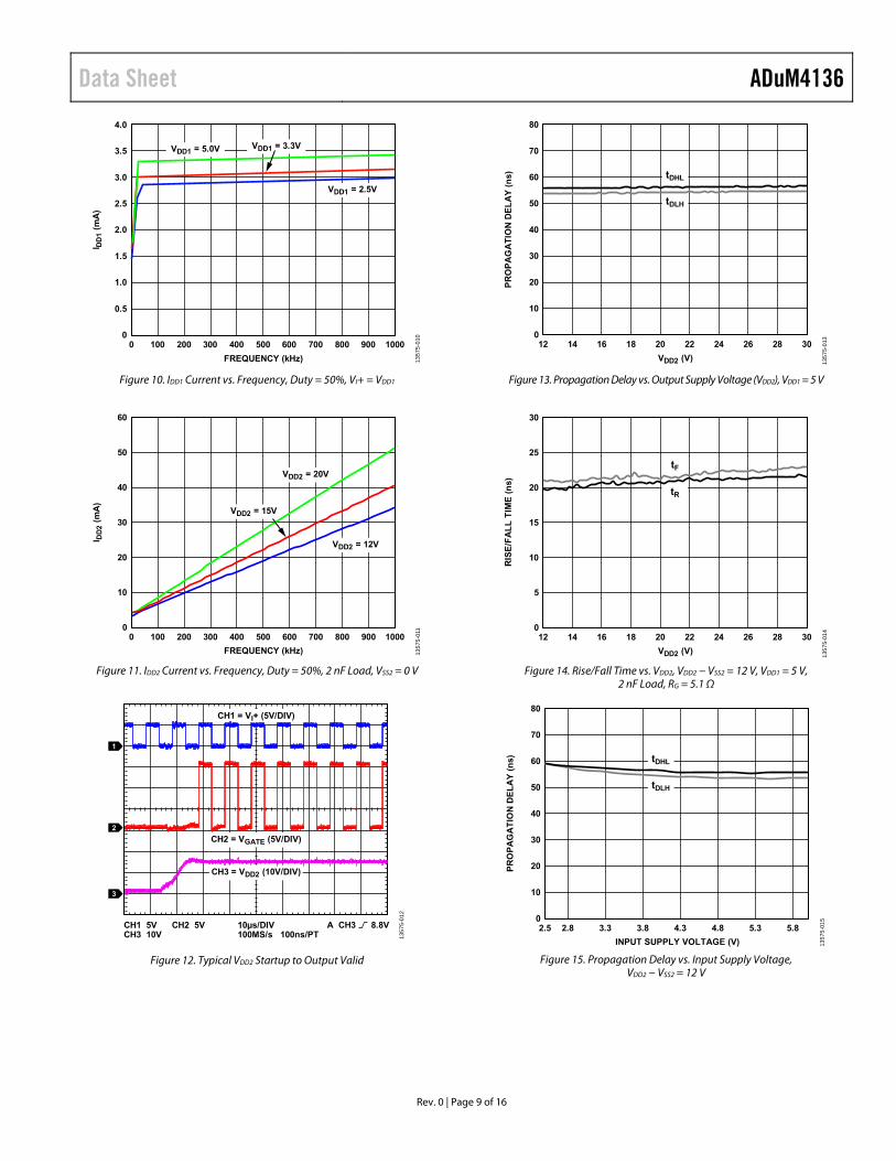
4.0
0
0.5
1.0
1.5
2.0
2.5
3.0
3.5
0 100 200 300 400 500 600 700 800 900 1000
I DD
1 (
mA
)
FREQUENCY (kHz)
VDD1 = 2.5V
VDD1 = 3.3VVDD1 = 5.0V
1357
5-01
0
Figure 10. IDD1 Current vs. Frequency, Duty = 50%, VI+ = VDD1
60
0
10
20
30
40
50
0 100 200 300 400 500 600 700 800 900 1000
I DD
2 (
mA
)
FREQUENCY (kHz)
VDD2 = 12V
VDD2 = 15V
VDD2 = 20V
1357
5-01
1
Figure 11. IDD2 Current vs. Frequency, Duty = 50%, 2 nF Load, VSS2 = 0 V
CH1 5VCH3 10V
CH2 5V 10µs/DIV
CH1 = VI+ (5V/DIV)
CH2 = VGATE (5V/DIV)
CH3 = VDD2 (10V/DIV)
100MS/s 100ns/PTA CH3 8.8V
1
2
3
1357
5-01
2
Figure 12. Typical VDD2 Startup to Output Valid
80
70
60
0
10
20
30
40
50
12 14 16 18 20 22 24 26 28 30
PR
OP
AG
AT
ION
DE
LA
Y (
ns)
VDD2 (V)
tDHL
tDLH
1357
5-01
3
Figure 13. Propagation Delay vs. Output Supply Voltage (VDD2), VDD1 = 5 V
30
0
5
10
15
20
25
12 14 16 18 20 22 24 26 28 30
RIS
E/F
AL
L T
IME
(n
s)
VDD2 (V)
tR
tF
1357
5-01
4
Figure 14. Rise/Fall Time vs. VDD2, VDD2 − VSS2 = 12 V, VDD1 = 5 V, 2 nF Load, RG = 5.1 Ω
80
70
60
0
10
20
30
40
50
2.5 2.8 3.3 3.8 4.3 4.8 5.3 5.8
PR
OP
AG
AT
ION
DE
LA
Y (
ns)
INPUT SUPPLY VOLTAGE (V)
tDHL
tDLH
1357
5-01
5
Figure 15. Propagation Delay vs. Input Supply Voltage, VDD2 − VSS2 = 12 V
ADuM4136 Data Sheet
Rev. 0 | Page 10 of 16
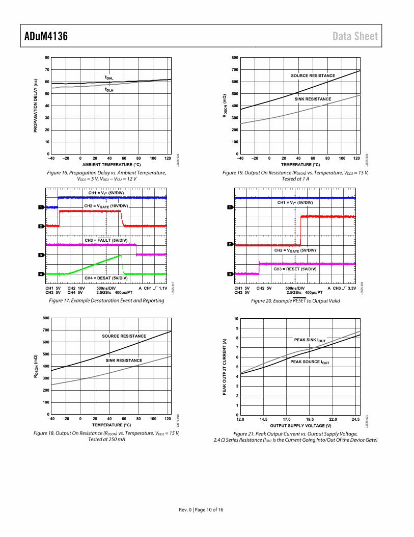
80
70
60
0
10
20
30
40
50
–40 –20 0 20 40 60 80 100 120
PR
OP
AG
AT
ION
DE
LA
Y (
ns)
AMBIENT TEMPERATURE (°C)
tDHL
tDLH
1357
5-01
6Figure 16. Propagation Delay vs. Ambient Temperature,
VDD2 = 5 V, VDD2 − VSS2 = 12 V
CH1 5VCH3 5V
CH2 10VCH4 5V
500ns/DIV
CH1 = VI+ (5V/DIV)
CH2 = VGATE (10V/DIV)
CH3 = FAULT (5V/DIV)
CH4 = DESAT (5V/DIV)
2.5GS/s 400ps/PTA CH1 1.1V
1
2
4
3
1357
5-01
7
Figure 17. Example Desaturation Event and Reporting
800
700
600
0
100
200
300
400
500
–40 –20 0 20 40 60 80 100 120
RD
SO
N (
mΩ
)
TEMPERATURE (°C)
SOURCE RESISTANCE
SINK RESISTANCE
1357
5-01
8
Figure 18. Output On Resistance (RDSON) vs. Temperature, VDD2 = 15 V, Tested at 250 mA
800
700
600
0
100
200
300
400
500
–40 –20 0 20 40 60 80 100 120
RD
SO
N (
mΩ
)
TEMPERATURE (°C)
SOURCE RESISTANCE
SINK RESISTANCE
1357
5-01
9
Figure 19. Output On Resistance (RDSON) vs. Temperature, VDD2 = 15 V, Tested at 1 A
CH1 5VCH3 5V
CH2 5V 500ns/DIV
CH1 = VI+ (5V/DIV)
CH2 = VGATE (5V/DIV)
2.5GS/s 400ps/PTA CH3 3.3V
1
2
3
CH3 = RESET (5V/DIV)
1357
5-02
0
Figure 20. Example RESET to Output Valid
10
9
8
7
6
0
1
2
3
4
5
12.0 14.5 17.0 19.5 22.0 24.5
PE
AK
OU
TP
UT
CU
RR
EN
T (
A)
OUTPUT SUPPLY VOLTAGE (V)
PEAK SINK IOUT
PEAK SOURCE IOUT13
575-
021
Figure 21. Peak Output Current vs. Output Supply Voltage, 2.4 Ω Series Resistance (IOUT is the Current Going Into/Out Of the Device Gate)
Data Sheet ADuM4136
Rev. 0 | Page 11 of 16
APPLICATIONS INFORMATION PCB LAYOUT The ADuM4136 IGBT gate driver requires no external interface circuitry for the logic interfaces. Power supply bypassing is required at the input and output supply pins. Use a small ceramic capacitor with a value between 0.01 μF and 0.1 μF to provide a good high frequency bypass. On the output power supply pin, VDD2, it is recommended to add a 10 μF capacitor to provide the charge required to drive the gate capacitance at the ADuM4136 outputs. On the output supply pin, avoid the use of vias on the bypass capacitor or employ multiple vias to reduce the inductance in the bypassing. The total lead length between both ends of the smaller capacitor and the input or output power supply pin must not exceed 5 mm.
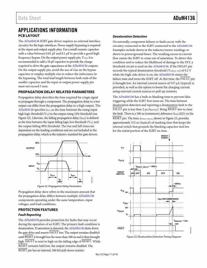
PROPAGATION DELAY RELATED PARAMETERS Propagation delay describes the time required for a logic signal to propagate through a component. The propagation delay to a low output can differ from the propagation delay to a high output. The ADuM4136 specifies tDLH as the time between the rising input high logic threshold (VIH) to the output rising 10% threshold (see Figure 22). Likewise, the falling propagation delay (tDHL) is defined as the time between the input falling logic low threshold (VIL) and the output falling 90% threshold. The rise and fall times are dependent on the loading conditions and are not included in the propagation delay, which is the industry standard for gate drivers.
OUTPUT
INPUT
90%
10%
VIH
VIL
tDLH
tR tF
tDHL
1357
5-02
2
Figure 22. Propagation Delay Parameters
Propagation delay skew refers to the maximum amount that the propagation delay differs between multiple ADuM4136 components operating under the same temperature, input voltages, and load conditions.
PROTECTION FEATURES Fault Reporting
The ADuM4136 provides protection for faults that may occur during the operation of an IGBT. The primary fault condition is desaturation. If saturation is detected, the ADuM4136 shuts down the gate drive and asserts FAULT low. The output remains disabled until RESET is brought low for more than 500 ns and is then brought high. FAULT is reset to high on the falling edge of RESET. While RESET remains held low, the output remains disabled. The RESET pin has an internal, 300 kΩ pull-down resistor.
Desaturation Detection
Occasionally, component failures or faults occur with the circuitry connected to the IGBT connected to the ADuM4136. Examples include shorts in the inductor/motor windings or shorts to power/ground buses. The resulting excess in current flow causes the IGBT to come out of saturation. To detect this condition and to reduce the likelihood of damage to the FET, a threshold circuit is used on the ADuM4136. If the DESAT pin exceeds the typical desaturation threshold (VDESAT, TH) of 9.2 V while the high-side driver is on, the ADuM4136 enters the failure state and turns the IGBT off. At this time, the FAULT pin is brought low. An internal current source of 537 μA (typical) is provided, as well as the option to boost the charging current using external current sources or pull-up resistors.
The ADuM4136 has a built-in blanking time to prevent false triggering while the IGBT first turns on. The time between desaturation detection and reporting a desaturation fault to the FAULT pin is less than 2 μs (tREPORT). Bring RESET low to clear the fault. There is a 500 ns (minimum) debounce (tDEB_RESET) on the RESET pin. The time, tDESAT_DELAY, shown in Figure 23, provides approximately 312 ns (typical) of masking time that keeps the internal switch that grounds the blanking capacitor tied low for the initial portion of the IGBT on time.
VDESAT
VDD2
Vf
9V
FAULT
VCE9V
<200ns
VGATE
DESATSWITCH ONOFF OFF
VI+
DESATEVENT
ONON
~2µs RECOMMENDED
tREPORT < 2µs
tDESAT_DELAY = 300ns
1357
5-02
3
Figure 23. Desaturation Detection Timing Diagram
ADuM4136 Data Sheet
Rev. 0 | Page 12 of 16
For the following design example, see the schematic shown in Figure 29 along with the timing diagrams in Figure 23. Under normal operation, during IGBT off times, the voltage across the IGBT (VCE) rises to the rail voltage supplied to the system. In this case, the blocking diode shuts off, protecting the ADuM4136 from high voltages. During the off times, the internal desaturation switch is on, accepting the current going through the RBLANK resistor, which allows the CBLANK capacitor to remain at a low voltage. For the first 312 ns (typical) of the IGBT on time, the internal desaturation switch remains on, clamping the DESAT pin voltage low.
After the 312 ns (typical) delay time, the DESAT pin is released, and the DESAT pin is allowed to rise towards VDD2 either by the internal current source on the DESAT pin, or additionally with an optional external pull-up resistor, RBLANK, to increase the current drive if it is not clamped by the collector or drain of the switch being driven. RDESAT is chosen to dampen the current at this time, typically selected around 100 Ω to 2 kΩ. Select the blocking diode to block above the high rail voltage on the collector of the IGBT and to be a fast recovery diode.
In the case of a desaturation event, VCE rises above the 9.2 V threshold in the desaturation detection circuit. If no RBLANK resistor is used to increase the blanking current, the voltage on the blanking capacitor, CBLANK, rises at a rate of 537 μA (typical) divided by the CBLANK capacitance. Depending on the IGBT specifications, a blanking time of approximately 2 μs is a typical design choice. When the DESAT pin rises above the 9.2 V threshold, a fault registers, and within 200 ns, the gate output drives low. The output is brought low using the N-FET fault MOSFET, which is approximately 35 times more resistive than the internal gate driver N-FET, to perform a soft shutdown to reduce the chance of an overvoltage spike on the IGBT during an abrupt turn-off event. Within 2 μs, the fault is communicated back to the primary side FAULT pin. To clear the fault, a reset is required.
Thermal Shutdown
If the internal temperature of the ADuM4136 exceeds 155°C (typical), the device enters thermal shutdown (TSD). During the thermal shutdown time, the READY pin is brought low on the primary side, and the gate drive is disabled. When TSD occurs, the device does not leave TSD until the internal temperature drops below 135°C (typical), at which time the READY pin returns to high, and the device exits shutdown.
Undervoltage Lockout (UVLO) Faults
UVLO faults occur when the supply voltages are below the specified UVLO threshold values. During a UVLO event on either the primary side or secondary side, the READY pin goes low, and the gate drive is disabled. When the UVLO condition is removed, the device resumes operation, and the READY pin goes high.
READY Pin
The open-drain READY pin is an output that confirms communi-cation between the primary to secondary sides is active. The
READY pin remains high when there are no UVLO or TSD events present. When the READY pin is low, the IGBT gate is driven low.
Table 11. READY Pin Logic Table UVLO TSD READY Pin Output No No High Yes No Low No Yes Low Yes Yes Low
FAULT Pin
The open-drain FAULT pin is an output to communicate that a desaturation fault has occurred. When the FAULT pin is low, the IGBT gate is driven low. If a desaturation event occurs, the RESET pin must be driven low for at least 500 ns, then high to return operation to the IGBT gate drive.
RESET Pin
The RESET pin has an internal 300 kΩ (typical) pull-down resistor. The RESET pin accepts CMOS level logic. When the RESET pin is held low, after a 500 ns debounce time, any faults on the FAULT pin are cleared. While the RESET pin is held low, the switch on VOUT is closed, bringing the gate voltage of the IGBT low. When RESET is brought high, and no fault exists, the device resumes operation.
RESET
FAULT
<500ns 500ns
1357
5-02
4
Figure 24. RESET Timing
VI+ and VI− Operation
The ADuM4136 has two drive inputs, VI+ and VI−, to control the IGBT gate drive signal, VOUT. Both the VI+ and VI− inputs use CMOS logic level inputs. The input logic of the VI+ and VI− pins can be controlled by either asserting VI+ high or VI− low. With the VI− pin low, the VI+ pin accepts positive logic. If VI+ is held high, the VI− pin accepts negative logic. If a fault is asserted, transmission is blocked until the fault is cleared by the RESET pin.
VI+
FAULT
VI– VOUT
1357
5-02
5
Figure 25. VI+ and VI− Block Diagram
The minimum pulse width is the minimum period in which the timing specifications are guaranteed.
Data Sheet ADuM4136
Rev. 0 | Page 13 of 16
Gate Resistance Selection
It is generally desired to have the turn off occur faster than the turn on. To select the series resistance, decide what the maximum allowed peak current is for the IGBT. Knowing the voltage swing on the gate, as well as the internal resistance of the gate driver, an external resistor can be chosen.
IPEAK = (VDD2 − VSS2)/(RDSON_N + RGOFF)
For example, if the turn-off peak current is 4 A, with a (VDD2 − VSS2) of 18 V,
RGOFF = ((VDD2 − VSS2) − IPEAK × RDSON_N)/IPEAK
RGOFF = (18 V − 4 A × 0.6 Ω)/4 A = 3.9 Ω
After RGOFF is selected, a slightly larger RGON can be selected to arrive at a slower turn-on time.
POWER DISSIPATION During the driving of an IGBT gate, the driver must dissipate power. This power is not insignificant and can lead to TSD if considerations are not made. The gate of an IGBT can be roughly simulated as a capacitive load. Due to Miller capacitance and other nonlinearities, it is common practice to take the stated input capacitance, CISS, of a given IGBT, and multiply it by a factor of 5 to arrive at a conservative estimate to approximate the load being driven. With this value, the estimated total power dissipation in the system due to switching action, PDISS, is given by
PDISS = CEST × (VDD2 − VSS2)2 × fS
where: CEST = CISS × 5. fS is the switching frequency of the IGBT.
This power dissipation is shared between the internal on resistances of the internal gate driver switches and the external gate resistances, RGON and RGOFF. The ratio of the internal gate resistances to the total series resistance allows the calculation of losses seen within the ADuM4136 chip.
PDISS_ADuM4136 = PDISS × 0.5(RDSON_P/(RGON + RDSON_P) + RDSON_N/(RGOFF + RDSON_N))
Taking the power dissipation found inside the chip and multiplying it by the θJA gives the rise above ambient temperature that the ADuM4136 experiences.
TADuM4136 = θJA × PDISS_ADuM4136 + TAMB
For the device to remain within specification, TADUM4136 must not exceed 125°C. If TADuM4136 exceeds 155°C (typical), the device enters thermal shutdown.
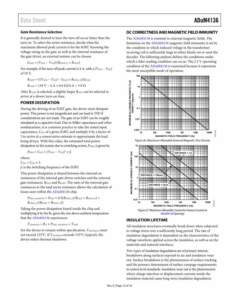
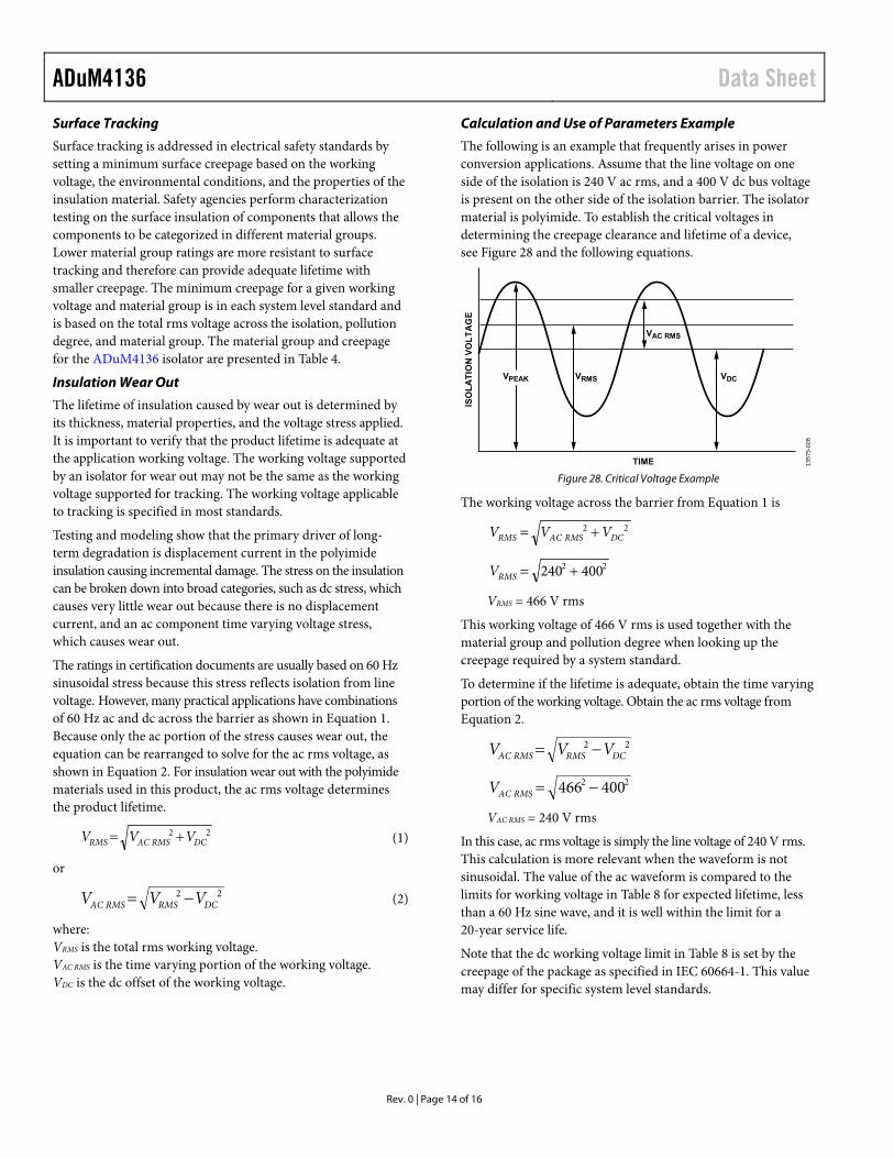
DC CORRECTNESS AND MAGNETIC FIELD IMMUNITY The ADuM4136 is resistant to external magnetic fields. The limitation on the ADuM4136 magnetic field immunity is set by the condition in which induced voltage in the transformer receiving coil is sufficiently large to either falsely set or reset the decoder. The following analysis defines the conditions under which a false reading condition can occur. The 2.5 V operating condition of the ADuM4136 is examined because it represents the most susceptible mode of operation.
100
10
1
0.1
0.01
0.0011k 10k 100k 1M 10M 100M
MA
XIM
UM
AL
LO
WA
BL
E M
AG
NE
TIC
FL
UX
DE
NS
ITY
(kg
auss
)
MAGNETIC FIELD FREQUENCY (Hz) 1357
5-02
6
Figure 26. Maximum Allowable External Magnetic Flux Density
1k
100
10
1
0.1
0.011k 10k 100k 1M 10M 100M
MA
XIM
UM
AL
LO
WA
BL
E C
UR
RE
NT
(kA
)
MAGNETIC FIELD FREQUENCY (Hz)
DISTANCE = 1m
DISTANCE = 100mm
DISTANCE = 5mm
1357
5-02
7
Figure 27. Maximum Allowable Current for Various Current to
ADuM4136 Spacings
INSULATION LIFETIME All insulation structures eventually break down when subjected to voltage stress over a sufficiently long period. The rate of insulation degradation is dependent on the characteristics of the voltage waveform applied across the insulation, as well as on the materials and material interfaces.
Two types of insulation degradation are of primary interest: breakdown along surfaces exposed to air and insulation wear out. Surface breakdown is the phenomenon of surface tracking and the primary determinant of surface creepage requirements in system level standards. Insulation wear out is the phenomenon where charge injection or displacement currents inside the insulation material cause long-term insulation degradation.
ADuM4136 Data Sheet
Rev. 0 | Page 14 of 16
Surface Tracking
Surface tracking is addressed in electrical safety standards by setting a minimum surface creepage based on the working voltage, the environmental conditions, and the properties of the insulation material. Safety agencies perform characterization testing on the surface insulation of components that allows the components to be categorized in different material groups. Lower material group ratings are more resistant to surface tracking and therefore can provide adequate lifetime with smaller creepage. The minimum creepage for a given working voltage and material group is in each system level standard and is based on the total rms voltage across the isolation, pollution degree, and material group. The material group and creepage for the ADuM4136 isolator are presented in Table 4.
Insulation Wear Out
The lifetime of insulation caused by wear out is determined by its thickness, material properties, and the voltage stress applied. It is important to verify that the product lifetime is adequate at the application working voltage. The working voltage supported by an isolator for wear out may not be the same as the working voltage supported for tracking. The working voltage applicable to tracking is specified in most standards.
Testing and modeling show that the primary driver of long-term degradation is displacement current in the polyimide insulation causing incremental damage. The stress on the insulation can be broken down into broad categories, such as dc stress, which causes very little wear out because there is no displacement current, and an ac component time varying voltage stress, which causes wear out.
The ratings in certification documents are usually based on 60 Hz sinusoidal stress because this stress reflects isolation from line voltage. However, many practical applications have combinations of 60 Hz ac and dc across the barrier as shown in Equation 1. Because only the ac portion of the stress causes wear out, the equation can be rearranged to solve for the ac rms voltage, as shown in Equation 2. For insulation wear out with the polyimide materials used in this product, the ac rms voltage determines the product lifetime.
22DCRMSACRMS VVV (1)
or
22DCRMSRMSAC VVV (2)
where: VRMS is the total rms working voltage. VAC RMS is the time varying portion of the working voltage. VDC is the dc offset of the working voltage.
Calculation and Use of Parameters Example
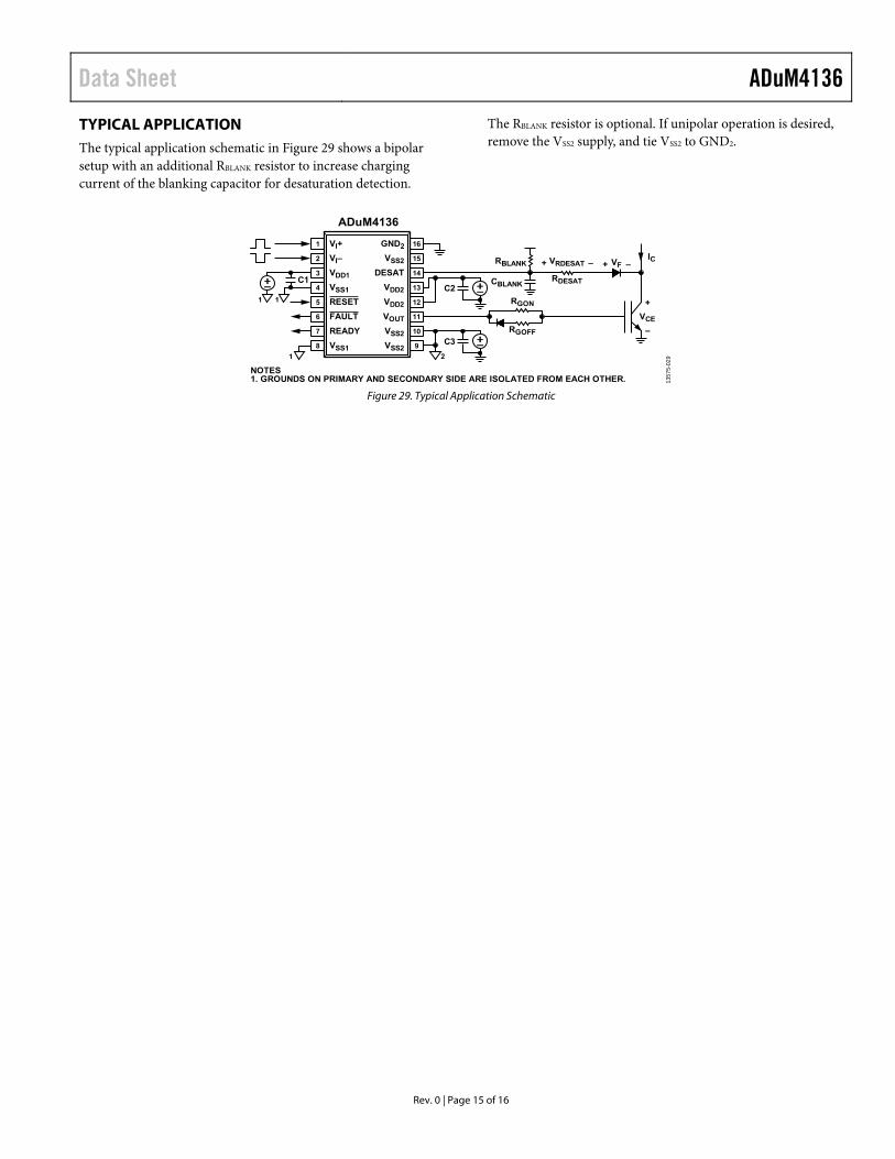
The following is an example that frequently arises in power conversion applications. Assume that the line voltage on one side of the isolation is 240 V ac rms, and a 400 V dc bus voltage is present on the other side of the isolation barrier. The isolator material is polyimide. To establish the critical voltages in determining the creepage clearance and lifetime of a device, see Figure 28 and the following equations.
ISO
LA
TIO
N V
OL
TA
GE
TIME
VAC RMS
VRMS VDCVPEAK
1357
5-02
8
Figure 28. Critical Voltage Example
The working voltage across the barrier from Equation 1 is
22DCRMSACRMS VVV
22 400240 RMSV
VRMS = 466 V rms
This working voltage of 466 V rms is used together with the material group and pollution degree when looking up the creepage required by a system standard.
To determine if the lifetime is adequate, obtain the time varying portion of the working voltage. Obtain the ac rms voltage from Equation 2.
22DCRMSRMSAC VVV
22 400466 RMSACV
VAC RMS = 240 V rms
In this case, ac rms voltage is simply the line voltage of 240 V rms. This calculation is more relevant when the waveform is not sinusoidal. The value of the ac waveform is compared to the limits for working voltage in Table 8 for expected lifetime, less than a 60 Hz sine wave, and it is well within the limit for a 20-year service life.
Note that the dc working voltage limit in Table 8 is set by the creepage of the package as specified in IEC 60664-1. This value may differ for specific system level standards.
Data Sheet ADuM4136
Rev. 0 | Page 15 of 16
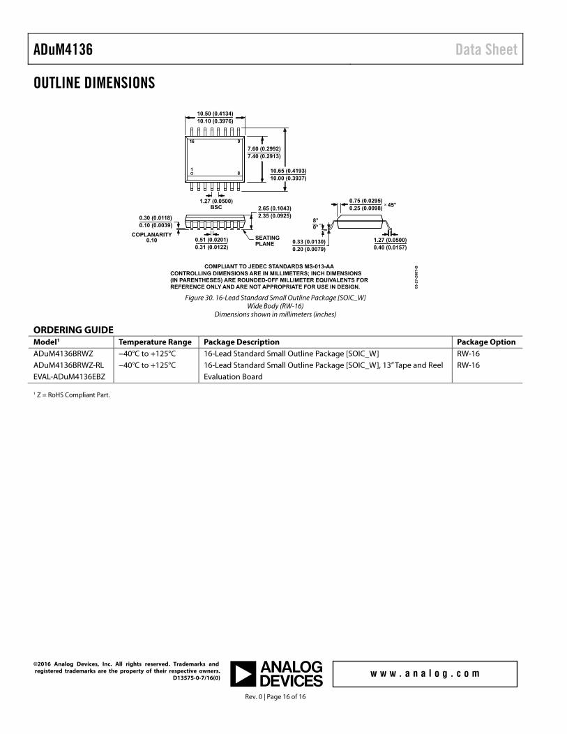
TYPICAL APPLICATION The typical application schematic in Figure 29 shows a bipolar setup with an additional RBLANK resistor to increase charging current of the blanking capacitor for desaturation detection.
The RBLANK resistor is optional. If unipolar operation is desired, remove the VSS2 supply, and tie VSS2 to GND2.
VI+1
VI–2
VDD13
VSS14
GND2 16
VSS2 15
DESAT 14
VDD2 13
RESET5 VDD2 12
FAULT6 VOUT 11
READY7 VSS2 10
VSS18 VSS2 9
ADuM4136
C1
RBLANK
CBLANK
+
VCE
–
IC
C2
C3
RGON
RDESAT
VRDESAT+ – VF –+
RGOFF
NOTES1. GROUNDS ON PRIMARY AND SECONDARY SIDE ARE ISOLATED FROM EACH OTHER. 13
575-
029
1 1
1 2
Figure 29. Typical Application Schematic
ADuM4136 Data Sheet
Rev. 0 | Page 16 of 16
OUTLINE DIMENSIONS
CONTROLLING DIMENSIONS ARE IN MILLIMETERS; INCH DIMENSIONS(IN PARENTHESES) ARE ROUNDED-OFF MILLIMETER EQUIVALENTS FORREFERENCE ONLY AND ARE NOT APPROPRIATE FOR USE IN DESIGN.
COMPLIANT TO JEDEC STANDARDS MS-013-AA
10.50 (0.4134)10.10 (0.3976)
0.30 (0.0118)0.10 (0.0039)
2.65 (0.1043)2.35 (0.0925)
10.65 (0.4193)10.00 (0.3937)
7.60 (0.2992)7.40 (0.2913)
0.75 (0.0295)0.25 (0.0098)
45°
1.27 (0.0500)0.40 (0.0157)
COPLANARITY0.10 0.33 (0.0130)
0.20 (0.0079)
0.51 (0.0201)0.31 (0.0122)
SEATINGPLANE
8°0°
16 9
81
1.27 (0.0500)BSC
03-2
7-2
007
-B
Figure 30. 16-Lead Standard Small Outline Package [SOIC_W] Wide Body (RW-16)
Dimensions shown in millimeters (inches)
ORDERING GUIDE Model1 Temperature Range Package Description Package Option ADuM4136BRWZ −40°C to +125°C 16-Lead Standard Small Outline Package [SOIC_W] RW-16 ADuM4136BRWZ-RL −40°C to +125°C 16-Lead Standard Small Outline Package [SOIC_W], 13” Tape and Reel RW-16 EVAL-ADuM4136EBZ Evaluation Board
1 Z = RoHS Compliant Part.
©2016 Analog Devices, Inc. All rights reserved. Trademarks and registered trademarks are the property of their respective owners.
D13575-0-7/16(0)