single-event-transient effects in sub-70 nm...
TRANSCRIPT
SINGLE-EVENT-TRANSIENT EFFECTS IN SUB-70 NM BULK AND
SOI FINFETS
By
Farah El Mamouni
Dissertation
Submitted to the Faculty of the
Graduate School of Vanderbilt University
in partial fulfillment of the requirements
for the degree of
DOCTOR OF PHILOSOPHY
in
Electrical Engineering
August, 2012
Nashville, Tennessee
Approved:
Ronald D. Schrimpf
Robert A. Reed
Michael L. Alles
Daniel M. Fleetwood
Sokrates Pantelides

ii
Copyright © 2012 by Farah El Mamouni
All Rights Reserved

iii
To
Ahmed El Mamouni

iv
ACKNOWLEDGMENT
I would like to thank the HiREV Program and DTRA’s Basic Research Program for
financially supporting this work.
I would like to thank my advisor, Dr. Ronald D. Schrimpf for being a wonderful pro-
fessor, a good friend, and an outstanding mentor. I thank him for his great contribution to
improving my technical skills as well as assisting my personality to blossom.
I would like to thank Dr. Robert A. Reed, for helping me dive in the sea of single
event effects. His guidance during testing trips and group meetings was priceless.
I would like to thank Dr. Alles and Dr. Fleetwood for their invaluable discussions.
I would like to thank Dr. Dale McMorrow, Dr. Steve Buchner and Dr. Jeffery Warner
for their help and support performing my laser experiments at NRL. I would like to thank
Dr. Gyorgy Vizkelethy for his patience and assistance to successfully accomplish the
heavy ion experiments at SNL.
I would like to thank Dr Kenneth Galloway for helping out getting our first set of sub-
130 nm imec bulk FinFETs. I would like to thank Dimitri Linten and Dr Eddy Simoen
and Dr Cor Claeys for providing us with our second set of sub-70 nm imec bulk and SOI
FinFETs.
I would like to thank Dr. Enxia Zhang for her help preparing my high-speed packag-
es. I thank her and Michael King for performing my heavy ion experiments when needed.
I would like to thank Andrew Sternberg and Nick Pate for helping me with my Python

v
scripts. Finally I thank all of the RER group students and staff for the interesting and fun
discussions we had in the lab.
I would like to thank my first professor, first cheerleader and the first one who
believed in me, my father, Ahmed El Mamouni. I love you dad…
I would like to thank my mother Nabila for her unconditional love, my brother Anass
for setting a terrific example, my sister Fadoua for telling me once “just do it, I am with
you!” my brother Jassim for his endless encouragements, and my beautiful little sister
Hajar for her crazy and genuine love.
I would like to thank my dear husband Nausher Ahmed for his growing love, contin-
uous support and hilarious friendship.
I would like to thank my mother in law Aziza and my sister in law Awatef for their
continuous prayers and emotional support.

vi
TABLE OF CONTENTS
Page
ACKNOWLEDGMENT .................................................................................................... iv
LIST OF FIGURES ........................................................................................................... ix
Chapter
I. INTRODUCTION ............................................................................................... 1
1.1. Thesis objective .................................................................................................... 1 1.2. Introduction ........................................................................................................... 2 1.3. Introduction to non-planar technology .................................................................. 4 1.3.1. Limits of planar technology ............................................................................... 4
1.3.1.1. Short channel effects ............................................................................... 5 1.3.2. Non-planar technology ................................................................................... 7
1.3.2.1. FinFET technology ................................................................................. 7 1.3.2.2. FinFET operation .................................................................................... 8 1.3.2.3. FinFET scaling ...................................................................................... 10
II. BASICS OF SINGLE EVENT EFFECTS ON ELECTRONIC DEVICES
........................................................................................................................... 11
2.1. Single Event Effects (SEEs) ............................................................................... 11 2.1.1. Definition ......................................................................................................... 11
2.1.2. History.......................................................................................................... 12 2.1.3. Charge generation ........................................................................................ 14
2.1.3.1. Ion/semiconductor interactions ............................................................. 14 2.1.3.2. Charge generation ................................................................................. 15 2.1.3.3. Electron-hole recombination ................................................................. 16
2.1.4. Charge collection ......................................................................................... 16
vii
2.1.4.1. Drift collection ...................................................................................... 18 2.1.4.2. Funneling .............................................................................................. 19 2.1.4.3. Diffusion collection .............................................................................. 19 2.1.4.4. Bipolar amplification ............................................................................ 20 2.1.4.5. Shunt collection .................................................................................... 21
2.2. Device response to single event effects (SEEs) .................................................. 22 2.2.1. Single-Event Effects in Planar MOSFETs ................................................... 22
2.2.1.1. Bulk Planar MOSFETs ......................................................................... 22 2.2.1.2. SOI Planar MOSFETs .......................................................................... 25 2.2.1.3. Summary ............................................................................................... 27
2.2.2. Single-Event Effects in FinFETs ................................................................. 28
III. DEVICE AND EXPERIMENTAL DETAILS ................................................. 30
3.1. Measurement techniques ..................................................................................... 30 3.1.1. Laser source, Naval Research Laboratory (NRL) ........................................ 30
3.1.1.1. Single photon absorption (SPA) ........................................................... 30 3.1.1.2. Two photon absorption (TPA) .............................................................. 33
3.1.2. Heavy ion source .......................................................................................... 35 3.1.2.1. IBICC .................................................................................................... 35 3.1.2.2. TRIBICC ............................................................................................... 36 3.1.2.3. High speed packages ............................................................................. 38
3.2. Devices ................................................................................................................ 39
IV. LASER INDUCED CURRENT TRANSIENTS IN SUB-130 nm BULK AND
SOI FINFETS .................................................................................................... 41
4.1. Bulk FinFETs ...................................................................................................... 41 4.1.1. Device and experimental details ..................................................................... 41 4.1.2. Current transients in the drain region ........................................................... 43
4.1.2.1. Charge collection .................................................................................. 45 4.1.2.2. Charge collection mechanisms ............................................................. 46
4.1.3. Current transients in the fins region ............................................................. 47 4.2. Bulk vs. SOI FinFETs ......................................................................................... 50
4.2.1. Device and experimental details .................................................................. 50 4.2.2. Laser induced current transients in bulk and SOI FinFETs ............................ 52 4.2.3. Laser energy dependence of the charge collection ...................................... 53

viii
4.2.4. Laser energy dependence of the FWHMs .................................................... 55 4.2.5. Drain bias dependence of the charge collection .......................................... 56
V. HEAVY-ION-INDUCED CHARGE COLLECTION IN SUB-70 NM BULK
AND SOI FINFETS .......................................................................................... 60
5.1. Device and experimental details ......................................................................... 60 5.2. Charge collection in bulk FinFETs ..................................................................... 61 5.2. Charge collected in SOI FinFETs ....................................................................... 65
5.2.1. IBICC experimental results .......................................................................... 65 5.2.2. TCAD simulation results ............................................................................. 69
5.3. Current transients in bulk FinFETs ..................................................................... 73
VI. CHARGE COLLECTION MECHANISMS IN FINFETS WITH REDUCED
DRAIN REGION AREAS ................................................................................ 75
6.1. Charge collection in FinFETs with saddle contacts ............................................ 76 6.1.1. Bulk FinFETs ............................................................................................... 77
6.1.1.1. Sensitive area of bulk FinFETs with saddle contacts ............................. 77 6.1.1.2. Current transients in bulk FinFETs with saddle contacts ..................... 78
6.1.2. SOI FinFETs ................................................................................................ 80 6.1.2.1. Substrate-bias-dependence of the transient response of SOI FinFETs with saddle contacts .............................................................................................. 80 6.1.2.2. Current transients in SOI FinFETs with saddle contacts ...................... 81
6.2. Transient shunt effect in FinFETs with saddle contacts ........................................ 84 6.2.1. Bulk FinFETs with saddle contacts ............................................................. 84 6.2.2. SOI FinFETs with saddle contacts ............................................................... 87
6.3. Drain bias dependence of the shunt effect in FinFETs with saddle contacts ...... 88 6.3.1. Bulk FinFETs with saddle contacts ............................................................. 88 6.3.2. SOI FinFETs with saddle contacts ............................................................... 90
VII. CONCLUSION ................................................................................................. 93
REFERENCES ................................................................................................................. 96

ix
LIST OF FIGURES
Page
Figure 1: Depletion required at the threshold voltage (VT) in the channel region and the depletion charge provided by drain/source regions in a planar MOSFET transistor [10]. . 5
Figure 2: Physical structure of a FinFET device [12]. ........................................................ 7
Figure 3: Energy band diagram in the fin at the threshold voltage of an n-channel FinFET device. ................................................................................................................................. 9
Figure 4: Shape of a representative single event pulse measured at a struck p-n junction [24]. ................................................................................................................................... 17
Figure 5: Charge collection in the depletion region in a p-n junction [24]. ...................... 18
Figure 6: The figure shows the progress of funneling from the plasma track creation (on the left) to the funnel build up (on the right) [24]. ............................................................ 19
Figure 7: Diagram of a multilayer structure exhibiting shunt effect [24][48]. ................. 21
Figure 8: Drain and source transient currents induced by a 35 MeV Cl ion beam in a 0.25 µm bulk planar NMOS transistor. The transistor is biased in the OFF state (VD =1V) and in the transmission gate configurations [43]. .................................................................... 23
Figure 9: a). Transient drain currents induced by pulsed laser irradiation in a 0.25 µm NMOS transistor. The transistor is OFF biased and the drain voltage is: 1.8 V, 1 V, 0.6 V, 0.2 V. b). Transient drain currents induced by pulsed laser irradiation in a 50 nm bulk NMOS transistors. The transistor is OFF biased with a drain voltage of 1V [50]. .......... 24
Figure 10: Drain current transients induced by a pulsed laser irradiation in a 0.25 µm technology partially depleted SOI transistor. The device is OFF biased. The drain is biased at different voltages: 1.8, 1.0, 0.6 and 0.2 V [50]. This device was processed with a 400 nm BOX thickness and 100 nm silicon film thickness. .......................................... 26
Figure 11: Drain current transients recorded in a 50 nm gate length FD SOI MOSFET irradiated with a pulsed laser energy of 80 pJ [50]. This device is processed with an 11 nm silicon film and 100 nm BOX thickness. .................................................................... 27
Figure 12: Transient drain current induced by a pulsed laser irradiation in a planar FD SOI MOSFET with a gate length of 50 nm and a floating body and in a non-planar

x
FinFET device with a gate length of 60 nm . The silicon film thickness is: 8 nm and 25 in of the FD SOI devices and the non-planar devices, respectively [55]. ............................. 29
Figure 13: Energy band diagram for silicon illustrating the single photon absorption. hν is the energy of the incident photon. ..................................................................................... 31
Figure 14: Absorption coefficient as a function of the wavelength for silicon [58]. ........ 32
Figure 15: Energy band diagram for silicon illustrating the two-photon absorption. ....... 34
Figure 16: Representative diagram of the experimental set up of IBICC technique [62-63]. .................................................................................................................................... 35
Figure 17: Schematic diagram of the experimental setup used to record current transients in bulk and SOI FinFETs. A 20 GHz TDS6124C scope with 50-ohm impedance was used to visualize and record the transients. ............................................................................... 37
Figure 18: Alumina high-speed package (40 GHz). ........................................................ 38
Figure 19: SEM picture of a 10-fins bulk FinFET. The figure shows the fin width (FW) and the gate length (Lg) parameters. The inset shows the cross section of the bulk FinFET corresponding to one fin [12]. ........................................................................................... 42
Figure 20: Physical structure of the FinFET showing the location of the laser spot in the fin and up to 30 µm away from the fin. Inset: SEM picture of the whole bulk FinFET structure including the gate drain and source terminals. Figures are not to scale [12]. .... 44
Figure 21: Representative semi log current transients recorded in the fins (x = 0-µm) and up to 30-µm underneath the drain away from the fins [12]. ............................................. 44
Figure 22: Charge collected (pC) as a function of x-position from the fins (x = 0 µm) to 30 µm toward the drain region (the blue arrows) as illustrated in Fig. 20 for different laser energies [12]. ..................................................................................................................... 45
Figure 23: Full width at half maximum (FWHM) (ns) as a function of the distance x (µm) for two laser energies: 4.68 nJ and 9.4 nJ. At x = 0 µm, the laser is focused in the fins [12]. ................................................................................................................................... 46
Figure 24: (a) Charge collected (pC) as a function of the distance y (µm) traversed by the laser for 3 different laser energies, 0.98-nJ, 4.68-nJ and 8.2-nJ. (b). SEM picture of the fins region, showing distance traversed by the laser across the fins in the y-direction [12]............................................................................................................................................ 48
Figure 25: Current transients captured in the fins at distances: 3 µm and 5 µm (cf. Fig. 22(b)) for laser energy of 0.89 nJ [12]. ............................................................................. 49
Figure 26: Current transients captured in the fins at distances: 3 µm and 5 µm (cf. Fig. 6(b)) for a laser energy of 4.68 nJ [12]. ............................................................................ 50

xi
Figure 27: SEM picture of a single-fin SOI FinFET. The figure shows the fin width (FW) and the gate length (Lg) parameters. The inset shows the cross section of the FD SOI FinFET [66]. ..................................................................................................................... 51
Figure 28: Semi log drain current transients generated by the pulsed laser in both SOI and bulk FinFETs. The laser energy is 22.4 pJ. A voltage of -0.6 V was applied to both samples during irradiation. The full width at half maximum (FWHM) is illustrated for both devices on the figure [66]. ........................................................................................ 53
Figure 29: Semi log curves showing charge collected (C) for bulk (triangles) and SOI (squares) FinFETs as a function of laser energy [66]. ...................................................... 54
Figure 30: Semi log plot showing FWHM as a function of laser energy for bulk (empty squares) and SOI FinFETs (empty triangles) [66]. ........................................................... 56
Figure 31: Rise time in ps for bulk and SOI bulk FinFETs current transients for different drain biases [66]. ............................................................................................................... 57
Figure 32: Schematic diagram of the (2D) cross section of the drain-substrate region in the bulk FinFET [66]. ....................................................................................................... 58
Figure 33: SEM picture of the cross section of bulk FinFET is shown on the right. On the left is illustrated the schematic cross sections [69]. The well doping is ~1017 cm-3. ......... 60
Figure 34: (a) Charge collected in the drain terminal of a bulk FinFET with a 5 nm fin width and a gate length of 70 nm. (b) Projection of the charge-collected values on the (x, y) plan defining the sensitive area of the tested structure [12]. ........................................ 62
Figure 35: (a) SEM picture showing the location of the FinFET device on the die. (b) Top layout view of a FinFET device with 5-fins. All tested devices have the same parameters illustrated on the layout unless otherwise mentioned [12]. ............................................... 62
Figure 36: Projected values of the charge collected (fC) shown in Fig. 2(a) on the x-axis (µm) [12]. .......................................................................................................................... 63
Figure 37: Pictures of the cell layout and an SEM of a FinFET based SRAM cell built in imec [69]. .......................................................................................................................... 64
Figure 38: SEM picture of the cross section of SOI FinFET is shown on the right. On the left is illustrated the schematic cross sections [69]. .......................................................... 65
Figure 39: Values of charge collected (fC) along the x-axis (along the gate) in the substrate (circles) source (triangles) and drain (stars) terminals. The SOI FinFET was biased in the off state configuration with a grounded substrate [73]. ............................... 67
Figure 40: Values of charge collected (fC) along the x-axis (along the gate) in the substrate (circles) source (triangles) and drain (stars) terminals. The SOI FinFET was biased in the off state configuration with a substrate bias of -4V [73]. ............................ 67

xii
Figure 41: Values of the charge collected (fC) along the x-axis (along the gate) in the substrate source and drain terminals. The SOI FinFET was biased in the off state configuration with a substrate bias of +4V [73]. .............................................................. 68
Figure 42: Enlarged view of the schematic cross section of the SOI MOS capacitor simulated using TCAD. .................................................................................................... 69
Figure 43: Cross section of the SOI MOS capacitor with a grounded substrate. The white line in the substrate illustrates the oxide/substrate depletion region. ................................ 70
Figure 44: Cross section of the SOI MOS capacitor with a substrate voltage of -4 V. The white line in the substrate illustrates the oxide/substrate depletion region. ...................... 71
Figure 45: Cross section of the SOI MOS capacitor with a substrate voltage of +4 V. The absence of the white line in the substrate demonstrates the absence of the depletion region. ............................................................................................................................... 71
Figure 46: Current transient collected in the drain terminal of a bulk FinFET biased in the off state with a drain bias of 0.6 V. The FinFET has 5 fins, each fin is 20 nm wide and 70 nm long. ............................................................................................................................ 74
Figure 47: a). Top layout view of FinFETs with common drain contact (dumbbell contact). b) Top layout view of FinFETs with multiple drain contacts (saddle contact). FinFETs with dumbbell and saddle contacts have different number of fins [73]. ............ 75
Figure 48: (x, y) locations of the transient events recorded in a bulk FinFET with saddle contact. .............................................................................................................................. 77
Figure 49: The solid (black) transient curve was recorded in a FinFET (Wf/L=20/70) with dumbbell contacts. The dashed (red) transient was recorded in a FinFET (Wf/L=20/60) with saddle contacts [73]. ................................................................................................. 79
Figure 50: Projected values of charge collected (fC) along the x-axis (along the gate) in the substrate source and drain terminals. The SOI FinFET was biased in the off state configuration with a bias substrate of -5V. ....................................................................... 81
Figure 51: Current transients recorded in bulk and SOI FinFETs with saddle contacts. Both devices have 10 fins; each fin is 20 nm wide and 60 nm long. Both devices were biased in the off state configuration with a drain bias of 1 V. The body of the SOI FinFET was left floating. ................................................................................................................ 82
Figure 52: Simulated drain current transient in an SOI FinFET. A FWHM of 13 ps is obtained. ............................................................................................................................ 83
Figure 53: Current transients recorded in the drain (black), in the source (red), and in the well (blue) of a bulk FinFET with saddle contacts. The FinFET has a gate length of 60 nm, a fin width of 20 nm and 10 fins in parallel. The FinFET was irradiated in the OFF state configuration, with VD = 1 V and all other terminals grounded [73]. ....................... 85
xiii
Figure 54: The figure on the left illustrates the schematic structure (not to scale) of the cut line along the gate-drain axis of the bulk FinFET shown on the right. The 2D figure summarizes the different mechanisms involved in the charge collection process of the tested bulk FinFET [73]. ................................................................................................... 86
Figure 55: Current transients recorded in the drain (black), in the source (red), and in the well (blue) of an SOI FinFET with saddle contacts. The FinFET has a gate length of 60 nm, a fin width of 20 nm and 10 fins in parallel. The FinFET was irradiated in the OFF state configuration, with VD = 2 V and all other terminals grounded [73]. ....................... 87
Figure 56: Current transients recorded in the drain (black), in the source (red), and in the well (blue) of a bulk FinFET with saddle contacts. The FinFET has a gate length of 60 nm, a fin width of 20 nm and 10 fins in parallel. The FinFET was irradiated in the OFF state configuration, with VD = 2 V and all other terminals grounded [73]. ....................... 89
Figure 57: Current transients recorded in the drain (black), in the source (red), and in the well (blue) of an SOI FinFET with saddle contacts. The FinFET has a gate length of 60 nm, a fin width of 20 nm and 10 fins in parallel. The FinFET was irradiated in the OFF state configuration, with VD = 2 V and all other terminals grounded [73]. ....................... 90

1
CHAPTER I
INTRODUCTION
1.1. Thesis objective
After fourteen years of research and investigations by engineers in the university and
industry communities, FinFET devices are finally ready to use in products [1-2]. FinFET
technologies have been demonstrated to outperform planar technologies for high speed,
low power and high performance applications, while maintaining the shrinking trends of
microelectronics (beyond 32 nm) for at least the next two to three technology genera-
tions. These promising findings were enough for leading chip manufacturers like Intel to
announce their plans to mass-produce FinFETs in the near future [3-4]. However, the de-
vice response in extreme environments (i.e., space) is still not well understood. Exploring
the behavior of FinFETs in such environments is also important for the aerospace and
medical industries, where unhardened commercial off the shelf (COTS) electronics are
used.
The objective of this work is to explore the transient electrical behavior of FinFET
devices in both bulk and SOI technologies in radiation-rich environments through laser
and heavy ion testing. A further objective of this work is to contribute to improving the
performance of FinFET devices, in particular in harsh environments. Indeed, the new re-
sults obtained in this work identify the physical regions in the devices that are most sensi-
tive to radiation effects and how they affect the radiation response. The findings will help

2
engineers to design new generations of FinFET devices with higher tolerance to radiation
effects.
1.2. Introduction
Technology scaling enhances the impact of short channel effects on the electrical be-
havior of integrated devices and circuits. As a consequence, the gate control over the
body in MOSFET devices must be increased. FinFET technology is one of the leading
solutions to satisfy the need for excellent control of the gate over the potential in the
body. These structures can be mass produced with minor changes to the fabrication pro-
cesses used for planar technology. Initial radiation effects investigations on FinFETs
were focused on total ionizing dose effects [5-8], which resulted in a number of journal
and conference publications. Single-event effects (SEEs) in FinFETs, however, are not as
well understood. With Intel and other leading manufacturers bringing FinFET technology
to the marketplace, investigating and analyzing SEEs in FinFET devices is quickly be-
coming an important priority. The test structures and state of the art FinFETs investigated
in this work were provided by manufacturers working to refine their product for higher
SEE tolerance, which illustrates the industry’s interest in understanding these effects.
In this work we investigate single-event transient (SET) effects in bulk and SOI Fin-
FETs through topside and backside laser and heavy ion irradiations. SETs are voltage
spikes that can propagate in circuits and may cause a memory cell to flip its state from 0
to 1 or visa versa. Laser testing is an alternative to ion irradiation to reproduce SEEs in
devices and circuits. Later in this chapter, we briefly introduce the FinFET technology
after explaining the limits and constraints of planar technology.
3
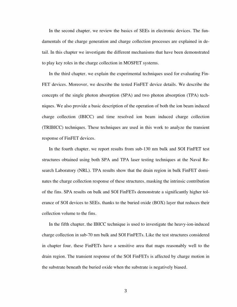
In the second chapter, we review the basics of SEEs in electronic devices. The fun-
damentals of the charge generation and charge collection processes are explained in de-
tail. In this chapter we investigate the different mechanisms that have been demonstrated
to play key roles in the charge collection in MOSFET systems.
In the third chapter, we explain the experimental techniques used for evaluating Fin-
FET devices. Moreover, we describe the tested FinFET device details. We describe the
concepts of the single photon absorption (SPA) and two photon absorption (TPA) tech-
niques. We also provide a basic description of the operation of both the ion beam induced
charge collection (IBICC) and time resolved ion beam induced charge collection
(TRIBICC) techniques. These techniques are used in this work to analyze the transient
response of FinFET devices.
In the fourth chapter, we report results from sub-130 nm bulk and SOI FinFET test
structures obtained using both SPA and TPA laser testing techniques at the Naval Re-
search Laboratory (NRL). TPA results show that the drain region in bulk FinFET domi-
nates the charge collection response of these structures, masking the intrinsic contribution
of the fins. SPA results on bulk and SOI FinFETs demonstrate a significantly higher tol-
erance of SOI devices to SEEs, thanks to the buried oxide (BOX) layer that reduces their
collection volume to the fins.
In the fifth chapter, the IBICC technique is used to investigate the heavy-ion-induced
charge collection in sub-70 nm bulk and SOI FinFETs. Like the test structures considered
in chapter four, these FinFETs have a sensitive area that maps reasonably well to the
drain region. The transient response of the SOI FinFETs is affected by charge motion in
the substrate beneath the buried oxide when the substrate is negatively biased.

4
In the sixth chapter, we investigate the single event response of bulk and SOI Fin-
FETs with reduced (more realistic) drain areas. This study is of crucial significance since
practical bulk FinFETs have similar drain region design. This chapter also illustrates the
impact of this work on today’s FinFET technology. We first compare the transient re-
sponse of FinFETs with conventional drain regions (dumbbell contact) and FinFETs with
reduced drain regions (saddle contact). I explain the different mechanisms contributing to
charge collection and charge enhancement in bulk and SOI FinFETs with saddle contacts.
The bulk vs. SOI comparison demonstrates higher tolerance to SEEs of SOI FinFETs in
comparison to their bulk counterparts.
Finally, I conclude in the seventh chapter by discussing the significance and applica-
tions of this work.
1.3. Introduction to non-planar technology
1.3.1. Limits of planar technology
Intel co-founder Gordon Moore observed that the number of transistors in an integrat-
ed circuit roughly doubles every 2-3 years [9]. This observation has been remarkably ac-
curate over the past five decades. In order to keep pace with Moore’s law, the MOSFETs’
dimensions were reduced by half every 3 years. The channel lengths of the first commer-
cial MOSFETs were greater than 20 µm [10]. Currently, semiconductor manufacturers
are announcing the production of transistors with gate lengths of 20 nm on a regular basis
[3-4]. Transistors with short gate lengths are vulnerable to undesirable short channel ef-
fects [10], which present some of the most important limits to planar MOSFET scaling.
5
1.3.1.1. Short channel effects
Short channel effects refer to modification of ideal electrostatic gate-controlled be-
havior, introducing two-dimensional effects in the channel region. One of the most obvi-
ous manifestations is the threshold voltage reduction when increasing the drain voltage.
This decrease in the threshold voltage is the result of the combined effects of:
source/drain charge sharing, drain-induced barrier lowering (DIBL), and punch-through
[10].
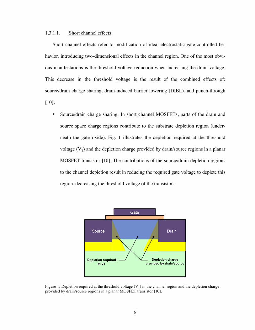
• Source/drain charge sharing: In short channel MOSFETs, parts of the drain and
source space charge regions contribute to the substrate depletion region (under-
neath the gate oxide). Fig. 1 illustrates the depletion required at the threshold
voltage (VT) and the depletion charge provided by drain/source regions in a planar
MOSFET transistor [10]. The contributions of the source/drain depletion regions
to the channel depletion result in reducing the required gate voltage to deplete this
region, decreasing the threshold voltage of the transistor.
Figure 1: Depletion required at the threshold voltage (VT) in the channel region and the depletion charge provided by drain/source regions in a planar MOSFET transistor [10].
6
• Drain induced barrier lowering: Increasing the drain voltage in a short channel
MOSFET can significantly modulate the surface potential in the channel region of
the transistor. Indeed, the surface potential increase in the channel lowers the
source barrier to electron injection into the channel. DIBL reduces the threshold
voltage at high drain biases.
• Punch-through: As in the DIBL case, high drain bias lowers the source-substrate
barrier in a short channel transistor. However, the punch-through conduction takes
place in the silicon bulk. The drain depletion region expands deep in the substrate,
where the doping is low, and reaches the source depletion region, creating a para-
sitic conductive path from source to drain.
The gate oxide thickness is another challenging limit to MOSFET scaling [11]. Tran-
sistors with gate oxides (SiO2) of thicknesses lower than 2 nm are being manufactured. It
has been reported that devices with gate oxides 2 nm thick exhibit leakage current of ~0.1
A/cm2 at 1.2 V [11]. This might not be a threat to general MOSFET applications but it is
considered to be problematic for very low power applications [11]. This result raises con-
cerns when extrapolated to the future.
Several techniques can be adopted to circumvent these scaling limits. However, one
approach that takes care of most of these constraining factors is modifying the physical
structure of MOSFET transistors from planar to 3D technology.
7
1.3.2. Non-planar technology
1.3.2.1. FinFET technology
In an unceasing attempt to increase current drive, control short-channel effects, im-
prove the speed and minimize the power dissipation in devices and circuits, MOS transis-
tors have developed from planar single gate MOS devices into three-dimensional devices
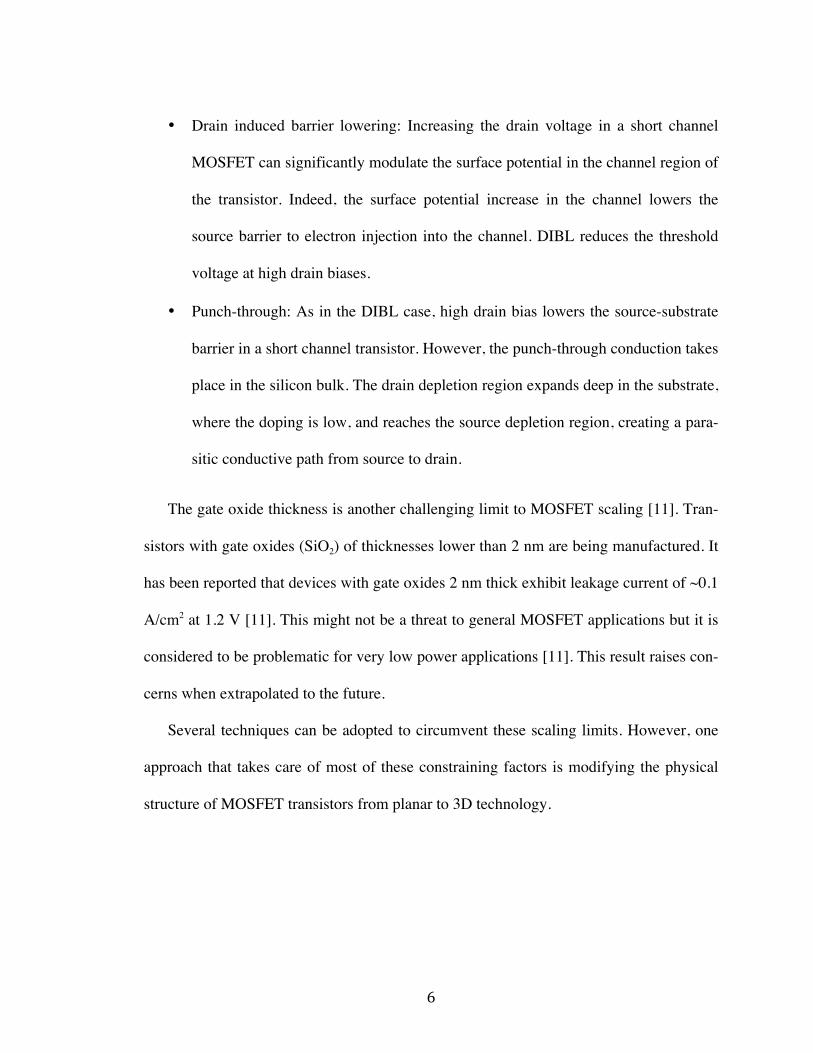
with multiple common gate regions. Fig. 2 illustrates the physical structure of a FinFET
transistor [12].
Figure 2: Physical structure of a FinFET device [12].
Fig. 2 shows that the gate and the poly-silicon wrap around a thin slice of silicon, also
known as a ‘fin’, and the current flows along the top and side surfaces of the fin. The fin’s
dimensions play a key role in defining the operation of the device. Wider fin structures
behave more like planar devices. In narrower fin devices, the additional lateral gates pro-
vide excellent control over the potential in the body by the gates. This significantly miti-

8
gates the short channel effects. Moreover, the lateral gates allow further scaling of the
transistor with a relatively thicker gate oxide in comparison to that of a planar structure.
This reduces the gate tunneling leakage current and improves the drive current of the
FinFET device. Owing to its superior electrostatic scalability and better gate control over
the channel [13], FinFET technology is one of the main candidates to continue CMOS
scaling below the 22-nm node [3]. In fact, Intel Corporation announced in 2011 that the
company is moving to volume production of bulk FinFET-based integrated circuits [14].
Engineers from Intel Corporation announced that an increase in performance of about
37%, versus their own 32 nm planar transistors, could be achieved using bulk FinFET-
based chips, with an increase in process cost of only 2 to 3%. This makes bulk FinFETs
good candidates for volume production, offering a cost advantage over SOI FinFETs,
which require an increase of process cost of almost 10%. The additional fabrication step
where the buried oxide layer (BOX) is added to the SOI wafer increases the process cost
for SOI FinFETs. The BOX layer in SOI FinFETs isolates the fins from the substrate re-
gion.
1.3.2.2. FinFET operation
It is expected that in the future FinFETs may have undoped fins to mitigate random
doping fluctuations, which can produce significant device-to-device variations (i.e., in the
threshold voltage) [15]. The threshold voltage in undoped FinFETs will be controlled by
the gate metal work function. However, until good quality gate metals are available, Fin-
FETs with polysilicon and doped fins are being investigated.
Fig. 3 illustrates the energy band diagram in the fin of an n-channel FinFET biased at
the threshold voltage. A hard mask is usually built on top of the fin to protect it from the

9
different etching steps. This is why the top oxide is usually not used as a gate. FinFETs
with a functional top gate are called tri-gate devices. The process of turning ON a FinFET
device is similar to that of a planar device. However, in FinFET devices both lateral gates
are turned ON, generating current flow along both the gate/silicon surfaces as shown in
Fig. 3.
Figure 3: Energy band diagram in the fin at the threshold voltage of an n-channel FinFET device.
Moreover, thanks to the vertical geometry of FinFETs, their overall gate capacitance
is greater than that of planar devices for the same consumed area and with the same gate
oxide thickness. Equation (1) expresses the threshold voltage of a FinFET device (cf. Fig.
3). The number 2 in the denominator of the third term in the threshold voltage equation
below correspond to the two lateral gates:
(1) VT =VFB + 2!B +QDEP
2COX
10
where VFB is the flat band voltage, ΦB is the silicon bulk potential (kT ln(p/ni)), QDEP is
the depletion (fixed) charge per unit area in the depleted fin, and COX is the oxide capaci-
tance per unit area of one gate.
1.3.2.3. FinFET scaling
In the last decade, CMOS technology experienced striking progress toward scaling of
planar processes. Increasing short channel effects and leakage current formed formidable
obstacles to continue scaling of planar technologies down to 10 nm [16]. Thanks to its
quasi-planar architecture and relatively simple fabrication, research laboratories and in-
dustries have elected FinFET technology as a possible alternative to planar technologies.
Intel is using bulk FinFETs for its 22 nm “Ivy Bridge” processor. Bulk FinFETs have
shown better performance than their planar counterparts. However, bulk FinFET perfor-
mance is still “mid-way” between planar and highly scaled SOI FinFETs. Indeed, due to
their higher junction capacitance and lower mobilities due to the well doping, the present
generation of bulk FinFETs is less likely to outperform SOI FinFETs for applications that
require strong analog performance, for instance [17]. The transient radiation response of
bulk FinFETs is still not well understood. In this thesis, we evaluate the transient re-
sponse of sub-130 nm bulk and SOI FinFETs as well as state of the art bulk FinFETs
with different designs. FinFETs on SOI substrates are examined as well and compared to
their bulk counterparts.
In the next chapter we review the basics of radiation effects on electronic devices, in
particular, single event effects (SEEs).

11
CHAPTER II
BASICS OF SINGLE EVENT EFFECTS ON ELECTRONIC DEVICES
The proper functioning of electronic equipment in radiation-rich environments may
be limited by their vulnerability to single-event effects (SEEs). This can result in errone-
ous data, system shutdown, or even catastrophic failure.
2.1. Single Event Effects (SEEs)
2.1.1. Definition
An electronic system may stop functioning when a heavy ion passes through a sensi-
tive node. This disturbance of the system is called a single-event effect. These effects can
be either destructive or non-destructive. In this thesis we focus on one of the non-
destructive single-event effects, the single event transient (SET). SETs are sudden volt-
age spikes that occur after the passage of a heavy ion through an electronic structure.
These spikes can be propagated in a circuit and cause single event upsets (SEUs). SEUs
occur in memory cells when a state ‘1’ flips to the state ‘0’ or vice versa.

12
2.1.2. History
Single-event upsets were observed in laboratories in the 1970’s [18]. However, the
first data relative to in-flight anomaly was reported by Binder in 1975 [18-19]. Four
events were recorded during periods of low sun activity over 17 years of operational use
of the satellite [19]. It has been demonstrated that cosmic ray interactions can change the
state of digital circuits [19]. Critical transistors in JK flip flop circuits were shown to col-
lect enough charge to turn on and/or off after a cosmic ray passes through a sensitive
node, changing the cell’s state [18-19]. The charge generated by the high-energy cosmic
ray charged the emitter-base capacitance of the critical bipolar transistors in this technol-
ogy to the turn on voltage, modulating the operation of the flip flop circuit and modifying
its state.
SEUs were first discovered in dynamic random access memories (RAMs) and charge
coupled devices (CCDs) in 1978 [20]. d-RAMs store every bit of data in a separate ca-
pacitor where the accumulated charge (~ 1.5 million electrons in 3 µm technology d-
RAM parts [20-21]) is detected by a sensitive amplifier [22]. CCDs are memory devices
where isolated potential wells store charge with typical amounts between 180k and 50k
electrons per bit in 3 µm technology CCD devices [20-21][23]. RAMs and CCDs exhib-
ited the upset of the stored data after the passage of ionizing radiation through the
memory structures [14]. SEUs were caused by alpha particles that emanate from the
packaging material surrounding the electronic structures. Packaging materials like glass
and ceramic contain trace amounts of radioactive elements like Uranium and Thorium
that decay, producing heavily ionizing alpha particles with energies ranging from 3.95
MeV to over 9 MeV [14]. The charge generated by the alpha particles modulates the

13
charge state of the storing nodes, reversing their states and producing upsets, which are
also called soft errors. Unlike hard errors such as those caused by gate oxide break down,
soft errors are not permanent and are easily recovered by outside control [24]. The
amount of charge that differentiates between the 0 and 1 states is called the “critical
charge”. It has been demonstrated that the critical charge is one of the dominant factors in
determining the soft error rate in devices [14].
Very energetic particles (protons, helium and heavy ions with energies of up to 1019
eV [20]) originating from space (cosmic rays, solar wind…) can cross the magnetic field
protecting the earth and reach the atmosphere, where secondary particles (charged or/and
uncharged) may be generated. These particles (photons, electrons, protons, neutrons, mu-
ons and pions [25-26]) can affect electronic systems on the ground. SEUs due to cosmic
rays were first reported on earth in 1979 [20]. Dynamic RAMs and CCD circuits were
found to be sensitive to high-energy cosmic particles at sea level, with the highest soft
fail rates recorded in the CCD devices due to their lower stored charge [20]. A total rate
of ~ 7 soft errors per 106 hours was obtained in the 64k RAM circuit, with 87% of these
events due to the alpha particles. On the other hand, a total rate of ~ 600 soft errors per
106 hours was recorded in the 64k CCD devices. Protons and muons may generate charge
that is higher than the critical charge of the CCDs through direct ionization, resulting in
considerable rates of soft errors in these structures (up to 330 errors per 106 hours) [20]. A
muon is a fundamental or unitary particle like an electron but with a heavier mass (~ 200
me) and a negative charge [27]. Muons are the most ubiquitous charged particles at sea
level [28]. Moreover, CCDs may exhibit significant soft error rates (100 per 106 hours)
due to neutron interactions [20]. Neutrons are uncharged particles that interact with the

14
nucleus, producing electron-hole pairs through heavy nucleus recoils [20]. The next para-
graph will summarize the ion-semiconductor interactions as a function of their mecha-
nisms.
2.1.3. Charge generation
2.1.3.1. Ion/semiconductor interactions
The passage of an energetic particle through a semiconductor material creates elec-
tron-hole pairs. The electron-hole pairs are generated via different mechanisms.
• Rutherford or Coulomb scattering relies upon electronic forces. The incident
charged particle (protons, ions, or electrons) interacts with free (in the conduction
band) and bound electrons in the lattice, producing electron-hole pairs through
Coulomb attraction and/or repulsion. Incident protons with energies lower than
100 keV ionize the target atoms, producing free carriers along its track.
• When the incident particles are more energetic (protons, neutrons, and electrons
with energies higher than 10 MeV [29], 6 MeV [30] and 150 keV [31] respective-
ly), ion-nuclei interactions dominate. Energetic protons and neutrons are more
likely to interact with an atomic nucleus since its volume is 8000 times that of an
electron. An elastic collision can displace an atom from its original position in the
lattice. The recoiled atom acts as a heavy ion in the lattice, producing electron-
hole pairs along its track through ionization. The relocated atom’s vacancy modi-
fies the local lattice potential, generating displacement damage [31]. The energy
received by the displaced atom can also be transferred to the lattice in the form of
phonons (heat).

15
• Spallation is an inelastic nuclear reaction that takes place when a high-energy (≥
50 MeV) incident particle (proton, neutron…) interacts with the nucleus of the
target atom [32]. The spallation reaction is inelastic since the incident particle los-
es some of its energy to the collision. The incident particle’s energy needs to ex-
ceed the interaction energy of the nucleons in the atomic nucleus target so that the
fragmentation of this later is possible [32]. The nucleus ejects secondary particles
that ionize neighboring atoms, producing electron-hole pairs.
2.1.3.2. Charge generation
In general, the incident particle loses energy through Coulomb scattering. The rate of
the transferred energy to the material is often called linear energy transfer (LET) [24]:
where ρ is the material density. Knowing the density of the target material, the amount of
charge created along the path is calculated using the equation above when the LET is
constant. The incident particle eventually loses all of its energy to the target material
when the material thickness is larger than the penetration depth of the incident ion. The
energy loss per distance is maximal at the Bragg peak [33]. This characteristic is often
used in medicine to locate the exact position in the body that will receive the maximum
amount of deposited energy for disease treatments. The distance travelled by the incident
ion is called the range of the ion. It depends on the energy, the atomic number of the ion,
and the nature of the target material.
(1)
16
2.1.3.3. Electron-hole recombination
An important mechanism takes place right after the carriers’ generation process: elec-
tron-hole recombination, which is also called “initial recombination” at these short times
[34]. Models for two limiting cases have analytically quantified the recombination pro-
cess: when the electron/hole pairs are close together (columnar model [35]) and when
they are far apart (geminate model [36]). The distance distinguishing between the two
cases is the thermalization radius. This distance corresponds to the space between an
electron-hole pair after generation once this pair reaches thermal equilibrium [37][38]. In
the columnar model, charge is distributed along the incident ion’s path, forming a column
or a cylinder. This charge is highly dense, so that recombination between electrons and
holes inside the column is possible [34]. On the other hand, the distance separating the
generated electron-hole pair in the geminate model is larger than the thermalization dis-
tance in silicon. Recombination between the generated electron and hole of the same pair
dominates [34] [38]. Recombination rate in the geminate model is much smaller than that
in the columnar model. The charge profile along the incident ion’s track defines the most
convenient recombination model to be used. The charge profile depends on the nature
and the energy of the incident particle [38].
2.1.4. Charge collection
Most of the generated electron-hole pairs in a bulk semiconductor region tend to re-
combine in the absence of an electric field [24-38]. However, when this charge is depos-
ited in or in the neighborhood of a p-n junction, the charge is collected in the depletion
region of the p-n junction, producing a measurable transient photocurrent [24]. The

17
charge collection in IC junctions takes place via several mechanisms that will be ex-
plained in detail in the following paragraphs.
Fig. 4 shows a typical time-dependent current at a struck p-n junction. The integral of
the illustrated pulse represents the charge collected (Qcoll) in the junction. The figure
shows that the rise and the fall times are controlled by different charge collection mecha-
nisms. The drift and the funnel mechanisms govern the fast component of the illustrated
transient, which lasts up to a few hundred picoseconds. The drift and funnel mechanisms
are explained in more detail in the next sections. The slow component or the tail of the
transient is a result of the carriers collected from outside the depletion region of the p-n
junction (via diffusion).
Figure 4: Shape of a representative single event pulse measured at a struck p-n junction [24].
Fig. 4 summarizes the basic mechanisms governing charge collection in a p-n junc-
tion. However, additional processes affect the charge collection, depending on the type of
the device and the nature of the incident particle. For instance, the parasitic bipolar npn
18
(or pnp) structure in SOI technologies, which has been demonstrated to play a key role in
enhancing the collected charge in these structures, is explained later in this section [39].
2.1.4.1. Drift collection
In the presence of an electric field E, the generated electrons and holes due to the in-
cident particle move in opposite directions.
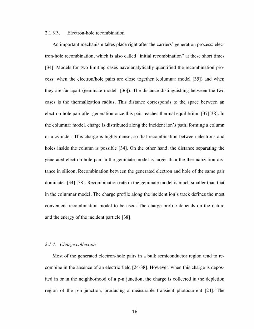
Figure 5: Charge collection in the depletion region in a p-n junction [24].
Fig. 5 shows the depletion region in a reverse-biased p-n junction after the passage of
an ion. Electrons move toward the n-type region (positively biased) and holes proceed to
the p-type region (negatively biased). The charge flow leads to photocurrent generation
or a current pulse that can be measured at the diode terminals. Since the carrier’s motion
is controlled by an electric field, this mechanism is called drift collection.

19
2.1.4.2. Funneling
The generated carrier track can distort the original depletion region in a reverse bi-
ased p-n junction [24] [40-41]. In fact, the created carrier track can temporarily screen the
depletion region. This stretches the resistance along the track, extending the voltage drop
outside the original depletion region as shown in Fig. 6. This results in carrier collection
outside the depletion region, which increases the amount of collected charge in the p-n
diode.
Figure 6: The figure shows the progress of funneling from the plasma track creation (on the left) to the fun-nel build up (on the right) [24].
While drift collection takes a few picoseconds, the funneling process takes a few hundred
picoseconds to proceed [24].
2.1.4.3. Diffusion collection
Carriers that are generated in the substrate, close to the depletion region or the funnel
(distorted depletion region), can diffuse and get collected in the biased (positively or neg-
atively) region of the p-n junction. The current that results from this process occurs at a
later time compared to the field-assisted collection process discussed above. In general,

20
the contribution of diffusion to the charge collection process is observed as a tail in the
current pulse. This tail can extend over a few nanoseconds [24]. In the late seventies
(1979) charge diffusion was assumed to be the dominant soft failure mechanism in devic-
es [42].
2.1.4.4. Bipolar amplification
Bipolar amplification is an inherent characteristic of SOI devices [43]. It is also a di-
rect consequence of the floating body effects in SOI structures. The parasitic npn transis-
tor in an n-channel partially depleted SOI MOSFET (or pnp transistor in a p-channel PD
SOI MOSFET) can turn on after the passage of a heavy ion [39][44-45]. While the gener-
ated minority electrons quickly leave the body [39], the majority carriers (holes) are con-
fined in the body [39]. The holes that escape recombination in the body of an n-channel
SOI device forward bias the source/body junction, triggering the injection of electrons
from the source to the body, where they are collected by the drain terminal. This is called
the bipolar mechanism. This effect can drastically amplify the collected charge, dominat-
ing the SEE response of partially-depleted SOI technologies [39][46]. Fully depleted SOI
technologies have been demonstrated to be vulnerable to bipolar amplification as well
[47]. However the charge amplification in these latter technologies is less significant than
that in their partially-depleted counterparts [47] thanks to their mitigated floating-body
effects assured by the higher control of the gate over the potential in the body. The bipo-
lar phenomenon is mitigated in highly-doped silicon films, which decreases the lifetime
and the mobility of carriers in the silicon. Bulk devices have been demonstrated to be
subject to bipolar amplification as well [43]. This amplification effect is enhanced for
low-doped substrate bulk devices.

21
2.1.4.5. Shunt collection
Plotted in Fig. 7 is a schematic diagram of a multilayer structure exhibiting a distinc-
tive phenomenon that is becoming critically important for modern dense integrated de-
vices [24]. The ion track in Fig. 7 is penetrating two proximate junctions. Thanks to its
high carrier density, the ion track plasma can form a conductive path between the two n
regions in Fig. 7. The conductive path acts as a wire carrying charge that was generated
due to the heavy ion and additional charge that may originate outside the npn structure as
well [24]. This collection mechanism is called the “shunt” effect [24][48-49].
Figure 7: Diagram of a multilayer structure exhibiting shunt effect [24][48].
The results presented in this thesis demonstrate that shunt collection plays a key role
in explaining the charge collection mechanism in bulk and SOI FinFETs.

22
2.2. Device response to single event effects (SEEs)
The critical dimensions of MOS field effect transistors have dramatically decreased
since the 70’s [50]. The transistor’s gate length has dropped from 10 µm in the 1970’s
[50] to 22 nm [3-4] for current technologies. The decrease of device dimensions enhances
the IC’s vulnerability to single-event effects. In the first part of this section, we review
SEEs on planar bulk and SOI MOSFETs. The second part reviews the published data re-
lated to SEEs on FinFETs.
2.2.1. Single-Event Effects in Planar MOSFETs
2.2.1.1. Bulk Planar MOSFETs
Illustrated in Fig. 8 are the recorded current transients in the drain and the source ter-
minals of a bulk planar transistor fabricated in 0.25 µm technology irradiated with a 35
MeV Cl ion beam. The sample is biased in either the off state (VD = 1 V) or the transmis-
sion gate bias (VD = VS = 1 V) configuration. The shape of the drain transient in Fig. 8 is
comparable to that shown in Fig. 4, with two main charge collection mechanisms: drift
collection and diffusion collection.
23
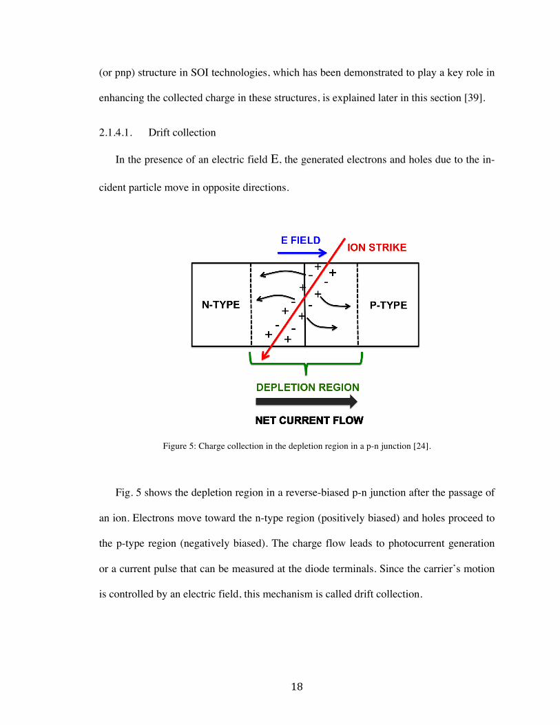
Figure 8: Drain and source transient currents induced by a 35 MeV Cl ion beam in a 0.25 µm bulk planar NMOS transistor. The transistor is biased in the OFF state (VD =1V) and in the transmission gate configu-rations [43].
The drain transients in Fig. 8 exhibit long tails (~ 4 ns), highlighting the diffusion
phenomenon of carriers from the substrate, which dominates the charge collection pro-
cess in these bulk planar devices. Fig. 8 shows that the bulk samples exhibit negative cur-
rent transients in the source terminal for both OFF state and transmission gate bias con-
figurations, with the largest transients obtained for the OFF state configuration. This sug-
gests a conduction path between the drain and the source terminals [43]. Charge collec-
tion in bulk devices may be affected by minor bipolar amplification in low-doped sub-
strate bulk structures. After the passage of a heavy ion through the sample, the source-
substrate junction is forward biased due to the extra holes in the body. Electrons are in-
jected from the source to the body and are collected by the drain due to the positive drain
voltage. The bipolar amplification [43] is more significant in the off-state bias configura-
tion as illustrated in Fig. 8, where the largest negative source transients are obtained. The

24
bipolar effect is less significant in the TG bias configuration since the source, like the
drain, is collecting electrons due to the applied positive bias (VS = 1 V).
Figure 9: a). Transient drain currents induced by pulsed laser irradiation in a 0.25 µm NMOS transistor. The transistor is OFF biased and the drain voltage is: 1.8 V, 1 V, 0.6 V, 0.2 V. b). Transient drain currents induced by pulsed laser irradiation in a 50 nm bulk NMOS transistors. The transistor is OFF biased with a drain voltage of 1V [50].
Illustrated in Fig. 9 are the drain current transients recorded in irradiated 0.25 µm and
50 nm bulk NMOS transistors. Both samples were irradiated with comparable laser ener-
gies (32 pJ and 38 pJ). In contrary to large bulk NMOSFETs, current transients recorded
in smaller devices have smaller pulse amplitudes, widths, and tails [50]. It has been
shown that scaled devices can be more prone to bipolar amplification than their large (1
µm) counterparts [43]. However, the sophisticated doping profiles used in some of the
newer technologies appear to reduce this amplification effect significantly [50]. Moreo-
ver, the heavy well doping of the scaled devices results in less diffusion collection, as
shown in Fig. 9, due to the reduced lifetime of the generated carriers. On the other hand,
higher rates of single and multiple bit upsets were observed in some highly integrated
technologies, which suggests a need to review the diffusion contribution to charge collec-

25
tion in highly scaled technologies [51-52]. In fact, higher doping profiles induce more
complex charge diffusion mechanisms with respect to proximate sensitive regions [51-
52].
2.2.1.2. SOI Planar MOSFETs
In an SOI MOSFET, the thickness of the silicon film determines the physics of the
device operation. When the silicon film thickness (tsi) in the channel is larger than the
maximum depletion width (xdmax), where xdmax is expressed by equation (2), the device is
considered to be partially-depleted (PD) [53].
!!"#$ = !!!"!!!!!
, (2)
where εsi is the silicon permittivity, φF is the Fermi potential or silicon bulk potential, Na
is the silicon film doping per unit volume and q is the elementary charge [53].
On the other hand, When tsi is lower than xdmax, the silicon film is completely depleted and
the device is considered to be fully depleted (FD). The fully-depleted technology miti-
gates the floating body effects usually observed in partially-depleted SOI technologies.
The buried oxide in SOI transistors isolates the active region of the device from the
substrate, reducing the collection volume. This significantly decreases SOI devices’ sen-
sitivity to single event effects in comparison to their bulk counterparts. Illustrated in Fig.
10 are current transients recorded in PD SOI MOSFETs fabricated in a 0.25 µm technol-
ogy.

26
Figure 10: Drain current transients induced by a pulsed laser irradiation in a 0.25 µm technology partially depleted SOI transistor. The device is OFF biased. The drain is biased at different voltages: 1.8, 1.0, 0.6 and 0.2 V [50]. This device was processed with a 400 nm BOX thickness and 100 nm silicon film thick-ness.
The current transients in Fig. 10 exhibit significantly shorter tails than the ones ob-
served in bulk NMOSFETs with the same gate length, as shown in Fig. 9a. This results in
notably smaller amounts of charge collected in SOI devices than their bulk counterparts.
Fig. 11 illustrates the current transients obtained in a FD SOI device with a 50 nm
gate length and 11 nm silicon film thickness [50]. The current transient is very short, with
a FWHM of 35 ps and a width of only 66 ps. The absence of the tail in the 50 nm FD SOI
device confirms the minimal contribution of floating body effects previously observed in
partially depleted device (cf. Fig. 10). The small dimensions of this device reduce the to-
tal collected charge (~ 200 fC) in comparison to bulk devices.

27
Figure 11: Drain current transients recorded in a 50 nm gate length FD SOI MOSFET irradiated with a pulsed laser energy of 80 pJ [50]. This device is processed with an 11 nm silicon film and 100 nm BOX thickness.
It is noteworthy that partially-depleted SOI MOSFETs with gate lengths of 50 nm
have been shown to collect greater amounts of charge than similar devices with 0.25 µm
gate lengths [50] due to bipolar amplification, enhanced by floating body effects. It has
been reported that OFF biased partially depleted SOI NMOSFETs can collect as much as
40 times more charge than that deposited by the incident ion [43].
2.2.1.3. Summary
Bulk planar devices are more sensitive to SEEs than their SOI counterparts due to
their bigger collection volume. Diffusion-related charge collection in bulk planar devices
results in long tails in the transients. The high doping in the wells of scaled planar bulk
devices significantly reduces the amount of collected charge. Smaller transients with
short tails are recorded in SOI devices. Scaled FD SOI devices are less sensitive to SEEs
than their bulk counterparts, with no diffusion signatures in the transients, thanks to their
28
small collection volumes. Partially depleted SOI NMOSFETs can be very sensitive to
bipolar effects when the doping is not optimized.
2.2.2. Single-Event Effects in FinFETs
FinFET technology is relatively new. A fair amount of work related to total ionizing
dose (TID) effects on FinFETs devices has been done. SOI FinFETs with wide fin widths
behave like planar devices [6]. The vertical coupling between the front and the back gates
overpowers the lateral gate coupling [5]. Wide fin devices can be very vulnerable to the
effects of trapped charge in the BOX [5], which can induce effects that are very similar to
those usually observed in planar SOI devices like the “high state current” phenomenon
[5][54]. On the other hand, narrow fin SOI devices have shown higher tolerance to TID
effects thanks to their excellent control of the lateral gate over the electrostatic potential
in the body [5-7]. The isolation oxide in bulk FinFETs appears to significantly affect the
TID response of some narrow fin bulk FinFETs [8]. The trapped charge in the shallow
trench isolation (STI) oxides modulates the potential in the body, making narrow-fin Fin-
FETs more sensitive to total dose effects [8]. Very limited work related to the transient
response of FinFET devices has been reported.
Plotted in Fig. 12 are drain current transients in a planar FD SOI MOSFET (black
curve) and in a non-planar SOI FinFET device (red curve). The planar FD SOI device has
a gate length of 50 nm and a silicon thickness of 8 nm [55]. The gamma shaped SOI Fin-
FET has a gate length of 60 nm, a fin width of 50 nm and a 25 nm tall fin [55]. The BOX
layer in both technologies is 100 nm. In contrast to the fast transients recorded in the pla-

29
nar FD SOI devices, slower transients with longer tails are obtained in the FinFET [55].
This results in greater amount of collected charge in the FinFET.
Figure 12: Transient drain current induced by a pulsed laser irradiation in a planar FD SOI MOSFET with a gate length of 50 nm and a floating body and in a non-planar FinFET device with a gate length of 60 nm . The silicon film thickness is: 8 nm and 25 in of the FD SOI devices and the non-planar devices, respective-ly [55].
It has been demonstrated that the obtained transient response is not intrinsic to the Fin-
FET geometry, but is due to characteristics of these samples [55]. The drain-to-body ac-
cess length in the FinFETs induces the slow shape of the obtained transients [55]. The
generated carriers in the body take more time to reach the drain terminal in the FinFETs,
resulting in the long tails. In fact, with the same values of drain-to-body access distance,
the transients obtained in the FinFETs and the FD SOI devices are very similar [55]. Fin-
FETs used in previous work were test structures fabricated in technologies that are in the
process of being improved in order to reach the level of development of planar FD tech-
nologies. New results of the transient response of state-of-the-art bulk and SOI FinFETs
are presented and investigated in detail in this thesis.
30
CHAPTER III
DEVICE AND EXPERIMENTAL DETAILS
In order to study the SEE response of electronic devices, samples are irradiated in
several accelerator facilities equipped with different beams. Depending on the structure
and on the sensitivity of the studied structure, samples are evaluated using ion and laser
beams with different energies. These testing facilities allow device behavior in space to
be predicted in reduced times compared to actual applications. In this chapter we present
the details of the testing facilities and the measurement techniques, along with the details
about the FinFETs used in this work.
3.1. Measurement techniques
3.1.1. Laser source, Naval Research Laboratory (NRL)
Laser testing is frequently used as a surrogate test for ion irradiation to simulate sin-
gle event effects (SEEs) in microelectronic devices. Laser testing provides the spatial in-
formation and the temporal details of the charge collected, which are necessary to identi-
fy the sensitive nodes and the mechanisms involved in charge collection [56]. Moreover,
laser facilities are less expensive and easy to access in comparison to their ion beam
counterparts. This makes laser testing a good approach for SEE investigation.
3.1.1.1. Single photon absorption (SPA)
The single-photon absorption (SPA) pulsed laser technique originates from the optical
above band gap excitation of carriers in a semiconductor material.

31
Figure 13: Energy band diagram for silicon illustrating the single photon absorption. hν is the energy of the incident photon.
Fig. 13 shows the process of exciting an electron from the valence band into the con-
duction band in silicon. For example, a 1.97 eV photon excites an electron, which jumps
to the conduction band leaving a hole behind in the valence band [55]. The energy of 1.97
eV corresponds to the wavelength of 630 nm used at NRL. The energy is calculated from
the equation:
E = !"! , (3)
where h is Planck’s constant, λ is the photon wavelength (630 nm at NRL) and c is the
speed of light (3 × 10⁸ m.s-1) [57].
The SPA technique injects a well-known amount of charge in a precise location (x, y)
at a specific time. Each photon is absorbed to create an electron-hole pair, hence the sin-
32
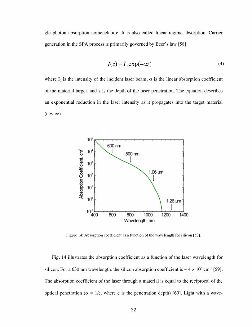
gle photon absorption nomenclature. It is also called linear regime absorption. Carrier
generation in the SPA process is primarily governed by Beer’s law [58]:
where I0 is the intensity of the incident laser beam, α is the linear absorption coefficient
of the material target, and z is the depth of the laser penetration. The equation describes
an exponential reduction in the laser intensity as it propagates into the target material
(device).
Figure 14: Absorption coefficient as a function of the wavelength for silicon [58].
Fig. 14 illustrates the absorption coefficient as a function of the laser wavelength for
silicon. For a 630 nm wavelength, the silicon absorption coefficient is ~ 4 × 103 cm-1 [59].
The absorption coefficient of the laser through a material is equal to the reciprocal of the
optical penetration (α = 1/e, where e is the penetration depth) [60]. Light with a wave-
(4)

33
length of 630 nm can penetrate a distance of ~ 3 µm in the silicon. The penetration depth
value can be varied (up to 10 µm ranges have been successfully achieved in silicon [58])
by choosing the wavelength of the laser. The SPA laser beam is typically focused at the
surface of the device under test.
Also, in contrast to ions, optical pulses cannot pass through metal layers. This can be
a limit to laser techniques for SEE applications, since the amount of generated charge is
directly related to the amount of incident light. The metal layers on top of the sensitive
nodes can modulate the amount of charge collected by the device. The topside SPA tech-
nique is useful for structures that are not covered by metal. However regions with metal
overlayers, in particular advanced structures with multiple metal layers, can still be inves-
tigated using the back side two photon absorption technique as explained in the next par-
agraph.
3.1.1.2. Two photon absorption (TPA)
The light propagates in the material according to the equation [58]:
where I(z) is the laser intensity propagating in the material, α is the absorption coeffi-
cient (single photon), and β is the two photon absorption coefficient (cm-s/Joule). The
equation describes two distinct regimes of absorption, first: linear for single photon ab-
sorption, and second: non linear for two-photon absorption. Working in the non-linear
photon absorption regime requires α to be small (corresponding to wavelengths longer
than 1.2 µm according to Fig. 14). Wavelengths in this range are in the infrared range. IR
wavelengths (0.7 µm to 300 µm) are longer than those of visible light (390 nm to 750
(5)

34
nm), and shorter than those of microwave radiations (1 mm to 1 m). A wavelength of 1.2
µm corresponds to 1 eV photons. Energies below the Si band gap are used, which ex-
plains the need for two photons to generate one electron-hole pair, hence the nomencla-
ture of two photon absorption (TPA).
Figure 15: Energy band diagram for silicon illustrating the two-photon absorption.
Fig. 15 illustrates the two-photon absorption mechanism for a particular laser wave-
length. Two photons, each having a wavelength of 1260 nm excite an electron from the
valence band into the conduction band. An electron-hole pair is created when two pho-
tons are absorbed at the same time by an electron, which is more likely to occur with
higher laser intensities. The carrier generation equation below (6) highlights the intensity
influence on the two-photon absorption process [58]:
where N(z) is the density of free carriers, h is Planck’s constant, ν is the photon frequen-
(6)

35
cy (c/λ). The factor 2 in the non-linear term takes into consideration the generation of one
electron-hole pair for two photons absorbed.
In the next section we explain the heavy ion testing techniques used in this work.
3.1.2. Heavy ion source
Ion beam induced charge collection (IBICC) and transient ion beam induced charge
collection (TRIBICC) techniques are used routinely to study single event effects (SEEs)
in devices and circuits [61].
3.1.2.1. IBICC
Illustrated in Fig. 16 is a representative diagram of the experimental set up of the
IBICC technique [62-63].
Figure 16: Representative diagram of the experimental set up of IBICC technique [62-63].
In contrast to ionizing radiation sensors and other scintillation detectors, the charge
generated in an irradiated semiconductor device is very small [62]. The preamplifier
36
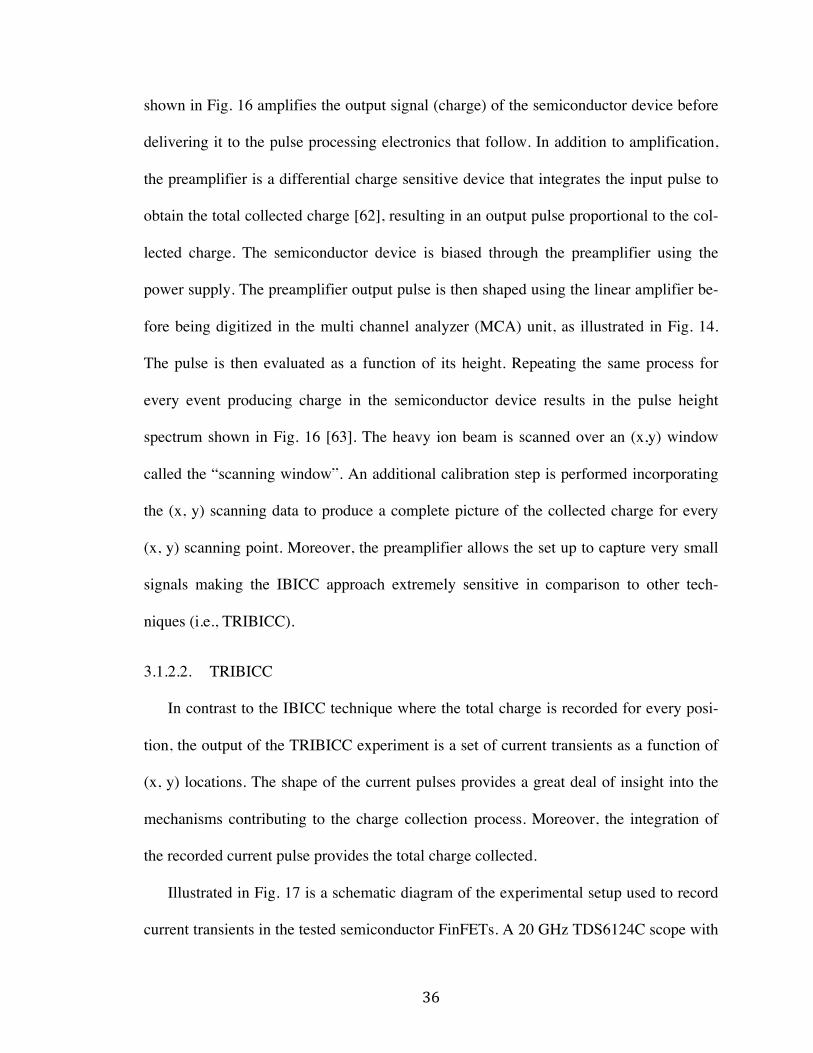
shown in Fig. 16 amplifies the output signal (charge) of the semiconductor device before
delivering it to the pulse processing electronics that follow. In addition to amplification,
the preamplifier is a differential charge sensitive device that integrates the input pulse to
obtain the total collected charge [62], resulting in an output pulse proportional to the col-
lected charge. The semiconductor device is biased through the preamplifier using the
power supply. The preamplifier output pulse is then shaped using the linear amplifier be-
fore being digitized in the multi channel analyzer (MCA) unit, as illustrated in Fig. 14.
The pulse is then evaluated as a function of its height. Repeating the same process for
every event producing charge in the semiconductor device results in the pulse height
spectrum shown in Fig. 16 [63]. The heavy ion beam is scanned over an (x,y) window
called the “scanning window”. An additional calibration step is performed incorporating
the (x, y) scanning data to produce a complete picture of the collected charge for every
(x, y) scanning point. Moreover, the preamplifier allows the set up to capture very small
signals making the IBICC approach extremely sensitive in comparison to other tech-
niques (i.e., TRIBICC).
3.1.2.2. TRIBICC
In contrast to the IBICC technique where the total charge is recorded for every posi-
tion, the output of the TRIBICC experiment is a set of current transients as a function of
(x, y) locations. The shape of the current pulses provides a great deal of insight into the
mechanisms contributing to the charge collection process. Moreover, the integration of
the recorded current pulse provides the total charge collected.
Illustrated in Fig. 17 is a schematic diagram of the experimental setup used to record
current transients in the tested semiconductor FinFETs. A 20 GHz TDS6124C scope with
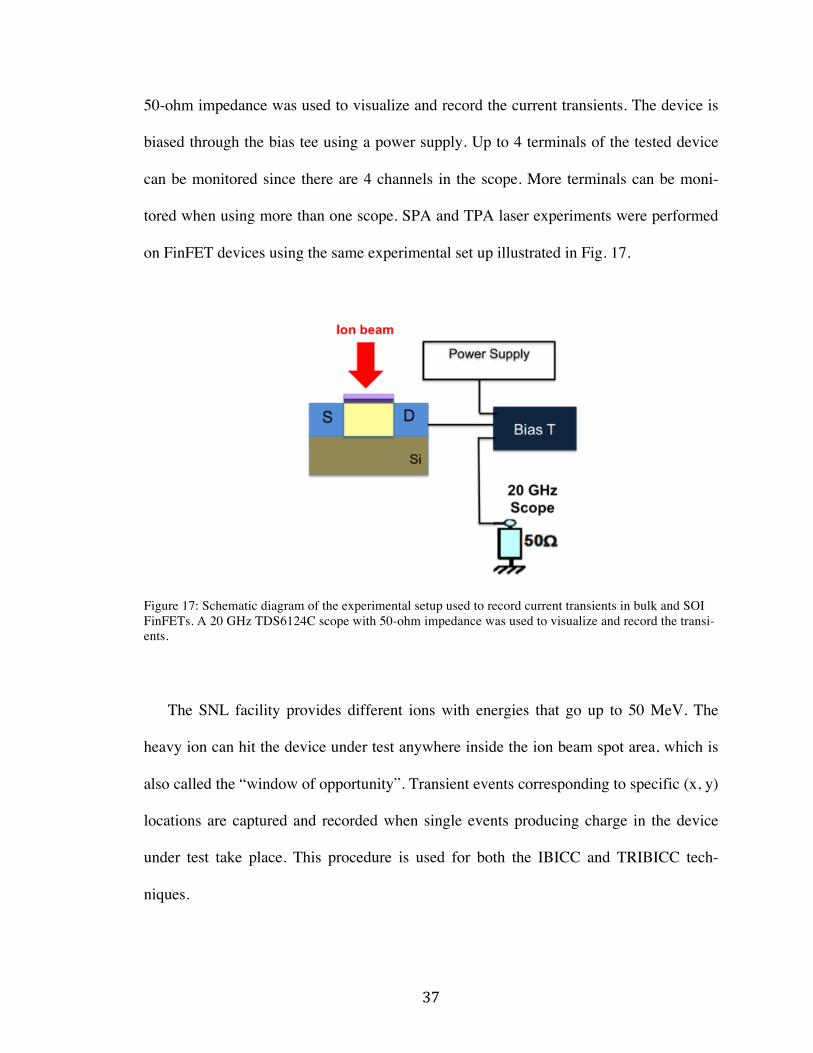
37
50-ohm impedance was used to visualize and record the current transients. The device is
biased through the bias tee using a power supply. Up to 4 terminals of the tested device
can be monitored since there are 4 channels in the scope. More terminals can be moni-
tored when using more than one scope. SPA and TPA laser experiments were performed
on FinFET devices using the same experimental set up illustrated in Fig. 17.
Figure 17: Schematic diagram of the experimental setup used to record current transients in bulk and SOI FinFETs. A 20 GHz TDS6124C scope with 50-ohm impedance was used to visualize and record the transi-ents.
The SNL facility provides different ions with energies that go up to 50 MeV. The
heavy ion can hit the device under test anywhere inside the ion beam spot area, which is
also called the “window of opportunity”. Transient events corresponding to specific (x, y)
locations are captured and recorded when single events producing charge in the device
under test take place. This procedure is used for both the IBICC and TRIBICC tech-
niques.
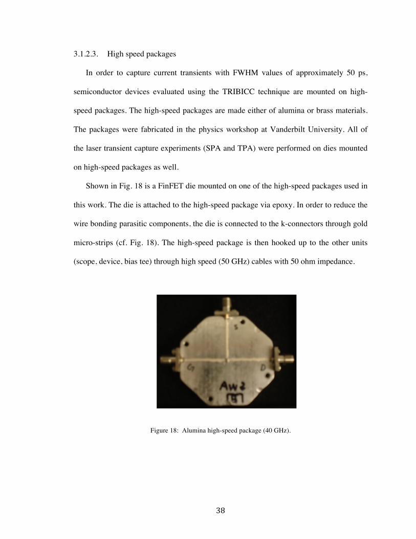
38
3.1.2.3. High speed packages
In order to capture current transients with FWHM values of approximately 50 ps,
semiconductor devices evaluated using the TRIBICC technique are mounted on high-
speed packages. The high-speed packages are made either of alumina or brass materials.
The packages were fabricated in the physics workshop at Vanderbilt University. All of
the laser transient capture experiments (SPA and TPA) were performed on dies mounted
on high-speed packages as well.
Shown in Fig. 18 is a FinFET die mounted on one of the high-speed packages used in
this work. The die is attached to the high-speed package via epoxy. In order to reduce the
wire bonding parasitic components, the die is connected to the k-connectors through gold
micro-strips (cf. Fig. 18). The high-speed package is then hooked up to the other units
(scope, device, bias tee) through high speed (50 GHz) cables with 50 ohm impedance.
Figure 18: Alumina high-speed package (40 GHz).

39
3.2. Devices
In this work, I use FinFETs from two different manufacturers, imec and Texas In-
struments (TI). The p-channel TI FinFETs are test structures with large dimensions (fwidth
= 150 nm, LG = 125 nm) that are built on SOI substrates. These devices were tested with
the objective of comparing them to p-channel bulk FinFETs obtained from imec (two dif-
ferent generations). The first generation contained p-channel bulk FinFETs with large
dimensions (fwidth = 160 nm, LG = 130 nm). The TI and imec p-channel SOI and bulk Fin-
FETs were evaluated using topside and backside laser testing. The second generation of
imec FinFETs comprises sub-70 nm bulk and SOI FinFETs with fin widths as small as 5
nm and gate lengths as short as 20 nm. These FinFETs were evaluated using heavy ion
testing for devices with different drain region architecture for both bulk and SOI. imec
bulk FinFETs with dumbbell and saddle contacts were investigated. The dumbbell layout
is identical to that of a planar MOSFET contact. The saddle contact, however, touches the
top surface as well as the sidewall surfaces of the fin. A schematic diagram along with
additional details of dumbbell and saddle contacts are presented in the last chapter. Table.
1 summarizes the different FinFETs that have been tested in this work:

40
Table 1: Details of the tested FinFETs in this work. FF is FinFET, 1st refers to the first generation, 2nd refers to the second generation, LG is the gate length and FW is the fin width. Technology Polarity LG (nm) FW (nm) Measurement
technique
TI FF SOI p-channel 125 150 SPA
imec FF (1st ) Bulk p-channel 130 160 SPA and
TPA
imec FF (2nd )
Dumbbell contact
Bulk n-channel 70 5-20 IBICC and
TRIBICC
imec FF (2nd)
Saddle contact
Bulk and SOI n-channel 20-60 10-20 IBICC and
TRIBICC
41
CHAPTER IV
LASER INDUCED CURRENT TRANSIENTS IN SUB-130 nm BULK AND SOI FINFETS
Through-wafer two-photon absorption laser experiments are performed on bulk Fin-
FETs. The current transients show distinct signatures for charge collection from drift and
diffusion, demonstrating the contribution of charge generated in the substrate to the
charge collection process. The drain region dominates the charge collection process in
these structures, with maximum collected charge obtained underneath the drain region.
Topside single photon absorption experiments were performed on bulk and SOI Fin-
FETs with the lowest amount of charge collected obtained in SOI FinFETs.
4.1. Bulk FinFETs
4.1.1. Device and experimental details
P-channel bulk FinFETs, manufactured at imec (Leuven, Belgium) were investigated
by means of through-wafer two photon absorption (TPA) technique. These samples have
130 nm gate lengths, 65 nm fin electrical height (i.e., the part of the fin wrapped around
by the gate), 200 nm fin spacing, 160 nm fin width, and there are 10 fins in parallel. The
gate oxide consists of a 2.5 nm HfSiON layer on top of a 1 nm SiO2 interfacial layer. A
100-nm polysilicon layer forms the gate electrode. The source/drain access region is
formed by Ni silicidation.

42
Figure 19: SEM picture of a 10-fins bulk FinFET. The figure shows the fin width (FW) and the gate length (Lg) parameters. The inset shows the cross section of the bulk FinFET corresponding to one fin [12].
Fig. 19 illustrates an SEM picture of a 10-fin bulk FinFET structure including the
drain, source and gate pads. The figure shows the fin width (FW) and the gate length (Lg)
parameters. The inset in Fig. 19 shows the cross section of the bulk FinFET correspond-
ing to one fin.
In contrast to Single-Photon Absorption (SPA) or topside laser testing, which gener-
ates charge in a well-defined (x, y) location [64], TPA or backside laser irradiation, al-
lows controlling the location of the generated charge in the z-direction as well. This ena-
bles the generated carrier dynamics to be investigated in regions topped with metal lay-
ers, where topside laser testing is not possible since the metal layers block the laser light.
The laser beam is focused using a (×100) microscope objective to a spot diameter of 1.6
µm. Laser pulses with wavelength of 1.26 µm and pulse width of 120 fs were used [59].
The transient events were measured using the experimental setup shown in Fig. 17 (chap.
43
4 sec. 3.1.2.2). The samples were mounted in high-speed (50 GHz) packages (i.e., Fig.
18, chap. 4, sec. 3.1.2.3), which were fixed on a stage with 0.1 µm resolution. A 12 GHz
TDS6124C oscilloscope with 50 impedance was used to visualize and record the transi-
ents. The single shot oscilloscope was externally triggered by the laser source.
The p-channel bulk FinFETs were biased through a 50 GHz bias tee in the off-state
configuration with a drain bias of -0.6 V, and with the source, gate and substrate ground-
ed. There is no external well contact for these devices.
4.1.2. Current transients in the drain region
Illustrated in Fig. 20 is Physical structure of the FinFET showing the location of the laser
spot in the fin and up to 30 µm away from the fin. The inset in Fig. 20 shows the SEM
picture of the whole bulk FinFET structure including the gate drain and source terminals.
Figures are not to scale. Fig. 21 shows representative current transients recorded in the
fins (x = 0 µm), and up to 30 µm away from the fins underneath the drain of the p-
channel FinFETs (cf., Fig. 21). The position x = 0 µm is defined when the laser is fo-
cused in the fins (above the gate). Transients in the drain region up to 30 µm from the
fins were recorded and analyzed. 9.3-nJ/pulse irradiation was used for these measure-
ments. Fig. 21 illustrates the evolution of the transient’s shape as the laser moves from
the fins toward the drain region. Transients with smaller amplitudes and longer tails are
captured in the drain region. Transients in Fig. 21 exhibit tails extending up to 40 ns in
the fins. This value increases to 70 ns for transients captured in the drain region. These
tails contain up to 70% of the total charge collected, and are indicative of diffusive charge
collection from the substrate in addition to the drift collection of charge generated in the

44
fins. The diffusion component of the current transients increases as the laser moves fur-
ther from the fins until it completely dominates the transient response as illustrated in
Fig. 20.
Figure 20: Physical structure of the FinFET showing the location of the laser spot in the fin and up to 30 µm away from the fin. Inset: SEM picture of the whole bulk FinFET structure including the gate drain and source terminals. Figures are not to scale [12].
Figure 21: Representative semi log current transients recorded in the fins (x = 0-µm) and up to 30-µm un-derneath the drain away from the fins [12].
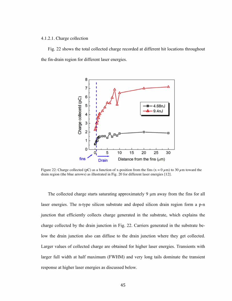
45
4.1.2.1. Charge collection
Fig. 22 shows the total collected charge recorded at different hit locations throughout
the fin-drain region for different laser energies.
Figure 22: Charge collected (pC) as a function of x-position from the fins (x = 0 µm) to 30 µm toward the drain region (the blue arrows) as illustrated in Fig. 20 for different laser energies [12].
The collected charge starts saturating approximately 9 µm away from the fins for all
laser energies. The n-type silicon substrate and doped silicon drain region form a p-n
junction that efficiently collects charge generated in the substrate, which explains the
charge collected by the drain junction in Fig. 22. Carriers generated in the substrate be-
low the drain junction also can diffuse to the drain junction where they get collected.
Larger values of collected charge are obtained for higher laser energies. Transients with
larger full width at half maximum (FWHM) and very long tails dominate the transient
response at higher laser energies as discussed below.

46
4.1.2.2. Charge collection mechanisms
Fig. 23 shows the FWHM values as a function of distance for two laser energies, 4.68
nJ and 9.4 nJ.
Figure 23: Full width at half maximum (FWHM) (ns) as a function of the distance x (µm) for two laser energies: 4.68 nJ and 9.4 nJ. At x = 0 µm, the laser is focused in the fins [12].
Current transients with 100 ps FWHM were obtained when the laser was focused in
the fins. This value increases approximately linearly up to 2 ns at the distance 5 µm. As
the laser spot moves away from the fins toward the drain, the junction drain-substrate (cf.
Fig. 19) dominates the charge collection process, which explains the larger FWHM val-
ues. For distances larger than 5 µm, the FWHM tends to saturate at around 2 ns. At x = 5
µm, the laser spot is entirely contained in the drain region, where the collection volume is
similar throughout the drain substrate junction, hence the saturation of the FWHM curve.
The same trend is obtained for higher laser energies (9.4 nJ) with higher FWHM values.

47
The laser beam has a Gaussian spatial profile. At higher laser energies, the intensity of
the laser in the wings of the Gaussian beam is sufficiently high to produce significant
charge collection [65]. Carriers from deeper in the substrate diffuse to the drain-substrate
junction where they get collected, increasing both the FWHM values and the transients’
tails at higher laser energies.
4.1.3. Current transients in the fins region
Fig. 24(a) illustrates the charge collected as a function of the laser position for 3 dif-
ferent laser energies, 0.98 nJ, 4.68 nJ and 8.2 nJ. Fig. 24(b) shows the SEM picture of the
fin region, illustrating the distance (from 0 µm to 7 µm) traversed by the laser during the
scan. Fig. 24(b) also shows the laser spot at the center of the FinFET structure, at a dis-
tance of ~ 3 µm where the collected charge curves peak (cf. Fig. 24(a)). The width of the
collected charge curves in Fig. 24(a) covers the length of the gate (~ 3.6 µm), considering
a fin-to-fin spacing of 200 nm and a fin width of 160 nm. The collected charge curves
peak at 200 fC at a distance of 3 µm, which corresponds approximately to the center of
the device (cf. Fig. 24(b)). For distances less than 1 µm or greater than 5 µm, the laser
covers fewer fins than it does when positioned near the center of the fin region. Less
charge is collected when fewer fins contribute to charge collection, as shown in Fig.
24(a).
Fig. 25 shows current transients recorded at distances of 3 µm and 5 µm (cf. Fig.
24(b)). At 3 µm, the laser spot (diameter = 1.6 µm) is entirely contained inside the Fin-
FET structure, as illustrated in Fig. 24(b). The laser light covers the maximum number of
fins. However, at 5 µm, the laser light is not completely contained within the gate region
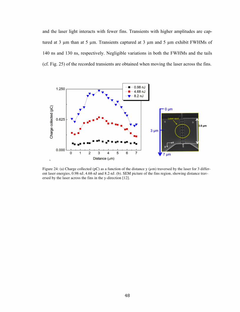
48
and the laser light interacts with fewer fins. Transients with higher amplitudes are cap-
tured at 3 µm than at 5 µm. Transients captured at 3 µm and 5 µm exhibit FWHMs of
140 ns and 130 ns, respectively. Negligible variations in both the FWHMs and the tails
(cf. Fig. 25) of the recorded transients are obtained when moving the laser across the fins.
Figure 24: (a) Charge collected (pC) as a function of the distance y (µm) traversed by the laser for 3 differ-ent laser energies, 0.98-nJ, 4.68-nJ and 8.2-nJ. (b). SEM picture of the fins region, showing distance trav-ersed by the laser across the fins in the y-direction [12].

49
Figure 25: Current transients captured in the fins at distances: 3 µm and 5 µm (cf. Fig. 22(b)) for laser en-ergy of 0.89 nJ [12].
However, significant modulation of the transient’s amplitude is observed, suggesting a
strong contribution of the fins to charge collection in the structure. Fast transients with
large amplitudes are produced in the fins due to the high electric field. Transients cap-
tured at the same locations at higher laser energy are plotted in Fig. 26.

50
Figure 26: Current transients captured in the fins at distances: 3 µm and 5 µm (cf. Fig. 6(b)) for a laser en-ergy of 4.68 nJ [12].
Transients with larger FWHMs and longer tails are recorded at higher laser energy
(4.68 nJ). However, no significant variation in either parameter when moving the laser
across the fins is observed. These results clearly illustrate the fins’ contribution to charge
collection. This result can affect the switching behavior of high-performance FinFET
based circuits, where fast transients with large amplitudes are more likely to produce up-
sets than transients with smaller amplitudes but higher total charge.
4.2. Bulk vs. SOI FinFETs
4.2.1. Device and experimental details
Similar PMOS bulk FinFETs to those evaluated with TPA techniques in the previous
section of this chapter were tested using SPA technique. The obtained results of bulk
FinFETs are then compared to SPA results obtained in SOI FinFETs with similar dimen-
sions.
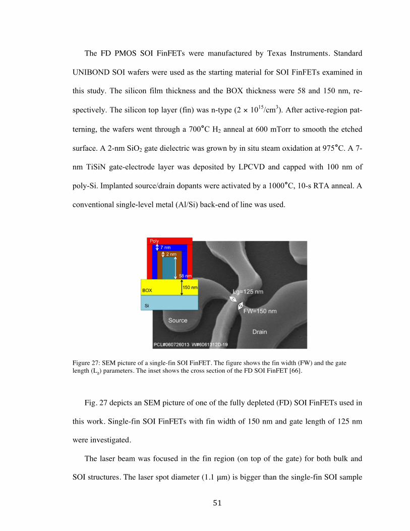
51
The FD PMOS SOI FinFETs were manufactured by Texas Instruments. Standard
UNIBOND SOI wafers were used as the starting material for SOI FinFETs examined in
this study. The silicon film thickness and the BOX thickness were 58 and 150 nm, re-
spectively. The silicon top layer (fin) was n-type (2 × 10¹⁵/cm3). After active-region pat-
terning, the wafers went through a 700°C H2 anneal at 600 mTorr to smooth the etched
surface. A 2-nm SiO2 gate dielectric was grown by in situ steam oxidation at 975°C. A 7-
nm TiSiN gate-electrode layer was deposited by LPCVD and capped with 100 nm of
poly-Si. Implanted source/drain dopants were activated by a 1000°C, 10-s RTA anneal. A
conventional single-level metal (Al/Si) back-end of line was used.
Figure 27: SEM picture of a single-fin SOI FinFET. The figure shows the fin width (FW) and the gate length (Lg) parameters. The inset shows the cross section of the FD SOI FinFET [66].
Fig. 27 depicts an SEM picture of one of the fully depleted (FD) SOI FinFETs used in
this work. Single-fin SOI FinFETs with fin width of 150 nm and gate length of 125 nm
were investigated.
The laser beam was focused in the fin region (on top of the gate) for both bulk and
SOI structures. The laser spot diameter (1.1 μm) is bigger than the single-fin SOI sample
52
dimensions (W/L = 150/125), as illustrated in Fig. 27. Thus, charge is generated in the
entire active region of the SOI sample (i.e., fin). However, the bulk FinFET has ten fins,
as shown in Fig. 19. The laser spot covers approximately four fins of the bulk device. A
similar set up to that used for TPA measurement was utilized for the SPA experiment (cf.
sec. 4.1.1). Devices were irradiated in the off state configuration with a drain bias of -0.6
V, and the source, drain and substrate grounded. The body in the SOI FinFETs was left
floating.
4.2.2. Laser induced current transients in bulk and SOI FinFETs
Fig. 28 illustrates the recorded current transients at the drain terminals for both bulk
and SOI FinFETs for a laser energy of 22.4 pJ. Larger and longer transients are exhibited
by the bulk FinFETs. A full width at half maximum (FWHM) of 80 ps was obtained for
the SOI samples. Larger and faster current transients (67 ps) were recorded for gamma-
shaped SOI n-channel FinFETs with thinner fins (25 nm) [55] than those used in this
work (58 nm). The higher amplitude current transient for the bulk FinFET is partially due
to the additional three fins contributing to charge collection in bulk samples. A FWHM
value of 310 ps was recorded for the bulk FinFETs, which is three times larger than the
value obtained for the SOI FinFETs.

53
Figure 28: Semi log drain current transients generated by the pulsed laser in both SOI and bulk FinFETs. The laser energy is 22.4 pJ. A voltage of -0.6 V was applied to both samples during irradiation. The full width at half maximum (FWHM) is illustrated for both devices on the figure [66].
Fig. 28 also shows a tail extending over more than 4 ns. This is caused by carrier dif-
fusion from the substrate to the fins where they are collected. This carrier diffusion is
eliminated in the case of SOI FinFETs where the active region (fins) is isolated from the
substrate. Similar SPA experiments performed on 0.25 µm bulk planar MOSFETs exhib-
ited current transients with smaller FWHM values and reduced tails [50] than those ob-
served in Fig. 28. The FinFETs used in this section are development devices. The large
drain regions (180 µm x 180 µm) in the tested bulk FinFETs may produce the observed
large FWHM values and long tails in the current transients.
4.2.3. Laser energy dependence of the charge collection
Fig. 29 illustrates the charge collected for both FinFET technologies as a function of
the laser energy.
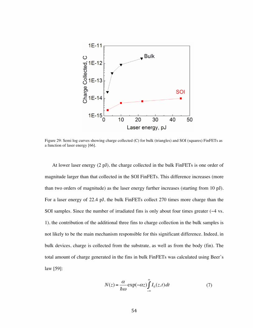
54
Figure 29: Semi log curves showing charge collected (C) for bulk (triangles) and SOI (squares) FinFETs as a function of laser energy [66].
At lower laser energy (2 pJ), the charge collected in the bulk FinFETs is one order of
magnitude larger than that collected in the SOI FinFETs. This difference increases (more
than two orders of magnitude) as the laser energy further increases (starting from 10 pJ).
For a laser energy of 22.4 pJ, the bulk FinFETs collect 270 times more charge than the
SOI samples. Since the number of irradiated fins is only about four times greater (~4 vs.
1), the contribution of the additional three fins to charge collection in the bulk samples is
not likely to be the main mechanism responsible for this significant difference. Indeed, in
bulk devices, charge is collected from the substrate, as well as from the body (fin). The
total amount of charge generated in the fins in bulk FinFETs was calculated using Beer’s
law [59]:
(7) N(z) = !!!exp(!"z) I0 (z, t)dt
!"
"
#
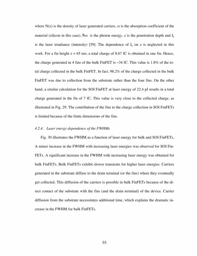
55
where N(z) is the density of laser generated carriers, α is the absorption coefficient of the
material (silicon in this case), ħω is the photon energy, z is the penetration depth and I0
is the laser irradiance (intensity) [59]. The dependence of I0 on z is neglected in this
work. For a fin height z = 65 nm, a total charge of 8.67 fC is obtained in one fin. Hence,
the charge generated in 4 fins of the bulk FinFET is ~34 fC. This value is 1.8% of the to-
tal charge collected in the bulk FinFET. In fact, 98.2% of the charge collected in the bulk
FinFET was due to collection from the substrate rather than the four fins. On the other
hand, a similar calculation for the SOI FinFET at laser energy of 22.4 pJ results in a total
charge generated in the fin of 7 fC. This value is very close to the collected charge, as
illustrated in Fig. 29. The contribution of the fins to the charge collection in SOI FinFETs
is limited because of the finite dimensions of the fins.
4.2.4. Laser energy dependence of the FWHMs
Fig. 30 illustrates the FWHM as a function of laser energy for bulk and SOI FinFETs.
A minor increase in the FWHM with increasing laser energies was observed for SOI Fin-
FETs. A significant increase in the FWHM with increasing laser energy was obtained for
bulk FinFETs. Bulk FinFETs exhibit slower transients for higher laser energies. Carriers
generated in the substrate diffuse to the drain terminal (or the fins) where they eventually
get collected. This diffusion of the carriers is possible in bulk FinFETs because of the di-
rect contact of the substrate with the fins (and the drain terminal) of the device. Carrier
diffusion from the substrate necessitates additional time, which explains the dramatic in-
crease in the FWHM for bulk FinFETs.

56
Figure 30: Semi log plot showing FWHM as a function of laser energy for bulk (empty squares) and SOI FinFETs (empty triangles) [66].
In SOI FinFETs, charge gets collected only from the fins since the buried oxide iso-
lates the active region from the substrate. Additional amplification effects are likely to
contribute to the observed charge enhancement in bulk FinFETs. It has been reported, as
explained in chapter III, that bulk devices can be vulnerable to bipolar effects. It is possi-
ble that bipolar amplification could contribute to the charge collection in the bulk Fin-
FETs investigated in this section, since obvious drain bias dependence of the charge col-
lection was observed in these FinFETs, as shown in the next paragraph.
4.2.5. Drain bias dependence of the charge collection
Transients were captured for different drain biases while irradiating the FinFETs.
Transients with larger amplitudes were obtained with increasing drain bias for both bulk
and SOI FinFETs. Higher drain biases produce higher electric fields in the fins, which
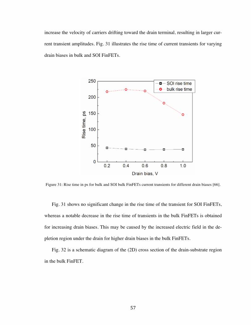
57
increase the velocity of carriers drifting toward the drain terminal, resulting in larger cur-
rent transient amplitudes. Fig. 31 illustrates the rise time of current transients for varying
drain biases in bulk and SOI FinFETs.
Figure 31: Rise time in ps for bulk and SOI bulk FinFETs current transients for different drain biases [66].
Fig. 31 shows no significant change in the rise time of the transient for SOI FinFETs,
whereas a notable decrease in the rise time of transients in the bulk FinFETs is obtained
for increasing drain biases. This may be caused by the increased electric field in the de-
pletion region under the drain for higher drain biases in the bulk FinFETs.
Fig. 32 is a schematic diagram of the (2D) cross section of the drain-substrate region
in the bulk FinFET.
58
Figure 32: Schematic diagram of the (2D) cross section of the drain-substrate region in the bulk FinFET [66].
When increasing the drain bias, the depletion region expands more into the substrate.
This results in a higher peak electric field in the depletion region. This increase in the
electric field accelerates the collection of carriers, which decreases the rise time in bulk
FinFETs for increasing drain bias. This result can be a signature of the substrate effects in
charge collection of bulk FinFETs.
The results of these laser experiments are useful to determine the sensitive volumes of
the bulk FinFETs, and to explore the charge collection mechanisms in these structures.
However, the large laser spot size (1.6 µm for TPA and 1.1 µm for SPA) covers parts of
the drain and source regions in addition to the fins, as shown in the inset of Fig. 19. This
enhances the substrate contribution to the collected charge, masking the intrinsic transient
response of the FinFET structure. In order to gain additional insight into the charge col-
lection mechanisms, in particular as they are manifested in highly scaled bulk FinFETs,
the IBICC and TRIBICC methods were used on state of the art bulk FinFETs. The devic-
es used for the IBICC and TRIBICC experiments were NMOSFETs, unlike the
59
PMOSFETs used for the SPA and TPA experiments. The difference in polarity does not
affect the qualitative nature of the results reported here, in particular, the effects of strike
location on charge collection. The collected charge measured using the IBICC and
TRIBICC experiments results from the passage of a single ion at a time through the Fin-
FET. The collected charge measured using the laser (SPA and/or TPA) experiments,
however, is more challenging to interpret when testing highly scaled FinFETs since the
laser spot size is comparable (or greater) to the whole FinFET structure.
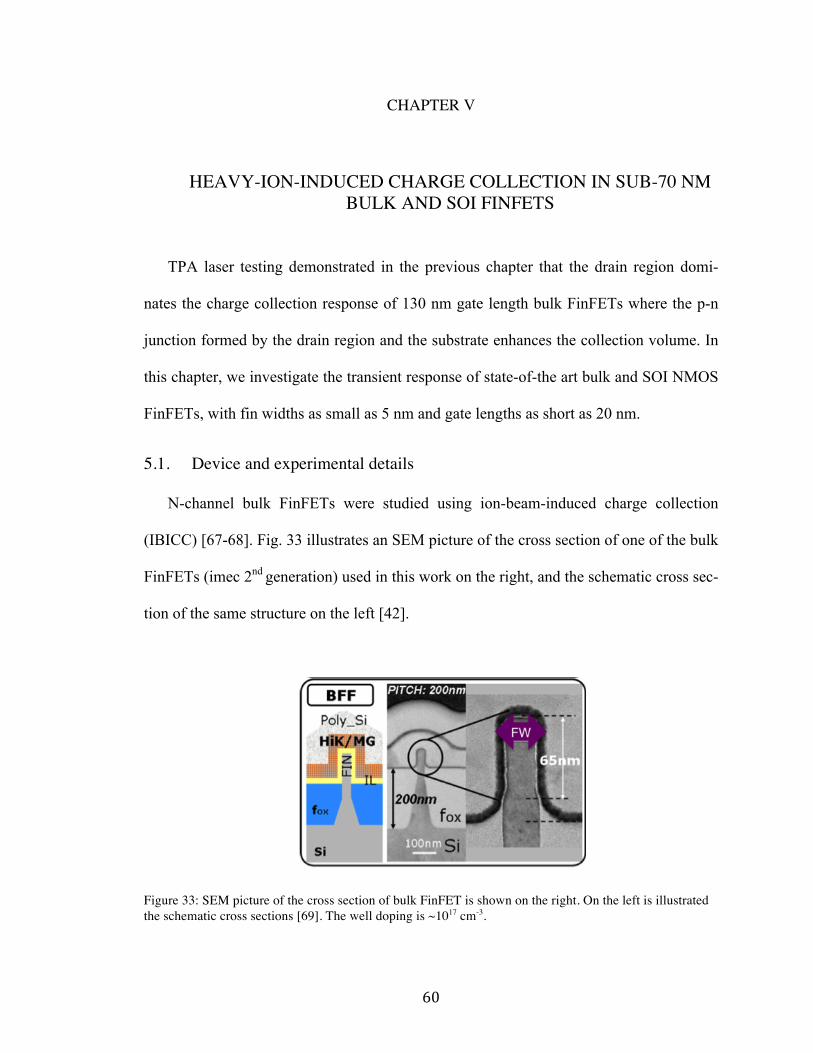
60
CHAPTER V
HEAVY-ION-INDUCED CHARGE COLLECTION IN SUB-70 NM BULK AND SOI FINFETS
TPA laser testing demonstrated in the previous chapter that the drain region domi-
nates the charge collection response of 130 nm gate length bulk FinFETs where the p-n
junction formed by the drain region and the substrate enhances the collection volume. In
this chapter, we investigate the transient response of state-of-the art bulk and SOI NMOS
FinFETs, with fin widths as small as 5 nm and gate lengths as short as 20 nm.
5.1. Device and experimental details
N-channel bulk FinFETs were studied using ion-beam-induced charge collection
(IBICC) [67-68]. Fig. 33 illustrates an SEM picture of the cross section of one of the bulk
FinFETs (imec 2nd generation) used in this work on the right, and the schematic cross sec-
tion of the same structure on the left [42].
Figure 33: SEM picture of the cross section of bulk FinFET is shown on the right. On the left is illustrated the schematic cross sections [69]. The well doping is ~1017 cm-3.

61
The devices have 50 nm electrical fin height, 200 nm fin pitch, and 5 to 10 fins in
parallel. The gate length ranges from 20 nm to 70 nm. FinFETs with fin widths from 20
nm down to 5 nm were examined. The devices feature a high-k gate dielectric (2.3 nm
HfSiO2 on 1 nm interfacial oxide) and 100 nm of polysilicon on top of a 5 nm TiN metal
gate. The source/drain access region is formed by Selective Epitaxial Growth (SEG) of Si
on the source and drain areas, followed by NiPt silicidation.
The ion beam was focused to 1.5 µm × 0.7 µm and scanned over a 20 µm ×20 µm
area with a step size of 100 nm. Values of the charge collected were obtained for every
location of the scanned area. 42 MeV copper ions with a linear energy transfer (LET) at
the surface of 27.5 MeV-cm2/mg and a range in silicon of 10 µm were used. This ensures
the passage of the ion through the active layers of the FinFET structure. The total charge
collected at the drain terminal was measured with a preamplifier that integrates transient
signals at the monitored terminal. An identical copper ion beam was used for SOI Fin-
FET IBICC measurements in the following section.
A drain bias of 0.6 V (unless otherwise mentioned) was applied for these n-channel
FinFETs during irradiation. The gate, source, well and substrate were grounded.
5.2. Charge collection in bulk FinFETs
Fig. 34(a) illustrates 20 µm × 20 µm scan results of the charge collected at the drain
terminal as a function of the ion strike location for an NMOS bulk FinFET. Fig. 34(b)
shows the projection of the charge collection on the (x, y) plane. Fig. 34(b) defines the
sensitive area, with the maximum charge collection occurring in the drain region of the
FinFET structure. A sensitive area of 4 µm × 2 µm can be measured according to Fig.
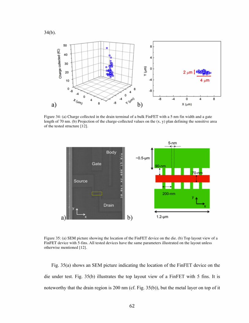
62
34(b).
Figure 34: (a) Charge collected in the drain terminal of a bulk FinFET with a 5 nm fin width and a gate length of 70 nm. (b) Projection of the charge-collected values on the (x, y) plan defining the sensitive area of the tested structure [12].
Figure 35: (a) SEM picture showing the location of the FinFET device on the die. (b) Top layout view of a FinFET device with 5-fins. All tested devices have the same parameters illustrated on the layout unless otherwise mentioned [12].
Fig. 35(a) shows an SEM picture indicating the location of the FinFET device on the
die under test. Fig. 35(b) illustrates the top layout view of a FinFET with 5 fins. It is
noteworthy that the drain region is 200 nm (cf. Fig. 35(b)), but the metal layer on top of it

63
is 400 nm wide. Hence, the actual dimensions of the drain region are 1.2 µm x 0.5 µm.
The correspondence between the region of maximum charge collection and the drain is
not exact because of the asymmetric ion beam spot size (1.5 µm x 0.7 µm). The ion can
hit the device in any location inside this window (i.e., the window of opportunity). The
measured sensitive area in Fig. 34(b) is the result of a convolution of the drain area and
the beam’s window of opportunity.
Figure 36: Projected values of the charge collected (fC) shown in Fig. 2(a) on the x-axis (µm) [12].
Fig. 36 illustrates values of the charge collected at the drain terminal in Fig. 34(a) on
the x-axis. These results suggest that the peak of the collected charge, which is approxi-
mately 45 fC for this particular device, occurs in the drain region. The maximum charge
generated in a single fin after the passage of a copper ion is 14 fC, which is about three
times less than the collected charge. This result confirms the previously obtained laser
data, highlighting the importance of the drain region’s contribution to charge collection in
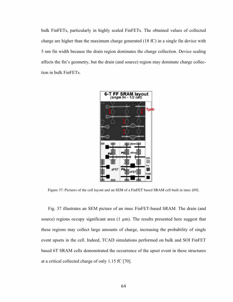
64
bulk FinFETs, particularly in highly scaled FinFETs. The obtained values of collected
charge are higher than the maximum charge generated (18 fC) in a single fin device with
5 nm fin width because the drain region dominates the charge collection. Device scaling
affects the fin’s geometry, but the drain (and source) region may dominate charge collec-
tion in bulk FinFETs.
Figure 37: Pictures of the cell layout and an SEM of a FinFET based SRAM cell built in imec [69].
Fig. 37 illustrates an SEM picture of an imec FinFET-based SRAM. The drain (and
source) regions occupy significant area (1 µm). The results presented here suggest that
these regions may collect large amounts of charge, increasing the probability of single
event upsets in the cell. Indeed, TCAD simulations performed on bulk and SOI FinFET
based 6T SRAM cells demonstrated the occurrence of the upset event in these structures
at a critical collected charge of only 1.15 fC [70].

65
5.2. Charge collected in SOI FinFETs
N-channel SOI FinFETs were evaluated using the IBICC technique. SOI FinFETs
were fabricated using the same mask used for the bulk FinFETs investigated in the previ-
ous paragraph of this chapter. The SOI FinFETs have similar top layout as that of the
bulk FinFETs (cf. Fig. 35) and the same number of fins. A buried oxide layer of 150 nm
was used to isolate the fins from the substrate.
Figure 38: SEM picture of the cross section of SOI FinFET is shown on the right. On the left is illustrated the schematic cross sections [69].
Fig. 38 illustrates SEM pictures and schematic cross sections of one of the SOI Fin-
FET (imec 2nd generation). Both bulk and SOI FinFETs were built on a p-type substrate
with a doping of 4 × 1015 cm-3. A drain bias of 1 V was applied for these n-channel SOI
FinFETs during irradiation. The gate, source, and substrate were grounded. The body was
left floating.
5.2.1. IBICC experimental results
Fig. 34b in the previous section showed that IBICC experiments performed on bulk
66
FinFETs showed that the most sensitive region of these structures maps reasonably well
to the drain region indicating the significant contribution of the drain region in the charge
collection process. The transient response of SOI FinFETs is still not well understood.
However, SOI FinFETs are expected to be more tolerant to SEEs in comparison to their
bulk counterparts thanks to the BOX layer that reduces their collection volume to the
fins. SOI FinFETs with fin width smaller than 20 nm did not exhibit any measurable tran-
sient events in contrast to bulk FinFETs, where events were recorded in devices with fin
widths as narrow as 5 nm (cf. Fig. 34).
Plotted in Fig. 39 is charge collected at the drain (stars), source (triangles) and in the
substrate (circles) terminals of an SOI FinFET with a grounded substrate (0 V). The
amounts of charge collected at the drain are higher than that generated in the fin, which is
about 18 fC. Values of the charge collected in the drain are comparable to those recorded
in the substrate terminal of the irradiated SOI FinFET. These somewhat unexpected re-
sults agree with previous work on planar structures where the substrate effect was
demonstrated to have a notable impact on the charge collection in SOI structures [71-72].
The existence of a depletion region underneath the BOX in SOI devices causes charge
separation in the substrate, which induces charge to be collected in the drain terminal due
to capacitive coupling.

67
Figure 39: Values of charge collected (fC) along the x-axis (along the gate) in the substrate (circles) source (triangles) and drain (stars) terminals. The SOI FinFET was biased in the off state configuration with a grounded substrate [73].
Figure 40: Values of charge collected (fC) along the x-axis (along the gate) in the substrate (circles) source (triangles) and drain (stars) terminals. The SOI FinFET was biased in the off state configuration with a sub-strate bias of -4V [73].
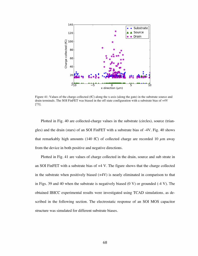
68
Figure 41: Values of the charge collected (fC) along the x-axis (along the gate) in the substrate source and drain terminals. The SOI FinFET was biased in the off state configuration with a substrate bias of +4V [73].
Plotted in Fig. 40 are collected-charge values in the substrate (circles), source (trian-
gles) and the drain (stars) of an SOI FinFET with a substrate bias of -4V. Fig. 40 shows
that remarkably high amounts (140 fC) of collected charge are recorded 10 µm away
from the device in both positive and negative directions.
Plotted in Fig. 41 are values of charge collected in the drain, source and sub strate in
an SOI FinFET with a substrate bias of +4 V. The figure shows that the charge collected
in the substrate when positively biased (+4V) is nearly eliminated in comparison to that
in Figs. 39 and 40 when the substrate is negatively biased (0 V) or grounded (-4 V). The
obtained IBICC experimental results were investigated using TCAD simulations, as de-
scribed in the following section. The electrostatic response of an SOI MOS capacitor
structure was simulated for different substrate biases.

69
5.2.2. TCAD simulation results
Illustrated in Fig. 42 is the schematic cross section of the SOI MOS capacitor used for
TCAD simulations.
Figure 42: Enlarged view of the schematic cross section of the SOI MOS capacitor simulated using TCAD.
The thicknesses of the overlayers shown in Fig. 42 are similar to those of the tested
SOI FinFET. The fin and the substrate are lightly doped (~1015 cm-3) in agreement with
the doping profile of the tested FinFETs. The substrate thickness of the simulated struc-
ture is 10 µm in contrast to the real substrate thickness, which is 700 µm. The obtained
simulation results are independent of the substrate thickness.
Illustrated in Fig. 43 is the schematic cross section of the SOI MOS capacitor with a
grounded substrate. The white line in the substrate of the capacitor is the oxide/substrate
depletion region border. This figure demonstrates the existence of the depletion region
when the substrate is grounded. The poly-fin work-function difference generates an elec-
tric field across the capacitor structure that extends to the substrate, generating the deple-
tion region in Fig. 43. The electric field in the depletion region collects charge after the
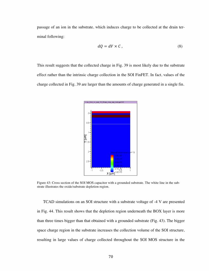
70
passage of an ion in the substrate, which induces charge to be collected at the drain ter-
minal following:
!" = !" × ! , (8)
This result suggests that the collected charge in Fig. 39 is most likely due to the substrate
effect rather than the intrinsic charge collection in the SOI FinFET. In fact, values of the
charge collected in Fig. 39 are larger than the amounts of charge generated in a single fin.
Figure 43: Cross section of the SOI MOS capacitor with a grounded substrate. The white line in the sub-strate illustrates the oxide/substrate depletion region.
TCAD simulations on an SOI structure with a substrate voltage of -4 V are presented
in Fig. 44. This result shows that the depletion region underneath the BOX layer is more
than three times bigger than that obtained with a grounded substrate (Fig. 43). The bigger
space charge region in the substrate increases the collection volume of the SOI structure,
resulting in large values of charge collected throughout the SOI MOS structure in the

71
FinFET device as illustrated in Fig. 40. This effect is considerably mitigated when apply-
ing a positive substrate bias.
Figure 44: Cross section of the SOI MOS capacitor with a substrate voltage of -4 V. The white line in the substrate illustrates the oxide/substrate depletion region.
Figure 45: Cross section of the SOI MOS capacitor with a substrate voltage of +4 V. The absence of the white line in the substrate demonstrates the absence of the depletion region.
72
Fig. 45 shows an SOI MOS structure with a positive substrate bias of 4 V. Fig. 45
demonstrates the absence of the depletion region in the oxide/substrate interface. The
positive substrate bias eliminates the depletion region in the BOX/substrate interface
where an accumulation layer is created instead. This significantly reduces the amount of
charge collected in the substrate, as illustrated in Figs. 40 and 41. Fig. 41 shows, howev-
er, that the drain terminal collects as much as 8 times more charge than that generated in
the fin of the tested FinFET. This suggests the onset of an amplification effect in the test-
ed device. The positive substrate bias (+4 V) may modulate the body potential of the
FinFET device enhancing the parasitic bipolar conduction from the source (emitter) to-
ward the drain (collector). Terminals monitored during IBICC measurements can detect
currents flowing in one direction only. The results illustrated in Fig. 41 were recorded
during IBICC experiment where the polarity of the drain and source terminals was set to
be the same. This explains the absence of charge recorded in the source terminal in Figs.
39 and 41. As a consequence, the observed charge enhancement in Fig. 41 cannot be veri-
fied at this point. In the TRIBICC technique, currents with both polarities can be detected
and measured. The charge amplification effect is investigated in more detail in the next
chapter where bulk and SOI FinFETs with reduced drain areas are evaluated using the
TRIBICC technique.
The obtained heavy-ion data on state-of-the-art bulk FinFETs validated the laser data
presented in the previous chapter. The drain region of advanced bulk FinFETs dominates
the charge collection, with as much as 45 fC of charge collected in the drain region. Ad-
vanced irradiated SOI FinFETs showed to be very vulnerable to the substrate bias. The
IBICC results for the SOI devices show significant substrate effects on the charge collec-

73
tion in SOI FinFETs, which modulates the transient response of these structures.
5.3. Current transients in bulk FinFETs
TRIBICC experiments were performed on bulk FinFETs, identical to the structures il-
lustrated in Fig. 35. The TRIBICC technique is explained in detail in Chapter II.
TRIBICC measurement were performed with a copper ion beam that is similar to the one
used for the IBICC measurements in the previous sections. In this paragraph we explore
the current transients collected at the drain terminal of bulk FinFETs.
Plotted in Fig. 46 is a representative current transient recorded at the drain terminal of
a bulk FinFET biased in the off state with a drain bias of 1 V. The FinFET has 5 fins, as
illustrated in Fig. 35(b); each fin is 20 nm wide and 70 nm long. Similar current wave-
forms to those shown in Fig. 46 were recorded in 5 nm fin width FinFETs. The illustra-
tive current transient in Fig. 46 exhibits the typical drift and diffusion signatures that are
similar to those obtained in gamma shaped SOI FinFET devices [55] with relatively short
tails and small FWHM values. A FWHM of only 75 ps was measured in this bulk Fin-
FET transient thanks to the 20 GHz single shot scope. This value of FWHM is obtained
in the development bulk FinFETs considered here and is expected to change in new gen-
erations of bulk FinFETs. Integration of the current transient illustrated in Fig. 46 results
in a collected charge that is at least 6 times higher that that generated in the fin (20 fC).
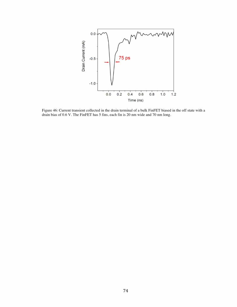
74
Figure 46: Current transient collected in the drain terminal of a bulk FinFET biased in the off state with a drain bias of 0.6 V. The FinFET has 5 fins, each fin is 20 nm wide and 70 nm long.
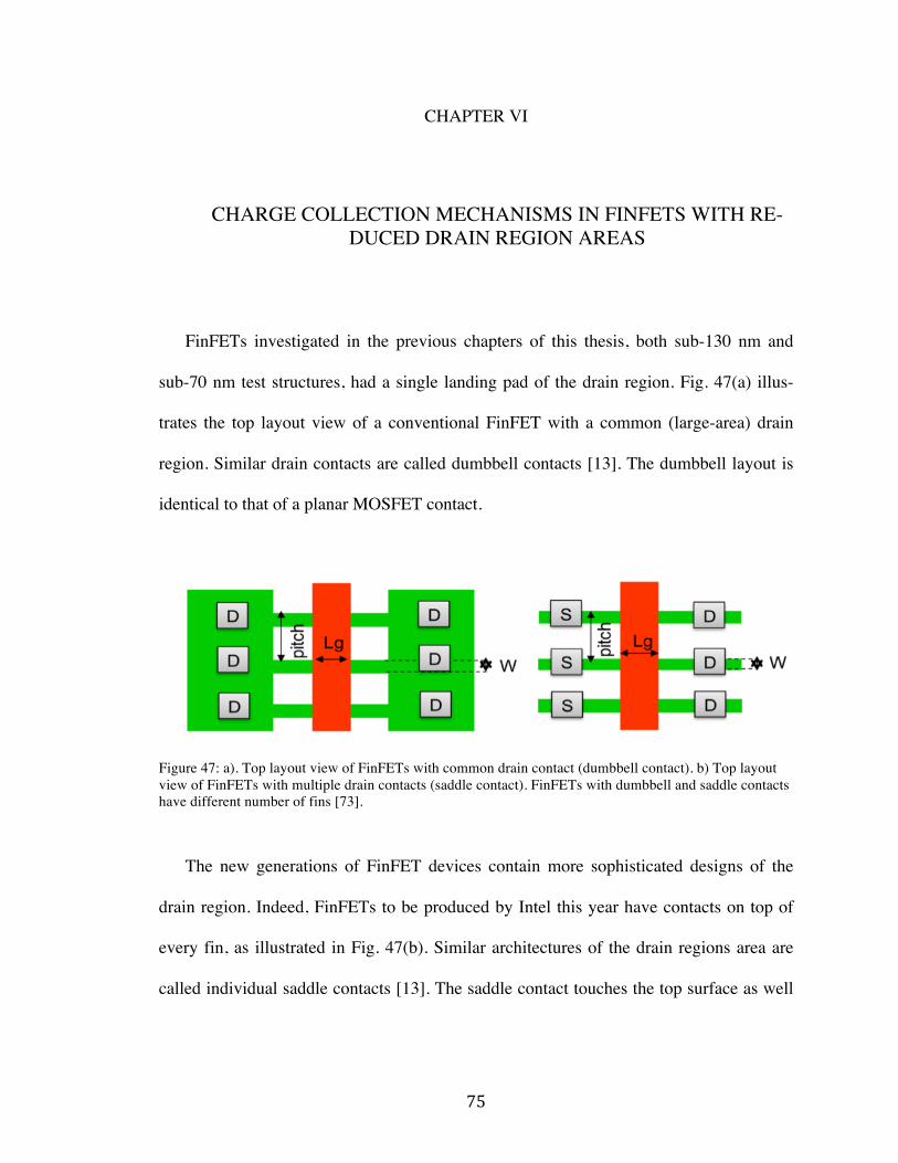
75
CHAPTER VI
CHARGE COLLECTION MECHANISMS IN FINFETS WITH RE-DUCED DRAIN REGION AREAS
FinFETs investigated in the previous chapters of this thesis, both sub-130 nm and
sub-70 nm test structures, had a single landing pad of the drain region. Fig. 47(a) illus-
trates the top layout view of a conventional FinFET with a common (large-area) drain
region. Similar drain contacts are called dumbbell contacts [13]. The dumbbell layout is
identical to that of a planar MOSFET contact.
Figure 47: a). Top layout view of FinFETs with common drain contact (dumbbell contact). b) Top layout view of FinFETs with multiple drain contacts (saddle contact). FinFETs with dumbbell and saddle contacts have different number of fins [73].
The new generations of FinFET devices contain more sophisticated designs of the
drain region. Indeed, FinFETs to be produced by Intel this year have contacts on top of
every fin, as illustrated in Fig. 47(b). Similar architectures of the drain regions area are
called individual saddle contacts [13]. The saddle contact touches the top surface as well

76
as the sidewalls surfaces of the fin. This increases the contact area, which reduces the
contact resistance.
The laser and heavy ion results in the previous chapters demonstrated that the drain
region dominates the transient response of FinFET devices with dumbbell contacts. In
this chapter, we investigate single-event effects in bulk and SOI FinFETs with saddle
contacts using the IBICC and TRIBICC techniques. Heavy-ion data obtained from Fin-
FETs with saddle contacts are compared to that obtained from FinFETs with convention-
al designs (dumbbell) of the drain region. Bulk and SOI FinFETs with saddle contacts are
vulnerable to the charge enhancement effects similar to their counterparts with dumbbell
contacts. This amplification effect is explained in detail through TRIBICC experimental
results.
6.1. Charge collection in FinFETs with saddle contacts
FinFETs with dumbbell and saddle were laid out on the same wafer. Fabrication de-
tails and doping profiles of the FinFETs with saddle contacts are similar to those of the
FinFETs with dumbbell contacts (i.e., chap. V sec. 5.1). In this section we investigate the
IBICC and TRIBICC results of bulk and SOI FinFETs with saddle contacts. Devices with
gate lengths ranging from 20 nm to 60 nm and fin widths ranging from 5 nm to 20 nm
were tested (cf. table 1). The FinFETs with dumbbell contacts have 5 fins in parallel and
the FinFETs with saddle contacts have 10 fins in parallel. The ion beam was scanned
over a 20 µm × 20 µm area with a step size of 100 nm. A copper ion beam with energy of
46 MeV and a spot size of 2.2 µm x 0.9 µm was used. The devices were biased in the off-
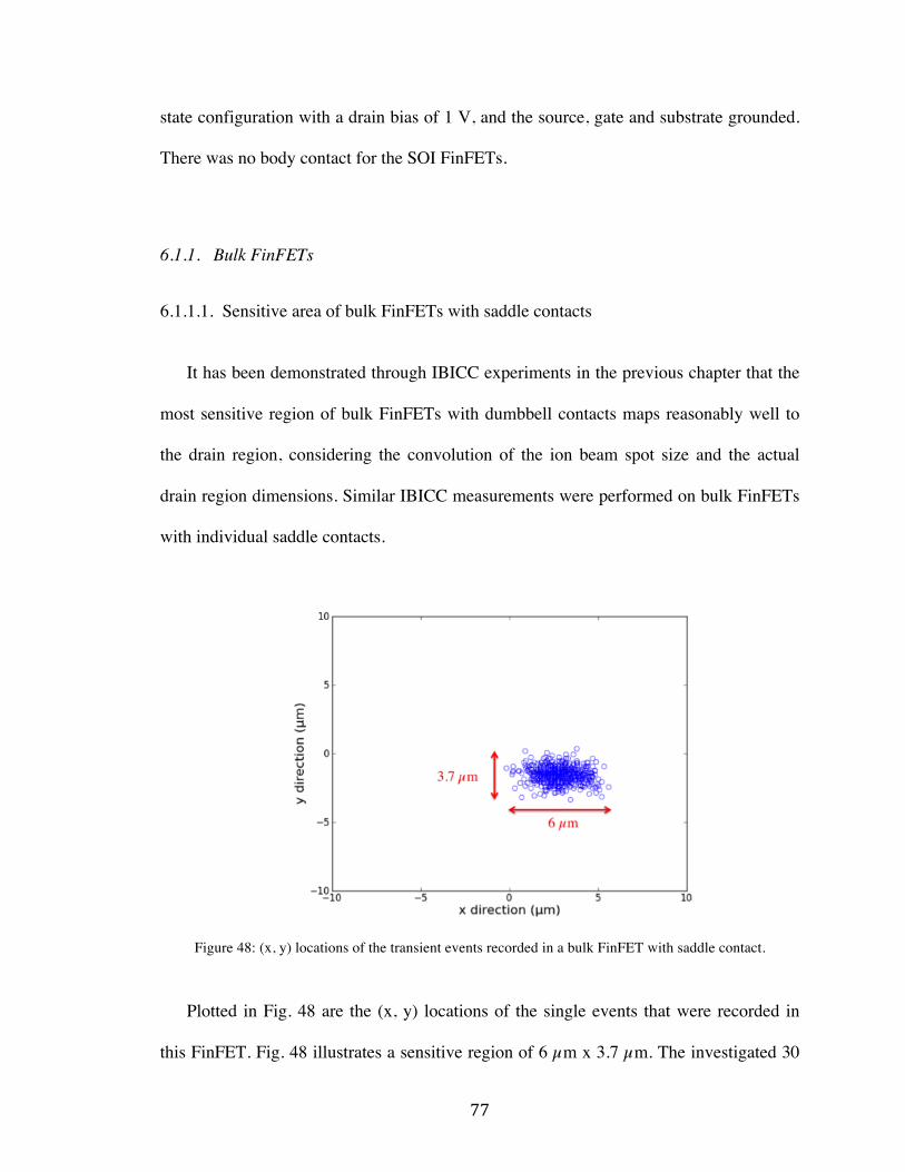
77
state configuration with a drain bias of 1 V, and the source, gate and substrate grounded.
There was no body contact for the SOI FinFETs.
6.1.1. Bulk FinFETs
6.1.1.1. Sensitive area of bulk FinFETs with saddle contacts
It has been demonstrated through IBICC experiments in the previous chapter that the
most sensitive region of bulk FinFETs with dumbbell contacts maps reasonably well to
the drain region, considering the convolution of the ion beam spot size and the actual
drain region dimensions. Similar IBICC measurements were performed on bulk FinFETs
with individual saddle contacts.
Figure 48: (x, y) locations of the transient events recorded in a bulk FinFET with saddle contact.
Plotted in Fig. 48 are the (x, y) locations of the single events that were recorded in
this FinFET. Fig. 48 illustrates a sensitive region of 6 µm x 3.7 µm. The investigated 30
78
nm gate length FinFET has 10 fins, each fin is 15 nm wide with a 200 nm pitch. The
combination of the (10) individual saddle contacts and the oxide (separating the fins) in
the drain region cover a distance of ~1.8 µm in the x direction. The convolution of the
actual drain contact area with the ion beam spot size yields the results in Fig. 48. This
suggests that, similarly to FinFETs with dumbbell contacts, the sensitive region of Fin-
FETs with individual saddle contact maps reasonably well to the drain region. In order to
gain more insights into the transient response of FinFETs with saddle contacts, TRIBICC
measurements were performed on these devices and current transients were recorded.
6.1.1.2. Current transients in bulk FinFETs with saddle contacts
Illustrated in Fig. 49 is a heavy ion-induced maximum current transient obtained from
a bulk FinFET (W/L = 20/70) with dumbbell contacts (solid curve), and one of the largest
current transients recorded in a bulk FinFET (Wf/L=20/60) with saddle contacts (dashed
curve).
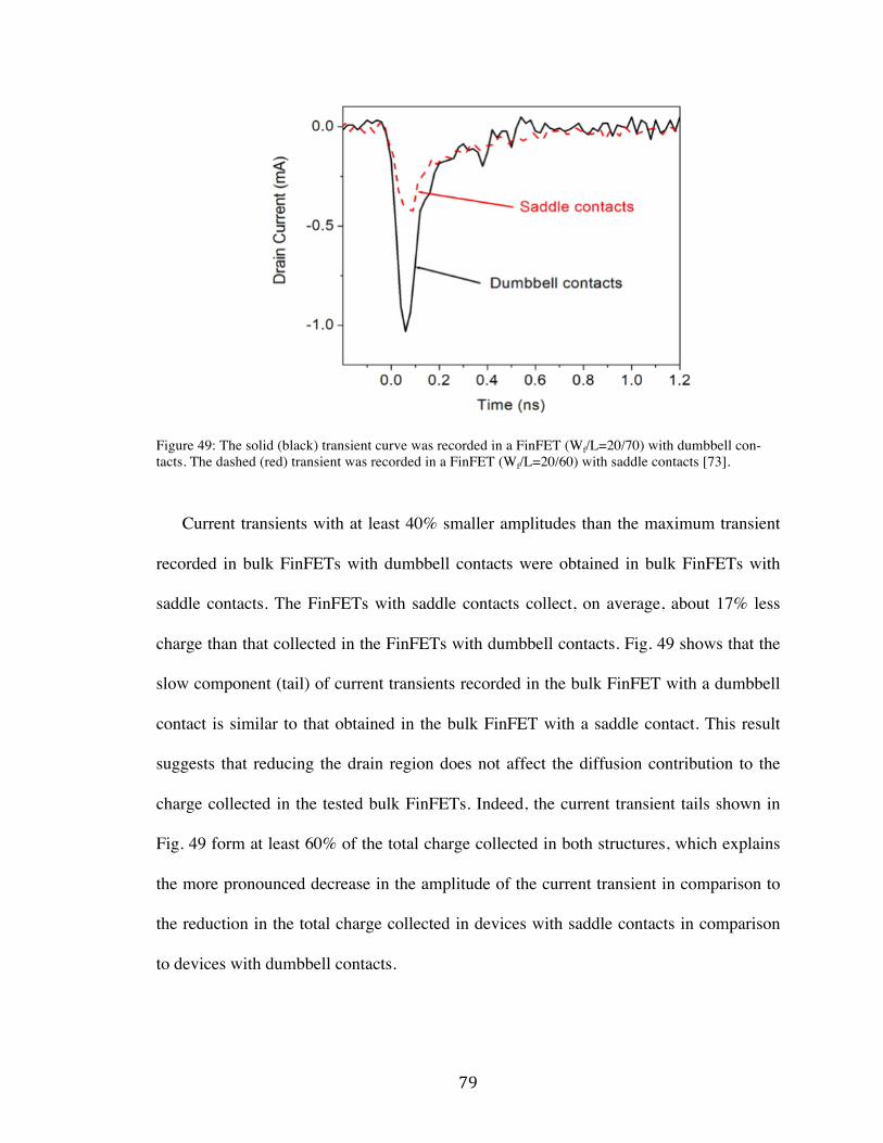
79
Figure 49: The solid (black) transient curve was recorded in a FinFET (Wf/L=20/70) with dumbbell con-tacts. The dashed (red) transient was recorded in a FinFET (Wf/L=20/60) with saddle contacts [73].
Current transients with at least 40% smaller amplitudes than the maximum transient
recorded in bulk FinFETs with dumbbell contacts were obtained in bulk FinFETs with
saddle contacts. The FinFETs with saddle contacts collect, on average, about 17% less
charge than that collected in the FinFETs with dumbbell contacts. Fig. 49 shows that the
slow component (tail) of current transients recorded in the bulk FinFET with a dumbbell
contact is similar to that obtained in the bulk FinFET with a saddle contact. This result
suggests that reducing the drain region does not affect the diffusion contribution to the
charge collected in the tested bulk FinFETs. Indeed, the current transient tails shown in
Fig. 49 form at least 60% of the total charge collected in both structures, which explains
the more pronounced decrease in the amplitude of the current transient in comparison to
the reduction in the total charge collected in devices with saddle contacts in comparison
to devices with dumbbell contacts.

80
This difference in the collected charge values is significant for recent generation
technologies where the critical charge is on the order of 1-10 fC [74]. Integration of the
transients in Fig. 49 over time to obtain the collected charge results in at least six times
more charge than that generated in the fin (18 fC) in both structures. In order to investi-
gate this amplification effect in bulk FinFETs, the drain, source and well currents are re-
ported for TRIBICC testing later in this chapter.
6.1.2. SOI FinFETs
6.1.2.1. Substrate-bias-dependence of the transient response of SOI FinFETs with saddle
contacts
Similar to SOI FinFETs with dumbbell contacts, the transient response of SOI Fin-
FETs with saddle contacts demonstrated a strong dependence on the substrate bias during
irradiation. A large amount of charge is collected in the substrate when negatively biased
(-5V). This effect is significantly mitigated when the substrate is biased positively (+5
V); the corresponding figure is not shown since no charge was collected for this particu-
lar SOI FinFET. Plotted in Fig. 50 are the values of charge collected (fC) along the x-axis
(along the gate) in the substrate source and drain terminals. There was no charge collect-
ed in the gate in this device. The SOI FinFET was biased in the off state configuration
with a drain bias of 1 V, a substrate bias of -5 V and all other terminals grounded. The
obtained result in Fig. 50 suggests that SOI FinFETs with saddle contacts are vulnerable
to the capacitive coupling observed first in devices with dumbbell contacts.
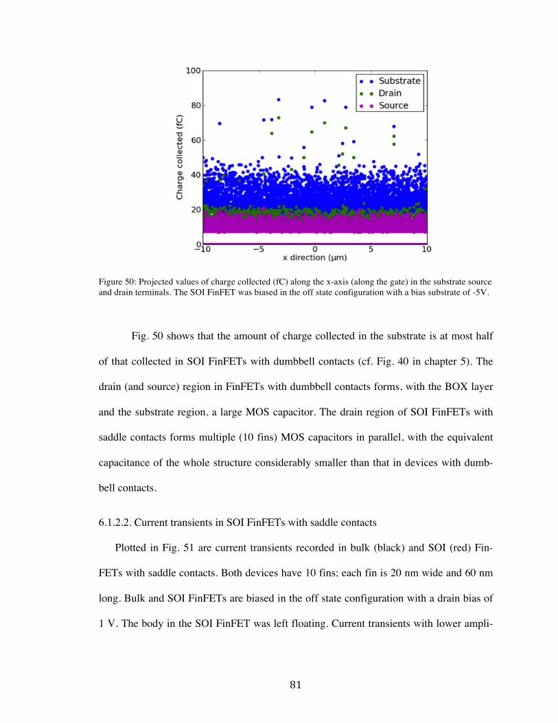
81
Figure 50: Projected values of charge collected (fC) along the x-axis (along the gate) in the substrate source and drain terminals. The SOI FinFET was biased in the off state configuration with a bias substrate of -5V.
Fig. 50 shows that the amount of charge collected in the substrate is at most half
of that collected in SOI FinFETs with dumbbell contacts (cf. Fig. 40 in chapter 5). The
drain (and source) region in FinFETs with dumbbell contacts forms, with the BOX layer
and the substrate region, a large MOS capacitor. The drain region of SOI FinFETs with
saddle contacts forms multiple (10 fins) MOS capacitors in parallel, with the equivalent
capacitance of the whole structure considerably smaller than that in devices with dumb-
bell contacts.
6.1.2.2. Current transients in SOI FinFETs with saddle contacts
Plotted in Fig. 51 are current transients recorded in bulk (black) and SOI (red) Fin-
FETs with saddle contacts. Both devices have 10 fins; each fin is 20 nm wide and 60 nm
long. Bulk and SOI FinFETs are biased in the off state configuration with a drain bias of
1 V. The body in the SOI FinFET was left floating. Current transients with lower ampli-

82
tude, smaller FWHM, and negligible tails were recorded in SOI FinFETs with saddle
contacts.
Figure 51: Current transients recorded in bulk and SOI FinFETs with saddle contacts. Both devices have 10 fins; each fin is 20 nm wide and 60 nm long. Both devices were biased in the off state configuration with a drain bias of 1 V. The body of the SOI FinFET was left floating.
Fig. 51 shows that FWHM as small as 50 ps is obtained in the SOI FinFETs. The bur-
ied oxide in the SOI FinFETs isolates the fin (active region) from the substrate, eliminat-
ing the diffusion component in the drain current transient. This explains the absence of
the tail and the lower amplitude in the current transient recorded in SOI FinFET. Integrat-
ing over time the current transients shown in Fig. 51 shows that the tested bulk FinFETs
collects about 8 times more charge than that collected in the evaluated SOI FinFETs.
Similarly to conventional SOI FinFETs with dumbbell contacts, SOI devices with saddle
contacts exhibit considerably higher tolerance to SEEs in comparison to their bulk coun-
terparts.

83
Similar SOI FinFET to the one tested above (cf. Fig. 51) was simulated using TCAD
simulation tool. The simulated drain current transient is shown in Fig. 52. Fig. 52 shows
that the simulated drain current transient is about 5 times faster than that recorded exper-
imentally (cf. Fig. 51).
Figure 52: Simulated drain current transient in an SOI FinFET. A FWHM of 13 ps is obtained.
The measured FWHM (50 ps) is comparable to the resolution of the 20 GHz scope
(~20 ps) used in the TRIBICC experiments. Moreover, parasitic components present in
the measurement set up of fast SEE transients [75] appeared to significantly modulate the
shape of the recorded transient [76]. In fact, Current transients with FWHM of as small as
2 ps were simulated in SOI FinFET by Turowski et al using CFDRC mixed CAD tools
[76]. These results suggest that the recorded current transients in SOI FinFETs are more
likely to be shorter than what can be measured experimentally.

84
6.2. Transient shunt effect in FinFETs with saddle contacts
6.2.1. Bulk FinFETs with saddle contacts
Fig. 53 shows the current transients recorded at the drain, source and well terminals in
a bulk FinFET with saddle contacts. The device was biased in the OFF state configura-
tion during irradiation with a drain bias of 1 V and all other terminals grounded. Fig. 53
shows that prompt current transients with opposite signs were obtained in the drain and
source terminals. This results from the formation of a transient conductive path in the
FinFET body. When the heavy ion passes between the two neighboring junctions, the
plasma track of the ion temporarily provides a shunt path [48][77] between the source
and drain. The source-well and drain-well junctions are 60 nm apart in the tested FinFET,
which is comparable to the radius of the ion track, enabling a lateral shunt.
The generated carriers in the fin are accelerated toward the drain terminal due to the bias,
producing the drain and source current transients illustrated in Fig. 53. The drain current
transient in Fig. 53 exhibits slightly higher amplitude with a significantly longer tail than
the source current transient.
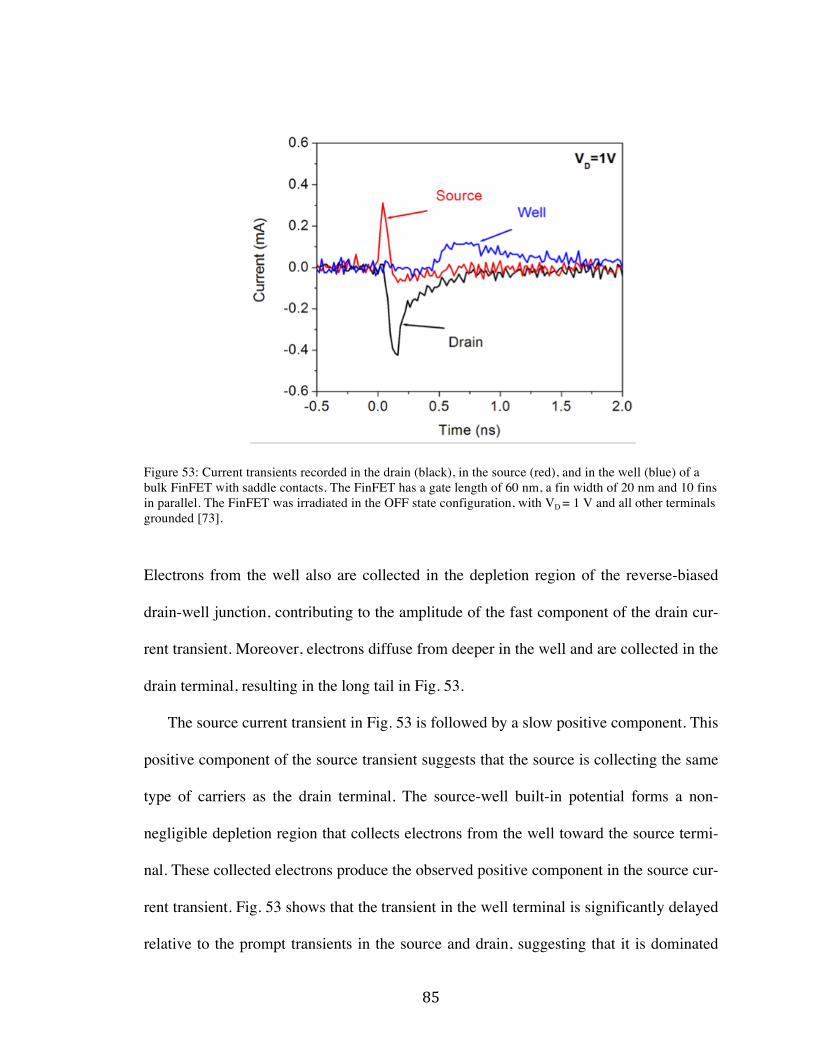
85
Figure 53: Current transients recorded in the drain (black), in the source (red), and in the well (blue) of a bulk FinFET with saddle contacts. The FinFET has a gate length of 60 nm, a fin width of 20 nm and 10 fins in parallel. The FinFET was irradiated in the OFF state configuration, with VD = 1 V and all other terminals grounded [73].
Electrons from the well also are collected in the depletion region of the reverse-biased
drain-well junction, contributing to the amplitude of the fast component of the drain cur-
rent transient. Moreover, electrons diffuse from deeper in the well and are collected in the
drain terminal, resulting in the long tail in Fig. 53.
The source current transient in Fig. 53 is followed by a slow positive component. This
positive component of the source transient suggests that the source is collecting the same
type of carriers as the drain terminal. The source-well built-in potential forms a non-
negligible depletion region that collects electrons from the well toward the source termi-
nal. These collected electrons produce the observed positive component in the source cur-
rent transient. Fig. 53 shows that the transient in the well terminal is significantly delayed
relative to the prompt transients in the source and drain, suggesting that it is dominated
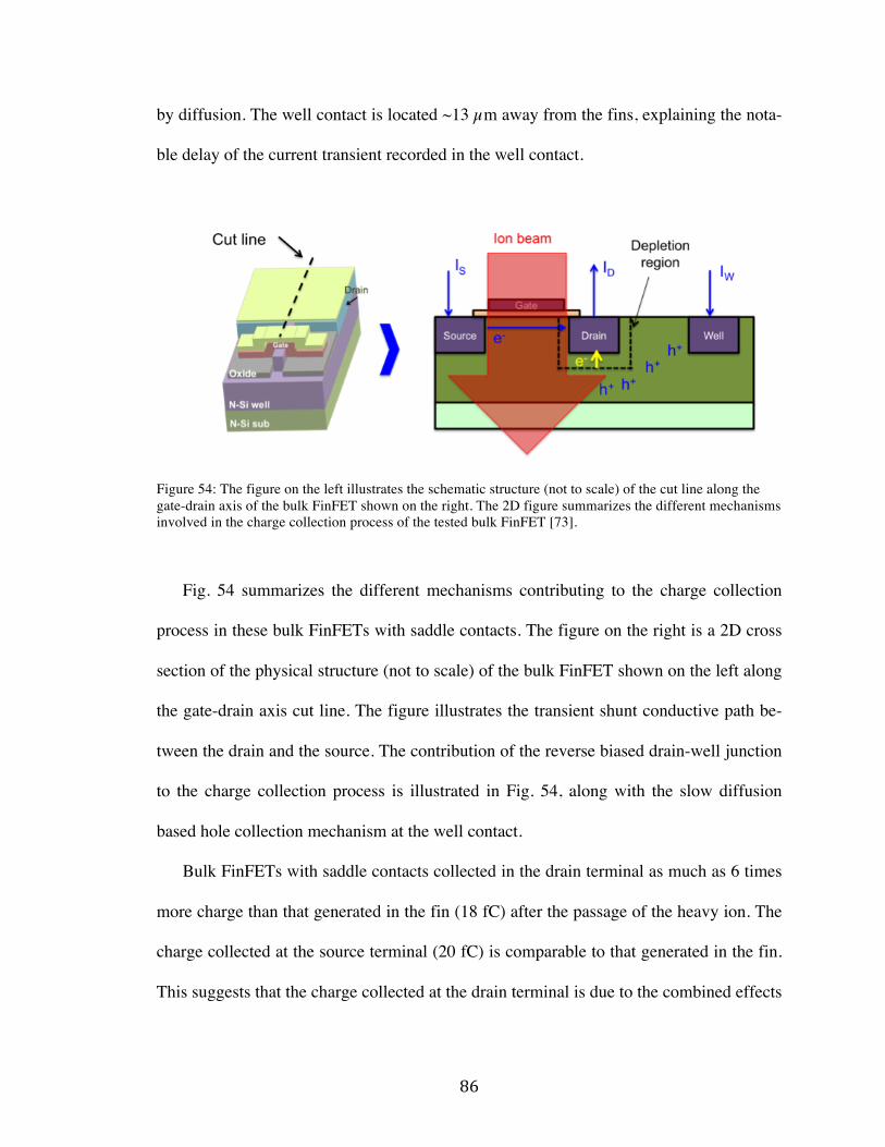
86
by diffusion. The well contact is located ~13 µm away from the fins, explaining the nota-
ble delay of the current transient recorded in the well contact.
Figure 54: The figure on the left illustrates the schematic structure (not to scale) of the cut line along the gate-drain axis of the bulk FinFET shown on the right. The 2D figure summarizes the different mechanisms involved in the charge collection process of the tested bulk FinFET [73].
Fig. 54 summarizes the different mechanisms contributing to the charge collection
process in these bulk FinFETs with saddle contacts. The figure on the right is a 2D cross
section of the physical structure (not to scale) of the bulk FinFET shown on the left along
the gate-drain axis cut line. The figure illustrates the transient shunt conductive path be-
tween the drain and the source. The contribution of the reverse biased drain-well junction
to the charge collection process is illustrated in Fig. 54, along with the slow diffusion
based hole collection mechanism at the well contact.
Bulk FinFETs with saddle contacts collected in the drain terminal as much as 6 times
more charge than that generated in the fin (18 fC) after the passage of the heavy ion. The
charge collected at the source terminal (20 fC) is comparable to that generated in the fin.
This suggests that the charge collected at the drain terminal is due to the combined effects

87
of both shunt collection and drain-substrate interaction with the latter effect contributing
by about 80 % to the total charge collected at the drain terminal of bulk FinFETs.
6.2.2. SOI FinFETs with saddle contacts
Figure 55 shows the current transients in the drain, source, and substrate terminals of
an SOI FinFET biased in the OFF state configuration with a drain bias of 1 V and all oth-
er terminals grounded.
Figure 55: Current transients recorded in the drain (black), in the source (red), and in the well (blue) of an SOI FinFET with saddle contacts. The FinFET has a gate length of 60 nm, a fin width of 20 nm and 10 fins in parallel. The FinFET was irradiated in the OFF state configuration, with VD = 2 V and all other terminals grounded [73].
Similar to the bulk FinFETs, SOI FinFETs exhibit current transients representing cur-
rent flow from drain to source. However, in the SOI FinFETs, the amplitude of both cur-
rent transients is the same, and no diffusion component is obtained in the drain current
transient. The buried oxide in the SOI FinFETs isolates the fin from the well, which elim-

88
inates the diffusion component in the drain current transient; so only the shunt effect
leads to a measurable transient. On the other hand, the 46 MeV incident copper ion cross-
es the fin with a speed of 1.18 × 10⁷ m/s. The ion’s velocity is calculated using the kinetic
energy formula below:
! =12× m × !
!, (9)
where E is the ion’s energy, m is the ion’s mass and v is the ion’s velocity. The ion
spends about 5 fs in the 65 nm fin. This value (5 fs) is much smaller than the obtained
FWHM of the SOI FinFET (~50 ps). Heavy ion induced carriers in the fin may take more
time to get collected due to the floating body effects in the SOI FinFET.
6.3. Drain bias dependence of the shunt effect in FinFETs with saddle contacts
6.3.1. Bulk FinFETs with saddle contacts
Current transients recorded in bulk FinFETs demonstrate a strong drain bias depend-
ence when increasing the drain voltage during irradiation. The bulk FinFETs investigated
in the previous paragraph (cf. Fig. 50) were tested under the same conditions with a high-
er drain bias (2 V).

89
Figure 56: Current transients recorded in the drain (black), in the source (red), and in the well (blue) of a bulk FinFET with saddle contacts. The FinFET has a gate length of 60 nm, a fin width of 20 nm and 10 fins in parallel. The FinFET was irradiated in the OFF state configuration, with VD = 2 V and all other terminals grounded [73].
Plotted in Fig. 56 are current transients recorded in the drain (black), in the source
(red), and in the well (blue) of a bulk FinFET with saddle contacts biased in the off state
configuration with a drain bias of 2 V. Increasing the drain bias to 2 V increases the am-
plitudes of both the drain and source current transients. Comparing the current transients
in Fig. 56 to those shown in Fig. 53, it can be observed that the amplitude of the drain and
source current transients increased by about 200 µA. Thus, an increase of 66% in the am-
plitude of drain and source current transients is obtained for bulk devices. This increase
in the amplitudes of the source and drain current transients is consistent with the conduc-
tive nature of the transient shunt path formed along the FinFET channel.
Integrating the drain current transients in Figs. 53 and 56 demonstrates that increas-
ing the drain bias of these bulk FinFETs modifies the shape of the recorded transients but
not the total collected charge. The charge collected at the drain terminal at high drain bias
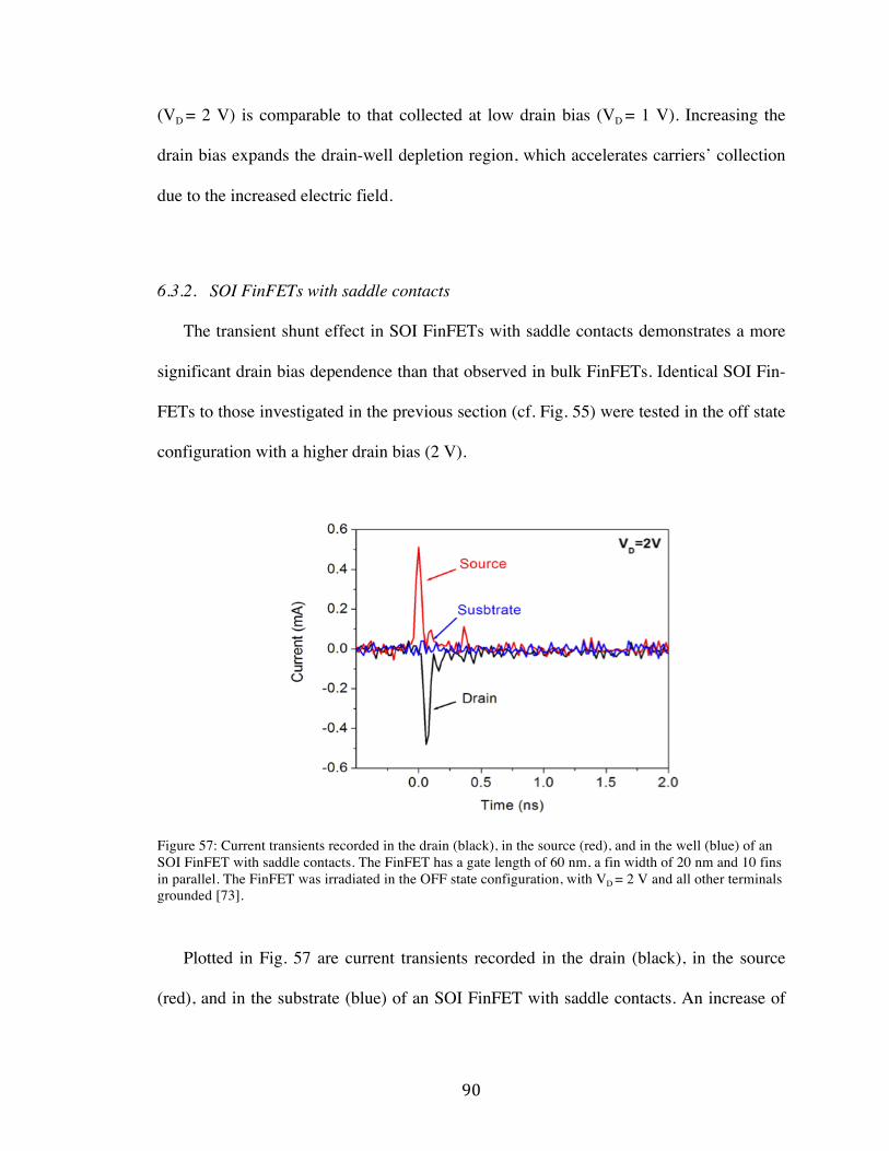
90
(VD = 2 V) is comparable to that collected at low drain bias (VD = 1 V). Increasing the
drain bias expands the drain-well depletion region, which accelerates carriers’ collection
due to the increased electric field.
6.3.2. SOI FinFETs with saddle contacts
The transient shunt effect in SOI FinFETs with saddle contacts demonstrates a more
significant drain bias dependence than that observed in bulk FinFETs. Identical SOI Fin-
FETs to those investigated in the previous section (cf. Fig. 55) were tested in the off state
configuration with a higher drain bias (2 V).
Figure 57: Current transients recorded in the drain (black), in the source (red), and in the well (blue) of an SOI FinFET with saddle contacts. The FinFET has a gate length of 60 nm, a fin width of 20 nm and 10 fins in parallel. The FinFET was irradiated in the OFF state configuration, with VD = 2 V and all other terminals grounded [73].
Plotted in Fig. 57 are current transients recorded in the drain (black), in the source
(red), and in the substrate (blue) of an SOI FinFET with saddle contacts. An increase of

91
300 µA in the amplitudes of the drain and source current transients is obtained in SOI
FinFETs when increasing the drain bias to 2 V during irradiation. An increase of 150% in
the amplitude of the current transient is observed. This augmentation of the transient am-
plitudes is ~2.3 times bigger than that exhibited by the bulk FinFETs (cf. Figs. 53 and
56). The increased drain bias in SOI FinFETs is entirely dropped in the channel region,
enhancing the resistive nature of shunt effect. In bulk FinFETs the increased drain bias is
partially dropped in the drain-well junction enhancing both the amplitude and the slow
component (tail) of the drain current transients.
Charge collected in the drain terminals of SOI FinFET is equal to that collected in the
source terminal. This charge (38 fC) is about two times larger than that generated in a
single fin (18 fC). The obtained charge enhancement effect is most likely due to the bipo-
lar amplification originated from the floating body effects observed first at lower drain
bias (1 V).
The obtained charge enhancement can also be explained by the onset of the shunt ef-
fect in more than one fin, resulting in the high amounts of charge collected in SOI Fin-
FETs, exceeding the total charge generated in a single fin. In support of this interpreta-
tion, the fin-to-fin pitch in the investigated SOI FinFETs is 200 nm. The high-density
(>1018 cm-3) heavy ion track is demonstrated through TCAD simulations to expand over
200 nm, which supports the contribution of the neighboring fins to the struck fin to the
observed charge collection.
This chapter shines light on some of the very challenging scaling impacts on the ad-
vanced devices’ electrical behavior. Semiconductor devices are continuously shrinking at
a furious pace thanks to the achieved breakthroughs in both the technology and the de-

92
vice’s design. Technology scaling affects the radiation response of the semiconductor de-
vices. The devices have comparable dimensions to those of the ion beam. The ion semi-
conductor interaction needs to be reviewed for extremely small feature sizes. New effects
are more likely to govern the radiation response of highly scaled devices, in particular for
the next FinFET generations. For instance, the shunt effect appears to play a key role in
the charge collection of state of the art bulk and SOI FinFETs with the highest amounts
of charge collected obtained in bulk technology.
93
CHAPTER VII
CONCLUSION
This thesis describes new results related to the transient radiation response of both
large and state of the art bulk and SOI FinFETs. It provides one of the first detailed char-
acterizations of the transient-radiation response of highly scaled FinFETs. The drain re-
gion in bulk FinFETs is demonstrated, through TPA experiments, to dominate the charge
collection process in these structures, masking the intrinsic contribution of the fins. This
result was validated via IBICC experiments on sub-70 nm bulk FinFET with fin width as
small as 5 nm. The sensitive region of bulk FinFETs corresponds to the drain region of
these structures. FinFET scaling is focused on the fin region. The drain-well junction of
FinFET devices in general (bulk and SOI) enhances the collection volume throughout fin-
drain region, especially for devices with conventional drain regions (dumbbell contacts).
This result is interesting for FinFET-based circuits where drain (and source) region are
sufficiently big to collect enough charge to upset the cell. Bulk FinFETs with reduced
drain regions (individual saddle contacts) demonstrated sensitive regions that map fairly
well to the drain region. The amount of charge collected in bulk FinFETs with saddle
contacts, however, is at least 17% less than that collected in bulk FinFETs with dumbbell
contacts. This result is extremely important when values of critical charge are on the or-
der of 1-10 fC. The results of this work suggest that improving the drain region design of
bulk FinFETs will contribute a great deal into ameliorating the SEE tolerance of bulk
FinFET devices.

94
Charge collection in SOI FinFETs with dumbbell contacts showed a strong depend-
ence on the substrate bias, with the highest amount of charge collected when the substrate
is negatively biased (~140 fC). The depletion region underneath the BOX in SOI struc-
tures leads to charge separation in the substrate of SOI devices, inducing charge to be col-
lected in the drain (and the source) via capacitive coupling. The substrate effect modu-
lates the charge collection of SOI FinFETs even when the substrate is grounded. SOI
FinFETs with saddle contacts demonstrated similar substrate bias dependences with 2
times lower amounts of charge collected in the substrate and the drain terminals. The re-
sults obtained from SOI devices suggest that the substrate needs to be appropriately bi-
ased (positively) to eliminate charge collection in the substrate. This effect can decrease
the SEE tolerance of SOI devices.
Current transients were recorded for the first time in highly scaled bulk and SOI Fin-
FETs with FWHM values of as low as 75 ps and 50 ps, respectively. These extremely
short pulses were captured using a high speed test set, including a 20 GHz single shot
scope. Charge enhancement was observed in bulk FinFETs with dumbbell contacts col-
lecting as much as 8 times more charge than that generated in the fin. Comparable
amount of charge amplification (x6) was observed in bulk FinFETs with saddle contacts.
Charge enhancement in SOI FinFETs with saddle contacts is obtained at high drain bias-
es (2 V). The observed charge enhancement effect in SOI FinFETs may be the result of
the combined effects of the bipolar amplification in the FinFET and the onset of the shunt
effect in the neighboring fins to the struck fin. Shunt effect, plays a key role in the charge
collection process in the investigated bulk and SOI FinFETs. The extremely small de-
vice’s feature size allows the ion truck to affect the whole channel area, which promotes
95
the transient shunt collection. This illustrates the future challenges to experimentally
identify the sensitive nodes in the next generations of extremely scaled FinFETs. The
shunt effect demonstrated a strong drain bias dependence, which supports the conductive
nature of the transient shunt path. Shunt collection includes charge generated from the ion
semiconductor interaction as well as from other charge originating from the external cir-
cuit. This illustrates one aspect of the complexity to investigate the critical charge param-
eter in FinFET-based structures.
SOI FinFETs exhibit shorter current transients with negligible tails and considerably
smaller collected charge in comparison to bulk FinFETs. Highly scaled bulk FinFETs
demonstrated higher SEE tolerance than that of bulk FinFETs. However, the results in
this thesis suggest that bulk FinFETs with improved designs of the drain region will make
a competitive product with comparable SEE tolerance to that of SOI FinFETs.
96
REFERENCES
[1] D. Hisamoto, W. C. Lee, J. Kedzierski, H. Takeuchi, K. Asano, C. Kuo, E. Anderson, T. J. King, J. Bokor, and C. Hu, “FinFET—A Self-Aligned Double-Gate MOSFET Scalable to 20 nm,” IEEE Trans. Electron Dev., vol. 47, no. 12, pp. 2320 - 2325, 2000.
[2] [Online]. http://newsroom.intel.com/community/intel_newsroom/blog/2011/05/04/intel-reinvents-
transistors-using-new-3-d-structure. [3] [Online]. http://www.eetimes.com/electronicsnews/4213622/TSMC-to make-FinFETs-in 450-mm-fab [4] [Online]. Available: http://www.eetimes.com/electronics-news/4215729/Intel-to-use-tri-gate-
transistors-at-22-nm [5] F. El-Mamouni, E. X. Zhang, R. D. Schrimpf, D. M. Fleetwood, R. A. Reed, S. Cristoloveanu, and
W. Xiong “Fin-Width Dependence of Ionizing Radiation-Induced Subthreshold-Swing Degradation in 100-nm-Gate-Length FinFETs,” IEEE Trans. Nucl. Sci., vol. 56, no. 6, pp. 3250-3255, 2009.
[6] M. Gaillardin, P. Paillet, V. Ferlet-Cavrois, S. Cristoloveanu, O. Faynot, and C. Jahan, “High Toler-
ance to Total Ionizing Dose of Omega-Shaped Gate Field-Effect Transistors,” Appl. Phys. Lett., vol. 88, no. 22, pp. 2235111–2235113, 2006.
[7] M. Gaillardin, P. Paillet, V. Ferlet-Cavrois, O. Faynot, C. Jahan, and S. Cristoloveanu, “Total Ionizing
Dose Effects on Triple-Gate FETs,” IEEE Trans. Nucl. Sci., vol. 53, no. 6, pp. 3158-3165, 2006. [8] S. Put, E. Simoen, M. Jurczak, M. V. Uffelen, P. Leroux, and C. Claeys, “Influence of Fin Width on
the Total Dose Behavior of p-Channel Bulk MuGFETs.” IEEE Trans. Nucl. Sci., vol. 31, no. 3, pp. 243-245, 2010.
[9] G. E. Moore, “Cramming More Components Onto Integrated Circuits,” Electronics, vol. 38, no. 8, pp.
82-85, 1965. [10] R. S. Muller, T. I. Kamins, and M. Chan, “Device Electronics for Integrated Circuits,” John Wiley and
sons, 2003. [11] D. J. Frank, R. H. Dennard, E. Nowak, P. M. Solomon, Y. Taur, and H. P. Wong, “Device Scaling
Limits of Si MOSFETs and Their Application Dependencies,” Proceedings of the IEEE, vol. 89, no. 3, pp. 259 - 288 2001 (invited paper).
[12] F. El-Mamouni, E. X. Zhang, N. D. Pate, N. Hooten, R. D. Schrimpf, R. A. Reed, K. F. Galloway, D.
McMorrow, J. Warner, E. Simoen, C. Claeys, A. Griffoni, D. Linten, and G. Vizkelethy, “Laser- and Heavy Ion-Induced Charge Collection in Bulk FinFETs,” IEEE Trans. Nucl. Sci., vol. 58, no. 6, pp. 2563-2569, 2011.
[13] J. P. Colinge, “FinFETs and Other Multi-Gate Transistors,” Springer, 2007.
[14] T. C. May and M. H. Woods, “A New Physical Mechanism for Soft Errors in Dynamic Memories,” Proceedings 16 Int’l Reliability Physics Symposium, pp. 33-40, 1978.
[15] J. N. Lin, K. C. Chan, C. Y. Chen, and M. H. Chiang, “Discrete Impurity Dopant Fluctuation in Mul-
ti-Fin FinFFTs: 3D Simulation-Based Study,” Proceedings of Electron Devices and Solid-State Cir-
97
cuits, pp. 577-580, 2007. [16] B. Yu, L. Chang, S. Ahmed, H. Wang, S. Bell, C. Y. Yang, C. Tabery, C. Ho, Q. Xiang, T. J. King, J.
Bokor, C. Hu, M. R. Lin, and D. Kyser, “FinFET Scaling to 10 nm Gate Length,” Proceedings of In-ternational Electron Devices Meeting, 2002.
[17] T. Chiarella, L. Witters, A. Mercha, C. Kerner, R. Dittrich, M. Rakowski, C. Ortolland, L. A. Rag-
narsson, B. Parvais, A. De Keersgieter, S. Kubicek, A. Redolfi, R. Rooyackers, C. Vrancken, S. Brus, A. Lauwers, P. Absil, S. Biesemans and T. Hoffmann, “Migrating from Planar to FinFET for Further CMOS Scaling: SOI or Bulk?,” Proceedings of ESSDERC, pp. 85-88, 2009.
[18] C. Barillot and P. Calvel, “Review of Commercial Spacecraft Anomalies and Single-Event-Effect Oc-
currences,” IEEE Trans. Nucl. Sci., vo. 43, no. 2, pp. 453-460, 1996. [19] D. Binder, E. C. Smith, and A. B. Holman, “Satellite Anomalies from Galactic Cosmic Rays,” IEEE
Trans. Nucl. Sci., vol. 22, no. 6, pp. 2675-2680, 1975. [20] J. F. Ziegler and W. A. Lanford, "Effect of Cosmic Rays on Computer Memories", Science, vol. 206,
no. 4420, pp. 776-788, 1979. [21] [Online]. http://www.intechopen.com/books/advances-in-solid-state-circuit-technologies/dimension-
increase-in-metal-oxide-semiconductor-memories-and-transistors [22] G. R. Rao and J. Hewkin, “64-K dynamic RAM needs only one 5-Volt supply to outstrip 16-K parts,”
Electronics, vol. 5, no. 20, pp. 109-116, 1978. [23] R. C. Varshney and K. Venkatataswaran, “A block organized 64-kbit CCD memory,” IEEE J. Solid
State Circuits, vol. 13, no. 5, pp. 681-687, 1978. [24] L. Massengill, “SEU Modeling and Prediction Technique”, NSREC short course, 1993. [25] S. Hayakawa, Cosmic Ray Physics: Nuclear and Astrophysical Aspects (Physics & Astronomical
Monograph), John Wiley & Sons, 1970. [26] A. W. Wolfendale, Cosmic Rays at Ground Level, Institute of Physics, 1973. [27] [Online]. http://physics.about.com/od/physicsmtop/g/muon.htm [28] [Online]. http://cosmic.lbl.gov/SKliewer/Cosmic_Rays/Muons.htm [29] J. R. Letaw and E. Normand, “Guidelines for Predicting Single-Event Upset in Neutron Environ-
ments,” IEEE Trans. Nucl. Sci., vol. 38, no. 6, pp. 1500-1506, 1991. [30] C. S. Guenzer, E. A. Wolicki, and R. G. Allas, “Single Event Upset of Dynamic RAMs by Neutrons
and Protons,” IEEE Trans. Nucl. Sci., vol. 26, no. 6, pp. 5048 - 5052, 1979. [31] [Online]. holbert.faculty.asu.edu/eee560/RadiationEffectsDamage.pdf [32] D. Filges and F. Goldenbaum, Handbook of Spallation Research: Theory, Experiments and Applica-
tions, Wiley, 2009. [33] S. Buchner, N. Kanyogoro, D. McMorrow, C. C. Foster, P. M. O’Neill, and K. V. Nguyen, “Variable
Depth Bragg Peak Method for Single Event Effects Testing,” IEEE Trans. Nucl. Sci., vol. 58, no. 6, pp. 2976-2982, 2011.
[34] T. R. Oldham, “Ionizing Radiation Effects in MOS Oxides”, World Scientific Pub, 2000.

98
[35] G. Jaffe,” Zur theorie der ionisation in kilonnen,” Ann. Phys. (Leipzig), vol. 42, p. 303, 1913. [36] L. Onsager, “Initial recombination of ions”, Physical Review, vol. 54, p. 554, 1938. [37] J. R. Srour, O. L. Curtis, Jr., and K. Y. Chiu, “Charge Transport Studies in SiO2: Processing Effects
and Implications for Radiation Hardening,” IEEE Trans. Nucl. Sci, vol. 21, pp. 73-80, 1974. [38] F. Saigne, “Une Nouvelle Approche de la Selection des Composants de Type MOS Dans
l’Envirenement Radiatif Spatial”, Ph.D dissertation, 1998. [39] J. R. Schwank, V. Ferlet-Cavrois, M. R. Shaneyfelt, P. Paillet, and P. E. Dodd, “Radiation Effects in
SOI Technologies,” IEEE Trans. Nucl. Sci., vol. 50, no. 3, pp. 522-538, 2003. [40] C. M. Hsieh, P. C. Murley, and R. R. O’Brien, “A field-funneling effect on the collection of alpha-
particle-generated carriers in silicon devices,” IEEE Electron Device Lett., vol. 2, no. 4, pp. 103-105, 1981.
[41] C. M. Hsieh, P. C. Murley, and R. R. O'Brien, “Collection of Charge from Alpha-Particle Tracks in
Silicon Devices,” IEEE Trans. Electron Dev., vol. 30, no. 6 , pp. 686-693, 1983. [42] S. Kirkpatrick, “Modeling Diffusion and Collection of Charge from Ionizing Radiation in Silicon De-
vices,” IEEE Trans. Electron Dev., vol. 26, no. 11, pp. 1742-1753, 1979. [43] V. Ferlet-Cavrois, G. Vizkelethy, P. Paillet, A. Torres, J. R. Schwank, M. R. Shaneyfelt J. Baggio, J.
du Port de Pontcharra, and L. Tosti, “Charge Enhancement Effect in NMOS Bulk Transistors Induced by Heavy Ion Irradiation—Comparison With SOI,” IEEE Trans. Nucl. Sci., vol. 51, no. 6, pp. 3255-3262, 2004.
[44] G. E. Davis, L.R. Hite, T. G. W. Blake, C. E. Chen, H.W. Lam, and R. DeMoyer, “Transient Radia-
tion Effects in SOI Memories,” IEEE Trans. Nucl. Sci., vol. 32, no. 6, pp. 4432–4437, 1985. [45] L. W. Massengill, D. V. Kerns, Jr., S. E. Kerns, and M. L. Alles, “Single Event Charge Enhancement
in SOI Devices,” IEEE Electron Dev. Lett., vol. 11, no. 2, pp. 98-99, 1990. [46] O. Musseau, V. Ferlet-Cavrois, A. B. Campbell, A. R. Knudson, W. J. Stapor, P. T. McDonald, J. L.
Pelloie, and C. Raynaud, “Charge Collection in Submicron CMOS/SOI Technology,” IEEE Trans. Nucl. Sci., vol. 44, no. 6, pp. 2124-2133, 1997.
[47] V. Ferlet-Cavrois, G. Gasiot, C. Marcandella, C. D’Hose, O. Flament, O. Faynot, J. du Port de Pont-
charra, and C. Raynaud, “Insights on the Transient Response of Fully and Partially Depleted SOI Technologies Under Heavy-Ion and Dose-Rate Irradiations,” IEEE Trans. Nucl. Sci., vo. 49, no. 6, pp. 2948-2956, 2002.
[48] J. R. Hauser, S. E. Diehl-Nagle, A. R. Knudson, A. B. Campbell, W. J. Stapor and P. Shapiro, “Ion
Track Shunt Effects in Multi-Junction Structures,” IEEE Trans. Nucl. Sci., vol. 32, no. 6, pp. 4115-4121, 1985.
[49] A. R. Knudson, A. B. Campbell, P. Shapiro, W. J. Stapor, E. A. Wolicki, E. L. Petersen, S. E. Diehl-
Nagle, J. Hauser, and P. V. Dressendorfer, “Charge Collection in Multilayer Structures,” IEEE Trans. Nucl. Sci., vol. 31, no. 6, pp. 1149-1154, 1984.
[50] V. Ferlet-Cavrois, P. Paillet, D. McMorrow, A. Torres, M. Gaillardin, J. S. Mellinger, A. R. Knuson,
A. B. Campbell, J. R. Schwank, G. Vizkelethy, M. R. Shanayfet, K. Hirose, O. Faynot, C. Jahan and L. Tosti, “Direct Measurement of Transient Pulses Induced by Laser and Heavy Ion Irradiation in De-ca-Nanometer Devices,” IEEE Trans. Nucl. Sci., vol. 52, no. 6, pp. 2104 - 2113 2005.
99
[51] P. E. Dodd, F. W. Sexton, G. L. Hash, M. R. Shaneyfelt, B. L. Draper, A. J. Farino, and R. S. Flores,
“Impact of Technology Trends on SEU in CMOS SRAMs,” IEEE Trans. Nucl. Sci., vol. 43, no. 6, pp. 2797-2804, 1996.
[52] P. Roche, J. M. Palau, G. Bruguier, C. Tavernier, R. Ecoffet, and J. Gasiot, “Determination of Key
Parameters for SEU Occurrence Using 3-D Full Cell SRAM Simulations,” IEEE Trans. Nucl. Sci., vol. 46, no. 6, pp. 1354-1362, 1999.
[53] J. P. Colinge, Silicon-On-Insulator Technology: Materials to VLSI. Boston: Kluwer Academic Pub-
lishers, 1997. [54] F. E. Mamouni, S. K. Dixit, R. D. Schrimpf, P. C. Adell, I. S. Esqueda, M. L. McLain, H. J. Barnaby,
S. Cristoloveanu, and W. Xiong, “Gate Length and Drain-Bias Dependence of Band-to-Band Tunnel-ing-Induced Drain Leakage in Irradiated Fully Depleted SOI Devices,” IEEE Trans. Nucl. Sci., vol. 55, no. 6, pp. 3259–3264, 2008.
[55] M. Gaillardin, P. Paillet, V. Ferlet-Cavrois, J. Baggio, D. McMorrow, O. Faynot, C. Jahan, L. Tosti,
and S. Cristoloveanu, “Transient Radiation Response of Single- and Multiple-Gate FD SOI Transis-tors,” IEEE Trans. Nucl. Sci., vo. 54, no. 6, pp. 2355-2362, 2007.
[56] D. McMorrow, V. Pouget, P. Fouillat, and S. Buchner, “Fundamentals of the Pulsed Laser Technique
for Single Event Effects Testing”, SERESSA, 2008. [57] C. Kittel, “Introduction to Solid State Physics,” Wiley, 1996. [58] J. S. Melinger, S. Buchner, D. McMorrow, W. J. Stapor, T. R. Weatherford, and A. B. Campbell,
“Critical Evaluation of the Pulsed Laser Method for Single Event Effects Testing and Fundamental Studies”, IEEE Trans. Nucl. Sci., vol. 41, no. 6, pp. 2574-2584, 1994.
[59] D. McMorrow, W. T. Lotshaw, J. S. Melinger, S. Buchner, and R. L. Pease, “Subbandgap Laser-
Induced Single Event Effects: Carrier Generation Via Two-Photon Absorbtion”, IEEE Trans. Nucl. Sci., vol. 49, no. 6, pp. 3002-3008, 2002.
[60] D. McMorrow, W. T. Lotshaw, J. S. Melinger, S. Buchner, J. D. Davis, R. K. Lawrence, J. H. Bow-
man, R. D. Brown, D. Carlton, J. Pena, J. Vasquez, N. Haddad, K. Warren, and L. Massengill, “Single Event Upset in Flip-Chip SRAM Induced by Through-Wafer, Two Photon Absorption”, IEEE Trans. Nucl. Sci. vol. 52, no. 6, pp. 2421-2425, 2005.
[61] B.L. Doyle, G. Vizkelethy, and D. S. Walsh, “Ion Beam Induced Charge Collection (IBICC) Studies
of Cadmium Zinc Telluride (CZT) Radiation Detectors,” Elsevier, vol. 161-163, pp. 457-461, 2000. [62] G. F. Knoll, “Radiation Detection and Measurement,” John Wiley and Sons, 1979. [63] N. A. Dodds, “Charge Generation by Secondary Particles from Nuclear Reactions in Back End of
Line Materials,” Masters thesis, Vanderbilt University, 2009. [64] D. McMorrow, J. S. Melinger, S. Buchner, T. Scott, R. D. Brown, and N. F. Haddad, “Application of
a pulsed laser for evaluation and optimization of SEU-hard design,” IEEE Trans. Nucl. Sci., vol. 47, no. 3, pp. 559–565, 2000.
[65] N. C. Hooten, “Characterization of the Two-Photon Absorption Carrier Generation Region in Bulk
Silicon Diodes,” Masters thesis, Vanderbilt University, 2011. [66] F. El-Mamouni, E. X. Zhang, R. D. Schrimpf, R. D. Reed, K. F. Galloway, D. McMorrow, E. Simoen,

100
C. Claeys, S. Cristoloveanu, and W. Xiong, “Pulsed laser-induced transient currents in bulk and sili-con-on-insulator FinFETs,” in Proc. IRPS, 2011, pp. 882–885.
[67] G. Vizkelethy, B. L. Doyle, D. K. Brice, P. E. Dodd, M. R. Shaneyfelt, and J. R. Schwank, “Radiation
Effects Microscopy for Failure Analysis of Microelectronic Devices,” Proceedings of the 9th Interna-tional Conference on Nuclear Microprobe Technology and Applications, vol. 231, no. 1–4, pp. 467–475, 2005.
[68] F. W. Sexton, K. M. Horn, B. L. Doyle, J. S. Laird, M. Cholewa, A. Saint, and G. J. F. Legge, “Rela-
tionship Between IBICC Imaging and SEU in CMOS ICs,” IEEE Trans. Nucl. Sci., vol. 40, no. 6, pp. 1787–1794, 1993.
[69] T. Chiarella, L. Witters, A. Mercha, C. Kerner, M. Rakowski, C. Ortolland, L. A. Ragnarsson, B. Par-
vais, A. D. Keersgieter, S. Kubicek, A. Redolfi, C. Vrancken, S. Brus, A. Lauwers, P. Absil, S. Biesemans, and T. Hoffmann, “Benchmarking SOI and bulk FinFET alternatives for planar CMOS scaling succession,” Solid-State Electron, vol. 54, no. 9, pp. 855–860, 2010.
[70] D. R. Ball, M. L. Alles, R. D. Schrimpf, S. Cristoloveanu, “Comparing Single Event Upset Sensitivity
of Bulk vs. SOI Based FinFET SRAM Cells using TCAD Simulations,” Proceedings of IEEE Interna-tional SOI Conference, pp. 1-2, 2012.
[71] J. R. Schwank, V. Ferlet-Cavrois, P. E. Dodd, M. R. Shaneyfelt, G. Vizkelethy, P. Paillet, and O.
Flament, “Analysis of Heavy-Ion Induced Charge Collection Mechanisms in SOI Circuits,” Solid-State Electronics, vol. 48, no. 6, pp. 1027–1044, 2004.
[72] G. Vizkelethy, D. K. Brice, and B. L. Doyle, “The Theory of Ion Beam Induced Charge in Metal-
Oxide Semiconductor Structures,” J. Appl. Phys, vol. 101, no. 7, pp. 0745061-0745066, 2007. [73] F. El-Mamouni, E. X. Zhang, D. R. Ball, B. Sierawski, M. P. King, R. D. Schrimpf, R. A. Reed, M. L.
Alles, D. M. Fleetwood, D. Linten, E. Simoen, G. Vizkelethy,” Heavy-Ion-Induced Current Transi-ents in Bulk and SOI FinFETs” accepted for possible publication in IEEE Trans. Nucl. Sci., 2012.
[74] D. McMorrow, J. Warner, S. DasGupta, V. Ramachandran, J. B. Boos, R. Reed, R. Schrimpf, P. Pail-
let, V. Ferlet-Cavrois, J. Baggio, S. Buchner, F. El-Mamouni, M. Raine, and O. Duhamel “Novel En-ergy-Dependent Effects Revealed in GeV Heavy Ion-Induced Transient Measurements of Antimony-Based III-V HEMTs,” IEEE Trans. Nucl. Sci., vol. 57, no. 6, pp. 3358-3368, 2010.
[75] M. Turowski, J. Pellish, K. Moen, A. Raman, J. Cressler, R. Reed, and G. Niu, “Reconciling 3-D
Mixed-Mode Simulations and Measured Single-Event Transients in SiGe HBTs,” IEEE Trans. on Nuclear Science, Dec. 2010
[76] M. Turowski, A. Raman, A. Fedoseyev, T. Bald, M. Alles, S. Ball, F. El-Mamouni, M. King, G.
Bersuker “Characterization and Mitigation of Radiation Effects in Nonplanar Nano-technology Mi-croelectronics”, DTRA Program Review, Vanderbilt Univ., May 2012.
[77] J.A. Zoutendyk, L.S. Smith, G. A. Soli, and R. Y. Lo, “Experimental Evidence For A New Single-
Event Upset (SEU) Mode in A CMOS SRAM Obtained From Model Verification,” IEEE Trans. Nucl. Sci. vol. 34, no. 6, pp. 1292-1299, 1987.

101