single-phase controlled rectifier...
TRANSCRIPT
3
Single-Phase Controlled RectifierCircuits
By the use of delayed triggering of a controlled rectifier the average and rmsload voltages in rectifier circuits can be smoothly adjusted.
3.1 SINGLE-PHASE CONTROLLED CIRCUITSWITH RESISTIVE LOAD
3.1.1 Voltage and Current Relations for a Half-Wave Controlled Rectifier
If the circuit of Fig. 3.1 is used with an arbitrary firing angle for the SCRswitch, the waveforms obtained are shown in Fig. 3.2 for half-wave operation. Theload voltage and current consist of pieces of sinusoid defined by the relationship
e t E tL mω ωπ πα π
( ) =+ α
sin, ,
, ,
3
2
…
… (3.1)
having an average value
E e t d tav L= ( )
= +( )
∫1
2
21
πω ω
πα
α
π
cosEm
(3.2)
Copyright 2004 by Marcel Dekker, Inc. All Rights Reserved.

Single-Phase Controlled Rectifier Circuits 53
FIG. 1 Single-phase, half-wave controlled rectifier circuit.
When 0, Eq. (3.2) reduces to Eq. (2.5b).The rms value EL of the load voltage in the circuit of Fig. 3.1 is obtained
by the use of eL (t) as follows
E e t d tL L2 21
2= ( )∫π
ω ωα
π
(3.3)
Therefore,
IE
R
E
RLL m= = −( ) + 2
1
22 2
ππ α αsin (3.4)
Combining Eqs. (3.2) and (3.4) gives a value for the ripple factor RF
FIG. 2 Load voltage waveform for single-phase, half-wave controlled rectifier circuitwith R load and 60.
Copyright 2004 by Marcel Dekker, Inc. All Rights Reserved.

Chapter 354
RFE
EL
av
=
−
2
1
=−( ) + ( )
+( )−
π π α α1 2 2
11
2
/ sin
cosα (3.5)
At 0, the ripple factor reduces to Eq. (2.8), having a value 1.21. When /2, the ripple factor increases to 1.98. Retardation of the switching angle asa means of controlling the average value of the load voltage therefore also resultsin the undesirable effect of increasing the rms value of the ac components.
The time average power dissipation in the load is found to be
P I R
E
R
L L
m
=
= −( ) +
2
2
4
1
22 2
ππ α αsin
(3.6)
The power factor PF of the single-phase, half-wave controlled rectifier circuitcan be obtained by combining Eqs. (3.1)(3.4), and (3.6):
PFP
E I
P
SL
s L
L
L
= =
=−( ) +1
2
2 2
2
π α απ
sin(3.7)
When 0, Eq. (3.7) reduces to 1/2 , which is the value for an uncontrolledrectifier in Eq. (2.27).
Fourier coefficients a1b1 for the fundamental or supply frequency compo-nent of the load voltage are found to be
a e t t d t
E t t d t
E
I
bI
L
m
m
= ( )
=
=
∫
∫
1
1α
πω ω ω
πω ω ω
cos
sin cos
πω ω ω
πe t t d tL0
21∫= ( ) sin
2αcos − 12π
π
2
2 π
0
(3.8)
Copyright 2004 by Marcel Dekker, Inc. All Rights Reserved.

Single-Phase Controlled Rectifier Circuits 55
=
=−( ) +
∫1
2
2 2
2
2
πω ω
π α απ
α
π
E t d t
E
m
m
sin
sin(3.9)
The peak value c1 of the fundamental load voltage is therefore
c a b
E
I
m
= +
= −( ) + −( ) +
12
12
2 2
42 1 2 2
πα π α αcos sin
(3.10)
Correspondingly, the time phase angle L1 between the sinusoidal supply voltageand the fundamental component of the load voltage (and current) is
ψ
απ α α
L
a
b1
1 1
1
1 2 1
2 2
=
= −−( ) +
−
−
tan
tancos
sin (3.11)
For 0 180 the phase angle is negative. In a linear, sinusoidal circuit anegative phase angle is associated with energy storage in a magnetic field. Butin the circuit of Fig. 3.1 no energy storage is possible. The delayed switchingcauses a phase lag of the fundamental current component which represents apower factor problem. The power factor reduction, however, is not attributableto an energy storage phenomenon and the instantaneous voltamperes remainspositive at all times, as in any resistive circuit. Nevertheless, it is found that someimprovement of power factor can be obtained by the connection of capacitanceacross the circuit terminals.
3.1.2 Power and Power Factor in Half-WaveRectifier Circuits
The load power can be written in the form of Eq. (2.25), using the subscript Lfor load
PL EsIL1 cos L1 (3.12)
Similarly, one can write an expression for the reactive voltamperes QL of thecontrolled load
QL EsIL1 sin L1 (3.13)
where
Copyright 2004 by Marcel Dekker, Inc. All Rights Reserved.
Chapter 356
Ic
L1
1
2=
(3.14)
EE
sm
2=
(3.15)
The apparent voltamperes SL at the circuit terminals is given by
SL EsIL (3.16)
But from Eqs. (3.12) and (3.13),
P Q E IL L s L2 2 2 2
1+ = (3.17)
It is found that (3.17) accounts for only part of the apparent voltamperes SL,given in Eq. (3.16).
The analytical difference between S2L and P2
LQ2L is sometimes expressed
in terms of the distortion or harmonic voltamperes DL.
S P Q DL L L L2 2 2 2= + + (3.18)
So that
D E I IL s L L= −2 2
1 (3.19)
The power factor of this circuit can also be expressed in terms of the currentdistortion factor IL1/IL and current displacement factor cos L1. In this case, how-ever, the expressions for distortion factor and displacement factor, in terms ofswitching-angle, do not offer any advantage over Eq. (3.7).
3.1.3 Capacitance Compensation of RectifierPower Factor
Consider operation of the circuit with a capacitor C across the supply terminals,Fig. 3.3. The instantaneous capacitor current is given by the continuous function
i t CE tc mω ω ω π( ) = +
sin2 (3.20)
The instantaneous load branch current is
i tE
RtL
mω ωπ πα π α
( ) =+
sin, ,
, ,
3
2
…
… (3.21)
By Kirchhoff’s law the instantaneous supply current is given by
Copyright 2004 by Marcel Dekker, Inc. All Rights Reserved.

Single-Phase Controlled Rectifier Circuits 57
FIG. 3 Single-phase, half-wave controlled rectifier circuit with supply side capacitance.
is (t) iL (t) ic (t) (3.22)
Because the load current and supply current are nonsinusoidal, the three branchcurrents cannot be described by phasor relationships. For the capacitor compen-sated circuit the real power PL, terminal voltage e(t), and the load branch currentiL (t) are unchanged, but the power factor PF is now a function of the rms valueof the supply current Is (not the load current IL).
PFP
E IL
s s
=(3.23)
In Fig. 3.3 the intention is that the power factor PF seen from the supply pointbe improved (i.e. increased) with respect to the uncompensated value PFL.
The rms supply current Is is given by
I i t d ts s2 2
0
21
2= ( )∫π
ω ωπ
(3.24)
Substituting (3.20–3.22) into (3.23) gives
IE
R
R
X
R
Xsm
c c
= + − +−( ) +
2
2 2 2 1
2
2 2
2
2
2
1 2
cos sin/
απ
π α απ (3.25)
The corresponding expression for power factor is then
PFR X R Xc c
=−( ) +
( ) + ( ) −( ) + −
1 2 2 2 2
2 2 2 1 2 22 2 2
/ sin /
/ / cos /
π α α π
α π π αα α π( ) + sin /2 2
( ) (3.26)
Copyright 2004 by Marcel Dekker, Inc. All Rights Reserved.

Chapter 358
Even if the value of C is adjusted continuously to give the best power factor forany fixed value of , the degree of power factor improvement realisable is onlyof the order of a few percent.
Maximization of the power factor can be achieved by minimization of therms supply current since PL is not affected by terminal capacitance. DifferentiatingEq. (3.25) with respect to C gives
dI
dC
E
RR C R R
X
R
Xs m
c c
= + −
+ − +−
24 2
2 1
22 2 2 1
2
22 22
2ω α
παπ
πcos cos αα απ
( ) +
−
sin2
2
21
(3.27)
For Is minimum, dIs/dC 0, which leads to the condition
1 1
2
1 2
2XC
Rc
= = −ω απ
cos(3.28)
With optimum capacitance the minimum value Ismin of Is that will supply thespecified load power is obtained by substituting the above expression for Xc intoEq. (3.25)
IE
R
R
Xsm
cmin
sin= − +
−( ) +
2
2 2 2
2
2
2
π α απ (3.29)
The optimum power factor PFmax is then given by
PFP
E IL
s smax
min
=(3.30)
3.1.4 Single-Phase Full-Wave Bridge RectifierCircuit
Full-wave, controlled rectification of the load voltage and current can be obtainedby use of the alternative configurations of Fig. 3.4 in which the controlled switchesare shown as thyristors. With a fixed value of switching angle and sinusoidalsupply voltage the load voltage waveform (Fig. 3.5) is defined by
e t E t E tL m mω ω πα
ω ππ
π α( ) = + −( )
+sin sin
2(3.31)
Copyright 2004 by Marcel Dekker, Inc. All Rights Reserved.

Single-Phase Controlled Rectifier Circuits 59
which has an average value twice as large as Eq. (3.2) for half-wave operation
EE
avm= +( )
πα1 cos (3.32)
When 0, Eq. (3.32) reduces to the value 2Em/ for a half sine wave. Therms value of the load current in the circuits of Fig. 3.4 is
IE
R Re t d t
E
R
Lm
L
m
= = ( )
= −( ) +
∫1
2
2
1
22 2
2
0
2
πω ω
ππ α α
π
sin (3.33)
FIG. 4 Single-phase, full-wave controlled rectifier circuits with R load.
Copyright 2004 by Marcel Dekker, Inc. All Rights Reserved.

Chapter 360
FIG. 5 Load voltage (and current) waveforms for single-phase, full-wave controlledrectifier with R load, 50.
The load current waveform (Fig. 3.5) has a ripple factor obtained by substitutingEqs. (3.32) and (3.33) into eq. (2.7)
I
IL
av
(3.34)
When 0, Eq. (3.34) reduces to the value RF 0.48, which was givenpreviously in Eq. (2.24) for uncontrolled operation.
Comparison of (3.33) with (3.4) shows that the rms value of the load currentwith full-wave rectification is 2 times the value for half-wave rectification, atany fixed firing angle. The average power dissipation in the load is given by
P P I R
E
R
s L
m
L
(3.35)
which is twice the value for corresponding half-wave operation.Operation of the rectifier circuits of Fig. 3.4 results in the supply current
waveform of Fig. 3.6, which is identical to the waveform for a single-phase acchopper circuit, discussed in Chapter 14. This waveform has zero average valueover any number of complete cycles and the supply current contains no dc oreven harmonic terms. The rms value Is of the supply current is
Copyright 2004 by Marcel Dekker, Inc. All Rights Reserved.
Single-Phase Controlled Rectifier Circuits 61
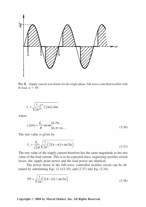
FIG. 6 Supply current waveforms for the single-phase, full-wave controlled rectifier withR load, 50.
I i t d ts = ( )∫1
2 0
2
πω ω
π2s
where
i tE
Rts
m( ) =+
ω ωπ πα π α
sin, ,
, ,
2 …
… (3.36)
The rms value is given by
IE
Rs
m= −( ) + 2
1
22 2
ππ α αsin
(3.37)
The rms value of the supply current therefore has the same magnitude as the rmsvalue of the load current. This is to be expected since, neglecting rectifier switchlosses, the supply point power and the load power are identical.
The power factor of the full-wave, controlled rectifier circuit can be ob-tained by substituting Eqs. (3.1)(3.35), and (3.37) into Eq. (3.16).
PF = −( ) + 1
22 2
ππ α αsin (3.38)
Copyright 2004 by Marcel Dekker, Inc. All Rights Reserved.
Chapter 362
At 0, the supply point power factor is unity since the supply current is thensinusoidal and in time phase with the supply voltage.
Comparison of Eqs. (3.35) to (3.38) shows that
PF P pu I pus s= ( ) = ( ) (3.39)
Expression (3.39) is true for any single-phase resistive circuit, irrespective ofwaveform, and therefore also applies to half-wave rectifier circuits, controlled oruncontrolled.
Because the supply voltage remains sinusoidal, the power factor of the full-wave controlled rectifier circuit may be interpreted as a product of displacementfactor and distortion factor. This involves calculation of the Fourier componentsa1b1, and c1 of the fundamental component is1 of the supply current.
a i t t d t
E
R
b i t d
s
m
s
I
I
= ( )
= −( )
= ( )
∫
∫
1
22 1
1
0
2
0
2
πω ω ω
πα
πω ω
π
π
cos
cos
sin tt(3.40)
= −( ) +
= +
E
R
c a b
m
22 2
12
12
ππ α αsin
I(3.41)
= −( ) + −( ) + E
Rm
22 1 2 2
2 2
πα π α αcos sin (3.42)
Coefficient c1, in (3.42), represents the peak value of the fundamental componentof the supply current. RMS supply current Is1 therefore has the value
Ic
s1
1
2= (3.43)
Combining Eqs. (3.18)(3.37)(3.42), and (3.43) gives a value for the current distor-tion factor
Current distortion factor =
=−( ) + −( ) +
I
Is
s
1
1
2
2 1 2 22
π
α π α αcos sin −( ) +
2
2 2π α αsin (3.44)
Copyright 2004 by Marcel Dekker, Inc. All Rights Reserved.

Single-Phase Controlled Rectifier Circuits 63
The displacement factor is given by
Current displacement factor =
=
=
=
−
cos
cos tan
ψs
a
b
b
c
1
1 1
1
1
1
2 ππ α α
α π α α
−( ) +
−( ) + −( ) +
sin
cos sin
2
2 1 2 22 2
(3.45)
At 0, both the current displacement factor and the current distortion factorare unity resulting in unity power factor, which compares with the correspondingvalue 1/2 for uncontrolled half-wave operation in Eq. (2.27). Displacementangle s1 between the supply voltage and the fundamental component of thesupply current becomes progressively more lagging as the switching angle isfurther retarded. The consequent displacement factor contribution to the progres-sively decreasing power factor can be compensated by the connection of shuntcapacitance at the circuit terminals. With resistive load the current distortionfactor and current displacement factor contribute roughly equal amounts to thecircuit power factor.
An alternative to the bridge converter for producing full-wave rectificationis the push–pull converter which uses a transformer with a centre-tapped second-ary winding, Fig. 3.7. This transformer has the same voltampere rating as theload. If the leakage inductance of the transformer is small, the load current andvoltage, with resistive load, have the form shown in Fig. 3.5. The equations ofSec. 3.1.3 also apply to this circuit if transformer losses are negligible. Wherean input transformer is required for isolation purposes the circuit of Fig. 3.7 isobviously applicable. If the requirement is to effectively increase the pulse orphase number from unity (as for single-phase, half-wave rectifiers) to two, thena bridge circuit of the type in Fig. 3.4 is likely to be cheaper.
FIG. 7 Single-phase, full-wave rectifier circuit using a center-tapped transformer.
Copyright 2004 by Marcel Dekker, Inc. All Rights Reserved.
Chapter 364
3.1.5 Worked Examples
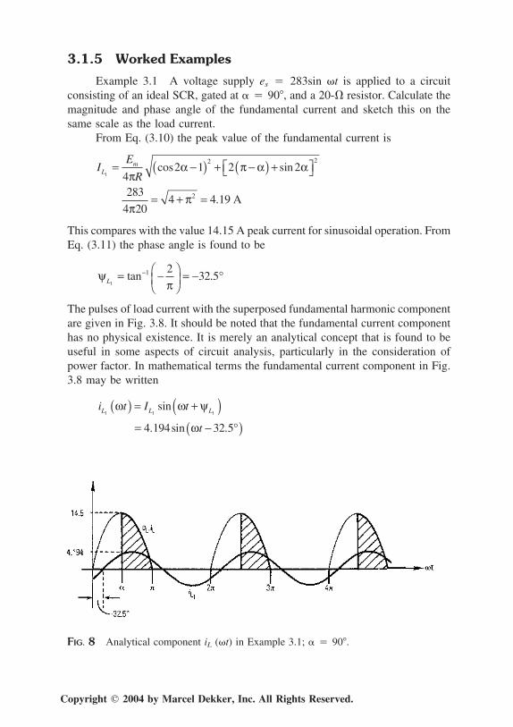
Example 3.1 A voltage supply es 283sin t is applied to a circuitconsisting of an ideal SCR, gated at 90, and a 20- resistor. Calculate themagnitude and phase angle of the fundamental current and sketch this on thesame scale as the load current.
From Eq. (3.10) the peak value of the fundamental current is
IE
RLm
1 42 1 2 2
283
4 204 4 19
2 2
2
= −( ) + −( ) +
= + =
πα π α α
ππ
cos sin
. A
This compares with the value 14.15 A peak current for sinusoidal operation. FromEq. (3.11) the phase angle is found to be
ψπL1
1 232 5= −
= − °−tan .
The pulses of load current with the superposed fundamental harmonic componentare given in Fig. 3.8. It should be noted that the fundamental current componenthas no physical existence. It is merely an analytical concept that is found to beuseful in some aspects of circuit analysis, particularly in the consideration ofpower factor. In mathematical terms the fundamental current component in Fig.3.8 may be written
i t I t
t
L L L1 1 1
4 194 32 5
ω ω ψ
ω
( ) = +( )= − °( )
sin
. sin .
FIG. 8 Analytical component iL (t) in Example 3.1; 90.
Copyright 2004 by Marcel Dekker, Inc. All Rights Reserved.

Single-Phase Controlled Rectifier Circuits 65
Example 3.2 A single-phase, half-wave controlled rectifier circuit has aresistive load R and an ideal sinusoidal supply es Em sin t. A capacitor C ofadjustable value is connected across the supply terminals. With a fixed value ofthyristor firing angle what is the value of C that will result in maximum powerfactor operation? If 90, Em 283 V, and R 10 , what value of Cwill give maximum power factor at f 50 Hz? What degree of power factorimprovement is realisable by the use of capacitance compensation?
The optimum value of C is given in Eq. (3.28). At 50 Hz, R 10 , /2,
C =×
=2
2000 250 65
π πµ. F
With this value of capacitance, C 0.0159 mho and Xc 62.9 . Minimumsupply current lsmin, from Eq. (3.29), is found to be
Ismin.= − +
=283
20
200
3956
1
26 36 A
In the absence of the capacitor the rms load current is obtained from Eq. (3.4)or from Eq. (3.29), with 1/Xc 0:
IL = =283
201 2 7 075/ . A
The average load power is therefore
P I RL L= = ( ) × =2 27 075 10 500. W
The uncompensated power factor is
PFP
E ILL
s L
= = ( ) ×=500
283 2 7 0750 353
/ .. lagging
In the presence of optimal capacitance the power factor becomes
PFP
E IL
s smax
min
.= = 0 393 lagging
The power factor has therefore been improved by 0.393/0.353, or about 11%,due to the optimal capacitance compensation.
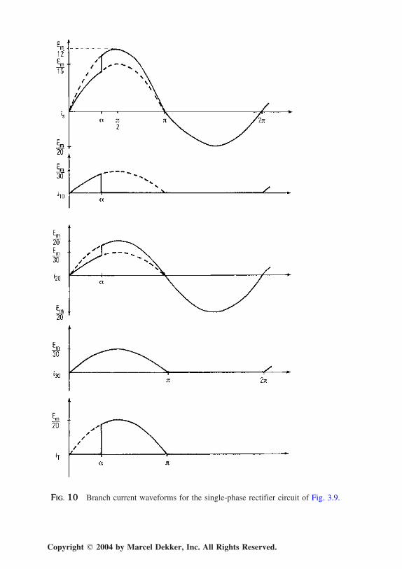
Example 3.3 A rectifier circuit containing two ideal diodes D and an idealsemiconductor switch (shown as an SCR) is given in Fig. 3.9. Sketch, on squaredpaper, a consistent set of waveforms for the supply voltage, the three resistor cur-
Copyright 2004 by Marcel Dekker, Inc. All Rights Reserved.
Chapter 366
FIG. 9 Single-phase rectifier circuit of Example 3.3.
rents, the switch current iT, and the supply current is if the SCR firing angle 60. Write a mathematical expression is (t) to define the waveform of the supplycurrent and calculate its average value over a supply cycle in terms of Em.
The waveforms of the various branch currents are shown in Fig. 3.10.
i tE
tE
tE
tsm m mω ω
αω
πα
ωππ
( ) = + +15 0 12 15
2sin sin sin
IT
i t d t
E td t
td t
td t
s s
T
m
av= ( )
= + +
∫1
2 15 12 20
0
2
ω ω
πω ω ω ω ω ω
π
sin sin sinππ
α
πα
∫∫∫
0
= −( ) + −( ) + −( )
=
Et t t
E
m
2
1
15
1
12
1
200
2
πω ω ω
α
α
π
π
πcos cos cos
mm
2
1
151
1
121
1
201 1
πα α−( ) + +( ) + − −( )
cos cos
IE E
Esm m
mav= + + −( )
( ) =2
1
15
1
2
1
12
3
2
1
202
20 0583 0 0093
π π. .
Example 3.4 A purely resistive load is supplied with power from an idealsingle-phase supply of fixed voltage and frequency, denoted by e Em sin t,through an arrangement of four ideal diodes and an ideal SCR switch (Fig. 3.11a).The switch is gated during every half cycle of its positive anode voltage state.Sketch (1) the supply current waveform and (2) the load current waveform fora switching angle of 60. Derive an expression for the rms value of the loadcurrent in terms of Em and . What is the per-unit value of this (compared with 0) when is 60?
Copyright 2004 by Marcel Dekker, Inc. All Rights Reserved.
Single-Phase Controlled Rectifier Circuits 67
FIG. 10 Branch current waveforms for the single-phase rectifier circuit of Fig. 3.9.
Copyright 2004 by Marcel Dekker, Inc. All Rights Reserved.

Chapter 368
FIG. 11 Single-phase, full-wave controlled rectifier of Example 3.4; 50.
The waveforms are shown in Fig. 3.11(b). Assuming ideal rectifiers
iE
Rt
E
RtL
m m= + − °( )+
sin sinωπα
ωπ
π α180
2
Now sin(t 180) sin t. Therefore,
i d tE
Rt tL
m= = +
∫ ∫ ∫ +
1
2 22
0
22
22 22
1 2
πω
πω ω
π
α
π
π α
πsin sin
/
IL But
sincos sin2 1 2
2 2
2
4∫ ∫= − = −ω ω ω ω ωt
td t
t t
Therefore,
IE
R
t t E
R
t tL
m m22
2
2
22 2
2
4 2 2
2
4
2= −
+ −
π
ω ω πα π
ω ω ππ
sin sin
++
= − +
+ − − ++( )
α
ππ α α π π α π αE
Rm2
22 2
2
4
2
2
2
4
sin sin
= − + + − +
E
Rm2
22 2
2
4 2
2
4ππ α α π α αsin sin
Copyright 2004 by Marcel Dekker, Inc. All Rights Reserved.

Single-Phase Controlled Rectifier Circuits 69
Therefore,
IE
RL
m= −( ) + 2
1
22 2
ππ α αsin
When 0,
IE
RL
m
0 2°=
When 60,
IE
R
E
R
E
R
Lm
m m
= +( )
= =
2
1
24 188 0 866
2
5 054
2 20 804
π
π
. .
..
Therefore,
IE
RL
m
60 20 897
°= ( ).
and
and IL L LpuI I= =
° °60 00 897/ .
3.2 SINGLE-PHASE CONTROLLED RECTIFIERCIRCUITS WITH SERIES R-L LOAD
3.2.1 Half-Wave Controlled Rectifier Circuit
An ideal sinusoidal supply voltage e Em sin t is applied to a series R-L circuit,Fig. 3.12, in which the current level is adjusted by the controlled switching of(for example) a thyristor. For switching angle and phase angle the instanta-neous current iL (t) is given by
i tE
ZtL
m tω ω α ε α ω( ) = −( ) − −( )
+ −( )sin sin cotΦ Φ Φ
(3.46)
When 0, Eq. (3.46) reduces to the expression Eq. (2.72) previously deducedfor diode operation.
Copyright 2004 by Marcel Dekker, Inc. All Rights Reserved.

Chapter 370
FIG. 12 Single-phase, half-wave controlled rectifier with series R-L load.
The extinction angle x of the load current is defined by a transcendentalequation [Eq. (3.47)], obtained by putting iL (x) 0 in Eq. (3.46)
sin(x ) sin( )εcot ( x) (3.47)
The conduction angle c per cycle is given by
c x (3.48)
If x is eliminated between Eqs. (3.47) and (3.48), it is seen that
sin(c ) sin( )εc cot (3.49)
Waveforms of the load voltage and current are given in Fig. 3.13 for a case when , and it may be seen that the nonsinudoidal, unidirectional current pulseslie within the envelope of the steady-state sinusoidal component of current. Afirst approximation value of c may be obtained from the simple relation
c (3.50)
where is of the order a few degrees for loads with 70.For 0 the current pulses lie outside the sinusoidal current envelope
in a similar manner to that illustrated in Fig. 2.10. In this latter case the conductionangle is given by the simple, approximate relation
θ π ααc < = + − + ∆Φ Φ (3.51)
Note that Eq. (3.51) is not the same as Eq. (3.50).When , the rectified current pulses become half sinusoids displaced
from the supply voltage by angle . Calculated characteristics of the conductionangle versus switching angle for a full range of load phase angles are given inFig. 3.14. The isosceles triangle at the top left-hand corner, bounded by the line and the 90 line, represents conditions when and conductionangles greater than radians are realized. The scalene triangle, bounded by the 0, 90, and lines represents the mode when and
Copyright 2004 by Marcel Dekker, Inc. All Rights Reserved.

Single-Phase Controlled Rectifier Circuits 71
FIG. 13 Waveforms for single-phase, half-wave controlled rectifier with series R-L load; 90.
conduction angles smaller than radians are realized. For both modes of operationthe average value Iav of the rectified load current is defined in the standard manner
I i t d t
E
Z
av L
mc c
c= ( )
= −( ) −( ) + −( )
+
∫1
2
21
πω ω
πθ α θ
α
θ α
cos cos sin tanΦ Φ ssin
sin tan cot
α
α ε θ
−( )
+ −( ) −
Φ
Φ Φ Φ c (3.52)
Copyright 2004 by Marcel Dekker, Inc. All Rights Reserved.

Chapter 372
FIG. 14 Conduction angle c thyristor switching-angle for the single-phase, half-wavecontrolled rectifier circuit.
An alternative form for Iav may be obtained by eliminating the exponential compo-nent between Eqs. (3.52) and (3.49), but this does not appear to render anycomputational advantage.
The rms value IL of the supply current is defined by
I i t d tL L
c2 21
2= ( )+
∫πω ω
α
θ α
(3.53)
The substitution of Eq. (3.46) into Eq. (3.53) yields an expression containingexponential terms which cannot be eliminated by the use of the relationships Eq.(3.47) or (3.49)
IE
ZL
mc c c c
22
22 2
42 2= − − +( ) − −( )
+
−
πθ θ α θ θ ε αsin cos sin tan
si
cotΦ Φ Φ Φ
nn tan
sin sin sin sin sincot
2
4 4
α
θ θ α ε αα
−( )
+ −( ) +( ) −−
Φ Φ
Φ Φ ΦΦc c ssin α −( )Φ (3.54)
Copyright 2004 by Marcel Dekker, Inc. All Rights Reserved.

Single-Phase Controlled Rectifier Circuits 73
When 0, Eq. (3.54) reduces to Eq. (2.63).Conduction angle c can be extended, and thus the average and rms load
currents increased by the use of a freewheel diode FWD across the load (Fig.3.15). If the load is sufficiently inductive the load current will become continuous.Instant commutation (i.e., switch-off) of the thyristor T will then occur at theinstants where the supply voltage goes negative.
In general the load current can be thought to consist of two modal elementsdue to two modes of circuit operation. While the freewheel diode conducts, theload voltage is zero and the current decays exponentially with a time constant L/R. Therefore, for t 2 , in Fig. 3.16,
i tL
tω ε ω ω( ) =− −R
Lcot Φ−−( )
iL ( )____
ε= iL ( ) tω −−( )(3.55)
While the switch conducts in Fig. 3.15, the diode blocks and the operation issimilar to that of Fig. 3.12. Therefore, for t , in Fig. 3.16, the currentis defined by the expression Eq. (3.46) plus a transient that has a value iL () att and decays exponentially thereafter.
i tE
Zt
i
Lm t
Lt
ω ω α ε
α ε
ω α
ω
( ) = −( ) − −( )
+ ( )
− −( )
−
sin sin cot
cot
Φ Φ Φ
Φ −−( )α (3.56)
When t , the two modal current equations, Eqs. (3.55) and (3.56), are equal.Equation (3.56) then becomes
iE
ZiL
mLπ π ε α απ α( ) = −( ) − − −( ) − −( )sin sincotΦ ΦΦ
(3.57)
FIG. 15 Single-phase, full-wave controlled rectifier circuit with freewheel diode.
Copyright 2004 by Marcel Dekker, Inc. All Rights Reserved.

Chapter 374
FIG. 16 Steady-state load current and voltage waveforms for the freewheel diode circuitof Fig. 3.15; 50.
For cyclic operation iL () iL (2 ), so that in Eq. (3.55),
iL (2 ) iL () iL ()εcot () (3.58)
Equations (3.57) and (3.58) are simultaneous and can be solved to give valuesfor iL () and iL (). For a complete supply voltage cycle t 2 ,the load current is given by adding, Eqs. (3.55) and (3.56):
i tE
Zt
i Z
ELm L
m
ω ω αα
ε( ) = −( ) − −( ) −( )
sin sinΦ Φ
+ ( ) +− −( )
α
π
ππ επ α
πiL
cot Φ 2ωt
− −( )αcot Φ ωt
(3.59)
The average and rms values of iL (t) can be obtained from the respective definingintegrals in Eqs. (3.52) and (3.53).
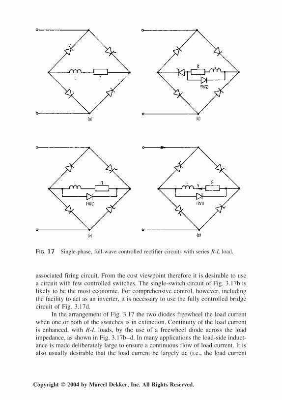
3.2.2 Single-Phase, Full-Wave Controlled CircuitsEach of the circuit configurations of Fig. 3.4 can be used for full-wave rectificationof a series R-L load, as in Fig. 3.17. The cost of a diode switch is much less thanthat of a controlled switch of the same rating, and it also does not require an
Copyright 2004 by Marcel Dekker, Inc. All Rights Reserved.
Single-Phase Controlled Rectifier Circuits 75
FIG. 17 Single-phase, full-wave controlled rectifier circuits with series R-L load.
associated firing circuit. From the cost viewpoint therefore it is desirable to usea circuit with few controlled switches. The single-switch circuit of Fig. 3.17b islikely to be the most economic. For comprehensive control, however, includingthe facility to act as an inverter, it is necessary to use the fully controlled bridgecircuit of Fig. 3.17d.
In the arrangement of Fig. 3.17 the two diodes freewheel the load currentwhen one or both of the switches is in extinction. Continuity of the load currentis enhanced, with R-L loads, by the use of a freewheel diode across the loadimpedance, as shown in Fig. 3.17b–d. In many applications the load-side induct-ance is made deliberately large to ensure a continuous flow of load current. It isalso usually desirable that the load current be largely dc (i.e., the load current
Copyright 2004 by Marcel Dekker, Inc. All Rights Reserved.

Chapter 376
should have the largest realizable average value) with low ripple content. Theideal load current ripple factor, Eq. (2.11) is zero, which occurs when the loadcurrent is pure dc.
The four-switch circuit of Fig. 3.17d has the load voltage and current wave-forms shown in Fig. 3.18 for 30, with large L. Commutation of the twoconducting switches occurs naturally at the end of a supply voltage half cycle.The load voltage is seen to be the full-wave equivalent of the corresponding half-wave voltage waveform of Fig. 3.16. From Fig. 3.18 it is seen that the averageload voltage is given by
E E t d tE
av mm= = +( )∫
11
πω ω
πα
α
πsin cos (3.60)
FIG. 18 Voltage and current waveforms for the single-phase, full-wave circuit of Fig.3.17d, large L, 30.
Copyright 2004 by Marcel Dekker, Inc. All Rights Reserved.

Single-Phase Controlled Rectifier Circuits 77
Also,
Iav Id (3.61)
The output power is dissipated in resistor R. With ideal switches and a losslessinductor L the output power also equals the input power
Pout Pin I2dR (3.62)
The input current is defined by the expression
i t I Is d dωπα
ππ α
( ) = −+
2(3.63)
The rms value of the input current is given by
I i t d t
I d t
I
s s
d
d
= ( )
=
= −
∫
∫
1
2
1
2
0
2
2
πω ω
πω
π απ
π
α
π
(3.64)
When 0, Is Id. The fundamental component of the supply current is foundto have the rms magnitude
I Is d1
2 2
2=
πα
cos (3.65)
By inspection of the supply current waveform in Fig. 3.18, it is seen that thedisplacement angle is 1 is /2. The input power may therefore be alternativelydefined as
P EI
E I
s
d
=
=
1 1
22 2
2
cos
cos
ψ
πα
(3.66)
Note that real or average power P is associated only with the combinations ofvoltage and current components of the same frequency. Since the supply voltageis sinusoidal and therefore of single frequency, it combines only with the funda-mental (supply frequency) component of the input current. The combination ofthe fundamental voltage component with higher harmonic components of thecurrent produces time-variable voltamperes but zero average power.
Copyright 2004 by Marcel Dekker, Inc. All Rights Reserved.

Chapter 378
The power factor of the bridge circuit is obtained using Eqs. (3.64) and(3.66)
PFP
EI
E I
EI
s
d
d
=
=−
=−
2 22
22 2
2
2
πα
π α
πα
π α
cos /
cos /
π
(3.67)
When 0, it is seen that PF 22 / 0.9. The displacement factor anddistortion factor components of the power factor can be obtained via the Fouriercomponents a1b1 of is, (t), Sec. 3.13.
When a freewheel diode is not used the symmetrical triggering of oppositepairs of switches in Fig. 3.17d (or Fig. 3.4d) results in the waveforms of Fig.3.19, for a highly inductive load. Compared with Fig. 3.16 the load current isunchanged and so therefore is the power dissipation. But note that the rms valueof the supply current is increased so that the power factor is reduced. It is seenfrom Fig. 3.19 that the average load voltage is given by
E E t d tE
av mm= =
+
∫1 2
πω ω
πα
π αsin cos α (3.68)
Also, the average voltage of the load inductor is zero so that
I IE
Rav dav= = (3.69)
The rms value EL of the load voltage in Fig. 3.19 is given by
E E t d tL m2 2 21=
+
∫πω ω
α
π αsin
Or
EE
Lm=2 (3.70)
The harmonic nature of the load current in Fig. 3.17 could be obtained by calculat-ing the Fourier series for the periodic function iL (t), for an arbitrary R-L load,
Copyright 2004 by Marcel Dekker, Inc. All Rights Reserved.
Single-Phase Controlled Rectifier Circuits 79
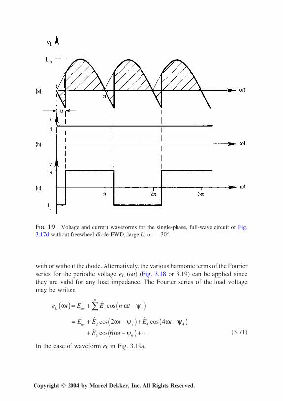
FIG. 19 Voltage and current waveforms for the single-phase, full-wave circuit of Fig.3.17d without freewheel diode FWD, large L, 30.
with or without the diode. Alternatively, the various harmonic terms of the Fourierseries for the periodic voltage eL (t) (Fig. 3.18 or 3.19) can be applied sincethey are valid for any load impedance. The Fourier series of the load voltagemay be written
e t E E n t
E E t E t
L av n
n
n
av
ω ω ψ
ω ψ ω
( ) = + −( )
= + −( ) + −
∑ ˆ cos
ˆ cos ˆ cos
1
2 2 42 4 ψψ
ω ψ4
6 66
( )+ −( ) +ˆ cosE t … (3.71)
In the case of waveform eL in Fig. 3.19a,
Copyright 2004 by Marcel Dekker, Inc. All Rights Reserved.
Chapter 380
ˆ cos
ˆ cos
EE
EE
m
m
2
4
21
1
9
2
32
2
1
9
1
25
2
152
= + −
= + −
πα
πα
ˆ cos
ˆ( ) ( )
cos
EE
EE
n n n
m
nm
6
2 2 2
2
1
25
1
49
2
352
2
1
1
1
1
2 2
= + −
=+
+−
−−
πα
πα
11
. . .
(3.72)
and
ψα αα α
ψα
21
41
3 3
3 3
3 3 5
=− ( )− ( )
=( ) −
−
−
tansin sin /
cos cos /
tansin / sin αα
α α( )
( ) − ( )/
cos / cos /
5
3 3 5 5
…
ψα ααn
n n n n
n n=
−[ ] −( ) − +[ ] +( )−[ ] −
−tansin( ) / sin( ) /
cos( ) /1 1 1 1 1
1 1(( ) − +[ ] +( )cos( ) /n n1 1α (3.73)
When the harmonic voltage terms of Eq. (3.71) are applied to the series R-L loadof Fig. 3.17, the following series is obtained for the load current
i t I I n t
I I t I
L av n L L
n
av
( ) cos( )
cos( ) c
ω ω ψ
ω ψ
= + − −
= + − − +
∑ Φ
Φ1
2 2 2 42 oos( )
cos( )
4
6
4 4
6 6 6
ω ψ
ω ψ
t
I t
− −
+ − − +
Φ
Φ …
ˆ
ˆ
ˆ
ˆ
(3.74)
where Iav is given by Eq. (3.69)and
ˆˆ
( )
ˆˆ
( )
IE
R L
IE
R L
2
2
2 2
4
4
2 2
2
4
=+
=+
ω
ω
Copyright 2004 by Marcel Dekker, Inc. All Rights Reserved.
Single-Phase Controlled Rectifier Circuits 81
…
ˆˆ
( )I
E
R n Ln
n=+2 2ω (3.75)
Also,
Φ
Φ
21
41
2
4
=
=
−
−
tan
tan
ω
ω
L
RL
R
…
Φn
n L
R= −tan 1 ω
(3.76)
A close approximation to the rms current IL for any R-L load can be obtained byusing the square law relationship of Eq. (2.12). If the load impedance is highly in-ductive, the harmonic terms in Eqs. (3.71)–(3.76) are negligibly small. The loadcurrent is then constant at the value IL or Id, which also becomes its rms value IL.
A further application of this bridge circuit in the form of a dual converteris described in Sec. 12.2.1.
3.2.3 Worked ExamplesExample 3.5 A series semiconductor switching circuit, Fig. 3.12, has a
load in which the resistance is negligibly small. Deduce and sketch the waveformsof the load voltage and current for a firing angle smaller than the load phaseangle . What are the average values of the load current and voltage?
When 90, cot 0 and Eq. (3.46) reduces to
i tE
ZtL
m( ) ( cos cos )ω ω α= − +(3.77)
The variation of iL (t) is shown in Fig. 3.20 for the case when 60. It isseen that the current waveform is symmetrical about so that extinction anglex is given by
x 2
From Eq. (3.48), therefore,
c 2( ) (3.78)
Equation (3.52) is indeterminate for 90, but a solution for the time averagecurrent can be obtained by integrating Eq. (3.77)
Copyright 2004 by Marcel Dekker, Inc. All Rights Reserved.

Chapter 382
FIG. 20 Voltage and current waveforms for the single-phase, full-wave controlled recti-fier circuit with highly inductive load; 30.
iE
Zt d t
E
Z
E
Zt
avm
m m
c= −
= −
+
−
∫
∫
1
2
2
2
πα ω ω
πα ω
α
α θ
α
π α
(cos cos )
(cos cos ) dd t
E
Zm
ω
ππ α α α= − +[ ]( ) cos sin
Copyright 2004 by Marcel Dekker, Inc. All Rights Reserved.

Single-Phase Controlled Rectifier Circuits 83
When 0, Iav Em/L. The output average current is then constant at itsmaximum realizable value, which represents ideal rectifier operation. The voltageacross the load inductor may be obtained by differentiating the current expressionEq. (3.77), noting that |Z| L:
e t Ldi
dtL
di
d t
E t t
LL L
m
( )( )
sin
ω ωω
ω α ω π α
= =
= < < − for 2
The average value Eav of eL (t) may be obtained by the usual integration methodand is found to be zero, as can be seen by inspection in Fig. 3.20.
Example 3.6 In the series R-L circuit of Fig. 3.12R 25 , L 150mH. The supply voltage is given by e Em sin t, where Em 400, V at afrequency of 50 Hz. Calculate the average load current for the SCR firing angles(1) 30 and (2) 120.
At 50 Hz,
ω π
ω
L
L
R
= = Ω
= = =− −
100150
100047 12
47 12
25621 1
.
tan tan. oΦ
Z R L= + = Ω
= == =
2 2 2 53 34
62 0 532
62 1 88
ω .
cot cot .
tan tan .
o
o
ΦΦ
sin( ) sin(30 62) 0.53
sin( ) sin(120 62) 0.85
cos( ) cos(32) 0.85
or
cos( ) cos(58) 0.53
1. 30: In this case and an estimation of the conduction angle canbe made from Eq. (3.51)
θ π αc = + − + = + − + =Φ ∆ 180 62 30 7 219o o o o o (say)
The value c 219 is used as a first guess in Eq. (3.49). By iteration it is foundthat c 216.5. The accuracy with which c can be read from Fig. 3.18 issufficient for most purposes.
cosc 0.804
Copyright 2004 by Marcel Dekker, Inc. All Rights Reserved.
Chapter 384
sinc 0.595
Iav =×
− − − −[ +400
2 53 341 804 0 85 0 595 1 88 0 53 0 85 1 88
π .. ( . ) ( . . )( . ) . ( . ))( . )
. .
0 134
1 194 3 059
]= ×
.3 65= A
2. 150: In this case and the use of Eq. (3.50) gives
θ π αc = + − −
= + − − =
Φ ∆
180 62 150 15 77o o o o o (say)
The characteristics of Fig. 3.14 suggest that this figure is high and should beabout 60. Iteration from Eq. (3.49) gives a value c 64. In Eq. (3.52),
cosc 0.44
sinc 0.9
Iav =×
+ −[ +400
2 53 340 56 0 53 0 9 1 88 0 85 0 85 1 88 0 5
π .. ( . ) ( . . )( . ) . ( . )( . 552
1 194 0 346 0 413
)
. . .
]= × = A
Example 3.7 A half-wave, controlled rectifier circuit has a series R-L loadin which tan1 (L/R) 80. The ideal single-phase supply voltage isgiven by e Em sin t. Explain the action for a typical steady-state cycle when 60 and the circuit includes a freewheel diode (Fig. 3.15). What effect doesthe diode have on circuit power factor?
The load voltage and current are shown in Fig. 3.16. The supply current is(t) is given by the portions of the current curve between → , 2 →3, etc., noting that is () is (2 ) 0. The nonzero value of the loadcurrent at t is due to residual current decaying through the diode duringthe extinction of the thyristor switch. In the presence of the diode, the energystored in the magnetic field of the inductor is dissipated in resistor R rather thanbeing returned to the supply. Current and power flow from the supply to theload only occur during the conduction intervals of the thyristor. Because of thesignificantly increased rms load current (compare the load currents in Figs. 3.14and 3.16) however, the load power dissipation is significantly increased. All ofthis power must come from the supply, although not at the instants of time inwhich it is dissipated. The supply voltage remains sinusoidal at all times.
The power factor, seen from the supply point, is
PFP
EI=
Copyright 2004 by Marcel Dekker, Inc. All Rights Reserved.

Single-Phase Controlled Rectifier Circuits 85
The rms supply voltage E Em/2 is constant. The rms supply current I probablyincreases by (say) 20%. But the power dissipation can be assessed in terms ofthe rms value of the load current. Comparing iL (t) in Figs. 3.13 and 3.16suggests that rms value IL is at least doubled and the power increases at leastfour times. The presence of the freewheel diode therefore causes the power factorto increase.
Example 3.8 A single-phase, full-wave bridge circuit, Fig. 3.21, has fourideal thyristor switches and a highly inductive load. The electrical supply is idealand is represented by e Em sin t. Sketch waveforms of the load current,supply current and load voltage for 60 Calculate the rms value of the supplycurrent and the power factor of operation, in terms of .
The waveforms of operation with a highly inductive load are given in Fig.3.19. The supply current is represented by the relation
i t I Is d d( ),
,ω
α
π α
π α
α π= −
+
+0
2
This has an rms value defined by
I i t d ts s= ∫1
22
0
2
πω ω
π( )
Therefore,
I I d t I d ts d d2 2 2
0
1
2= + −
+
+
∫∫πω ω
π α
α
α
π α( )
,
FIG. 21 Single-phase, full-wave controlled rectifier circuit with highly inductive load.
Copyright 2004 by Marcel Dekker, Inc. All Rights Reserved.

Chapter 386
The rms value of the negative parts of the wave is equal to the rms value of thepositive parts so that
I I d t Is d d2 2 21 1= = + −
+
∫πω
ππ α α
α
π α( )
Therefore,
Is Id
As varies, the waveform of is (t) is unchanged and so is its rms value, butthe switchover from positive to negative value occurs at the firing points.
Power dissipation is determined by the rms value of the load current
P I R I RL d= =2 2
The power factor is found to be
PFP
EI
I R
EI
I R
Ed
d
d= = =2
where E Em 2 .But from Eq. (3.68),
IE
R
E
Rdav m= =
2
παcos
The power factor is therefore
PF = 2 2
παcos
When 0, the PF 22 /, which agrees with the value for a full-wavediode bridge.
Example 3.9 In the single-phase, full-wave rectifier of Fig. 3.21 the loadconsists of R 10 and L 50 mH. The ideal sinusoidal supply voltage isdefined as es 2402 sin t at 50 Hz. Calculate values for the average and rmsload currents, the power dissipation and the power factor at the supply terminals ifthe thyristor firing angle 45.
The circuit of Fig. 3.21 is seen to be a topological rearrangement of Fig.3.17d, without the freewheel diode. The load voltage has the segmented sinusoidalform of Fig. 3.19a for any R-L load if the load current is continuous. The loadcurrent will be of some waveform intermediate between that of Fig. 3.19b (whichis only valid for highly inductive loads) and the corresponding segmented sinusoi-dal waveform (not given) obtained with purely resistive loads.
Copyright 2004 by Marcel Dekker, Inc. All Rights Reserved.

Single-Phase Controlled Rectifier Circuits 87
At supply frequency the phase-angle of the load impedance is given by
=
= × ××
= =
−
− −
tan
tan tan . .
1
1 1100 50
1000 101 57 57 5
ω
π
L
R
Since , the mode of operation is that of continuous load current and theequations of the present Sec. 3.2.2 are valid.
The average load current is given by Eqs. (3.68) and (3.69):
IE
RAav
m= = ××
× =2 2 240 2
1057 5 11 61
πα
πcos cos . .
In order to calculate the rms load current, it is necessary to calculate its Fourierharmonics. From Eq. (3.72), cos 2 cos 90 0, and the peak values of thelower order load voltage harmonics are
E2 56.92 V E4 20.99 V E6 13.27 V
Also, in Eq. (3.62) the following impedances are offered by the load at the speci-fied harmonic frequencies.
Z R L
Z R L
Z R L
22 2
42 2
62 2
2 32 97
4 63 62
6 94 78
= + ( ) =
= + ( ) =
= + ( ) =
ω
ω
ω
.
.
.
The peak values of the current harmonics are therefore
ˆ .
..I A2
56 92
32 971 726= =
ˆ .
..I A4
20 99
63 620 33= =
ˆ .
..I A6
13 27
94 780 14= =
From Eq. (2.12) the rms value of the load current is given by
I I I I IL av2 2
22
42
621
2= + + + +( )ˆ ˆ ˆ …
and
Copyright 2004 by Marcel Dekker, Inc. All Rights Reserved.

Chapter 388
IL = ( ) + ( ) + ( ) + ( )
= + =
11 611
21 726 0 33 0 14
134 79 1 554 11
2 2 2 2. . . .
. . ..68 A
It is seen that the effects of the fourth and sixth harmonic current componentson the total rms value are negligible. The load power is seen, from Eq. (3.64),to be
P WL = ( ) × =11 68 10 1364 222
. .
and this is also the power entering the circuit terminals, neglecting rectifier ele-ment losses. The rms value of the supply current is equal to the rms value of theload current. The power factor at the supply point is, therefore,
PFP
E IsL
s s
= =×
=1364 22
240 11 680 487
.
..
This compares with the value cos cos 57.5 0.537 for the load impedancealone.
PROBLEMS
Single-Phase Controlled Rectifier Circuits: R Load
3.1 A single controlled rectifier controls the current to a resistive load in asingle-phase sinusoidal circuit (Fig. 3.1). Derive expressions for the aver-age value and rms value of the load current at an arbitrary firing angle if e Em sin t. What is the lowest value of ripple factor for this system?Sketch the variations of Iav and Irms versus firing angle.
3.2 Sketch the currents for the circuit of Fig. 3.22 if e Em sin t; R1 R2
and 60. What is the average value of the supply current if Em 100 V and R1 R2 10 ?
3.3 In the circuit of Fig. 3.22; R1 R2 10 and the supply voltage is e Em sin t. Sketch, roughly in proportion, corresponding waveforms ofthe supply voltage and the three branch currents for a typical supply voltagecycle if 90. Calculate the power dissipation in the circuit for firingangles of 0 and 180 and thereby estimate the dissipation when 90.What harmonic frequency components would you expect to find in thesupply current?
3.4 The circuit of Fig. 3.23 consists of identical resistors R1 R2 10 ,an ideal diode D, and an ideal SCR designated T supplied from an ideal
Copyright 2004 by Marcel Dekker, Inc. All Rights Reserved.
Single-Phase Controlled Rectifier Circuits 89
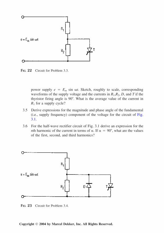
FIG. 22 Circuit for Problem 3.3.
power supply e Em sin t. Sketch, roughly to scale, correspondingwaveforms of the supply voltage and the currents in R1,R2, D, and T if thethyristor firing angle is 90. What is the average value of the current inR1 for a supply cycle?
3.5 Derive expressions for the magnitude and phase angle of the fundamental(i.e., supply frequency) component of the voltage for the circuit of Fig.3.1.
3.6 For the half-wave rectifier circuit of Fig. 3.1 derive an expression for thenth harmonic of the current in terms of . If 90, what are the valuesof the first, second, and third harmonics?
FIG. 23 Circuit for Problem 3.4.
Copyright 2004 by Marcel Dekker, Inc. All Rights Reserved.

Chapter 390
3.7 Derive an expression for the average power dissipation in the half-waveresistor circuit of Fig. 3.1. At 90, what proportion of the total powerdissipation is associated with the fundamental component of current?
3.8 An ideal voltage source e Em sin t supplies power to a single-phase,half-wave controlled rectifier circuit with resistive load (Fig. 3.1). Obtainan expression for the circuit power factor in terms of Em and thyristorswitch firing angle .
3.9 What is the effect on the supply current of connecting a capacitor acrossthe supply terminals of a thyristor controlled resistive circuit (Fig. 3.3)?If Xc R, is there a value of firing angle that results in unity powerfactor operation?
3.10 A l00 resistor is supplied with power from an ideal voltage source e 330 sin 314t via a thyristor. At what value of firing angle is the powerdissipation one-third of the value for sinusoidal operation?
3.11 Show that the power factor of the single-phase, half-wave rectifier circuitof Fig. 3.1 is given by
PF =−( ) +2 2
2
π α απ
sin1
2
3.12 For the half-wave rectifier with resistive load (Fig. 3.1), show that thephase-angle of the fundamental component of the current, with respect tothe supply voltage, is given by
ψ απ α α1
1 2 1
2 2= −
− +−tan
cos
( ) sin
Sketch the variation of 1 with firing angle for 0 .3.13 The single-phase half-wave rectifier circuit of Fig. 3.1 is compensated by
a terminal capacitance as in Fig. 3.3, where Xc R. Sketch waveformsof the load current, capacitor current, and supply current for 90. Isit possible to assess the effect on the overall power factor from a considera-tion of the three waveforms?
3.14 Derive expressions for the current distortion factor and current displace-ment factor of the half-wave rectifier circuit of Fig. 3.1. Sketch the varia-tions of these for 0 . If a power factor correction capacitor isused with Xc R, derive new expressions for the distortion factor anddisplacement factor of the input current. How has the connection of thecapacitor affected (a) the distortion factor and (b) the displacement factor?
Copyright 2004 by Marcel Dekker, Inc. All Rights Reserved.

Single-Phase Controlled Rectifier Circuits 91
FIG. 24 Circuit for Problem 3.15.
3.15 A thyristor switch T controls the load current in the resistor circuit of Fig.3.24. What is the effect on the load current of connecting diode D in thecircuit?
3.16 A resistive load is supplied through a thyristor connected in the secondarycircuit of a single-phase transformer with low leakage reactance (Fig. 3.25).Sketch the forms of the load current, supply current, and thyristor voltageover a supply voltage period.
3.17 A full-wave controlled rectifier (Fig. 3.11a) operates from a sinusoidalsupply e Em sin t. Derive an expression for the ripple factor (RF) ofthe load voltage with resistive load. Calculate values of this at the firingangles 0, 30, 60, 90, 120, and 180, and sketch the variation of RFversus .
3.18 Show that the power factor of a single-phase, full-wave controlled bridgerectifier circuit with resistive load is given by
FIG. 25 Circuit for Problem 3.16.
Copyright 2004 by Marcel Dekker, Inc. All Rights Reserved.

Chapter 392
PF = −( ) + 1
22 2
ππ α αsin
Sketch the variation of PF with firing-angle over the range 0 .3.19 Show that the distortion factor and the displacement factor of the supply
current to the full-wave bridge circuits of Fig. 3.4 are given by Eqs. (3.44)and (3.35), respectively. What are the values of the distortion factor, dis-placement factor, and power factor at 90? What value of shuntconnected terminal capacitance would give the maximum realistic im-provement of power factor at 90 if Em 400 V, R 100 , andf 50 Hz?
3.20 The single-phase bridge rectifier circuit of Fig. 3.4b has the load currentwaveform of Fig. 3.5. Calculate the average and rms values of this wave-form and hence calculate the rms value of the ac ripple components.
3.21 In the circuit of Fig. 3.4(d) the current in load resistor R is controlledby the switching of two ideal thyristors. The ideal power supply has aninstantaneous voltage e Em sin t.
a. Sketch waveforms of the load current and supply current when eachthyristor is gated at 90 of its respective anode voltage.
b. If one thyristor fails by open circuit, sketch the resulting supply currentwaveform, and calculate its average value at 90 if R 10 and Em 100 V.
3.22 The single-phase bridge circuits of Fig. 3.4 are alternative configurationsfor achieving the same circuit performance. What are the advantages anddisadvantages of each circuit?
3.23 The single-phase, full-wave bridge circuit of Fig. 3.4(d) has a resistiveload. Opposite pairs of thyristors in the bridge arms are triggered symmetri-cally at a firing-angle 45. Sketch waveforms of the load current,supply current, and load voltage.
3.24 For the single-phase, full-wave bridge of Problem 3.23, obtain expressionsfor the average and rms values of the load current and hence the loadcurrent ripple factor. Calculate the power dissipation if e Em sin t,where Em 400 V, R 100 , and 45.
3.25 Calculate the Fourier coefficients a and b for the fundamental componentof the line current in Problem 3.23. Hence calculate the fundamental supplycurrent and the distortion factor in terms of Em, R and .
3.26 Obtain an expression for the power factor of the resistively loaded, full-wave, single-phase bridge of Problem 3.23. Sketch the variation of powerfactor with firing angle for 0 .
Copyright 2004 by Marcel Dekker, Inc. All Rights Reserved.

Single-Phase Controlled Rectifier Circuits 93
Single-Phase Controlled Rectifier Circuits: R-L Load
3.27 Deduce and sketch waveforms of the current, inductor voltage, and rectifiervoltage when a thyristor is gated at angle in the series R-L circuit ofFig. 3.12 if , where tan1 (L/R)
3.28 Derive expressions for the average and rms values of the rectified currentpulses in the circuit of Fig. 3.12 for an arbitrary value of firing angle ( ).
3.29 For the single-phase series R-L circuit (Fig. 3.12), show that if ,the current extinction occurs at an angle t x after the supply voltageis zero, where sin(x ) sin( )εcot (x ). Calculate thevalue of x if 30 and is (a) 60, (b) 90, and (c) 120.
3.30 Sketch the current waveform for a series R-L circuit controlled by a seriesthyristor. If the load phase angle to fundamental currents is 60, whatis the approximate extinction angle if 30? What difference is madeto the current waveforms by the connection of freewheel diode as in Fig.3.15?
3.31 In the circuit of Fig. 3.12, R 10 and L 50 mH. If es 2402sin t at 50 Hz, calculate (a) average and rms values of the current, (b)ripple factor, (c) power dissipation, (d) power factor for a thyristor firingangle 60.
3.32 In Problem 3.31 a flywheel diode is now connected across the load imped-ance, as in Fig. 3.15. Calculate the average value of the load current.
3.33 For the circuit of Fig. 3.15, sketch waveforms of the supply voltage, thyris-tor voltage, load voltage, and the three branch currents for 60, assum-ing continuous load current.
3.34 Repeat Problem 3.33 for a case when the combination of thyristor firingangle and load impedance phase angle are such that the load current isdiscontinuous.
3.35 In the circuit of Fig. 3.15, R 10 , L 50 mH and e Em sin t at50 Hz. If a capacitor is connected across the supply terminals, is this likelyto give any power factor correction?
3.36 A single-phase, full-wave bridge (Fig. 3.17d) has a highly inductive load.Sketch waveforms of the load voltage and current (a) with the freewheeldiode and (b) without the freewheel diode. In each case derive an expres-sion for the average load voltage in terms of R, , and Em if e Em sint.
Copyright 2004 by Marcel Dekker, Inc. All Rights Reserved.

Chapter 394
3.37 For the single-phase bridge circuit of Fig. 3.17d, with highly inductiveload, obtain an expression for the rms value of the supply current andhence show that the power factor is given by Eq. 3.67.
3.38 For the single-phase, full-wave bridge circuit of Fig. 3.17d with highlyinductive load, calculate the Fourier coefficients a1 and b1 of the fundamen-tal component of the supply current. Hence calculate the distortion factor,displacement factor, and power factor.
3.39 For the single-phase full-wave bridge circuit of Fig. 3.17d, a capacitor Cis connected across the terminals of the ideal supply. If the capacitor is ofsuch a value that Ic Id, sketch waveforms of the supply current is (t)with and without the capacitor. Do the waveforms indicate if any powerfactor correction is likely to be obtained?
3.40 A single-phase, full-wave bridge circuit (Fig. 3.17d) has the waveformsof Fig. 3.18 when the load is highly inductive. Obtain expressions for therms value Is1 and displacement angle 1 of the fundamental componentis1 (t) of the supply current. Sketch fundamental component is1 (t) ontothe waveform is (t) in Fig. 3.18c.
3.41 Use the values of Is1 and 1 from Problem 3.40 to obtain an expressionfor the reactive voltamperes Q entering the circuit where Q EIs1 sin 1.
3.42 The total apparent voltamperes S entering the circuit of Fig. 3.17 from thesinusoidal supply is given by
S2 E2I2s P2 Q2 D2
where P is the average power, Q is the reactive voltamperes, and D is thedistortion (or harmonic) voltamperes. Show that for a highly inductiveload the distortion voltamperes is given by
D E Id2 2 2
228
2= − −
π αα π
αcos
3.43 A single-phase bridge circuit (Fig. 3.21) is supplied from an ideal supplye Em sin t. If the load is highly inductive, deduce the waveform ofthe supply current and calculate the Fourier components a1 and b1, of itsfundamental component. Hence derive expressions for the distortion factor,displacement factor, and power factor.
3.44 Repeat Problem 3.40 for the circuit of Fig. 3.21.
3.45 Repeat Problem 3.41 for the circuit of Fig. 3.21.
3.46 Repeat Problem 3.42 for the circuit of Fig. 3.4d and hence show that
Copyright 2004 by Marcel Dekker, Inc. All Rights Reserved.

Single-Phase Controlled Rectifier Circuits 95
D E Id2 2 2
2
12 2= −
π
3.47 Calculate the Fourier coefficients a1 and b1 for the load voltage of Fig.3.19a. Hence show that the nth harmonic is given by Eq. (3.72) with thephase-angle given by Eq. (3.73).
3.48 In the single-phase, full-wave rectifier of Fig. 3.17d the load impedanceelements are R 20 and L 100 mH. The supply voltage is es 240 2 Em sin t at 50 Hz. If the firing angle 30, calculate (a)values of average and rms currents, (b) average power dissipation, and (c)power factor. Use the Fourier series method.
3.49 A single-phase, full-wave bridge rectifier circuit (Fig. 3.21) has a series R-L load of phase angle 60. If the thyristor switches are symmetricallytriggered at 30, sketch the load current and load voltage waveforms,assuming ideal sinusoidal supply.
3.50 For Problem 3.49, how do the average and rms values of the load currentwaveform compare with corresponding values obtained from the half-wavecircuit of Fig. 3.12?
Copyright 2004 by Marcel Dekker, Inc. All Rights Reserved.