single port 10/100 fast ethernet transceiver - recomb-omsk.ru · ip101a lf-ds-r02 ; add crystal...
TRANSCRIPT

IP101A LFData Sheet
1/38 Jul 24, 2008Copyright © 2004, IC Plus Corp. IP101A LF-DS-R15
Single port 10/100 Fast Ethernet Transceiver
Features
10/100Mbps TX Full-duplex or half-duplex Supports Auto MDI/MDIX function Fully compliant with IEEE 802.3/802.3u Supports IEEE 802.3u auto-negotiation Supports MII / RMII / SNI interface IEEE 802.3 full duplex control specification Supports Automatic Power Saving mode Supports BaseLine Wander (BLW)
compensation Supports Interrupt function Supports repeater mode Single 3.3V power supply with built-in 2.5V
regulator DSP-based PHY Transceiver technology Using either 25MHz crystal/oscillator or
50MHz oscillator REF_CLK as clock source Flexible LED display for speed, duplex, link,
activity and collision Supports flow control to communicate with
other MAC through MDC and MDIO 0.25u, CMOS technology 48-pin LQFP Support Lead Free package (Please refer to
the Order Information)
General Description
IP101A LF is an IEEE 802.3/802.3u compliant single-port Fast Ethernet Transceiver for both 100Mbps and 10Mbps operations. It supports Auto MDI/MDIX function to simplify the network installation and reduce the system maintenance cost. To improve the system performance, IP101A LF provides a hardware interrupt pin to indicate the link, speed and duplex status change. IP101A LF also provides Media Independent Interface (MII) / Serial Network Interface (SNI) or Reduced Media Independent Interface (RMII) to connect with different types of 10/100Mbps Media Access Controller (MAC). IP101A LF is designed to use category 5 unshielded twisted-pair cable connecting to other LAN devices. IP101A LF Transceiver is fabricated with advanced CMOS technology, which the chip only requires 3.3V as power supply and consumes very low power in the Auto Power Saving mode. IP101A LF can be implemented as Network Interface Adapter with RJ-45 for twisted-pair connection. It can also be easily implemented into HUB, Switch, Router, Access Point.
IP101A LFData Sheet
2/38 Jul 24, 2008Copyright © 2004, IC Plus Corp. IP101A LF-DS-R15
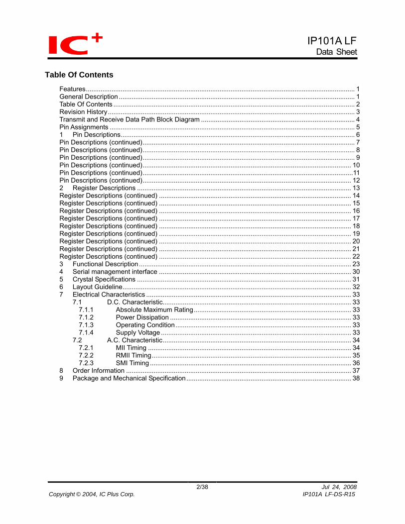
Table Of Contents
Features................................................................................................................................................... 1General Description ................................................................................................................................. 1Table Of Contents .................................................................................................................................... 2Revision History....................................................................................................................................... 3Transmit and Receive Data Path Block Diagram .................................................................................... 4Pin Assignments ...................................................................................................................................... 51 Pin Descriptions................................................................................................................................ 6Pin Descriptions (continued).................................................................................................................... 7Pin Descriptions (continued).................................................................................................................... 8Pin Descriptions (continued).................................................................................................................... 9Pin Descriptions (continued).................................................................................................................. 10Pin Descriptions (continued)...................................................................................................................11Pin Descriptions (continued).................................................................................................................. 122 Register Descriptions ..................................................................................................................... 13Register Descriptions (continued) ......................................................................................................... 14Register Descriptions (continued) ......................................................................................................... 15Register Descriptions (continued) ......................................................................................................... 16Register Descriptions (continued) ......................................................................................................... 17Register Descriptions (continued) ......................................................................................................... 18Register Descriptions (continued) ......................................................................................................... 19Register Descriptions (continued) ......................................................................................................... 20Register Descriptions (continued) ......................................................................................................... 21Register Descriptions (continued) ......................................................................................................... 223 Functional Description.................................................................................................................... 234 Serial management interface ......................................................................................................... 305 Crystal Specifications ..................................................................................................................... 316 Layout Guideline............................................................................................................................. 327 Electrical Characteristics ................................................................................................................ 33
7.1 D.C. Characteristic....................................................................................................... 337.1.1 Absolute Maximum Rating...................................................................................... 337.1.2 Power Dissipation ................................................................................................... 337.1.3 Operating Condition................................................................................................ 337.1.4 Supply Voltage ........................................................................................................ 33
7.2 A.C. Characteristic....................................................................................................... 347.2.1 MII Timing ............................................................................................................... 347.2.2 RMII Timing............................................................................................................. 357.2.3 SMI Timing .............................................................................................................. 36
8 Order Information ........................................................................................................................... 379 Package and Mechanical Specification.......................................................................................... 38
IP101A LFData Sheet
3/38 Jul 24, 2008Copyright © 2004, IC Plus Corp. IP101A LF-DS-R15
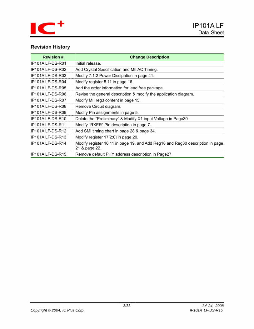
Revision History
Revision # Change Description IP101A LF-DS-R01 Initial release. IP101A LF-DS-R02 Add Crystal Specification and MII AC Timing. IP101A LF-DS-R03 Modify 7.1.2 Power Dissipation in page 41. IP101A LF-DS-R04 Modify register 5.11 in page 16. IP101A LF-DS-R05 Add the order information for lead free package. IP101A LF-DS-R06 Revise the general description & modify the application diagram. IP101A LF-DS-R07 Modify MII reg3 content in page 15. IP101A LF-DS-R08 Remove Circuit diagram. IP101A LF-DS-R09 Modify Pin assignments in page 5. IP101A LF-DS-R10 Delete the “Preliminary” & Modify X1 input Voltage in Page30 IP101A LF-DS-R11 Modify “RXER” Pin description in page 7. IP101A LF-DS-R12 Add SMI timing chart in page 28 & page 34. IP101A LF-DS-R13 Modify register 17[2:0] in page 20. IP101A LF-DS-R14 Modify register 16.11 in page 19, and Add Reg18 and Reg30 description in page
21 & page 22. IP101A LF-DS-R15 Remove default PHY address description in Page27

IP101A LFData Sheet
Transmit and Receive Data Path Block Diagram
4B/5B Encoder
Scrambler
Mux
Parallel to Serial
NRZI/MLT-3 Encoder
MII Registers
Auto-Negotiation
Parallel to Serial
NRZ/Manchester Encoder
4B/5B Decoder
Descrambler
Serial to Parallel
Clock Recovery
MLT3/NRZI Decoder
DSP Engine
Serial to Parallel
Manchester/NRZ
Decoder
Clock Recovery
Squelch
D/A & Line Driver
5B
5B
TXD MII/SNI/RMII Interface
RXD
RXITXO RJ-45 Connector
10Mbps
10Mbps
10Mbps
10Mbps
100Mbps
100Mbps
100Mbps
100Mbps
100Mbps
100Mbps 100Mbps 10Mbps
10Mbps
10Mbps
10Mbps
100Mbps
100Mbps
100Mbps
100Mbps
100Mbps
100Mbps 10Mbps
Figure 1: Flow chart of IP101A LF
Jul 24, 20084/38 Copyright © 2004, IC Plus Corp. IP101A LF-DS-R15

IP101A LFData Sheet
Pin Assignments
25. M
DC
26. M
DIO
33. M
DI_
TN
34. M
DI_
TP
28. I
SET
31. M
DI_
RP
30. M
DI_
RN
27.
TE
ST_O
N
32. R
EG
OU
T
36. A
VD
D33
29. A
GN
D
35. A
GN
D
IP101A LF
16. RX_CLK/ C50M_O
23. CRS /LEDMOD
22. RX_DV /CRS_DV
18. RXD3
19. RXD2
20. RXD1
21. RXD0
24. RX_ER
46. X1
47. X2
43. ISOL
40. RPTR
39. SPD
38. DPLX
37. AN_ENA
41. APS
44. MII_SNIB
13. LED3/ PHYAD3
15. LED4/ PHYAD4
42. RESET_N
48. INTR
45. DGND
14. DVDD33
17. DGNDFast Ethernet Single Phy Transceiver Chip48 pins LQFP package
7. T
X_C
LK
/
RE
F_C
LK
2. T
X_E
N
3. T
XD
3
4. T
XD
2
5. T
XD
1
6. T
XD
0
1. C
OL
/R
MII
9. L
ED
0/
PH
YA
D0
10. L
ED
1/
P
HY
AD
1
12. L
ED
2/
PH
YA
D2
8. R
EG
IN
11. D
GN
D
Figure 2 : IP101A LF pins assignment
Jul 24, 20085/38 Copyright © 2004, IC Plus Corp. IP101A LF-DS-R15

IP101A LFData Sheet
6/38 Jul 24, 2008Copyright © 2004, IC Plus Corp. IP101A LF-DS-R15
1 Pin Descriptions
Type Description LI Latched Input in power up or reset I/O Bi-directional input and output I Input O Output
Type Description PD Internal Pull-Down PU Internal Pull-Up P Power
OD Open Drain
Pin no. Label Type Description MII and PCS Interface - Management Interface Pins
25 MDC I Management Data Interface Clock: This pin provides a clock reference to MDIO. The clock rate can be up to 10MHz.
26 MDIO I/O Management Data interface Input/Output: The function of this pin is to transfer management information between PHY and MAC.
MII and PCS Interface – Media Independent Interface (MII) Pins 2 TX_EN I
(PD) Transmit Enable: This pin is an active high input. At high status, it indicates the nibble data in TXD[3:0] is valid.
7 TX_CLK O Transmit Clock: This pin provides a continuous 25MHz clock at 100BT and 2.5Mbps at 10BT as timing reference for TXD[3:0] and TX_EN when the chip operates under MII.
3, 4, 5, 6 TXD[3:0] I Transmit Data: When TX_EN is set high, MAC will transmit data through these 4 lines to PHY which the transmission is synchronizing with TX_CLK.
22 RX_DV O Receive Data Valid: At high status stands for data flow is present within RXD[0:3] lines and low means no data exchange occurred.
16 RX_CLK O Receive Clock: This pin provides 25MHz for 100BT or 2.5Mhz for 10BT and RX_DV pin uses this pin as its reference under MII.
18, 19, 20, 21
RXD[3:0] O Receive Data: These 4 data lines are transmission path for PHY to send data to MAC and they are synchronizing with RX_CLK.

IP101A LFData Sheet
7/38 Jul 24, 2008Copyright © 2004, IC Plus Corp. IP101A LF-DS-R15
Pin Descriptions (continued)
Pin no. Label Type Description MII and PCS Interface – Media Independent Interface (MII) Pins
24 RX_ER O (PD)
Receive error: This pin outputs a high status when errors occurred in the decoded data in the reception. (Notice: This pin is pulled down internally. An external 5.1KΩ
pull down resistor is needed to avoid the noise interference.) 1 COL/RMII O/LI
(PD) Collision Detected: When this pin outputs a high status signal it means collision is detected. RMII Mode: During power on reset, this pin status is latched and arranged with MII/SNIB (pin44) to determine MAC interface RMII MII/SNIB 1 X RMII Interface 0 1 MII Interface 0 0 SNI Interface (Notice: This pin is pulled down internally)
23 CRS/LEDMOD O (PD)
Carrier Sense: When signal output from this pin is high indicates the transmission or reception is in process and at low status means the line is in idle state. LEDMOD: During power on reset, this pin status is latched to determine at which LED mode to operate, please refer to the LED pins description. (Notice: This pin is pulled down internally)

IP101A LFData Sheet
8/38 Jul 24, 2008Copyright © 2004, IC Plus Corp. IP101A LF-DS-R15
Pin Descriptions (continued)
Pin no. Label Type Description RMII (Reduced MII)
7 REF_CLK I Reference Clock: This pin is an input pin operates as 50MHz reference clock (REF_CLK) in RMII mode.
16 C50M_O O Reference Clock out: This pin could be configured as 50MHz clock output in RMII mode. With 25MHz crystal/oscillator, IP101A LF could generate 50MHz output for RMII mode.
2 TX_EN I (PD)
Transmit Enable: For MAC to indicate transmit operation
5,6 TXD[1:0] I Transmit two-bit Data 24 RX_ER I/O Receive Error 22 CRS_DV O Carrier Sense and Receive Data Valid
20, 21 RXD[1:0] O Received two-bit Data SNI (Serial Network Interface): 10Mbps only
2 TX_EN I (PD)
Transmit Enable: Indicate transmit operation to MAC
7 TX_CLK O Transmit Clock: 10MHz, clock generated by PHY 6 TXD0 I Transmit Serial Data
16 RX_CLK O Receive Clock: 10MHz, clock recovery from received data 21 RXD0 O Received Serial Data 1 COL O Collision Detect
23 CRS O Carrier Sense Cable Transmission Interface
34 33
MDI_TP MDI_TN
I/O I/O
Transmit Output Pair: Differential pair shared by 100Base-TX and 10Base-T modes. When configured as 100Base-TX, output is an MLT-3 encoded waveform. When configured as 10Base-T, the output is Manchester code.
31 30
MDI_RP MDI_RN
I/O I/O
Receive Input Pair: Differential pair shared by 100Base-TX and 10Base-T modes.
IP101A LFData Sheet
9/38 Jul 24, 2008Copyright © 2004, IC Plus Corp. IP101A LF-DS-R15
Pin Descriptions (continued)
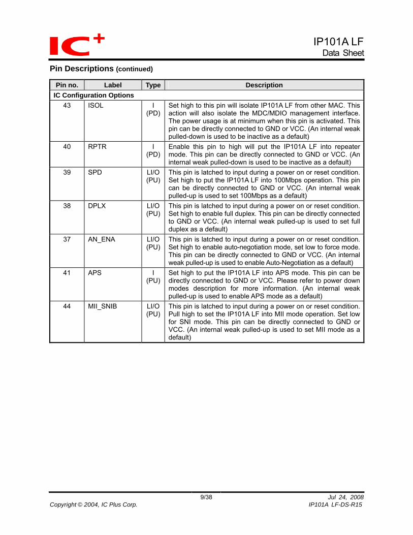
Pin no. Label Type Description IC Configuration Options
43 ISOL I (PD)
Set high to this pin will isolate IP101A LF from other MAC. This action will also isolate the MDC/MDIO management interface. The power usage is at minimum when this pin is activated. This pin can be directly connected to GND or VCC. (An internal weak pulled-down is used to be inactive as a default)
40 RPTR I (PD)
Enable this pin to high will put the IP101A LF into repeater mode. This pin can be directly connected to GND or VCC. (An internal weak pulled-down is used to be inactive as a default)
39 SPD LI/O (PU)
This pin is latched to input during a power on or reset condition. Set high to put the IP101A LF into 100Mbps operation. This pin can be directly connected to GND or VCC. (An internal weak pulled-up is used to set 100Mbps as a default)
38 DPLX LI/O (PU)
This pin is latched to input during a power on or reset condition. Set high to enable full duplex. This pin can be directly connected to GND or VCC. (An internal weak pulled-up is used to set full duplex as a default)
37 AN_ENA LI/O (PU)
This pin is latched to input during a power on or reset condition. Set high to enable auto-negotiation mode, set low to force mode. This pin can be directly connected to GND or VCC. (An internal weak pulled-up is used to enable Auto-Negotiation as a default)
41 APS I (PU)
Set high to put the IP101A LF into APS mode. This pin can be directly connected to GND or VCC. Please refer to power down modes description for more information. (An internal weak pulled-up is used to enable APS mode as a default)
44 MII_SNIB LI/O (PU)
This pin is latched to input during a power on or reset condition. Pull high to set the IP101A LF into MII mode operation. Set low for SNI mode. This pin can be directly connected to GND or VCC. (An internal weak pulled-up is used to set MII mode as a default)

IP101A LFData Sheet
10/38 Jul 24, 2008Copyright © 2004, IC Plus Corp. IP101A LF-DS-R15
Pin Descriptions (continued)
Pin no. Label Type Description LED and PHY Address Configuration These five pins are latched into the IP101A LF during reset to configure PHY address [4:0] used for MII management register interface. And then, in normal operation after initial reset, they are used as driving pins for status indication LED. The driving polarity, active low or active high, is determined by each latched status of the PHY address [4:0] during reset. If latched status is high then it will be active low, and if latched status is Low then it will be active high. Moreover, IP101A LF provides 2 LED operation modes. If 2nd LED mode is selected by pulling up pin CRS, only 4 LEDs are needed for status indication. Default is first LED mode.
LED mode 1 LED mode 2 LED0 LINK LINK /ACT(blinking) LED1 FULL DUPLEX FULL DUPLEX /COL(blinking) LED2 10BT /ACT(blinking) 10BT LED3 100BT /ACT(blinking) 100BT LED4 COL Reserved
9 PHYAD0/ LED0
LI/O PHY Address [0] Status: Mode1: Active when linked. Mode2: Active when linked and blinking when transmitting or receiving data.
10 PHYAD1/ LED1
LI/O PHY Address [1] Status: Mode1: Active when in Full Duplex operation. Mode2: Active when in Full Duplex operation and blinking when collisions occur.
12 PHYAD2/ LED2
LI/O PHY Address [2] Status: Mode1: Active when linked in 10Base-T mode, and blinking when transmitting or receiving data. Mode2: Active when linked in 10Base-T mode.
13 PHYAD3/ LED3
LI/O PHY Address [3] Status: Mode1: Active when linked in 100Base-TX and blinking when transmitting or receiving data. Mode2: Active when linked in 100Base-TX mode.
15 PHYAD4/ LED4
LI/O PHY Address [4] Status: Mode1: Active when collisions occur. Mode2: Reserved.
IP101A LFData Sheet
11/38 Jul 24, 2008Copyright © 2004, IC Plus Corp. IP101A LF-DS-R15
Pin Descriptions (continued)
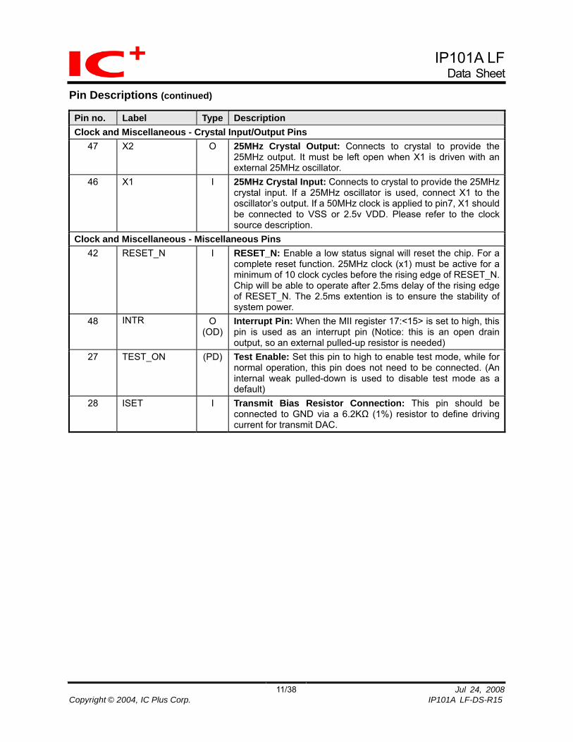
Pin no. Label Type Description Clock and Miscellaneous - Crystal Input/Output Pins
47 X2 O 25MHz Crystal Output: Connects to crystal to provide the 25MHz output. It must be left open when X1 is driven with an external 25MHz oscillator.
46 X1 I 25MHz Crystal Input: Connects to crystal to provide the 25MHz crystal input. If a 25MHz oscillator is used, connect X1 to the oscillator’s output. If a 50MHz clock is applied to pin7, X1 should be connected to VSS or 2.5v VDD. Please refer to the clock source description.
Clock and Miscellaneous - Miscellaneous Pins 42 RESET_N I RESET_N: Enable a low status signal will reset the chip. For a
complete reset function. 25MHz clock (x1) must be active for a minimum of 10 clock cycles before the rising edge of RESET_N. Chip will be able to operate after 2.5ms delay of the rising edge of RESET_N. The 2.5ms extention is to ensure the stability of system power.
48 INTR O (OD)
Interrupt Pin: When the MII register 17:<15> is set to high, this pin is used as an interrupt pin (Notice: this is an open drain output, so an external pulled-up resistor is needed)
27 TEST_ON (PD) Test Enable: Set this pin to high to enable test mode, while for normal operation, this pin does not need to be connected. (An internal weak pulled-down is used to disable test mode as a default)
28 ISET I Transmit Bias Resistor Connection: This pin should be connected to GND via a 6.2KΩ (1%) resistor to define driving current for transmit DAC.

IP101A LFData Sheet
12/38 Jul 24, 2008Copyright © 2004, IC Plus Corp. IP101A LF-DS-R15
Pin Descriptions (continued)
Pin no. Label Type Description Power and Ground
32 REGOUT P Regulator Power Output: This is a regulator power output for IP101A LF digital circuitry.
36 AVDD33 P 3.3V Analog power input: This is a 3.3V power supply for analog circuitry, and it should be decoupled carefully.
29,35 AGND P Analog Ground: These 2 pins should connect to motherboard’s GND.
8 REGIN P Regulator Power Input: This is a regulator power input from Pin32. No external regulator needed.
14 DVDD33 P 3.3V Digital Power input: This is a 3.3V power supply for digital circuitry.
11,17,45 DGND P Digital Ground: These 3 pins should connect to motherboard’s GND.

IP101A LFData Sheet
13/38 Jul 24, 2008Copyright © 2004, IC Plus Corp. IP101A LF-DS-R15
2 Register Descriptions
Bit Name Description/Usage Default value (h): 3100
Register 0 : MII Control Register 15 Reset When set, this action will bring both status and control
registers of the PHY to default state. This bit is self-clearing. 1 = Software reset 0 = Normal operation
0, RW
14 Loop-back This bit enables loop-back of transmit data to the receive data path, i.e., TXD to RXD. IP101A LF requires at least 512us to link after programming this bit. TX/RX packets should be activated after 512us. 1 = enable loop-back 0 = normal operation
0, RW
13 Speed Selection This bit sets the speed of transmission. 1 = 100Mbps 0 = 10Mbps
1, RW
12 Auto- Negotiation Enable
This bit determines the auto-negotiation function. 1 = enable auto-negotiation; bits 13 and 8 will be ignored. 0 = disable auto-negotiation; bits 13 and 0:<8> will determine the link speed and the data transfer mode, under this condition. Auto-MDIX function should be disabled (set Reg16.11=1) if this bit has been set to “0”. Please refer to section 3 Auto-MDIX function description for details.
1, RW (TP)
11 Power Down This bit will turn down the power of the PHY chip and the internal crystal oscillator circuit if this bit is enabled. The MDC and MDIO are still activated for accessing to the MAC. 1 = power down 0 = normal operation
0, RW
10 Isolate 1=electrically Isolate PHY from MII but not isolate MDC and MDIO 0=normal operation
0,RW
9 Restart Auto- Negotiation
This bit allows the auto-negotiation function to be reset. 1 = restart auto-negotiation 0 = normal operation
0, RW
8 Duplex Mode This bit sets the duplex mode if auto-negotiation is disabled (bit 12=0) 1 = full duplex 0 = half duplex After completing auto-negotiation, this bit will reflect the duplex status.(1: Full duplex, 0: Half duplex)
1, RW
7 Collision Test 1=enable COL signal test 0=disable COL signal test
0,RW
6:0 Reserved 0, RO

IP101A LFData Sheet
14/38 Jul 24, 2008Copyright © 2004, IC Plus Corp. IP101A LF-DS-R15
Register Descriptions (continued)
Bit Name Description/Usage Default value (h): 7849
Register 1 : MII Status Register 15 100Base-T4 1 = enable 100Base-T4 support
0 = suppress 100Base-T4 support 0, RO
14 100Base-TX Full Duplex
1 = enable 100Base-TX full duplex support 0 = suppress 100Base-TX full duplex support
1, RO
13 100BASE-TX Half Duplex
1 = enable 100Base-TX half duplex support 0 = suppress 100Base-TX half duplex support
1, RO
12 10Base-T Full Duplex
1 = enable 10Base-T full duplex support 0 = suppress 10Base-T full duplex support
1, RO
11 10_Base-T Half Duplex
1 = enable 10Base-T half duplex support 0 = suppress 10Base-T half duplex support
1, RO
10:7 Reserved 0, RO 6 MF Preamble
Suppression The IP101A LF will accept management frames with preamble suppressed. The IP101A LF accepts management frames without preamble. A Minimum of 32 preamble bits are required for the first SMI read/write transaction after reset. One idle bit is required between any two management transactions as per IEEE802.3u specifications
1, RO
5 Auto- Negotiation Complete
1 = auto-negotiation process completed 0 = auto-negotiation process not completed
0, RO
4 Remote Fault 1 = remote fault condition detected (cleared on read) 0 = no remote fault condition detected
0, RO/LH
3 Auto- Negotiation
1 = Link had not been experienced fail state 0 = Link had been experienced fail state
1, RO
2 Link Status 1 = valid link established 0 = no valid link established
0, RO/LL
1 Jabber Detect 1 = jabber condition detected 0 = no jabber condition detected
0, RO/LH
0 Extended Capability
1 = extended register capability 0 = basic register capability only
1, RO

IP101A LFData Sheet
15/38 Jul 24, 2008Copyright © 2004, IC Plus Corp. IP101A LF-DS-R15
Register Descriptions (continued)
Bit Name Description/Usage Default value (h): 0243
Register 2 : PHY Identifier Register 1 15:0 PHYID1 PHY identifier ID for software recognize IP101A LF 0X0243, RO
Bit Name Description/Usage Default value (h): 0C54
Register 3 : PHY Identifier Register 2 15:0 PHYID2 PHY identifier ID for software recognize 0X0C54, RO
Note : Register 2 and register 3 identifier registers altogether consist of Vender model, model revision number and Organizationally Unique identifier (OUI) information. Total of 32 bits allocate in these 2 registers and they can return all zeroes in all bits if desired. Register 2 contains OUI’s most significant bits and OUI’s least significant bits, Vender model, Model revision number are allocated in register 3.

IP101A LFData Sheet
16/38 Jul 24, 2008Copyright © 2004, IC Plus Corp. IP101A LF-DS-R15
Register Descriptions (continued)
Register 4 lists the advertised abilities during auto-negotiation for what will be transmitted to IP101A LF’s Link Partner.
Bit Name Description/Usage Default value (h): 0001
Register 4 : Auto-Negotiation Advertisement Register 15 NP Next Page bit.
0 = transmitting the primary capability data page 1 = transmitting the protocol specific data page
0, RO
14 Reserved 0, RO 13 RF 1 = advertise remote fault detection capability
0 = do not advertise remote fault detection capability 0, RW
12 Reserved 0, RO 11 Asymmetric.
Pause 1 = asymmetric flow control is supported by local node 0 = asymmetric flow control is NOT supported by local node
0, RW
10 Pause 1 = flow control is supported by local node 0 = flow control is NOT supported by local node
0, RW
9 T4 1 = 100Base-T4 is supported by local node 0 = 100Base-T4 not supported by local node
0, RO
8 TX Full Duplex 1 = 100Base-TX full duplex is supported by local node 0 = 100Base-TX full duplex not supported by local node
1, RW
7 TX 1 = 100Base-TX is supported by local node 0 = 100Base-TX not supported by local node
1, RW
6 10 Full Duplex 1 = 10Base-T full duplex supported by local node 0 = 10Base-T full duplex not supported by local node
1, RW
5 10 1 = 10Base-T is supported by local node 0 = 10Base-T not supported by local node
1, RW
4:0 Selector Binary encoded selector supported by this node. Currently only CSMA/CD <00001> is specified. No other protocols are supported.
<00001>, RO
IP101A LFData Sheet
17/38 Jul 24, 2008Copyright © 2004, IC Plus Corp. IP101A LF-DS-R15
Register Descriptions (continued)
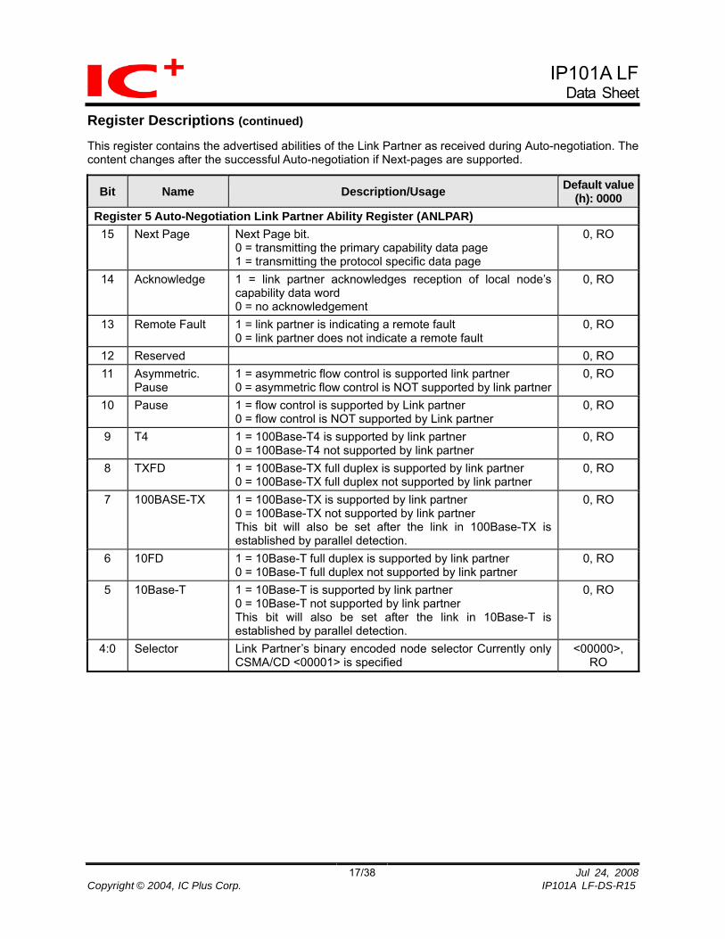
This register contains the advertised abilities of the Link Partner as received during Auto-negotiation. The content changes after the successful Auto-negotiation if Next-pages are supported.
Bit Name Description/Usage Default value (h): 0000
Register 5 Auto-Negotiation Link Partner Ability Register (ANLPAR) 15 Next Page Next Page bit.
0 = transmitting the primary capability data page 1 = transmitting the protocol specific data page
0, RO
14 Acknowledge 1 = link partner acknowledges reception of local node’s capability data word 0 = no acknowledgement
0, RO
13 Remote Fault 1 = link partner is indicating a remote fault 0 = link partner does not indicate a remote fault
0, RO
12 Reserved 0, RO 11 Asymmetric.
Pause 1 = asymmetric flow control is supported link partner 0 = asymmetric flow control is NOT supported by link partner
0, RO
10 Pause 1 = flow control is supported by Link partner 0 = flow control is NOT supported by Link partner
0, RO
9 T4 1 = 100Base-T4 is supported by link partner 0 = 100Base-T4 not supported by link partner
0, RO
8 TXFD 1 = 100Base-TX full duplex is supported by link partner 0 = 100Base-TX full duplex not supported by link partner
0, RO
7 100BASE-TX 1 = 100Base-TX is supported by link partner 0 = 100Base-TX not supported by link partner This bit will also be set after the link in 100Base-TX is established by parallel detection.
0, RO
6 10FD 1 = 10Base-T full duplex is supported by link partner 0 = 10Base-T full duplex not supported by link partner
0, RO
5 10Base-T 1 = 10Base-T is supported by link partner 0 = 10Base-T not supported by link partner This bit will also be set after the link in 10Base-T is established by parallel detection.
0, RO
4:0 Selector Link Partner’s binary encoded node selector Currently only CSMA/CD <00001> is specified
<00000>, RO

IP101A LFData Sheet
18/38 Jul 24, 2008Copyright © 2004, IC Plus Corp. IP101A LF-DS-R15
Register Descriptions (continued)
Register 6 defines more auto-negotiation registers to meet the requirement.
Bit Name Description/Usage Default value
(h): 0000
Register 6 : Auto-Negotiation Expansion Register 15:5 Reserved This bit is always set to 0. 0, RO
4 MLF This status indicates if a multiple link fault has occurred. 1 = fault occurred 0 = no fault occurred
0, RO
3 LP_NP_ABLE This status indicates if the link partner supports Next Page negotiation. 1 = supported 0 = not supported
0, RO
2 NP_ABLE This bit indicates if the device is able to send additional Next Pages.
0, RO
1 PAGE_RX This bit will be set if a new link code word page has been received. It is cleared automatically after the auto-negotiation link partner’s ability register (register 5) is read by the management.
0, RO
0 LP_NW_ABLE 1 = link partner supports auto-negotiation. 0, RO
IP101A LFData Sheet
19/38 Jul 24, 2008Copyright © 2004, IC Plus Corp. IP101A LF-DS-R15
Register Descriptions (continued)
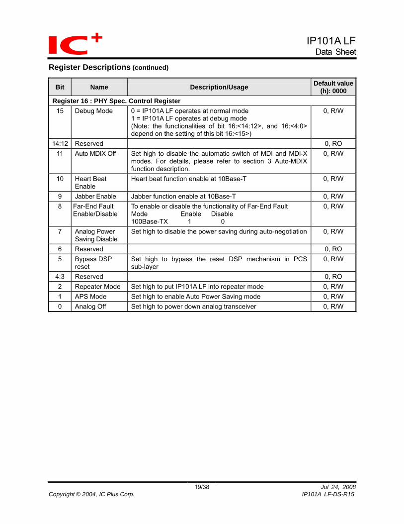
Bit Name Description/Usage Default value (h): 0000
Register 16 : PHY Spec. Control Register 15 Debug Mode 0 = IP101A LF operates at normal mode
1 = IP101A LF operates at debug mode (Note: the functionalities of bit 16:<14:12>, and 16:<4:0> depend on the setting of this bit 16:<15>)
0, R/W
14:12 Reserved 0, RO 11 Auto MDIX Off Set high to disable the automatic switch of MDI and MDI-X
modes. For details, please refer to section 3 Auto-MDIX function description.
0, R/W
10 Heart Beat Enable
Heart beat function enable at 10Base-T 0, R/W
9 Jabber Enable Jabber function enable at 10Base-T 0, R/W 8 Far-End Fault
Enable/Disable To enable or disable the functionality of Far-End Fault Mode Enable Disable 100Base-TX 1 0
0, R/W
7 Analog Power Saving Disable
Set high to disable the power saving during auto-negotiation 0, R/W
6 Reserved 0, RO 5 Bypass DSP
reset Set high to bypass the reset DSP mechanism in PCS sub-layer
0, R/W
4:3 Reserved 0, RO 2 Repeater Mode Set high to put IP101A LF into repeater mode 0, R/W 1 APS Mode Set high to enable Auto Power Saving mode 0, R/W 0 Analog Off Set high to power down analog transceiver 0, R/W

IP101A LFData Sheet
20/38 Jul 24, 2008Copyright © 2004, IC Plus Corp. IP101A LF-DS-R15
Register Descriptions (continued)
Bit Name Description/Usage Default value (h): 0E00
Register 17 : PHY Interrupt Ctrl/Status Register 15 INTR pin used Set high to enable pin48 as an interrupt pin. Pin48 will be
high impedance if this bit is set low. 0, R/W
14:12 Reserved 0, RO 11 All Mask When this bit is set high, changes in all events will not cause
an interrupt 1, R/W
10 Speed Mask When this bit is set high, changes in speed mode will not cause an interrupt
1, R/W
9 Duplex Mask When this bit is set high, changes in duplex mode will not cause an interrupt
1, R/W
8 Link Mask When this bit is set high, changes in link status will not cause an interrupt
1, R/W
7 Arbiter State Enable
When this bit is set low, changes in Auto-Negotiation arbiter state machine will not cause an interrupt
0, R/W
6 Arbiter State Change
Flag to indicate Auto-Negotiation arbiter change interrupt 0, RC
5:3 Reserved 0, RO 2 Speed Change Flag to indicate speed change interrupt 0, RC 1 Duplex Change Flag to indicate duplex change interrupt 0, RC 0 Link Status
Change Flag to indicate link status change interrupt 0, RC
IP101A LFData Sheet
21/38 Jul 24, 2008Copyright © 2004, IC Plus Corp. IP101A LF-DS-R15
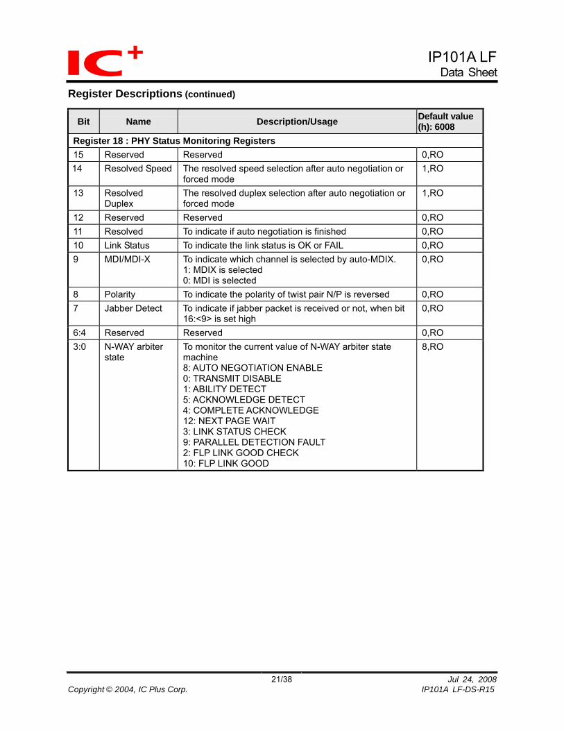
Register Descriptions (continued)
Bit Name Description/Usage Default value (h): 6008
Register 18 : PHY Status Monitoring Registers 15 Reserved Reserved 0,RO 14 Resolved Speed The resolved speed selection after auto negotiation or
forced mode 1,RO
13 Resolved Duplex
The resolved duplex selection after auto negotiation or forced mode
1,RO
12 Reserved Reserved 0,RO 11 Resolved To indicate if auto negotiation is finished 0,RO 10 Link Status To indicate the link status is OK or FAIL 0,RO 9 MDI/MDI-X To indicate which channel is selected by auto-MDIX.
1: MDIX is selected 0: MDI is selected
0,RO
8 Polarity To indicate the polarity of twist pair N/P is reversed 0,RO 7 Jabber Detect To indicate if jabber packet is received or not, when bit
16:<9> is set high 0,RO
6:4 Reserved Reserved 0,RO 3:0 N-WAY arbiter
state To monitor the current value of N-WAY arbiter state machine 8: AUTO NEGOTIATION ENABLE 0: TRANSMIT DISABLE 1: ABILITY DETECT 5: ACKNOWLEDGE DETECT 4: COMPLETE ACKNOWLEDGE 12: NEXT PAGE WAIT 3: LINK STATUS CHECK 9: PARALLEL DETECTION FAULT 2: FLP LINK GOOD CHECK 10: FLP LINK GOOD
8,RO

IP101A LFData Sheet
22/38 Jul 24, 2008Copyright © 2004, IC Plus Corp. IP101A LF-DS-R15
Register Descriptions (continued)
Bit Name Description/Usage Default value (h): 0002
Register 30 : PHY Spec. Control Registers 15:4 Reserved Reserved
Force to 0, in application. Any change of this bit is not recommend.
0, RW
3 FORCE_MDIX Set high to force the MDIX channel to be selected. 1: Force the MDIX channel to be selected. 0: MDI channel is selected when auto-MDIX is turned off. When IP101A LF operates in Force 10Mb mode or APS mode, this bit is not able to write.
0, RW
2 Reserved Reserved Force to 0, in application. Any change of this bit is not recommend.
0, RW
1 Reserved Reserved Force to 1, in application. Any change of this bit is not recommend.
1, RW
0 Reserved Reserved Force to 0, in application. Any change of this bit is not recommend.
0, RW
IP101A LFData Sheet
23/38 Jul 24, 2008Copyright © 2004, IC Plus Corp. IP101A LF-DS-R15
3 Functional Description
IP101A LF 10/100Mbps Ethernet PHY Transceiver integrates 100 Base-TX and 10 Base-T modules into a single chip. IP101A LF acts as an interface between physical signaling and Media Access Controller (MAC). IP101A LF has several major functions: 1. PCS layer (Physical Coding Sub-Layer): This function contains transmit, receive and carrier sense
functional circuitries. 2. Management interface: Media Independent Interface (MII) or Reduced Management Interface (RMII)
registers contains information for communication with other MAC. 3. Auto-Negotiation: Communication conditions between 2 PHY transceivers. IP101A LF advertise its
own ability and also detects corresponding operational mode from the other party, eventually both sides will come to an agreement for their optimized transmission mode.
IP101A LF’s major features included: 1. Flow Control ability 2. LED configuration access 3. Operation modes for both full and half duplex 4. APS (Auto Power Saving) mode 5. Base Line Wander (BLW) compensation 6. Auto MDI/MDIX function 7. Interrupt function 8. Repeater Mode 9. Flexible clock source Major Functional Block Description The functional blocks diagram is referred to Figure 1: 1. 4B/5B encoder: 100 Base-X transmissions require converting 4-bit nibble data into 5-bit wide data
code-word format. Transmitting data is packaged by J/K codes at the start of packet and by T/R codes at the end of packet in the 4B/5B block. When transmit error has occurred during a transmitting process, the H error code will be sent. The idle code is sent between two packets.
2. 4B/5B Decoder: The decoder performs the 5B/4B decoding from the received code-groups. The 5
bits (5B) data is decoded into four bits nibble data. The decoded 4 bit (4B) data is then forwarded through MII to the repeater, switch or MAC device. The SSD is then converted into 4B 5 nibbles and the ESD and IDLE Codes are replaced by 4B 0 nibbles data. The decoded data is driven onto the corresponding MII port or shared MII port. Receiving an invalid code group will cause PHY to assert the MII RXER signal.
3. Scrambler/Descrambler: Repetitive patterns exist in 4B/5B encoded data which result in large RF
spectrum peaks and keep the system from being approved by regulatory agencies. The peak in the radiated signal is reduced significantly by scrambling the transmitted signal. Scrambler adds a random generator to the data signal output. The resulting signal is with fewer repetitive data patterns. The scrambled data stream is descrambled at the receiver by adding another random generator to the output. The receiver’s random generator has the same function as the transmitter’s random generator. Scrambler operation is dictated by the 100Base-TX and TP_FDDI standards.
4. NRZI/MLT-3(Manchester) Encoder and Decoder: 100Base-TX Transmission requires to encode the
data into NRZ format and again converted into MLT-3 signal, while 10 Base-T will convert into Manchester form after NRZ coding. This helps to remove the high frequency noise generated by the twisted pair cables. At receiving end, the coding is reversed from MLT-3 (Manchester) signal back to

IP101A LFData Sheet
24/38 Jul 24, 2008Copyright © 2004, IC Plus Corp. IP101A LF-DS-R15
NRZ format. 5. Clock Recovery: The receiver circuit recovers data from the input stream by regenerating clocking
information embedded in the serial stream. The clock recovery block extracts the RXCLK from the transition of received
6. DSP Engine: This block includes Adaptive equalizer and Base Line Wander correction function. Transmission Description
10Mbps Transmit flow path:
TXD Parallel to Serial NRZI/Manchester Encoder D/A & line driver TXO
After MAC passes data to PHY via 4 bits nibbles, the data are serialized in the parallel to serial converter. The converter outputs NRZI coded data which the data are then mapped to Manchester code within the Manchester Encoder. Before transmitting to the physical medium, the Manchester coded data are shaped by D/A converter to fit the physical medium. 10Mbps Receive:
RXI Squelch Clock Recovery Manchester/NRZ Decoder Serial to Parallel RXD
The squelch block determines valid data from both AC timing and DC amplitude measurement. When a valid data is present in the medium, squelch block will generate a signal to indicate the data has received. The data receive are coded in Manchester form, and are decoded in the Manchester to NRZ Decoder. Then the data are mapped to 4 bits nibbles and transmitted onto MAC interface. 100Mbps TX Transmit:
TXD 4B/5B Encoder Scrambler Mux Parallel to Serial NRZI/MLT-3 Encoder D/A & line driver TXO
The major differences between 10Mbps transmission and 100Mbps transmission are that 100Mbps transmission requires to be coded from 4-bit wide nibbles to 5 bits wide data coding, and after that the data are scrambled through scrambler to reduce the radiated energy generated by the 4B/5B conversion. Then the data is converted into NRZI form and again from NRZI coded form into MLT-3 form. The MLT-3 data form is fed into D/A converter and shaped to fit the physical medium transmission. 100Mbps RX Receive:
RXI DSP MLT-3/NRZI Decoder Clock Recovery Serial to Parallel Descrambler 4B/5B Decoder RXD
The received data first go through DSP engines which includes adaptive equalizer and base-line wander correction mechanism. The adaptive equalizer will compensate the loss of signals during the transmission, while base-line wander monitors and corrects the equalization process. If a valid data is detected then the data are parallelized in Serial to Parallel block, which it converts NRZI coded data form back to scrambled data. The scrambled data are descrambled and converted back to 4 bits–wide format data and then feed into MAC. MII and Management Control Interface
Media Independent Interface (MII) is described in clause 22 in the IEEE 802.3u standard. The main function of this interface is to provide a communication path between PHY and MAC/Repeater. It can operate either in 10Mbps or 100Mbps environment, and operate at 2.5MHz frequency for 10Mbps clock data rate or 25MHz frequency for 100Mbps data rate transmission. MII consists of 4 bit wide data path for both transmit and receive. The transmission pins consists of TXD[3:0], TX_EN and TXC, and at receiving MII pins have RXD[3:0], RXER, RX_DV and RXC. The Management control pins include MDC and MDIO.

IP101A LFData Sheet
25/38 Jul 24, 2008Copyright © 2004, IC Plus Corp. IP101A LF-DS-R15
MDC, Management Data Clock, provides management data clock at maximum of 10MHz as a reference for MDIO, Management Data Input/Output. CRS, Carrier Sense, is used for signaling data transmission is in process while COL, Collision, is used for signaling the occurrence of collision during transmission. Transmitting a packet, MAC will first assert TX_EN and convert the information into 4 bit wide data and then pass the data to IP101A LF. IP101A LF will sample the data according to TX_CLK until TX_EN is low. While receiving a packet, IP101A LF asserts RX_DV high when data present in the medium through RXD[3:0] bus lines. IP101A LF samples received data according to RX_CLK until the medium is back to idle state. RMII Interface
Reduced Media Independent Interface (RMII) is defined to provide a fewer pins data transmission condition. The management interface, MDC and MDIO, are identical to the MII defined in IEEE 802.3. RMII supports 10/100Mb data rates and the clock source is provided by a single 50MHz clock from either external or within IP101A LF. This clock is used as reference for transmit, receive and control. RMII provides independent 2 bit wide transmit and receive data path, i.e., TXD[1:0] and RXD[1:0]. CRS_DV is asserted when the receive medium is not idle and de-asserted when the medium is idle. Before any transmission occurs, CRS_DV should be de-asserted and value “00” should be present in both TXD[1:0] and RXD[1:0]. When transmission begins, IP101A LF will send “01” (TXD[1:0] = 01) for preamble to indicate SFD, and also assert TX_EN synchronous with first nibble of the preamble. TX_EN should be de-asserted until the end of the data transmission. At receiving mechanism, by receiving “01” means a valid data is available. If False carrier is detected, RXD[1:0] shall be “10” until the end of the transmission. At 10Mbps mode, every 10th cycle of REF_CLK will be sampled in RXD[1:0] and TXD[1:], because the REF_CLK frequency is 10 times faster than the data rate of the 10Mbps. SNI Interface
The IP101A LF also provides serial-network interface for legacy MACs, when the chip operates at 10BASE-T either by Auto-Negotiation resolved result or by forced mode. To setup for this mode of operation, pull both the MII/SNIB and the COL/RMII pins to low. The transaction protocol of SNI interface is almost identical to that of MII interface, except of data bit width and clock rate. This interface consists of 10Mbps transmit and receive clock generated by PHY’s digital phase-locked loop (DPLL), 10Mbps transmit and receive serial data, transmit enable, collision detect, and carry sense signals.

IP101A LFData Sheet
26/38 Jul 24, 2008Copyright © 2004, IC Plus Corp. IP101A LF-DS-R15
Auto-Negotiation and Related Information
IP101A LF supports clause 28 in the IEEE 802.3u standard. IP101A LF can be operated either in 10Mbps/100Mbps or half/full duplex transmission mode. IP101A LF also supports flow control mechanism to prevent any collision in the network. If the other end does not support Auto-Negotiation function, IP101A LF will link at half duplex mode and enter parallel detection. At beginning of auto-negotiation, IP101A LF will advertise its own ability by sending FLP waveform out to the other end and also listening signals from the other end. IP101A LF will place itself into correct connection speed depends on the received signals. If NLP signal is replied from the other end, IP101A LF will enter 10Mbps, while active idle pulses (unique 100Mbps pattern) IP101A LF will go to 100Mbps mode instead. Once the negotiation has completed with the other party, IP101A LF will configure itself to the desired connection mode, i.e., 10/100Mbps or Half/Full duplex modes. If there is no detection of link pulses within 1200~1500ms, IP101A LF will enter Link Fail State and restart auto-negotiation procedure. The auto-negotiation information is stored in the IP101A LF’s MII registers. These registers can be modified and monitor the IP101A LF’s Auto-Negotiation status. The reset auto-negotiation in register 0 of MII registers can be set at any time to restart auto-negotiation. The flow control ability is also included in the IP101A LF chip. If MAC supports flow control condition, then flow control will be enabled by setting bit 10 (Pause) of the Register 4. Pin 37 (AN_ENA), 38 (DLPX), 39 (SPD) can be configured manually to set IP101A LF’s transmission ability. 1. Enabling Pin 37 (set high) will put IP101A LF to Auto-Negotiation mode, if set low to pin 37, it will put
IP101A LF into forced mode. 2. Pin 38 will configure Duplex ability of IP101A LF, at high, IP101A LF is set to Full-Duplex and low will
let IP101A LF enter half duplex mode. 3. Pin 39 determines the speed of connection. If the pin is pulled high, IP101A LF is set at 100Mbps,
while at low will make IP101A LF to connect at 10Mbps speed.
AN_ENA (Pin 37)
DLPX (Pin38)
SPD (Pin39) Operation
H L L Auto-Negotiation enable, the ability field does not support 100Mbps and full duplex mode operation
H H L Auto-Negotiation enable, the ability field does not support 100Mbps operation
H L H Auto-Negotiation enable, the ability field does not support full duplex mode operation
H H H Default setup, auto-negotiation enable, the IP101A LF will support 10BT/100BT, half/full duplex mode operation
L L L Auto-Negotiation disable, force the IP101A LF into 10BT and half duplex mode.
L H L Auto-Negotiation disable, force the IP101A LF into 10BT and full duplex mode.
L L H Auto-Negotiation disable, force the IP101A LF into 100BT and half duplex mode.
L H H Auto-Negotiation disable, force the IP101A LF into 100BT and full duplex mode.

IP101A LFData Sheet
Auto MDIX function IP101A LF will keep sensing incoming signal in MDI RX pair, if no incoming signal is detected, IP101A LF will switch TX and RX pairs automatically trying to establish connection. IP101A LF supports this function both in Auto-Negotiation mode and force mode. LED Configuration
IP101A LF provides 2 LED operation modes, Mode 1 (default):
LED Function LED0 Link status: Active indicates the link has established LED1 Duplex operation: Active indicates full duplex LED2 10BT/ACT: Active indicates 10Mbps connection has established, and blinking while
TX/RX events occur. LED3 100BT/ACT: Active indicates 100Mbps connection has established, and blinking
while TX/RX events occur. LED4 Collision detect: Active indicates Collision has occurred
Mode 2 (could be set by pulling up CRS with a 4.7K resistor):
LED Function LED0 Link/ACT: Active indicates the link has established, and blinking while TX/RX events
occur. LED1 Duplex/COL: Active indicates full duplex, and blinking while collision events occur. LED2 10BT: Active indicates 10Mbps connection has established LED3 100BT: Active indicates 100Mbps connection has established LED4 Reserved.
LED pins also include the information of PHY address. The PHY address can be modified by changing the LED circuitry. The modification can be arranged as follow:
27/38 Jul 24, 2008Copyright © 2004, IC Plus Corp. IP101A LF-DS-R15
LEDx X=0:4 R26 510 ohm
R27 5.1k ohm
VDD33
D6
LED
R27
5.1k ohm
D6 LED LEDx X=0:4
R26
510 ohm
Figure 3: PHY address Configuration The left diagram will enable the specific PHY address to 1, if it is connected to VDD33. The diagram on the right shows the configuration for setting PHY address to 0, when the circuit is connected to ground. By setting either one of the bits according to the diagram will allow one to modify PHY addresses from PHYAD0 to PHYAD4.

IP101A LFData Sheet
Flexible Clock Source
Pin1 COL/RMII
Pin44 MII/SNIB
Function
1 1 RMII, ext 50MHz osc clk in to pin7 1 0 RMII, 25MHz crystal or osc from X1,X2; 50MHz clk out to pin16. (Please refer
to the following figure for our recommened application circuit.) 0 1 MII, 25MHz crystal or osc from X1,X2 0 0 SNI, 25MHz crystal or osc from X1,X2
While pin1=1 and pin44=0 has been selected, 50MHz clock will be provided by IP101A LF in RMII mode. We suggest the application circuit as the following :
Buffer
IP101A
25M
Other PHY
CPU/Switch/MAC
Pin16Pin7
Pin46Pin47
50MHz colck
For this configuration, RMII reference clock for IP101A LF is from pin7. Clock skew could be eliminated by adding an external buffer and placing equal trace lengths between buffer outputs and each chip.
Jul 24, 200828/38 Copyright © 2004, IC Plus Corp. IP101A LF-DS-R15

IP101A LFData Sheet
29/38 Jul 24, 2008Copyright © 2004, IC Plus Corp. IP101A LF-DS-R15
Power-Down Modes
IP101A LF can be power-down by 4 methods. These 4 methods are as follow: Power Down in bit 11 of Register 0: Enable this bit will disconnect the power to IP101A LF and also internal clock, but MDC and MDIO are still activated. APS mode in bit 1 of Register 16: Set high to this bit will set PHY into power saving mode(APS sleeping mode) while link is down, MDC and MDIO are kept activated. IP101A LF will send NLP every 64ms during APS sleeping mode. Analog off in bit 0 of Register 16: Enable this bit will put IP101A LF in analog off state. This will power down all analog functions but internal 25MHz operating clock is active, and MDC and MDIO are also activated. ISOL pin (pin 43): Set high will isolate IP101A LF from MAC and disable management interface (MDC and MDIO). The power usage is at minimum when this pin is activated. Repeater Modes
To enter Repeater mode, one can either set pin 40 (RPTR) to high or set 1 to bit 2 of Register 16 will allow IP101A LF to enter Repeater mode. If IP101A LF is used in repeater, CRS will be high if IC is in process of receiving packets, while IP101A LF is used in a network interface card, CRS will be generated in both transmitting and receiving packets. Miscellaneous
ISET (pin 28) should be connected to GND via a 6.2k ohm resistor with 1% accuracy to ensure a correct driving current for transmit DAC. Set low to pin 42, REST_N, for at least 10ms will reset all functions available in IP101A LF. The bit 15 of Register 0 will put PHY into its default status. Interrupt
IP101A LF provides 4 kinds of interrupt function: speed change, duplex change, link change and arbiter state change. Interrupt masks could be selected by Reg 17, and an active low interrupt will be sent from pin48 when event occurs.

IP101A LFData Sheet
4 Serial management interface
User can access IP101A LF’s MII registers through serial management interface MDC and MDIO. A specific pattern on MDIO is used to access a MII register. Its format is shown in the following table. When the SMI is idle, MDIO is in high impedance. To initialize the MDIO interface, the management entity sends a sequence of 32 contiguous “1” and “start” on MDIO.
Frame format
<Idle><start><op code><IP101A LF’s address><Registers address><turnaround> <data><idle>
Read Operation
<Idle><01><10><A4A3A2A1A0><R4R3R2R1R0><Z0> <b15 b14 b13 b12 b11 b10 b9 b8 b7 b6 b5 b4 b3 b2 b1b0><Idle>
Write Operation
<Idle><01><01><A4A3A2A1A0><R4R3R2R1R0><10> <b15 b14 b13 b12 b11 b10 b9 b8 b7 b6 b5 b4 b3 b2 b1b0><Idle>
000000001100110001000001000010101..1
idle start opcode
PHY address =01h
Reg address =00h
TA
Register data
b15
b14
b13
b12
b11
b10
b9
b8
b7
b6
b5
b4
b3
b2
b1
b0
idleA4
A3
A2
A1
A0
R4
R3
R2
R1
R0
write
zz
00000000100011000Z00000100000110
idle start opcode
PHY address =01h
Reg address =00h
TA
Register data
b15
b14
b13
b12
b11
b10
b9
b8
b7
b6
b5
b4
b3
b2
b1
b0
idleA4
A3
A2
A1
A0
R4
R3
R2
R1
R0
read
zz z
MDC
MDIO
MDC
MDIO
1..1
1..1
1..1
Jul 24, 200830/38 Copyright © 2004, IC Plus Corp. IP101A LF-DS-R15
IP101A LFData Sheet
31/38 Jul 24, 2008Copyright © 2004, IC Plus Corp. IP101A LF-DS-R15
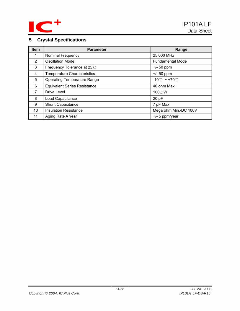
5 Crystal Specifications
Item Parameter Range 1 Nominal Frequency 25.000 MHz 2 Oscillation Mode Fundamental Mode 3 Frequency Tolerance at 25 +/- 50 ppm 4 Temperature Characteristics +/- 50 ppm 5 Operating Temperature Range -10 ~ +70 6 Equivalent Series Resistance 40 ohm Max. 7 Drive Level 100μW 8 Load Capacitance 20 pF 9 Shunt Capacitance 7 pF Max
10 Insulation Resistance Mega ohm Min./DC 100V 11 Aging Rate A Year +/- 5 ppm/year

IP101A LFData Sheet
32/38 Jul 24, 2008Copyright © 2004, IC Plus Corp. IP101A LF-DS-R15
6 Layout Guideline
General Layout Guideline
Best performance depends on good layout. The following recommendation steps will help customer to gain maximum performance. Create good power source to minimize noise from switching power source.
All components are qualified, especially high noise component, such as clock component. Use bulk capacitors between power plane and ground plane for 4 layers board, signals trace on
component and bottom side, power plane on third layer, and ground layer on second layer. Use decoupling capacitors to decouple high frequency noise between chip’s power and ground,
must be as close as possible to IP101A LF. The clock trace length to IP101A LF must be equal the clock trace length to MAC. Use guard traces to protect clock traces if possible Avoid signals path parallel to clock signals path, because clock signals will interference with other
parallel signals, degrading signal quality, such as MDC and X1signals. The clock must be low jitter with less than 0.5ns for 25/50/125Mhz 100ppm. Avoid highly speed signal across ground gap to prevent large EMI effect. Keep ground region as one continuous and unbroken plane. Place a gap between the system and chassis grounds. No any ground loop exists on the chassis ground.
Twisted Pair recommendation
When routing the TD+/- signal traces from IP101A LF to transformer, the traces should be as short as possible, the termination resistors should be as close as possible to the output of the TD+/- pair of IP101A LF. Center tap of primary winding of these transformers must be connected to analog 2.5V respectively. It is recommended that RD+/- trace pair be route such that the space between it and others is three times space, which can separate individual traces from one another. It is recommended that offers chassis ground in the area between transformer and media connector (RJ-45 port), this isolates the analog signals from external noise sources and reduces EMI effect. Note the usage of the vias, it is best not use via to place anywhere other than in close proximity to device, in order to minimize impedance variations in a given signal trace.
IP101A LFData Sheet
33/38 Jul 24, 2008Copyright © 2004, IC Plus Corp. IP101A LF-DS-R15
7 Electrical Characteristics
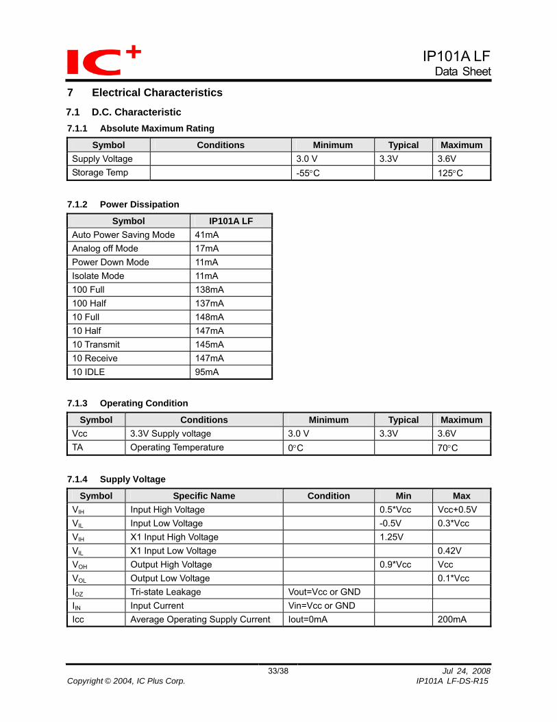
7.1 D.C. Characteristic 7.1.1 Absolute Maximum Rating
Symbol Conditions Minimum Typical MaximumSupply Voltage 3.0 V 3.3V 3.6V Storage Temp -55°C 125°C
7.1.2 Power Dissipation
Symbol IP101A LF Auto Power Saving Mode 41mA Analog off Mode 17mA Power Down Mode 11mA Isolate Mode 11mA 100 Full 138mA 100 Half 137mA 10 Full 148mA 10 Half 147mA 10 Transmit 145mA 10 Receive 147mA 10 IDLE 95mA
7.1.3 Operating Condition
Symbol Conditions Minimum Typical MaximumVcc 3.3V Supply voltage 3.0 V 3.3V 3.6V TA Operating Temperature 0°C 70°C
7.1.4 Supply Voltage
Symbol Specific Name Condition Min Max VIH Input High Voltage 0.5*Vcc Vcc+0.5V VIL Input Low Voltage -0.5V 0.3*Vcc VIH X1 Input High Voltage 1.25V VIL X1 Input Low Voltage 0.42V VOH Output High Voltage 0.9*Vcc Vcc VOL Output Low Voltage 0.1*Vcc IOZ Tri-state Leakage Vout=Vcc or GND IIN Input Current Vin=Vcc or GND Icc Average Operating Supply Current Iout=0mA 200mA
IP101A LFData Sheet
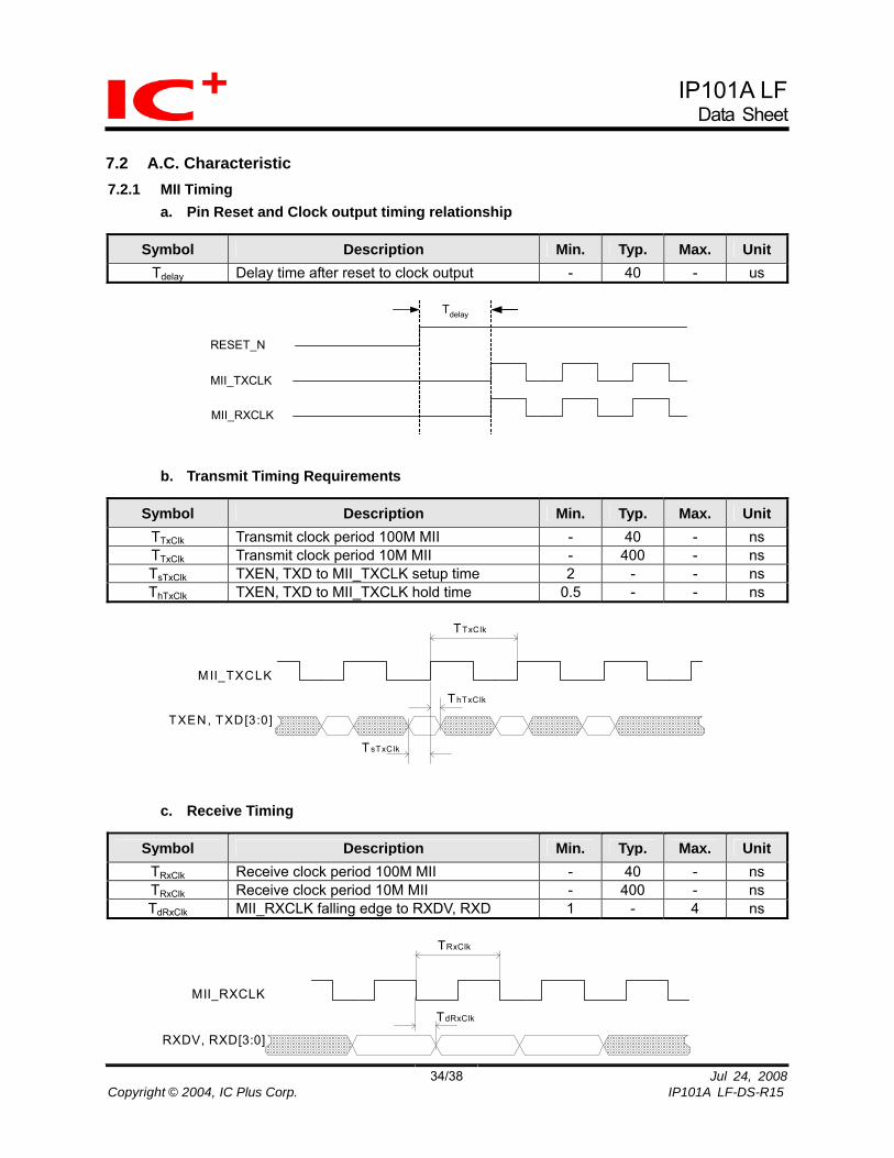
7.2 A.C. Characteristic 7.2.1 MII Timing
a. Pin Reset and Clock output timing relationship
Symbol Description Min. Typ. Max. Unit Tdelay Delay time after reset to clock output - 40 - us
MII_TXCLK
MII_RXCLK
Tdelay
RESET_N
b. Transmit Timing Requirements
Symbol Description Min. Typ. Max. Unit TTxClk Transmit clock period 100M MII - 40 - ns TTxClk Transmit clock period 10M MII - 400 - ns TsTxClk TXEN, TXD to MII_TXCLK setup time 2 - - ns ThTxClk TXEN, TXD to MII_TXCLK hold time 0.5 - - ns
M II_TXCLK
TXEN, TXD[3:0]
T sTxClk
ThTxClk
TTxClk
c. Receive Timing
Symbol Description Min. Typ. Max. Unit TRxClk Receive clock period 100M MII - 40 - ns TRxClk Receive clock period 10M MII - 400 - ns TdRxClk MII_RXCLK falling edge to RXDV, RXD 1 - 4 ns
TdRxClk
MII_RXCLK
RXDV, RXD[3:0]
TRxClk
Jul 24, 200834/38 Copyright © 2004, IC Plus Corp. IP101A LF-DS-R15

IP101A LFData Sheet
7.2.2 RMII Timing
a. Pin Reset and Clock output timing relationship (If pin 16 has been configured as 50MHz output )
Symbol Description Min. Typ. Max. Unit Tdelay Delay time after reset to clock output - 40 - us
C50M_O
Tdelay
RESET_N
b. Clock Timing RMII
Symbol Description Notes Min Typ Max UnitsTR_CLKRMII REFCLK Rise time VIL (max) to VIH (min) - - 3.0 ns TF_CLKRMII REFCLK Fall time VIH (min) to VIL (max) - - 3.0 ns TP_CLKRMII REFCLK Period 20.0 ± 50
ppm ns
TH_CLKRMII REFCLK High 8.0 10.0 12.0 ns TL_CLKRMII REFCLK Low 8.0 10.0 12.0 ns
T P_CLKRMII
T H_CLKRMII T L_CLKRMII
T R_CLKRMII T F_CLKRMII
REFCLK
V IH
V IL
Figure 4: Clock Timing RMII
c. RMII Receive Timing
Symbol Description Notes Min Typ Max UnitsTDLY_RXD REFCLK rising edge
to RXD[1:0], RX_ER and CRS_DV delay
Initial rising edge of CRS_DV is asynchronous to REFCLK
12.0 15.0 ns
TR_RXD RXD[1:0], RX_ER, CRS_DV Rise time
VIL (max) to VIH (min) 1.0 2.5 ns
TF_RXD RXD[1:0], RX_ER, CRS_DV Fall time
VIH (min) to VIL (max) 1.0 2.5 ns
Jul 24, 200835/38 Copyright © 2004, IC Plus Corp. IP101A LF-DS-R15

IP101A LFData Sheet
CRS_DV
RXD[1:0]RX_ER
REFCLK
T DLY_RXD
Figure 5: Receive Delay
T R_RXD T F_RXD
CRS_DV
RXD[1:0]RX_ER
V IH_DIG(MAX)
V IL_DIG(MAX)
Figure 6: RMII Rise and Fall Times
d. RMII Transmit Timing
Symbol Parameter Min Typ Max UnitsTSU_TXD_RMII TXD[1:0], TX_EN, Data Setup to REFCLK rising
edge 4.0 ns
THD_TXD_RMII TXD[1:0], TX_EN, Data Hold from REFCLK rising edge
2.0 ns
TX[1:0]TX_EN
REFCLK
T HD_TXD_RMIIT SU_TXD_RMII
Valid Data
Figure 7: RMII Transmit Timing
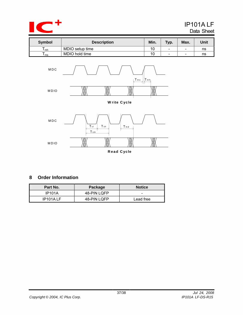
7.2.3 SMI Timing
a. MDC/MDIO Timing
Symbol Description Min. Typ. Max. Unit Tch MDC High Time 40 - - ns Tcl MDC Low Time 40 - - ns Tcm MDC period 80 - - ns Tmd MDIO output delay - - 5 ns
Jul 24, 200836/38 Copyright © 2004, IC Plus Corp. IP101A LF-DS-R15
IP101A LFData Sheet
37/38 Jul 24, 2008Copyright © 2004, IC Plus Corp. IP101A LF-DS-R15
Symbol Description Min. Typ. Max. Unit Tmh MDIO setup time 10 - - ns Tms MDIO hold time 10 - - ns
M D C
M D IO
T m s T m h
W rite C yc le
T cl T ch
T cm
T m d
M D C
M D IO
R e a d C yc le
8 Order Information
Part No. Package Notice IP101A 48-PIN LQFP -
IP101A LF 48-PIN LQFP Lead free

IP101A LFData Sheet
9 Package and Mechanical Specification
FSEATINGPLANE
1
12
13 24
25
36
3748
HE
PH
E
12"
12" cbeD F y
1
12
13 24
25
36
3748
2
2AA2
A1LL1
0.25
4GAUGE PLANE
DETAIL "E"
D
"E"
θ
mm inch
AA1
1.600MAX.
A20.050~0.150
0.0630MAX.
b1.400 0.05
0.0020~0.0059
c0.200TYP
0.0551 0.0020
D0.127TYP
0.0078TYP
Ee
Hd0.500TYP
0.0050TYP
unitSymbol
yL1L
He
0"~7"0.100MAX.1.000REF
0.600 0.150
0"~7"0.0039MAX.0.0393REF
0.0236 0.006
0.0196TYP
+- +-
0.2756 0.0039+-7.000 0.100+-7.000 0.100+- 0.2756 0.0039+-
+- +-
9.000 0.250 0.3543 0.0098+- +-9.000 0.250 0.3543 0.0098+- +-
Notes:1. DIMENSION D & E DO NOT INCLUDE MOLD FLASH OR PROTRUSION.2. DIMENSION b DOES NOT INCLUDE DAMBAR PROTRUSION / INTRUSION.3. MAX. END FLASH IS 0.15MM.4. MAX. DAMBAR PROTRUSION IS 0.13MM.GENERAL APPEARANCE SPEC SHOULD BE BASED ON FINAL VISUAL INSPECTION SPEC.
IC Plus Corp. Headquarters Sales Office 10F, No.47, Lane 2, Kwang-Fu Road, Sec. 2, 4F, No. 106, Hsin-Tai-Wu Road, Sec.1, Hsin-Chu City, Taiwan 300, R.O.C. Hsi-Chih, Taipei Hsien, Taiwan 221, R.O.C. TEL : 886-3-575-0275 FAX : 886-3-575-0475 TEL : 886-2-2696-1669 FAX : 886-2-2696-2220 Website : www.icplus.com.tw
Jul 24, 200838/38 Copyright © 2004, IC Plus Corp. IP101A LF-DS-R15