skywire 4g lte cat m1 w/ gnss embedded cellular modem ... · serial communications 11 ... x3...
TRANSCRIPT

Skywire 4G LTE Cat M1 w/ GNSS Embedded Cellular Modem Datasheet NimbeLink Corp Updated: January 2018
PN 1001593 rev 1 © NimbeLink Corp. 2018. All rights reserved. 1

Table of Contents
Table of Contents 2
Introduction 4 Scope 4 Contact Information 4 Orderable Part Numbers 4 Additional Resources 4 Product Overview 5 Block Diagram 5
Technical Specifications 6 Electrical Specifications 6
Absolute Maximum Ratings 6 Power Consumption 6 Module Pin Out for Connectors J1 and J2 6 Module Pin Out for Connectors J3, X1, X3 7
RF Specifications 8 Mechanical Specifications 8
Mechanical Characteristics 8 Mating Connectors 8 Mechanical Drawing 9 Device Placement 9
Environmental Specifications 9
Design Considerations 10 Power Supply Requirements 10 Power Supply design Guidelines 10 Serial Communications 11 Serial Uart Interface 12 USB Interface 12 VREF 12 Power Control 13 ON_OFF Signal 13 Power Monitoring 14 Shutdown 14 Sleep Mode 15
PN 1001593 rev 1 © NimbeLink Corp. 2018. All rights reserved. 2

Power Monitoring 15 Firmware Updates Over the Air (FOTA) 15 Soldered-Down SIM 16 GNSS 16 GNSS Antenna Requirements 17 Active GNSS Antenna Control 17 GNSS Antenna Placement 17 Recommended Antennas 17
Cellular Antenna Requirements 18 Primary Antenna Requirements 18 Antenna Placement 18 Recommended Antennas 19
Skywire Reference Design 19
Mounting Guidelines 20 Board to Board connectors approach 20 Mechanical Retention 21 Solder to Board Connection 21
Regulatory information 22 Carrier Specific Certifications 22 Export Control Classification Number (ECCN) 22 RoHS Compliance 22 Interference statement 22 FCC & IC Compliance 22 Wireless Notice 23 Modification Statement 23 End Product Labeling Requirements 23
PN 1001593 rev 1 © NimbeLink Corp. 2018. All rights reserved. 3

1. Introduction 1.1 Scope The aim of this document is to serve as a hardware reference datasheet for the NL-SW-LTE-TM1G Skywire® modem family.
1.2 Contact Information NimbeLink’s goal is to to make integrating the Skywire modem into your product as easy as possible. Please send any feedback, documentation requests, or technical support questions to Nimbelink’s product support team at: [email protected] For information on where you can purchase Skywire modems please visit the "Part Ordering Information" section on the modems product page. Any additional sales questions or requests for quotation can be directed to NimbeLink’s sales team at: [email protected]
1.3 Orderable Part Numbers
Orderable Device Firmware Revision
Operating Temperature 4G LTE Bands Fallback? Network
NL-SW-LTE-TM1G-V 30.00.002 -40 to +85˚C B4, B13 None Verizon
NL-SW-LTE-TM1G-A 30.00.002 -40 to +85˚C B2, B4, B12 None AT&T
1.4 Additional Resources ● 4G LTE Cat M1 Skywire with GNSS Product Page ● 4G LTE Cat M1 Skywire AT Command Manual ● 4G LTE Cat M1 Skywire Application Notes ● 4G LTE Cat M1 Skywire NL-SWDK User Manual ● 4G LTE Cat M1 Skywire NL-M1DK User Manual
PN 1001593 rev 1 © NimbeLink Corp. 2018. All rights reserved. 4

1.5 Product Overview Skywire LTE CAT M1 embedded modem with GNSS is purpose-designed for IoT applications, particularly those with location-based functionality. Based on the Telit chipset, it has full FCC and carrier end-device certifications, which can save users months of testing and tens of thousands of dollars in cost. Like all Skywire modems, they are the smallest embedded modems in the industry and are compatible with a range of Skywire development kits and microprocessor shields to help accelerate product development and prototyping.
LTE CAT M1 modems have the lowest power requirements of any cellular modem type, making them ideal for battery operated, mobile, or off-grid applications. Depending on the application they may be able to run for years unattended and without requiring a battery replacement or recharge.
1.6 Block Diagram
PN 1001593 rev 1 © NimbeLink Corp. 2018. All rights reserved. 5

2. Technical Specifications
2.1 Electrical Specifications 2.1.1 Absolute Maximum Ratings
Parameter Signal Maximum Rating
Main Power Supply VCC 4.5V
I/O Voltage Reference VREF 5.5V
2.1.2 Power Consumption TBD
2.1.3 Module Pin Out for Connectors J1 and J2 The following table details the NL-SW-LTE-TM1G Skywire modems pinout & recommended ratings for the Skywire interface on connectors J1 and J2. Further details and design requirements for these pins are documented in section 3.
Pin Name Direction Description Min Typical Max If not used
1 (J1-1) VCC Input Main Power supply 3.4V 3.8V 4.2V Must be implemented
2 (J1-2) DOUT Output UART data out, I/O level tied to VREF
VOL: GND to 0.55V
VOH: VREF x 0.67 to VREF
Must be implemented if USB not used
3 (J1-3) DIN Input UART data in, I/O level tied to VREF
VIL: GND to 0.15V
VIH: VREF-0.4V to VREF
Must be implemented if USB not used
4 (J1-4) GND Input Ground Pin 0 Must be implemented
5 (J1-5) RESET_nIN Input
Controls HW_SHUTDOWN input on Telit ME910 module. Drive with an open collector output or transistor.
1.8V Must be implemented
6 (J1-6) VUSB Input Supply for USB interface detection. 5mA Max draw.
3.0V 5V 5.5V No connection
7 (J1-7) USB_D+ I/O USB differential Data + signal
No connection
8 (J1-8) USB_D- I/O USB differential Data - signal
No connection
PN 1001593 rev 1 © NimbeLink Corp. 2018. All rights reserved. 6

9 (J1-9) DTR Input Modem Data Terminal Ready input
VIL: GND to 0.15V
VIH: VREF-0.4V to VREF
Pulldown/Tie to GND
10 (J1-10) GND Input Ground Pin 0 Must be implemented
11 (J2-11) GND Input Ground Pin 0 Must be implemented
12 (J2-12) CTS Output Modem "Clear to Send" hardware flow control output
VOL: GND to 0.55V
VOH: VREF x 0.67 to VREF
No connection
13 (J2-13) ON/nSLEEP Output Signal drives the onboard LED indicating network status.
0 1.8V No connection
14 (J2-14) VREF Input Voltage reference for offboard I/O signals.
1.65V 1.8V or 3.3V
5.5V Must be implemented
15 (J2-15) GND Input Ground Pin 0 Must be implemented
16 (J2-16) RTS Input Modem "Request to Send" hardware flow control input
VIL: GND to 0.15V
VIH: VREF-0.4V to VREF
Pulldown/Tie to GND
17 (J2-17) DIO3 I/O Programmable GPIO_03 on Telit ME910 module
0 1.8V No connection
18 (J2-18) DIO2 I/O Programmable GPIO_02 on Telit ME910 module
0 1.8V No connection
19 (J2-19) RING Output Ring Indicator Output VIL: GND to 0.15V
VIH: VREF-0.4V to VREF
No connection
20 (J2-20) ON_OFF Input
Modem On/Off signal. See section 3.5 for additional requirements.
0 1.8V Must be implemented.
Additional information on the Skywires pinout is available in section 3.
2.1.4 Module Pin Out for Connectors J3, X1, X3 Connector Designator Description Connector Location
J3 Micro SIM Connector Bottom Side of Module
X1 Primary Cellular Antenna Connection Topside of Module
X3 GPS/GNSS Satellite Receiver Bottom Side of Module
PN 1001593 rev 1 © NimbeLink Corp. 2018. All rights reserved. 7

2.2 RF Specifications Parameter Value Notes
4G LTE Technology 4G Cat M1
4G LTE TX output power 20 (+-2) dBm Class 3
4G LTE RX Sensitivity
Band 2 -104.3 dBm
Band 4 -103.8 dBm
Band 12 -103.0 dBm
Band 13 -102.5 dBm
Peak 4G LTE Cat M1 Full Duplex Upload and download speed 1Mbps* Peak 4G LTE Cat M1 Half Duplex Upload and download speed 375 kbps
*Most 4G Cat M LTE networks currently only support Half Duplex communications
2.3 Mechanical Specifications 2.3.1 Mechanical Characteristics
Parameter Typical Unit Dimensions (excluding pin height, for solder to board applications) 29.0 x 33.60 x 6.63 mm Dimensions (including pin height, for board to board connector applications) 29.0 x 33.60 x 10.73 mm
Weight 8 Grams
Connector Insertion/Removal hundreds Cycles
2.3.2 Mating Connectors Connector Designator Manufacture
Populated on Module
Recommended Mate
Mate Manufacture
J1, J2
3M
951110-2530-AR-PR
950510-6102-AR 3M Acceptable alternate: NPPN101BFCN-RC
Sullins Connector Solutions
J3 Molex 786463001 Micro SIM 3FF Size Micro SIM Card
X1, X3 Hirose U.FL-R-SMT(10) CAB.011 Taoglas
PN 1001593 rev 1 © NimbeLink Corp. 2018. All rights reserved. 8

2.3.3 Mechanical Drawing
2.3.4 Device Placement
⚠ Make sure the Skywire is installed in the correct orientation in your host board; failure to do so will damage the device and void the warranty.
2.4 Environmental Specifications Parameter Min Typical Max Unit Note
Operating Temperature -40 25 +85 ˚C Storage Temperature -40 25 +85 ˚C
PN 1001593 rev 1 © NimbeLink Corp. 2018. All rights reserved. 9

Operating Humidity 20 90 % Non-condensing
3. Design Considerations The following sections details various design considerations that system designers should follow when designing the Skywire modem into their system. NimbeLink offers free schematic and layout design reviews for customers integrating the Skywire into their design. For more details please reach out to Nimbelink product support team at [email protected].
3.1 Power Supply Requirements The NL-SW-LTE-TM1G modems will regularly consume high amounts of current on its Main Power Supply (Pin 1, VCC) input, up to 0.6 A, during transmits and receives. In order to maintain compatibility with other 4G Skywire modems the baseboard power supply should be designed to support peak currents of at least 2 Amps. A 0.1 uF & 100uF low ESR ceramic capacitor should be placed near the VCC pin on the module to ensure ample energy is available, with a low inductance path to the VCC pin.
Parameter Value
Nominal Supply Voltage 3.8V
Operating Voltage Range 3.40V to 4.20V
Extended Operating Voltage Range 3.20V to 4.50V
The NL-SW-TM1G modems have a normal operating voltage range of 3.40V to 4.20V, with a recommended input voltage of 3.80V. The modems also support an extended operating voltage range of 3.20V to 4.50V. Extreme care must be taken when operating the modem outside of the standard operating voltage range of 3.40V to 4.20V. If there is a voltage drop or overshoot that exceeds the limits of the extended operating voltage range it may cause damage to the modem and void the modems warranty. The "Extended Operating Voltage Range" should only be used with thoroughly tested power supply systems that have been shown to be able to handle the rigorous current demands of an LTE modem without dropping outside the the maximum and minimum requirements of the Extended Operating Voltage Range.
3.1.1 Power Supply design Guidelines When designing the power supply for the Skywire modem it is recommended to follow the following design guidelines:
● For most applications a switching power supply is recommended to supply the power to the Skywire modem. The switching power supply will be able
PN 1001593 rev 1 © NimbeLink Corp. 2018. All rights reserved. 10

to rapidly respond to the sudden current demands of an LTE modem. To ensure compatibility with other Skywire modems it is recommended to use a switching regulator capable of supporting up to 2A. Example designs using a switching DC/DC regulator can be found in the reference schematics below.
● To reduce EMI from a switching regulator it is important to follow the design guidelines for that Switching regulator.
● Bypass ceramic capacitors (low ESR) with adequate capacity must be placed near the input to pin 1 (VCC) of the Skywire modem. It is recommended that the capacitor have a rated voltage of at least 2x the input voltage to the Skywire. A minimum of a 100 uF & 0.1uF capacitor is recommended for the Skywire modems. The 0.1uF capacitor should be placed as close as possible to pin 1 of the Skywire modem, followed by the 100 μF capacitor.
● The PCB traces from the power regulator and the bypass capacitors must be wide enough to ensure that there is a low impedance power delivery circuit available to the modem to ensure that no significant voltage drops occur. Try to keep the trace as short as possible.
● A dedicated ground plane is recommended. ● Power supply input cables should be kept away from noise sensitive lines,
such as antennas. There are multiple power supply reference designs available from NimbeLink, freely available to assist our customers with their power supply designs. Two of the designs are linked to below. NL-AB-BBCL Reference Schematic NL-SWDK Reference Schematic While prototyping with the modem, we recommend a development kit, not a breadboard. Please refer to the following application note on why breadboards might cause problems and how to fix them. Prototyping with Cellular Modems and Modules
3.2 Serial Communications The NL-SW-TM1G modems have two communication paths, serial (UART) and USB. The serial UART interface is targeted for applications using lower end 8/16/32 bit micro-controllers that do not have a USB interface or easily available USB interface drivers. The USB interface for the modem is meant for use by higher end systems with a native USB interface controller or operating system (Single board computers, Linux/Windows). For designs that are only using the serial UART interface, Nimbelink recommends users to include test points or a non populated USB connector
PN 1001593 rev 1 © NimbeLink Corp. 2018. All rights reserved. 11
footprint to allow access to the modems USB interface to enable easy debugging and firmware updates.
3.2.1 Serial Uart Interface All Skywire modems support a serial UART interface with transmit and receive on pins 2(DOUT) and 3(DIN). On the NL-SW-LTE-TM1G modems the baud rate defaults to 115200 Baud 8N1. If a different baud rate is required it can be changed with the AT+IPR command as defined in the AT command manual. The modem also supports RTS/CTS flow control on pins 12 (RTS) and 16 (CTS). By default the modem does have flow control enabled. To modify the flow control setting please see the AT&K command in the AT command manual. It is recommended that any designs using the serial UART interface connect the RTS/CTS flow control lines to the host microcontroller and enable them in their application.
3.2.2 USB Interface The NL-SW-LTE-TM1G the modem supports a USB 2.0 interface on pins 6, 7, and 8. Systems connecting to the modems USB interface must observe proper design practices for connecting to a high speed USB device including, but not limited to, the following:
● The USB D+/- traces should be routed as 90 ohm impedance differential pair.
● The USB D+/- traces should length matched. ● USB trace lengths should be minimized. ● USB differential pair should be carefully routed to ensure they have a
continuous return path beneath the traces. Do not route differential pair over splits in ground or power planes.
● If the USB signals will be used off-board ESD protection should be implemented near the off-board connector.
Pin 6 is the VUSB detection pin that the modem uses to detect if a USB host controller has been connected to the modem. This pin has an internal 100K pulldown and must have a voltage between 3.0V and 5.5V applied to it in order to activate the USB interface. The VUSB pin will draw less than 5mA when connected. VUSB must be disconnected or asserted to ground before activating Power Saving Mode.
3.3 VREF Th VREF signal drives the input voltage side of an onboard buffer which converts external I/O voltage from VREF range to 1.8V range to drive the onboard Telit ME910 module. System designers should connect the reference voltage of their system to this pin. The VREF signal will draw less than 1mA when the modem is powered.
PN 1001593 rev 1 © NimbeLink Corp. 2018. All rights reserved. 12
To enable low power operation, system designers should include a method of removing the voltage into VREF when the system is in Power Save Mode. One such method would be to power the VREF from a GPIO or to have a P-CH MOSFET in the VREF signals input path.
3.4 nRESET Signal In the event that the modem becomes unresponsive pin 5, nRESET, can be used to unconditionally shut down the modem. This will stop any operation the modem is doing and reset the modem without performing any detach operation from the network. This should only be used as an emergency reset when the device is not responding to commands. Network provider requests that a device should gracefully detach from the network before shutting down. To unconditionally shut down the modem with the nRESET signal, tie the pin low for at least 200 milliseconds and then release. The signal is internally pulled up to the modems internal 1.8V rail. If the signal is not used, it can be left floating, but it is highly recommended that the signal is connected to the host system. If the signal is used it should be driven with an open collector output form the host system or a discrete open collector transistor. In high noise (high EMI) environments we recommend customers place a 0.01-0.1 uF capacitor on the nRESET line near the J1 connector.
3.5 Power Control 3.5.1 ON_OFF Signal The ON_OFF signal on pin 20 is used to trigger the modem to turn on, to turn the modem off, and to wake the modem from deep sleep. To conserve power, the onboard cellular module does not automatically startup when power is applied. The baseboard design must supply a means to assert the ON_OFF signal low for at least 5 seconds, then released, to startup the modem. The ON_OFF signal should be driven with an open collector output or with an open collector transistor. The signal is internally pulled up and should not be pull up, doing so may prevent the modem from booting. The module can be configured to make the module automatically start when power is applied. This can be done by tieing the ON_OFF signal to GND (either directly or through a pulldown resistor). However, doing so does run the risk of the modem attempting to boot before the input voltage to the modem is >3.20V, which could cause the modem to lock up. If lock up occurs, the nRESET pin should be asserted to force the modem to initiate a restart. For optimal control of the cellular modem, it is recommended that the system designer control the ON_OFF signal from their host platform using an open collector output or external discrete open collector transistor.
PN 1001593 rev 1 © NimbeLink Corp. 2018. All rights reserved. 13

3.5.2 Power Monitoring Applications can monitor if the modem has powered up by configuring one of the modems GPIO pins as an output, set to a high logic state. This output will then output a 1.8V signal when the modems internal power rail has powered up and this signal will go to 0V when the modem shuts down. To configure the modem to use one of its GPIO as a power monitor issues the following command: For Pin 17: Issue the following AT command to configure pin 17 (GPIO 3) to output a high logic signal and save the setting across reboots:
AT#GPIO=3,1,1,1 For Pin 18: Issue the following AT command to configure pin 17 (GPIO 3) to output a high logic signal and save the setting across reboots:
AT#GPIO=2,1,1,1
3.5.3 Shutdown The modem should be shut down in a controlled manner, gracefully disconnecting from the network. Failure to do so violates carrier requirements. In rare events, failure to properly shut down the modem could render the modem inoperable due to firmware corruption. To gracefully shut down the modem the host system should do the following:
● Shut down the modem with the AT#SHDN command. This command will gracefully disconnect the modem from the network and shut down the modem. This takes around 1 second. After this command is issued the host system should cease any communications with the modem.
● Ensure that the host system is not back powering the modem through any of the modems I/O lines.
● Users should monitor the power monitor pin (as described in section 3.5.2) to ensure the modem has powered down.
● Remove VREF (if VCC is being removed). ● Remove VCC.
In the event of power failure the modem may need to be shut down faster than the AT#SHDN command can manage. To quickly power down the modem in the event of power failure the AT#FASTSHDN command can be used. The modems GPIO pins can also be configured to perform a fast shut down. See the modems AT command manual for more details on configuring fast shut down with the AT#GPIO command.
PN 1001593 rev 1 © NimbeLink Corp. 2018. All rights reserved. 14
3.5.4 Sleep Mode TBD 3.5.5 Power Monitoring Power monitoring of the modem can be done using one of the two GPIO pins on the modem. The GPIO pins can be configured as an output that is set to logic high (1.80V) and this will track with the modems internal 1.8V power rail. When the modem shuts down or goes into PSM (Power Save Mode) the 1.80V output on the GPIO will go to 0V. To configure the GPIO to output a high logic signal use the AT#GPIO command.
3.6 ON/nSleep Signal/Network Status LED The ON/nSLEEP signal on pin 13 drives the on-board LED indicating network status. By default, the NL-SW-TM1G module has this setting disabled. Use the following commands to enable and save this feature. First, configure the GPIO for alternate function:
AT#GPIO = 1,0,2 The modem should respond with:
OK Network Status Indication LED Status
Device Off Permanently off
Not Registered Permanently on
Registered in idle Blinking: 1 second on + 2 second off
Registered in idle + PSM Depends on the event that triggers the wakeup
Connecting Blinking: 1 second on + 2 second off
3.7 Firmware Updates Over the Air (FOTA) LTE networks are constantly being updated, improved, and enhanced with new features. As a result, carriers are making frequent network changes. Most will not negatively affect devices connected to those networks, but occasionally an update will prevent an unprepared device from re-connecting to the network permanently. To account for these future changes, FOTA (Firmware over the Air) capability is being added to all cellular modules by each module manufacturer, and NimbeLink supports this functionality in the Skywire family of embedded
PN 1001593 rev 1 © NimbeLink Corp. 2018. All rights reserved. 15

modems. However, there is often a requirement to implement support for this FOTA functionality in your device firmware. As a developer using the Skywire modem, it is required that your device firmware plan to accommodate FOTA updates after deployment. Failure to do so may result in interruption of your device's cellular connectivity if the carriers implement a network change. If the device can no longer access the network, FOTA cannot be used to resolve the situation after the fact. The only way to restore connectivity will be physical access to the device to perform the updates directly on the device. FOTA Instructions are available by contacting NimbeLink's product support team at [email protected].
3.8 Soldered-Down SIM The NL-SW-LTE-TM1G-V modem has the ability to select between a soldered-down SIM or a SIM inserted into the SIM card slot on the modem. By default the modem is configured to attempt to use the SIM card slot. Users can select which SIM the modem is using by controlling the SIM selection switch with GPIO10. Whenever the SIM selection is switched the modems RF system will need to be toggled with the AT+CFUN command. To configure the modem to use the soldered down SIM, and save this as the modems default configuration, issue the following commands to the modem in the order they appear below:
AT#GPIO=10,1,1,1 AT+CFUN=4 AT+CFUN=1
To configure the modem to use the SIM in the SIM card socket, and save this as the modems default configuration, issue the following commands to the modem in the order they appear below:
AT#GPIO=10,1,0,1 AT+CFUN=4 AT+CFUN=1
3.9 GNSS The NL-SW-LTE-TM1G modems have a built-in GNSS system that is capable of receiving the entire spectrum of GNSS systems available, including GPS, GLONASS, BeiDou, Galileo, and QZSS. The Telit ME910C1 cellular module on the modem does not contain an internal LNA which is required to reach the maximum sensitivity for the modem. Therefore, an active GNSS antenna must be used. The requirements for the GNSS antenna are available in section 3.9.1.
PN 1001593 rev 1 © NimbeLink Corp. 2018. All rights reserved. 16
3.9.1 GNSS Antenna Requirements
Item Value
Frequency Range 1559.0 - 1610.0 MHz
Gain 20 - 30dB
Impedance 50 Ohm
Noise Figure of LNA <1.5 (Recommended)
DC Supply Voltage 3.3 VDC
VSWR <3:1 (Recommended)
3.9.2 Active GNSS Antenna Control A 3.3VDC, 100 mA source is available on the modem to bias the GPS line in order to power the modem. Control of the GNSS power source is done via GPIO9 on the modem. To conserve power, by default the GNSS power is off. To turn on the DC power to the GNSS antenna, and save it in this state across power off, issue the following command to the modem:
AT#GPIO=9,1,1,1 To turn off the DC power to the GNSS antenna, and save it in this state across power off, issue the following command to the modem:
AT#GPIO=9,1,0,1
3.9.3 GNSS Antenna Placement ● The antenna must be installed according to the antenna manufacturer’s
instructions to obtain the maximum performance of GNSS receiver. ● The antenna location must be evaluated carefully if operating in
conjunction with any other antenna or transmitter. ● The antenna must not be installed inside metal cases or near any obstacle
that may degrade features like antenna lobes and gain. ● Keep the antenna and the antenna cabling away from any power supply
lines, noisy EM devices, and wireless RF lines.
3.9.4 Recommended Antennas Type Manufacturer Part Number
GPS/GALILEO Antenna, Internal1 Taoglas AP.25F.07.0078A
GPS/GALILEO Antenna, Internal1 Taoglas AP.17E.07.0064A
GPS/GALILEO Antenna, External1 Taoglas AA.108.301111
Note 1: U.FL to SMA adapter required.
PN 1001593 rev 1 © NimbeLink Corp. 2018. All rights reserved. 17

3.10Cellular Antenna Requirements The NL-SW-LTE-TM1G modems support one primary cellular antenna connection for its RX & TX communication via the X1 connector on the top of the modem. The X1 connector is a U.FL connector. Many antennas will require the use of a U.FL to SMA cable, such as the Taoglas CAB.011.
3.10.1 Primary Antenna Requirements
Item Value
Frequency Range
Depending by frequency band(s) provided by the network operator, the customer shall use the most suitable antenna for that/those band(s)
Bandwidth
140 MHz in LTE Band 2
445 MHz in LTE Band 4
47 MHz in LTE Band 12
41 MHz in LTE Band 13
Impedance 50 ohm
Input power > 24dBm Average power
VSWR absolute max ≤ 10:1 (limit to avoid permanent damage)
VSWR recommended ≤ 2:1 (limit to fulfill all regulatory requirements)
Any antennas used with the modem will need to comply with the Wireless Notice detailed in section 5.7.
3.10.2 Antenna Placement The modem’s cellular antenna placement will directly affect the modem’ performance. It is vital that system designers carefully consider the placement of the antenna and follow all of the guidelines & specifications set by the antenna manufacturer. The following guidelines are general recommendations for antenna installation.
● Make sure the antenna is a 50 ohm impedance antenna. ● Keep the antenna cable as short as possible. ● The antenna must not be installed inside a metal case. ● The antenna must be installed according to the manufacturer's
instructions. ● Antenna gain must not exceed the values indicated in regulatory
requirements. ● Antenna integration should optimize antenna efficiency. Antennas are
recommended to have >50% efficiency on all frequency bands.
PN 1001593 rev 1 © NimbeLink Corp. 2018. All rights reserved. 18

● Additional FCC/IC testing may be required for applications where the antenna is located closer than 20 CM from the body.
● If the device antenna is located farther than 20cm from the human body and there are no co-located transmitter then the Telit FCC/IC approvals can be re-used by the end product
● Antenna should not be mounted near noisy EM devices.
3.10.3 Recommended Antennas Type Manufacturer Part Number
Internal Cellular Antenna Taoglas FXUB66.07.0150C
External Cellular Antenna 1 Taoglas TG.30.8113
External Cellular Antenna & GPS 1 Taoglas MA250.A.LBI.001 Note 1: U.FL to SMA adapter required.
3.11 Skywire Reference Design NimbeLink offers freely available reference schematic and layout files as examples of how to integrate the Skywire modem into various systems. Schematics, design files, gerbers, and tutorials for a variety of different systems can be found on the Skywire Development Tools webpage.
PN 1001593 rev 1 © NimbeLink Corp. 2018. All rights reserved. 19
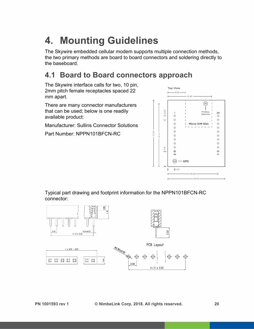
4. Mounting Guidelines The Skywire embedded cellular modem supports multiple connection methods, the two primary methods are board to board connectors and soldering directly to the baseboard.
4.1 Board to Board connectors approach The Skywire interface calls for two, 10 pin, 2mm pitch female receptacles spaced 22 mm apart. There are many connector manufacturers that can be used; below is one readily available product: Manufacturer: Sullins Connector Solutions Part Number: NPPN101BFCN-RC
Typical part drawing and footprint information for the NPPN101BFCN-RC connector:
PN 1001593 rev 1 © NimbeLink Corp. 2018. All rights reserved. 20

4.1.1 Mechanical Retention Certain applications where the modem is mounted on the host board using the connector approach detailed in section 4.1 may need to mechanically secure the Skywire modem & its SIM card in order to prevent the modem from vibrating out of the PCB. The Skywire modem does not have any dedicating attachment points for securing it to the host board, however it can easily be secured by one of the following methods:
● Zip tie ● Foam tape mounted on the Skywire to press against the housing ● Mechanical retention of the modem & SIM by the enclosure(example) ● Solder the Skywire to the host board (as described in section 4.2)
4.2 Solder to Board Connection The module can be soldered directly to a PCB. The PCB should be designed with two rows of ten, 0.8mm plated thru holes spaced 2mm apart. The two rows should be 22mm apart. See drawing below for recommended footprint. Measurements are in millimeters. U.FL locations are marked with circles, X1 on top side of board, X3 is on the bottom side of the board. J3 is Micro SIM card slot on bottom side of board. If the application is using GPS connector X3, the RF cable should be attached to the modem BEFORE the modem is soldered into the baseboard or else it may be difficult or impossible to attach the RF cable.
PN 1001593 rev 1 © NimbeLink Corp. 2018. All rights reserved. 21
5. Regulatory information 5.1 Carrier Specific Certifications NL-SW-LTE-TM1G-V: Verizon ODI (in progress) NL-SW-LTE-TM1G-A: PTCRB (in progress), AT&T (in progress)
5.2 Export Control Classification Number (ECCN) ECCNs are five character alpha-numeric designations used on the Commerce Control List (CCL) to identify dual-use items for export control purposes. An ECCN categorizes items based on the nature of the product, i.e. type of commodity, software, or technology and its respective technical parameters. ECCN for All Skywire Modems: 5A992.c
5.3 Harmonized Tariff Schedule Code HTS Code: 8517.62.0010
5.4 RoHS Compliance The NL-SW-LTE-TM1G modem family complies with the RoHS (Restriction of Hazardous Substances) directive of the European Union, EU Directive 2011/65/EU.
5.5 Interference statement This device complies with Part 15 of the FCC Rules and Industry Canada licence-exempt RSS standards. Operation is subject to the following two conditions: (1) This device may not cause harmful interferences, and (2) this device must accept any interference received, including interference that may cause undesired operation.
5.6 FCC & IC Compliance If the modem’s antenna is located farther than 20cm from the human body and there are no co-located transmitter then the modems underlying Telit modules FCC/IC approvals can be re-used by the end product. Should the modems antenna be mounted closer than 20cm from the human body or if there is are co-located transmitters then the additional FCC/IC testing may be required for the end product. The NL-SW-LTE-TM1G modems make use of the underlying Telit ME910C1 modules FCC & IC identification numbers.
PN 1001593 rev 1 © NimbeLink Corp. 2018. All rights reserved. 22
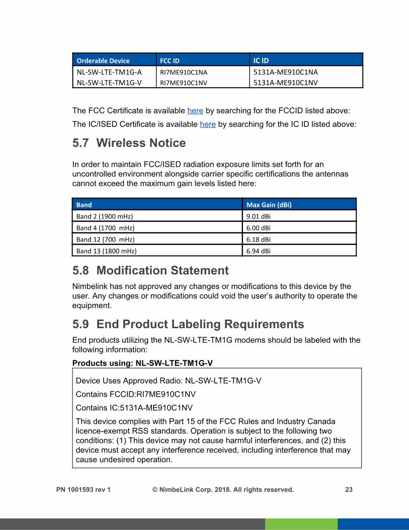
Orderable Device FCC ID IC ID
NL-SW-LTE-TM1G-A RI7ME910C1NA 5131A-ME910C1NA
NL-SW-LTE-TM1G-V RI7ME910C1NV 5131A-ME910C1NV
The FCC Certificate is available here by searching for the FCCID listed above: The IC/ISED Certificate is available here by searching for the IC ID listed above:
5.7 Wireless Notice In order to maintain FCC/ISED radiation exposure limits set forth for an uncontrolled environment alongside carrier specific certifications the antennas cannot exceed the maximum gain levels listed here:
Band Max Gain (dBi)
Band 2 (1900 mHz) 9.01 dBi
Band 4 (1700 mHz) 6.00 dBi
Band 12 (700 mHz) 6.18 dBi
Band 13 (1800 mHz) 6.94 dBi
5.8 Modification Statement Nimbelink has not approved any changes or modifications to this device by the user. Any changes or modifications could void the user’s authority to operate the equipment.
5.9 End Product Labeling Requirements End products utilizing the NL-SW-LTE-TM1G modems should be labeled with the following information: Products using: NL-SW-LTE-TM1G-V
Device Uses Approved Radio: NL-SW-LTE-TM1G-V Contains FCCID:RI7ME910C1NV Contains IC:5131A-ME910C1NV This device complies with Part 15 of the FCC Rules and Industry Canada licence-exempt RSS standards. Operation is subject to the following two conditions: (1) This device may not cause harmful interferences, and (2) this device must accept any interference received, including interference that may cause undesired operation.
PN 1001593 rev 1 © NimbeLink Corp. 2018. All rights reserved. 23

Products using: NL-SW-LTE-TM1G-A
Device Uses Approved Radio: NL-SW-LTE-TM1G-A FCCID:RI7ME910C1NA IC:5131A-ME910C1NA This device complies with Part 15 of the FCC Rules and Industry Canada licence-exempt RSS standards. Operation is subject to the following two conditions: (1) This device may not cause harmful interferences, and (2) this device must accept any interference received, including interference that may cause undesired operation.
PN 1001593 rev 1 © NimbeLink Corp. 2018. All rights reserved. 24