slwa063 | ti.com - semiconductor company | ti.com
TRANSCRIPT

Application NoteSLWA063–February 2011
Sideband Rejection and Feedback Isolation Impacts onDPD Performance
Nam, Kyung-wan................................................................................................ Wireless Infrastructure
ABSTRACT
Texas Instruments has DPD (Digital Pre-Distortion) chipsets for BTS (Basestation Transceiver System)and Repeater applications to improve overall system efficiency and meet various standard specifications.The GC5330 is an ultra-wideband transmit and receive signal processor that includes digital up/down-converters. The transmit path includes Crest Factor Reduction (CFR), Digital Pre-Distortion (DPD) andassociated feedback path, complex equalization, bulk up-conversion, complex equalization, and I/Qimbalance correction. This document describes what levels of sideband image rejection and feedbackpath isolation are required to achieve optimum DPD performance in Complex-IF Transmitter and Real-IFFeedback architecture.
Contents1 Introduction .................................................................................................................. 22 DPD Performance versus Sideband Image Level ...................................................................... 3
2.1 Test Setup Environment .......................................................................................... 32.2 Quadrature Modulation Correction for Different Level of the Sideband Image ............................ 42.3 Test Results ........................................................................................................ 52.4 Summary .......................................................................................................... 13
3 DPD Performance versus Isolation of Feedback Path with Adjacent Leakage Level ............................ 143.1 Test Setup Environment ......................................................................................... 143.2 Test Results ....................................................................................................... 153.3 Summary .......................................................................................................... 19
4 DPD Performance versus Isolation of Feedback Switch with Correlated Leakage Level ........................ 204.1 Test Setup Environment ......................................................................................... 204.2 Test Results ....................................................................................................... 214.3 Summary .......................................................................................................... 29
5 Summary ................................................................................................................... 30
1SLWA063–February 2011 Sideband Rejection and Feedback Isolation Impacts on DPD PerformanceSubmit Documentation Feedback
© 2011, Texas Instruments Incorporated

Introduction www.ti.com
1 Introduction
In a Quadrature system, the amplitude and phase imbalance between In-phase (I) and Quadrature-phase(Q) paths in the analog domain generate a sideband image component over the transmitted signal.Complex IF is chosen as a transmit arthitecture of GC5330SEK, which a complex IQ baseband signal isdirectly upconverted to Intermediate Frequency (IF) using coarse mixer block of DAC. This coarse mixingis simply done by complex-multiplying the mixing functions of 1/0/-1/0 for the cosine waveform and0/1/0/-1 for the sine waveform to the baseband I and Q rail respectively. Hence, sideband image ismirrored from local leakage and its diatance from carrier is twice of IF. Without appropriate filtering of thesideband on the transmission path, this image is fed into the input stage of the Power Amplifier (PA).Thus, the PA modeling is insufficiently accurate to adapt the transmitting signal well, as long as thesideband image is within the DPD processing bandwidth. Also, image interference aliased into the desiredfrequency band degrades the receiver performance.
Assuming inadequate feedback isolation, DPD performance is critical in the transceiver system becausethe feedback signal from the PA holds the leakage components in-band or very close to the in-bandsignal. This has a direct negative impact on the precise PA-model characterization, and eventuallydegrades the DPD correction performance.
Regarding feedback isolation test, the same LTE 1x10 MHz as main upper carrier is used as a leakagesignal to feedback path and the location of carrier leakage is adjacent to the main carrier. The centerfrequency of feedback signal, 2x10 MHz of LTE, to GC5330SEK is 2.14 GHz and the leakage signal, 1x10MHz of LTE, is located on 2.155 GHz as shown in Figure 35. Meanwhile, the same LTE 2x10 MHz asmain carriers is used as correlated leakage signals to feedback path and the location of correlatedleakage signal is the same as main carrier as 2.14 GHz as shown in Figure 49.
The quadrature modulation correction (QMC) block of the digital-to-analog converter (DAC) was used foreach different level of sideband image by manually tuning gain and phase. A power combiner with anexternal signal generator was used to generate the leakage signal input to feedback path in DPDarchitecture. The details of the test setup environments are addressed in Section 2.2, Section 3.1.1, andSection 4.1.1.
2 Sideband Rejection and Feedback Isolation Impacts on DPD Performance SLWA063–February 2011Submit Documentation Feedback
© 2011, Texas Instruments Incorporated

www.ti.com DPD Performance versus Sideband Image Level
2 DPD Performance versus Sideband Image Level
2.1 Test Setup Environment
The DPD performances were measured at 25, 30, and 35 dBm of Pout, depending on the various sidebandimage levels. The specifications of the setup are:• Test signal and its peak-to-average ratio (PAR): LTE FDD 2 x 10 MHz, 6.7 dB at 0.01%• Target board: TSW3100/GC5330SEK• RF center: 2140 MHz• IF: 153.6 MHz• LO: 1861.4 MHz• ADC sampling frequency: 204.8 MHz• DAC sampling frequency: 614.4 MHz after x4 interpolation in DAC• DPD BW: 153.6 MHz
Figure 1. CCDF Curve for Sideband Image versus DPD Performance
3SLWA063–February 2011 Sideband Rejection and Feedback Isolation Impacts on DPD PerformanceSubmit Documentation Feedback
© 2011, Texas Instruments Incorporated

SLWA063-002
Crossover cables
Router PC
PredriverBLF6G22-45
15 V
PredriverZHL-1724
Gain = 39 dB
15 V (Vg)28 V (Vds)15 V
Fan
Gain = 18.5 dB10.47 V
CPL
10.47 V
CPL
Fan
–20 dBBulk
–20 dBVAT –20
Power meter
Total Offset45.5 dB
SplitterMXA
2015 MHz
CMOSSync out
J55GC5330SEK
J39
FB In
J46
737.28 MHz/6 dBm(External VCXO)
ESG
TSW3100
SLWA063-059
DPD Performance versus Sideband Image Level www.ti.com
Figure 2. Test Setup for Sideband Image versus DPD Performance
2.2 Quadrature Modulation Correction for Different Level of the Sideband Image
The GC5330SEK includes the DAC3283 which is a dual-channel 16-bit, 800-Msps DAC. The QMC blockprovides a means for adjusting the gain and phase of the complex signal. At a quadrature modulatoroutput, gain and phase imbalances result in an undesired sideband signal.
The QMC block contains three programmable parameters: Offset, Gain A, and Gain B. Offset controls thephase imbalance between I and Q with 10-bit resolution and covers the range from –3.75 to +3.75degrees in 1024 steps. Gain A and Gain B consist of 11-bit resolution and control the gain of the I and Qpaths. By manually adjusting Offset, Gain A, or Gain B, the sideband image level can be controlled andreduced to the desired level.
Figure 3. QMC Window from GC5330 GUI
4 Sideband Rejection and Feedback Isolation Impacts on DPD Performance SLWA063–February 2011Submit Documentation Feedback
© 2011, Texas Instruments Incorporated

www.ti.com DPD Performance versus Sideband Image Level
2.3 Test Results
2.3.1 35 dBm of PA Output Power
The average output power of the BLF6G22-45 is 2.5 W (34 dBm) with 7.5 dB of PAR at 0.01%. For thistest, the test signal has 6.7 dB of PAR at 0.01% and therefore the output power of the PA is set to 35dBm.
Other parameters of the BLF6G22-45 are:• Frequency range: 2110–2170 MHz• VDS: 28 V• Gain: 18.5 dB• Efficiency (D): 13%• ACPR: –49 dBc (Test signal: 3GPP 64 DPCH with 7.5 dB of PAR at 0.01%, carrier spacing 5 MHz)
2.3.1.1 DPD Performance with –55 dBc of Sideband Image
Figure 4. –55 dBc of Image Level at 35 dBm of Pout Figure 5. Pre/Post DPD with –55 dBc of Image at35 dBm of Pout
Before enabling DPD, the sideband image is suppressed down to the noise floor by adjusting the QMC ofthe DAC, which is approximately –55 dBc from the main signal. This level does not impact DPDperformance.
5SLWA063–February 2011 Sideband Rejection and Feedback Isolation Impacts on DPD PerformanceSubmit Documentation Feedback
© 2011, Texas Instruments Incorporated

DPD Performance versus Sideband Image Level www.ti.com
2.3.1.2 DPD Performance with –45 dBc of Sideband Image
Figure 6. –45 dBc of Image Level at 35 dBm of Pout Figure 7. Pre/Post DPD with –45 dBc of Image at35 dBm of Pout
Figure 6 describes the level of sideband image at 800 MHz of span from the spectrum analyzer. Toillustrate the impact of different sideband levels on DPD performance, the pre/post DPD was kept for anexact comparison of the DPD performance.
The sideband image is adjusted to –45 dBc, as shown in Figure 6. The DPD performance with this level ofimage is the same as the DPD performance with –55 dBc of sideband level, as shown in Figure 7.
2.3.1.3 DPD Performance with –40 dBc of Sideband Image
Figure 8. –40 dBc of Image Level at 35 dBm of Pout Figure 9. Pre/Post DPD with –40 dBc of Image at35 dBm of Pout
The sideband image is adjusted to –40 dBc, as shown in Figure 8 . DPD performance with this level ofimage is the same as DPD performance with –55 dBc of the sideband level, as shown in Figure 9.
6 Sideband Rejection and Feedback Isolation Impacts on DPD Performance SLWA063–February 2011Submit Documentation Feedback
© 2011, Texas Instruments Incorporated

www.ti.com DPD Performance versus Sideband Image Level
2.3.1.4 DPD Performance with –39 dBc of Sideband Image
Figure 10. –39 dBc of Image Level at 35 dBm of Pout Figure 11. Pre/Post DPD with –39 dBc of Image at35 dBm of Pout
The sideband image is adjusted to –39 dBc, as shown in Figure 10. This level of sideband image starts toslightly degrade DPD performance, shown in Figure 11.
2.3.1.5 DPD Performance with –38 dBc of Sideband Image
Figure 12. –38 dBc of Image Level at 35 dBm of Pout Figure 13. Pre/Post DPD with –38 dBc of Image at35 dBm of Pout
The sideband image is adjusted to –38 dBc, as shown in Figure 12. This level of sideband imagedegrades DPD performance by 1–2 dB as compared to DPD performance with –55 dBc of sideband level,shown in Figure 13.
7SLWA063–February 2011 Sideband Rejection and Feedback Isolation Impacts on DPD PerformanceSubmit Documentation Feedback
© 2011, Texas Instruments Incorporated

DPD Performance versus Sideband Image Level www.ti.com
2.3.1.6 DPD Performance with –37 dBc of Sideband Image
Figure 14. –37 dBc of Image Level at 35 dBm of Pout Figure 15. Pre/Post DPD with –37 dBc of Image at35 dBm of Pout
The sideband image is adjusted to –37 dBc, as shown in Figure 14. The level of sideband imagedegrades DPD performance by 1–2 dB as compared to DPD performance of –55 dBc of sideband level,as shown in Figure 15.
2.3.1.7 DPD Performance with –36 dBc of Sideband Image
Figure 16. –36 dBc of Image Level at 35 dBm of Pout Figure 17. Pre/Post DPD with –36 dBc of Image at35 dBm of Pout
The sideband image is adjusted to –36 dBc, as shown in Figure 16. This level of sideband imagedegrades DPD performance by 1–2 dB as compared to DPD performance of –55 dBc of sideband level,as shown in Figure 17.
8 Sideband Rejection and Feedback Isolation Impacts on DPD Performance SLWA063–February 2011Submit Documentation Feedback
© 2011, Texas Instruments Incorporated

www.ti.com DPD Performance versus Sideband Image Level
2.3.1.8 DPD Performance with –35 dBc of Sideband Image
Figure 18. –35 dBc of Image Level at 35 dBm of Pout Figure 19. Pre/Post DPD with –35 dBc of Image at35 dBm of Pout
The sideband image is adjusted to –35 dBc, as shown in Figure 18. This level of sideband imagedegrades DPD performance by 1–2 dB, as compared to to DPD performance of –55 dBc of sidebandlevel, as shown in Figure 19.
2.3.1.9 DPD Performance with –30 dBc of Sideband Image
Figure 20. –30 dBc of Image Level at 35 dBm of Pout Figure 21. Pre/Post DPD with –30 dBc of Image at35 dBm of Pout
The sideband image is adjusted to –30 dBc, as shown in Figure 20. This level of sideband imagedegrades DPD performance by 2–3 dB as compared to DPD performance of –55 dBc of sideband level,as shown in Figure 21.
9SLWA063–February 2011 Sideband Rejection and Feedback Isolation Impacts on DPD PerformanceSubmit Documentation Feedback
© 2011, Texas Instruments Incorporated

DPD Performance versus Sideband Image Level www.ti.com
2.3.1.10 DPD Performance with –25 dBc of Sideband Image
Figure 22. –25 dBc of Image Level at 35 dBm of Pout Figure 23. Pre/Post DPD with –25 dBc of Image at35 dBm of Pout
The sideband image is adjusted to –25 dBc, as shown in Figure 22. This level of sideband imagedegrades DPD performance by 5–6 dB as compared to DPD performance of –55 dBc of sideband level,as shown in Figure 23.
10 Sideband Rejection and Feedback Isolation Impacts on DPD Performance SLWA063–February 2011Submit Documentation Feedback
© 2011, Texas Instruments Incorporated

www.ti.com DPD Performance versus Sideband Image Level
2.3.2 30 dBm of PA Output Power
The output power of the target PA was reduced by 5 dB of the maximum output power to check how muchsideband image impacts the DPD performance at lower levels.
2.3.2.1 DPD Performance with –50 dBc of Sideband Image
Figure 24. –50 dBc of Image Level at 30 dBm of Pout Figure 25. Pre/Post DPD Correction with –50 dBc ofImage at 30 dBm of Pout
The sideband image is adjusted to –50 dBc, as shown in Figure 24. DPD performance with this level ofsideband image does not degrade the DPD performance, as shown in Figure 25.
2.3.2.2 DPD Performance with –30 dBc of Sideband Image
Figure 26. –30 dBc of Image Level at 30 dBm of Pout Figure 27. Pre/Post DPD Correction with –30 dBc ofImage at 30 dBm of Pout
The sideband image is adjusted to –30 dBc, as shown in Figure 26. DPD performance with this level ofsideband image does not degrade the DPD performance, as shown in Figure 27.
11SLWA063–February 2011 Sideband Rejection and Feedback Isolation Impacts on DPD PerformanceSubmit Documentation Feedback
© 2011, Texas Instruments Incorporated

DPD Performance versus Sideband Image Level www.ti.com
2.3.2.3 DPD Performance with –25 dBc of Sideband Image
Figure 28. –25 dBc of Image Level at 30 dBm of Pout Figure 29. Pre/Post DPD Correction with –25 dBc ofImage at 30 dBm of Pout
The sideband image is adjusted to –25 dBc, as shown in Figure 28. DPD performance with this level ofsideband image does not degrade the DPD performance, as shown in Figure 29.
2.3.3 25 dBm of PA Output Power
The output power of the target PA was reduced by 10 dB from the maximum output power to check howmuch sideband image impacts the DPD performance at lower levels.
2.3.3.1 DPD Performance with –50 dBc of Sideband Image
Figure 30. –50 dBc of Image Level at 25 dBm of Pout Figure 31. Pre/Post DPD Correction with –50 dBc ofImage at 30 dBm of Pout
The sideband image is adjusted to –50 dBc, as shown in Figure 30. DPD performance with this level ofsideband image does not degrade the DPD performance at 25 dBm of PA output power, as shown inFigure 31.
12 Sideband Rejection and Feedback Isolation Impacts on DPD Performance SLWA063–February 2011Submit Documentation Feedback
© 2011, Texas Instruments Incorporated

www.ti.com DPD Performance versus Sideband Image Level
2.3.3.2 DPD Performance with –25 dBc of Sideband Image
Figure 32. –25 dBc of Image Level at 30 dBm of Pout Figure 33. Pre/Post DPD Correction with –25 dBc ofImage at 30 dBm of Pout
The sideband image is adjusted to –25 dBc, as shown in Figure 32. DPD performance with this level ofsideband image does not degrade the DPD performance at 25 dBm of PA output power, as shown inFigure 33, even though the sideband image level is –25 dBc to the carrier.
2.4 Summary
DPD performance starts degrading at –39 dBc of sideband image level at the maximum output power ofthe PA from this test. This means at least –40 dBc of sideband-image rejection is required to avoiddegradation of DPD performance. At 5 and 10 dB of reduction from the maximum PA output power, 30and 25 dBm, respectively, the sideband image does not degrade DPD performance at all.
Table 1. Sideband Image Level versus DPD Performance
Sideband Image Level –25 dBc –30 dBc –35 dBc –39 dBc –40 dBc –45 dBc
DPD performance (1) (2) (3) X X Δ Δ O O(1) X: More than 2–3 dB degraded DPD performance from sideband image(2) Δ: Less than 1–2 dB degraded DPD performance from sideband image(3) O: No degradation from the standard DPD performance
13SLWA063–February 2011 Sideband Rejection and Feedback Isolation Impacts on DPD PerformanceSubmit Documentation Feedback
© 2011, Texas Instruments Incorporated

DPD Performance versus Isolation of Feedback Path with Adjacent Leakage Level www.ti.com
3 DPD Performance versus Isolation of Feedback Path with Adjacent Leakage Level
3.1 Test Setup Environment
DPD performances were measured at 36 dBm of maximum Pout depending on adjacent leakage levelthrough the feedback switch from other channels. The specifications of setup are:
• Test signal and its PAR: LTE FDD 2 x 10 MHz, 6.7 dB at 0.01%• Target board: TSW3100/GC5330SEK• RF center: 2140 MHz• IF: 153.6 MHz• LO: 1861.4 MHz• ADC sampling frequency: 204.8 MHz• DAC sampling frequency: 614.4 MHz after x4 interpolation in DAC• DPD BW: 153.6 MHz• FB input: 3 dBm• Pout: 36 dBm (The maximum Pout of BLFG6G22 is 34 dBm with 7.5 dB of PAR at 0.01%.) → 1 dB
higher than specified Pout
Figure 34. CCDF Curve for DPD Performance versus Adjacent Leakage of Feedback Switch
14 Sideband Rejection and Feedback Isolation Impacts on DPD Performance SLWA063–February 2011Submit Documentation Feedback
© 2011, Texas Instruments Incorporated

SLWA063-034
Crossover cables
Router PC
PABLF6G22-45
PredriverZHL-3500
Gain = 21 dB
15 V (Vg)28 V (Vds)12 V
Fan
Gain = 18.5 dB10.47 V
CPL
CPL
–20 dBBulk
–20 dBVAT –20
Power meter
PSA
2.14 MHz
GC5330SEK
J39
FB In
LTE 2 x 10 MHZ @ 2.14 GHz
E4438C
TSW3100
Power divider
LTE 10 MHZ @ 2.155 GHz
36 dBm
www.ti.com DPD Performance versus Isolation of Feedback Path with Adjacent Leakage Level
Figure 35. Test Setup for DPD Performance versus Adjacent Leakage of Feedback Switch
3.1.1 Adjacent Leakage Level
The adjacent carrier baseband signal can be downloaded to the E4438C and the level of adjacent leakagelevel can be controlled by adjusting the level of the amplitude from the signal generator.
3.2 Test Results
3.2.1 DPD Performance without Adjacent Leakage
Figure 36. No Adjacent Leakage Into Feedback Figure 37. Pre/Post DPD Correction without Leakage
15SLWA063–February 2011 Sideband Rejection and Feedback Isolation Impacts on DPD PerformanceSubmit Documentation Feedback
© 2011, Texas Instruments Incorporated

DPD Performance versus Isolation of Feedback Path with Adjacent Leakage Level www.ti.com
3.2.2 DPD Performance with –20 dBc of Adjacent Leakage Level
Figure 38. –20 dBc of Adjacent Leakage Into Feedback Figure 39. Pre/Post DPD Correction with –20 dBc ofLeakage
The DPD performance is severely degraded by –20 dBc of adjacent leakage from the feedback path, asshown in Figure 38. More than 10 dB of correction is degraded by bad feedback isolation, as shown inFigure 39.
3.2.3 DPD Performance with –30 dBc of Adjacent Leakage Level
Figure 40. –30 dBc of Adjacent Leakage Into Feedback Figure 41. Pre/Post DPD Correction with –30 dBc ofLeakage
The DPD performance is degraded by –30 dBc of adjacent leakage from the feedback path, as shown inFigure 40. Several dB of correction is degraded by bad feedback isolation, as shown in Figure 41.
16 Sideband Rejection and Feedback Isolation Impacts on DPD Performance SLWA063–February 2011Submit Documentation Feedback
© 2011, Texas Instruments Incorporated

www.ti.com DPD Performance versus Isolation of Feedback Path with Adjacent Leakage Level
3.2.4 DPD Performance with –40 dBc of Adjacent Leakage Level
Figure 42. –40 dBc of Adjacent Leakage Into Feedback Figure 43. Pre/Post DPD Correction with –40 dBc ofLeakage
The DPD performance is degraded by –40 dBc of adjacent leakage from the feedback path, as shown inFigure 42. A small amount of correction is degraded by bad feedback isolation, as shown in Figure 43.Some fluctuation is observed at this level.
3.2.5 DPD Performance with –45 dBc of Adjacent Leakage Level
Figure 44. –45 dBc of Adjacent Leakage Into Feedback Figure 45. Pre/Post DPD Correction with –45 dBc ofLeakage
The DPD performance is the same as nonadjacent leakage from the feedback switch.
17SLWA063–February 2011 Sideband Rejection and Feedback Isolation Impacts on DPD PerformanceSubmit Documentation Feedback
© 2011, Texas Instruments Incorporated

DPD Performance versus Isolation of Feedback Path with Adjacent Leakage Level www.ti.com
3.2.6 DPD Performance with –50 dBc of Adjacent Leakage Level
Figure 46. –50 dBc of Adjacent Leakage Into Feedback Figure 47. Pre/Post DPD Correction with –50 dBc ofLeakage
The DPD performance is the same as nonadjacent leakage from the feedback switch.
18 Sideband Rejection and Feedback Isolation Impacts on DPD Performance SLWA063–February 2011Submit Documentation Feedback
© 2011, Texas Instruments Incorporated

www.ti.com DPD Performance versus Isolation of Feedback Path with Adjacent Leakage Level
3.3 Summary
DPD performance starts degrading at –40 dBc of adjacent leakage carrier from the feedback switch at themaximum output power of the PA. A small amount of fluctuation is observed at the location of adjacentleakage during adaptation. A minimum of –45 dBc of feedback isolation is required to avoid degradation ofthe DPD performance. For this test, BPF (Fc = 2.14 GHz with 150 MHz of BW) is used to exclude theimpact of the sideband image and DC offset over DPD performance.
Table 2. Adjacent Leakge Level versus DPD Performance
Adjacent Leakage Level –20 dBc –30 dBc –40 dBc –45 dBc
DPD performance (1) (2) (3) X X Δ O(1) X: More than 2–3 dB degraded DPD performance from adjacent leakage(2) Δ: Less than 1–2 dB degraded DPD performance from adjacent leakage(3) O: No degradation from the standard DPD performance
19SLWA063–February 2011 Sideband Rejection and Feedback Isolation Impacts on DPD PerformanceSubmit Documentation Feedback
© 2011, Texas Instruments Incorporated
DPD Performance versus Isolation of Feedback Switch with Correlated Leakage Level www.ti.com
4 DPD Performance versus Isolation of Feedback Switch with Correlated LeakageLevel
4.1 Test Setup Environment
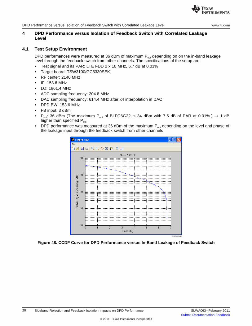
DPD performances were measured at 36 dBm of maximum Pout depending on on the in-band leakagelevel through the feedback switch from other channels. The specifications of the setup are:• Test signal and its PAR: LTE FDD 2 x 10 MHz, 6.7 dB at 0.01%• Target board: TSW3100/GC5330SEK• RF center: 2140 MHz• IF: 153.6 MHz• LO: 1861.4 MHz• ADC sampling frequency: 204.8 MHz• DAC sampling frequency: 614.4 MHz after x4 interpolation in DAC• DPD BW: 153.6 MHz• FB input: 3 dBm• Pout: 36 dBm (The maximum Pout of BLFG6G22 is 34 dBm with 7.5 dB of PAR at 0.01%.) → 1 dB
higher than specified Pout
• DPD performance was measured at 36 dBm of the maximum Pout depending on the level and phase ofthe leakage input through the feedback switch from other channels
Figure 48. CCDF Curve for DPD Performance versus In-Band Leakage of Feedback Switch
20 Sideband Rejection and Feedback Isolation Impacts on DPD Performance SLWA063–February 2011Submit Documentation Feedback
© 2011, Texas Instruments Incorporated

SLWA063-048
Crossover cables
Router PC
PABLF6G22-45
PredriverZRL-3500
Gain = 21 dB
15 V (Vg)28 V (Vds)12 V
Fan
Gain = 18.5 dB10.47 V
CPL
CPL
–20 dBBulk
–20 dBVAT –20
Power meter
PSA
GC5330SEK
J39
FB In
LTE 2 x 10 MHZ@ 2.14 GHz
TSW3100
Power divider
36 dBm
TXC
TXD
LTE 2 x 10 MHZ@ 2.14 GHz
LTE 2 x 10 MHZ @ 2.14 GHz
www.ti.com DPD Performance versus Isolation of Feedback Switch with Correlated Leakage Level
Figure 49. Test Setup for DPD Performance versus In-Band Leakage of Feedback Switch
4.1.1 In-Band Leakage Level
In-band leakage is generated from another channel of GC5330SEK called TXD. The in-band leakagesignal can be the same signal of the transmit channel as TXC and its level can be controlled by adjustingan on-board attenuator through the GC5330 GUI. This in-band leakage signal is fed into a power dividerand is merged with the feedback signal at the same frequency.
4.2 Test Results
4.2.1 DPD Performance without Leakage and Phase Offset
Figure 50. No In-Band Leakage From Feedback Figure 51. Pre/Post DPD Correction without In-BandLeakage
To avoid the impact of the sideband image for in-band leakage testing, the sideband image was correcteddown to the noise floor, as shown in Figure 50. Figure 51 shows the pre/post DPD without in-bandleakage.
21SLWA063–February 2011 Sideband Rejection and Feedback Isolation Impacts on DPD PerformanceSubmit Documentation Feedback
© 2011, Texas Instruments Incorporated

DPD Performance versus Isolation of Feedback Switch with Correlated Leakage Level www.ti.com
4.2.2 No Phase Offset From In-Band Leakage
4.2.2.1 DPD Performance with –20 dBc of In-Band Leakage From Feedback Switch
Figure 52. DPD Performance with –20 dBc of In-Band Leakage
The DPD performance is degraded by several dB due to bad isolation of the feedback switch, but it isbetter compared to the adjacent leakage. The in-band leakage is hidden in the in-band carrier, so it cannot be observed.
22 Sideband Rejection and Feedback Isolation Impacts on DPD Performance SLWA063–February 2011Submit Documentation Feedback
© 2011, Texas Instruments Incorporated

www.ti.com DPD Performance versus Isolation of Feedback Switch with Correlated Leakage Level
4.2.2.2 DPD Performance with –30 dBc of Feedback Leakage
Figure 53. DPD Performance with –30 dBc of In-Band Leakage
The DPD performance is degraded by a couple of dB due to bad isolation of the feedback switch. But it isbetter compared to the adjacent leakage.
23SLWA063–February 2011 Sideband Rejection and Feedback Isolation Impacts on DPD PerformanceSubmit Documentation Feedback
© 2011, Texas Instruments Incorporated

DPD Performance versus Isolation of Feedback Switch with Correlated Leakage Level www.ti.com
4.2.2.3 DPD Performance with –40 dBc of Feedback Leakage
Figure 54. DPD Performance with –40 dBc of In-Band Leakage
The DPD performance shows a small amount of degradation at –40 dBc of in-band leakage compared tothe performance without in-band leakage.
24 Sideband Rejection and Feedback Isolation Impacts on DPD Performance SLWA063–February 2011Submit Documentation Feedback
© 2011, Texas Instruments Incorporated
www.ti.com DPD Performance versus Isolation of Feedback Switch with Correlated Leakage Level
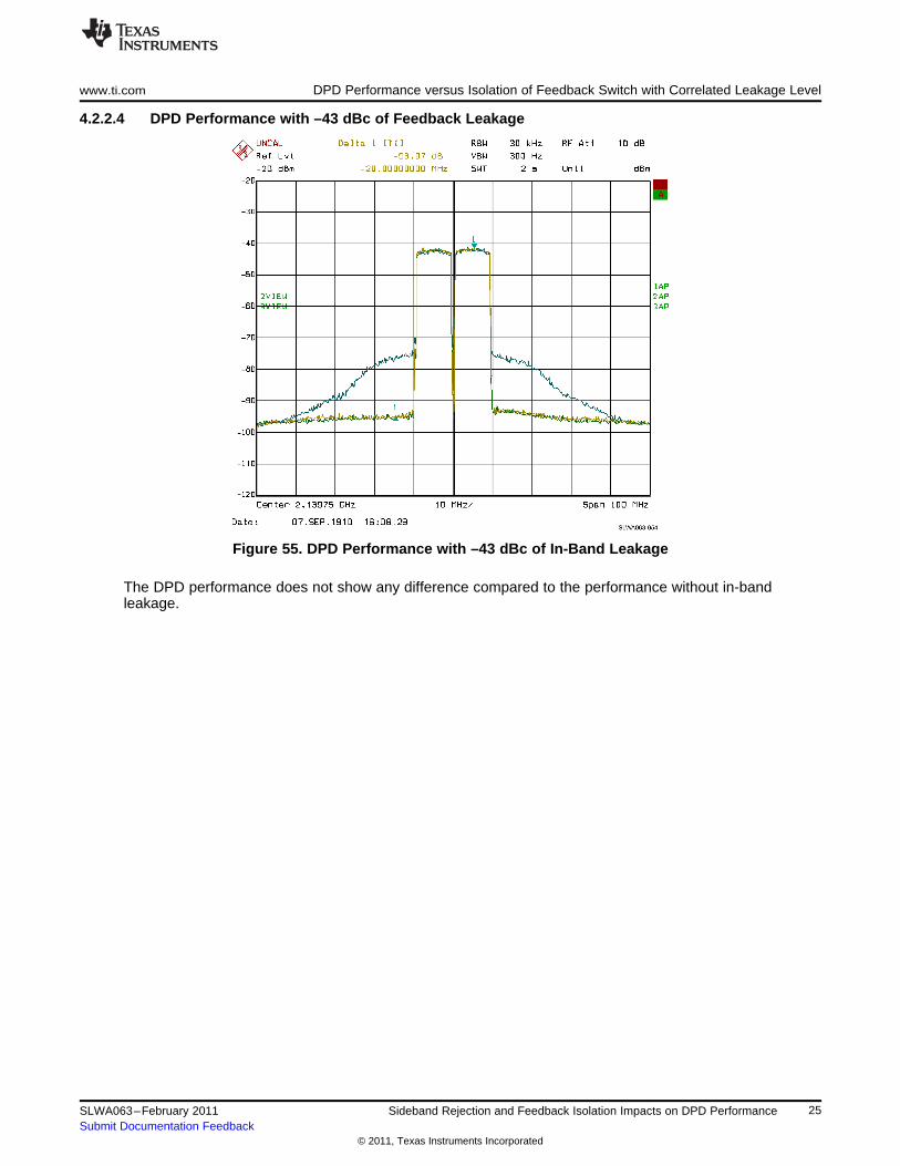
4.2.2.4 DPD Performance with –43 dBc of Feedback Leakage
Figure 55. DPD Performance with –43 dBc of In-Band Leakage
The DPD performance does not show any difference compared to the performance without in-bandleakage.
25SLWA063–February 2011 Sideband Rejection and Feedback Isolation Impacts on DPD PerformanceSubmit Documentation Feedback
© 2011, Texas Instruments Incorporated
DPD Performance versus Isolation of Feedback Switch with Correlated Leakage Level www.ti.com
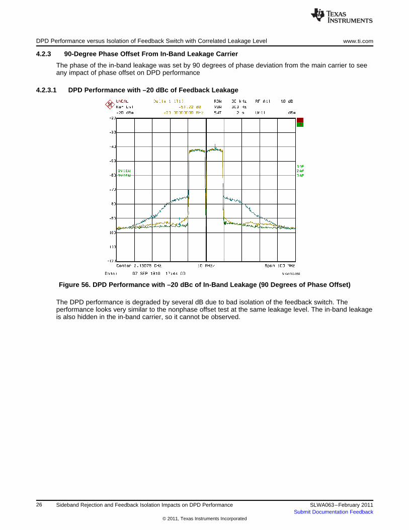
4.2.3 90-Degree Phase Offset From In-Band Leakage Carrier
The phase of the in-band leakage was set by 90 degrees of phase deviation from the main carrier to seeany impact of phase offset on DPD performance
4.2.3.1 DPD Performance with –20 dBc of Feedback Leakage
Figure 56. DPD Performance with –20 dBc of In-Band Leakage (90 Degrees of Phase Offset)
The DPD performance is degraded by several dB due to bad isolation of the feedback switch. Theperformance looks very similar to the nonphase offset test at the same leakage level. The in-band leakageis also hidden in the in-band carrier, so it cannot be observed.
26 Sideband Rejection and Feedback Isolation Impacts on DPD Performance SLWA063–February 2011Submit Documentation Feedback
© 2011, Texas Instruments Incorporated

www.ti.com DPD Performance versus Isolation of Feedback Switch with Correlated Leakage Level
4.2.3.2 DPD Performance with –30 dBc of Feedback Leakage
Figure 57. DPD Performance with –30 dBc of In-Band Leakage (90 Degrees of Phase Offset)
The DPD performance is degraded by 1–2 dB due to bad isolation of the feedback switch. Theperformance looks very similar to the nonphase offset test at the same leakage level.
27SLWA063–February 2011 Sideband Rejection and Feedback Isolation Impacts on DPD PerformanceSubmit Documentation Feedback
© 2011, Texas Instruments Incorporated

DPD Performance versus Isolation of Feedback Switch with Correlated Leakage Level www.ti.com
4.2.3.3 DPD Performance with –40 dBc of Feedback Leakage
Figure 58. DPD Performance with –40 dBc of In-Band Leakage (90 Degrees of Phase Offset)
The DPD performance shows a small amount of degradation at –40 dBc of in-band leakage compared tothe performance without in-band leakage.
28 Sideband Rejection and Feedback Isolation Impacts on DPD Performance SLWA063–February 2011Submit Documentation Feedback
© 2011, Texas Instruments Incorporated
www.ti.com DPD Performance versus Isolation of Feedback Switch with Correlated Leakage Level
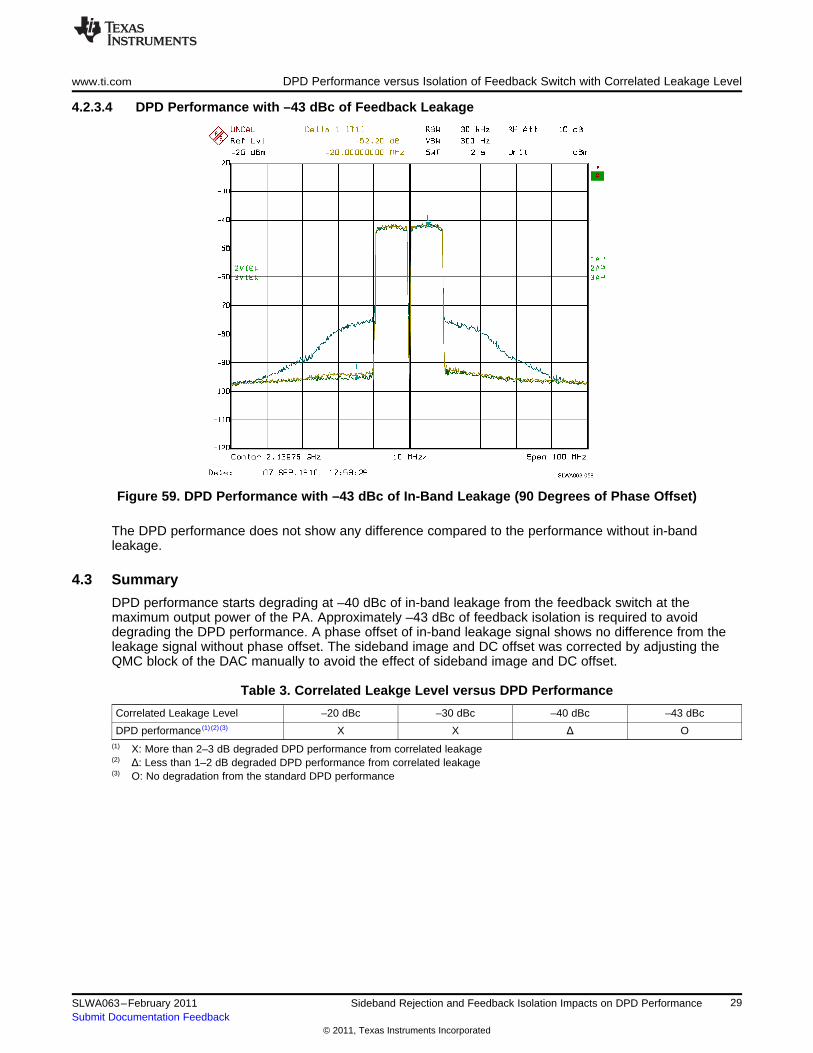
4.2.3.4 DPD Performance with –43 dBc of Feedback Leakage
Figure 59. DPD Performance with –43 dBc of In-Band Leakage (90 Degrees of Phase Offset)
The DPD performance does not show any difference compared to the performance without in-bandleakage.
4.3 Summary
DPD performance starts degrading at –40 dBc of in-band leakage from the feedback switch at themaximum output power of the PA. Approximately –43 dBc of feedback isolation is required to avoiddegrading the DPD performance. A phase offset of in-band leakage signal shows no difference from theleakage signal without phase offset. The sideband image and DC offset was corrected by adjusting theQMC block of the DAC manually to avoid the effect of sideband image and DC offset.
Table 3. Correlated Leakge Level versus DPD Performance
Correlated Leakage Level –20 dBc –30 dBc –40 dBc –43 dBc
DPD performance (1) (2) (3) X X Δ O(1) X: More than 2–3 dB degraded DPD performance from correlated leakage(2) Δ: Less than 1–2 dB degraded DPD performance from correlated leakage(3) O: No degradation from the standard DPD performance
29SLWA063–February 2011 Sideband Rejection and Feedback Isolation Impacts on DPD PerformanceSubmit Documentation Feedback
© 2011, Texas Instruments Incorporated

Summary www.ti.com
5 Summary
DPD performance shows difference under various test conditions such as sideband image level andadjacent and correlated leakage level into feedback path from GC5330SEK. Without a properly designedanalog filter, –40 dBc of sideband suppression from the main carrier should be achieved to get theoptimum result of DPD correction at the maximum output power of power amplifier. Otherwise, the DPDperformance starts degrading from –39 dBc by 1–2 dB of correction and gets worse as the sidebandimage level increases. Regarding adjacent and correlated leakage into feedback path, the isolationbetween the transmit and feedback paths should be at least –45 dBc and –43 dBc, respectively, to get theoptimum DPD performances. Otherwise, DPD performance degrades as leakage level increases.
Table 4. Sideband and Leakge Level versus DPD Performance
Sideband and Leakage –20 dBc –25 dBc –30 dBc –35 dBc –39 dBc –40 dBc –43 dBc –45 dBcLevel (1) (2) (3)
DPD performance vs Sideband X X X Δ Δ O O OImage
DPD performance vs Adjacent X X X X X Δ Δ OLeakage
DPD performance vs Correlated X X X X X Δ O OLeakage(1) X: More than 2–3 dB degraded DPD performance from correlated leakage(2) Δ: Less than 1–2 dB degraded DPD performance from correlated leakage(3) O: No degradation from the standard DPD performance
30 Sideband Rejection and Feedback Isolation Impacts on DPD Performance SLWA063–February 2011Submit Documentation Feedback
© 2011, Texas Instruments Incorporated

IMPORTANT NOTICE
Texas Instruments Incorporated and its subsidiaries (TI) reserve the right to make corrections, modifications, enhancements, improvements,and other changes to its products and services at any time and to discontinue any product or service without notice. Customers shouldobtain the latest relevant information before placing orders and should verify that such information is current and complete. All products aresold subject to TI’s terms and conditions of sale supplied at the time of order acknowledgment.
TI warrants performance of its hardware products to the specifications applicable at the time of sale in accordance with TI’s standardwarranty. Testing and other quality control techniques are used to the extent TI deems necessary to support this warranty. Except wheremandated by government requirements, testing of all parameters of each product is not necessarily performed.
TI assumes no liability for applications assistance or customer product design. Customers are responsible for their products andapplications using TI components. To minimize the risks associated with customer products and applications, customers should provideadequate design and operating safeguards.
TI does not warrant or represent that any license, either express or implied, is granted under any TI patent right, copyright, mask work right,or other TI intellectual property right relating to any combination, machine, or process in which TI products or services are used. Informationpublished by TI regarding third-party products or services does not constitute a license from TI to use such products or services or awarranty or endorsement thereof. Use of such information may require a license from a third party under the patents or other intellectualproperty of the third party, or a license from TI under the patents or other intellectual property of TI.
Reproduction of TI information in TI data books or data sheets is permissible only if reproduction is without alteration and is accompaniedby all associated warranties, conditions, limitations, and notices. Reproduction of this information with alteration is an unfair and deceptivebusiness practice. TI is not responsible or liable for such altered documentation. Information of third parties may be subject to additionalrestrictions.
Resale of TI products or services with statements different from or beyond the parameters stated by TI for that product or service voids allexpress and any implied warranties for the associated TI product or service and is an unfair and deceptive business practice. TI is notresponsible or liable for any such statements.
TI products are not authorized for use in safety-critical applications (such as life support) where a failure of the TI product would reasonablybe expected to cause severe personal injury or death, unless officers of the parties have executed an agreement specifically governingsuch use. Buyers represent that they have all necessary expertise in the safety and regulatory ramifications of their applications, andacknowledge and agree that they are solely responsible for all legal, regulatory and safety-related requirements concerning their productsand any use of TI products in such safety-critical applications, notwithstanding any applications-related information or support that may beprovided by TI. Further, Buyers must fully indemnify TI and its representatives against any damages arising out of the use of TI products insuch safety-critical applications.
TI products are neither designed nor intended for use in military/aerospace applications or environments unless the TI products arespecifically designated by TI as military-grade or "enhanced plastic." Only products designated by TI as military-grade meet militaryspecifications. Buyers acknowledge and agree that any such use of TI products which TI has not designated as military-grade is solely atthe Buyer's risk, and that they are solely responsible for compliance with all legal and regulatory requirements in connection with such use.
TI products are neither designed nor intended for use in automotive applications or environments unless the specific TI products aredesignated by TI as compliant with ISO/TS 16949 requirements. Buyers acknowledge and agree that, if they use any non-designatedproducts in automotive applications, TI will not be responsible for any failure to meet such requirements.
Following are URLs where you can obtain information on other Texas Instruments products and application solutions:
Products Applications
Audio www.ti.com/audio Communications and Telecom www.ti.com/communications
Amplifiers amplifier.ti.com Computers and Peripherals www.ti.com/computers
Data Converters dataconverter.ti.com Consumer Electronics www.ti.com/consumer-apps
DLP® Products www.dlp.com Energy and Lighting www.ti.com/energy
DSP dsp.ti.com Industrial www.ti.com/industrial
Clocks and Timers www.ti.com/clocks Medical www.ti.com/medical
Interface interface.ti.com Security www.ti.com/security
Logic logic.ti.com Space, Avionics and Defense www.ti.com/space-avionics-defense
Power Mgmt power.ti.com Transportation and www.ti.com/automotiveAutomotive
Microcontrollers microcontroller.ti.com Video and Imaging www.ti.com/video
RFID www.ti-rfid.com Wireless www.ti.com/wireless-apps
RF/IF and ZigBee® Solutions www.ti.com/lprf
TI E2E Community Home Page e2e.ti.com
Mailing Address: Texas Instruments, Post Office Box 655303, Dallas, Texas 75265Copyright © 2011, Texas Instruments Incorporated