s/m ctk-501 - warning will robinson ctk501 service man… · ctk-501 ctk-501 fill-in ... chord book...
TRANSCRIPT
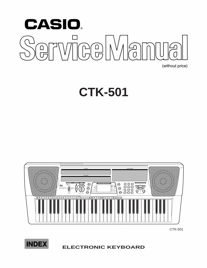
ELECTRONIC KEYBOARD
CTK-501
CTK-501
100 SONG BANNK100 TONES
100 RHYTHMS
POWER/MODE MAIN VOLUME TEMPOMUSICAL INFORMATION SYSTEM
TONERHYTHM
SONG BANKSTATUS
TEMPOMAIN VOLUME
FINGERING/PART
LEFT/ACCOMP
RIGHT/MELODY
:1 OCTAVE UP
:PEDAL(SUSTAIN)
100 SONG BANNK KEYBOARD
MUSICAL INFORMATION SYSTEMON
OFF
FINGERED
SYNCHRO/FILL-IN
CHORD BOOK TONE
M m
M7 dim aug
7
sus4 -5 add9
CLEAR 0
1 2 3
4 5 6
7 8 9
RHYTHM
STOP
REW
LEFT RIGHT
ON/OFF
PLAY/PAUSE
FF
SONG BANK
TRANSPOSE/TUNE/MIDI
ACCOMPVOLUME
START/STOP
CASIO CHORDNORMALSONG BANK CONTROLLER
SONG BANK CONTROLLER

CONTENTS
Specifications ................................................................................................................................... 1
Block Diagram .................................................................................................................................. 2
Circuit Description ............................................................................................................................ 3
Adjustment ....................................................................................................................................... 7
Major Waveforms ............................................................................................................................. 8
Printed Circuit Boards ...................................................................................................................... 9
Schematic Diagrams ...................................................................................................................... 11
Exploded View ............................................................................................................................... 16
Parts List ........................................................................................................................................ 17
— 1 —
ELECTRICALCurrent drain with 9 V DC:
No sound output 120 mA ± 20%Maximum volume 750 mA ± 20%
with 12 keys C1 to B1 pressed in Synth-Lead 1Volume: Maximum
Phone output level (Vrms with 8 Ω load each channel):with key G2 pressed in Synth-Lead 1 78 mV ± 20%
Speaker output level (Vrms with 4 Ω load each channel):with key G1 pressed in Synth-Lead 1 1250 mV ± 20%
Minimum operating voltage: 6.0 V
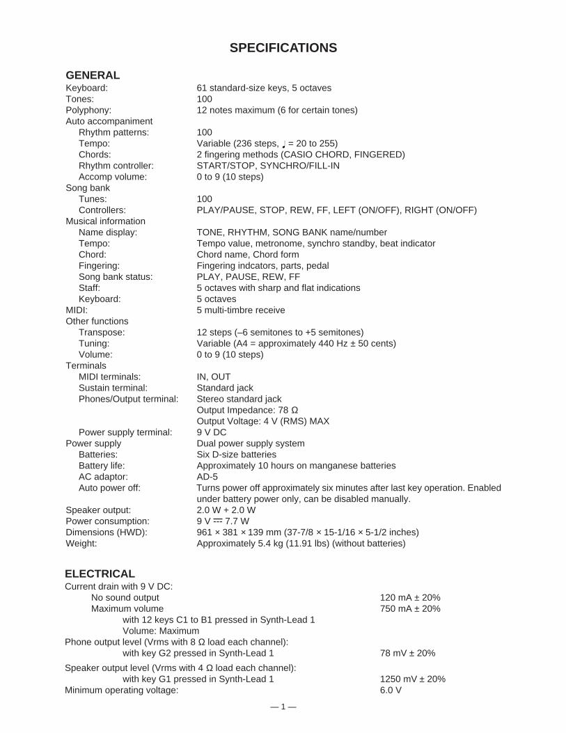
SPECIFICATIONS
GENERALKeyboard: 61 standard-size keys, 5 octavesTones: 100Polyphony: 12 notes maximum (6 for certain tones)Auto accompaniment
Rhythm patterns: 100Tempo: Variable (236 steps, = 20 to 255)Chords: 2 fingering methods (CASIO CHORD, FINGERED)Rhythm controller: START/STOP, SYNCHRO/FILL-INAccomp volume: 0 to 9 (10 steps)
Song bankTunes: 100Controllers: PLAY/PAUSE, STOP, REW, FF, LEFT (ON/OFF), RIGHT (ON/OFF)
Musical informationName display: TONE, RHYTHM, SONG BANK name/numberTempo: Tempo value, metronome, synchro standby, beat indicatorChord: Chord name, Chord formFingering: Fingering indcators, parts, pedalSong bank status: PLAY, PAUSE, REW, FFStaff: 5 octaves with sharp and flat indicationsKeyboard: 5 octaves
MIDI: 5 multi-timbre receiveOther functions
Transpose: 12 steps (–6 semitones to +5 semitones)Tuning: Variable (A4 = approximately 440 Hz ± 50 cents)Volume: 0 to 9 (10 steps)
TerminalsMIDI terminals: IN, OUTSustain terminal: Standard jackPhones/Output terminal: Stereo standard jack
Output Impedance: 78 ΩOutput Voltage: 4 V (RMS) MAX
Power supply terminal: 9 V DCPower supply Dual power supply system
Batteries: Six D-size batteriesBattery life: Approximately 10 hours on manganese batteriesAC adaptor: AD-5Auto power off: Turns power off approximately six minutes after last key operation. Enabled
under battery power only, can be disabled manually.Speaker output: 2.0 W + 2.0 WPower consumption: 9 V --- 7.7 WDimensions (HWD): 961 × 381 × 139 mm (37-7/8 × 15-1/16 × 5-1/2 inches)Weight: Approximately 5.4 kg (11.91 lbs) (without batteries)
— 2 —
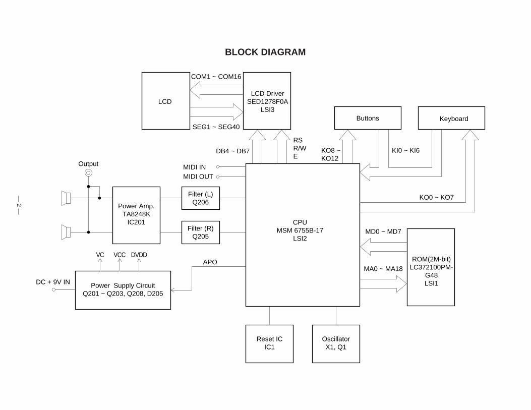
BLOCK DIAGRAM
CPUMSM 6755B-17
LSI2
KeyboardButtons
LCDLCD Driver
SED1278F0ALSI3
Reset ICIC1
OscillatorX1, Q1
Power Supply CircuitQ201 ~ Q203, Q208, D205
Power Amp.TA8248K
IC201
Filter (L)Q206
Filter (R)Q205
Output
VC VCC DVDDAPO
DC + 9V IN
DB4 ~ DB7
MIDI INMIDI OUT
COM1 ~ COM16
SEG1 ~ SEG40
RSR/WE
KO8 ~KO12
KI0 ~ KI6
KO0 ~ KO7
MD0 ~ MD7
MA0 ~ MA18ROM(2M-bit)
LC372100PM-G48LSI1
— 3 —
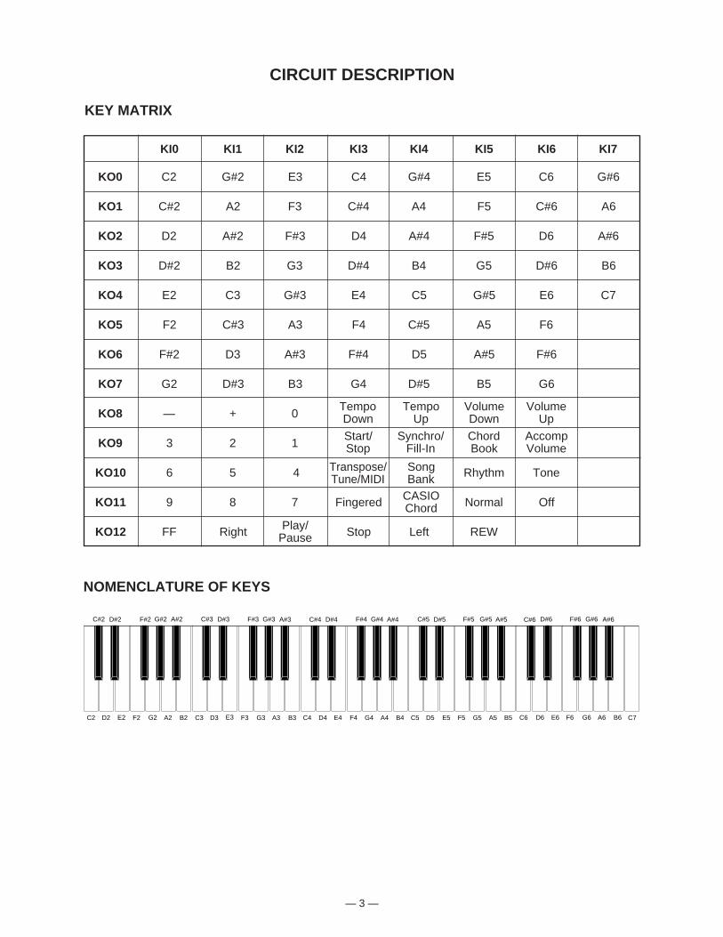
CIRCUIT DESCRIPTION
KEY MATRIX
F#3 G#3 A#3 C#4 D#4 F#4 G#4 A#4 C#5 D#5 F#5 G#5 A#5
F3 G3 A3 B3 C4 D4 E4 F4 G4 A4 B4 C5 D5 E5 F5 G5 A5 B5 C6
D#3
C2 D2 E2 F2 G2 A2 B2 C3 D3 E3 B6A6G6F6E6D6 C7
C#3A#2G#2F#2D#2C#2 A#6G#6F#6D#6C#6
NOMENCLATURE OF KEYS
KI0 KI1 KI2 KI3 KI4 KI5 KI6 KI7
KO0 C2 G#2 E3 C4 G#4 E5 C6 G#6
KO1 C#2 A2 F3 C#4 A4 F5 C#6 A6
KO2 D2 A#2 F#3 D4 A#4 F#5 D6 A#6
KO3 D#2 B2 G3 D#4 B4 G5 D#6 B6
KO4 E2 C3 G#3 E4 C5 G#5 E6 C7
KO5 F2 C#3 A3 F4 C#5 A5 F6
KO6 F#2 D3 A#3 F#4 D5 A#5 F#6
KO7 G2 D#3 B3 G4 D#5 B5 G6
KO8 — + 0
KO9 3 2 1
KO10 6 5 4 Rhythm Tone
KO11 9 8 7 Fingered Normal Off
KO12 FF Right Stop Left REW
TempoDown
TempoUp
Start/Stop
Synchro/Fill-In
ChordBook
AccompVolume
Transpose/Tune/MIDI
SongBank
CASIOChord
Play/Pause
VolumeDown
VolumeUp
— 4 —
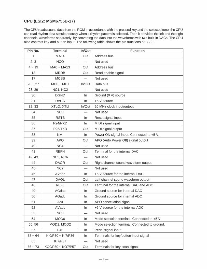
CPU (LSI2: MSM6755B-17)
The CPU reads sound data from the ROM in accordance with the pressed key and the selected tone; the CPUcan read rhythm data simultaneously when a rhythm pattern is selected. Then it provides the left and the rightchannels’ waveforms separately, by converting the data into the waveforms with two built-in DACs. The CPUalso controls key and button input. The following table shows the pin functions of LSI2.
Pin No. Terminal In/Out Function
1 MA14 Out Address bus
2, 3 NCO — Not used
4 ~ 19 MA0 ~ MA13 Out Address bus
13 MRDB Out Read enable signal
17 MCSB — Not used
20 ~ 27 MD0 ~ MD7 In/Out Data bus
28, 29 NC1, NC2 — Not used
30 DGND In Ground (0 V) source
31 DVCC In +5 V source
32, 33 XTLO, XTLI In/Out 20 MHz clock input/output
34 NC3 — Not used
35 RSTB In Reset signal input
36 P24/RXD In MIDI signal input
37 P25/TXD Out MIDI signal output
38 NMI In Power ON signal input. Connected to +5 V.
39 APO Out APO (Auto Power Off) signal output
40 NC4 — Not used
41 REFH Out Terminal for the internal DAC
42, 43 NC5, NC6 — Not used
44 DAOR Out Right channel sound waveform output
45 NC7 — Not used
46 AVdac In +5 V source for the internal DAC
47 DAOL Out Left channel sound waveform output
48 REFL Out Terminal for the internal DAC and ADC
49 AGdac In Ground source for internal DAC
50 AGadc In Ground source for internal ADC
51 ANI In APO cancellation signal
52 AVadc In +5 V source for the internal ADC
53 NC8 — Not used
54 MOD0 In Mode selection terminal. Connected to +5 V.
55, 56 MOD1, MOD2 In Mode selection terminal. Connected to ground.
57 P40 In Pedal signal input
58 ~ 64 KI0/P30 ~ KI7/P36 In Terminals for key/button input signal
65 KI7/P37 — Not used
66 ~ 73 KO0/P50 ~ KO7/P57 Out Terminals for key scan signal
— 5 —
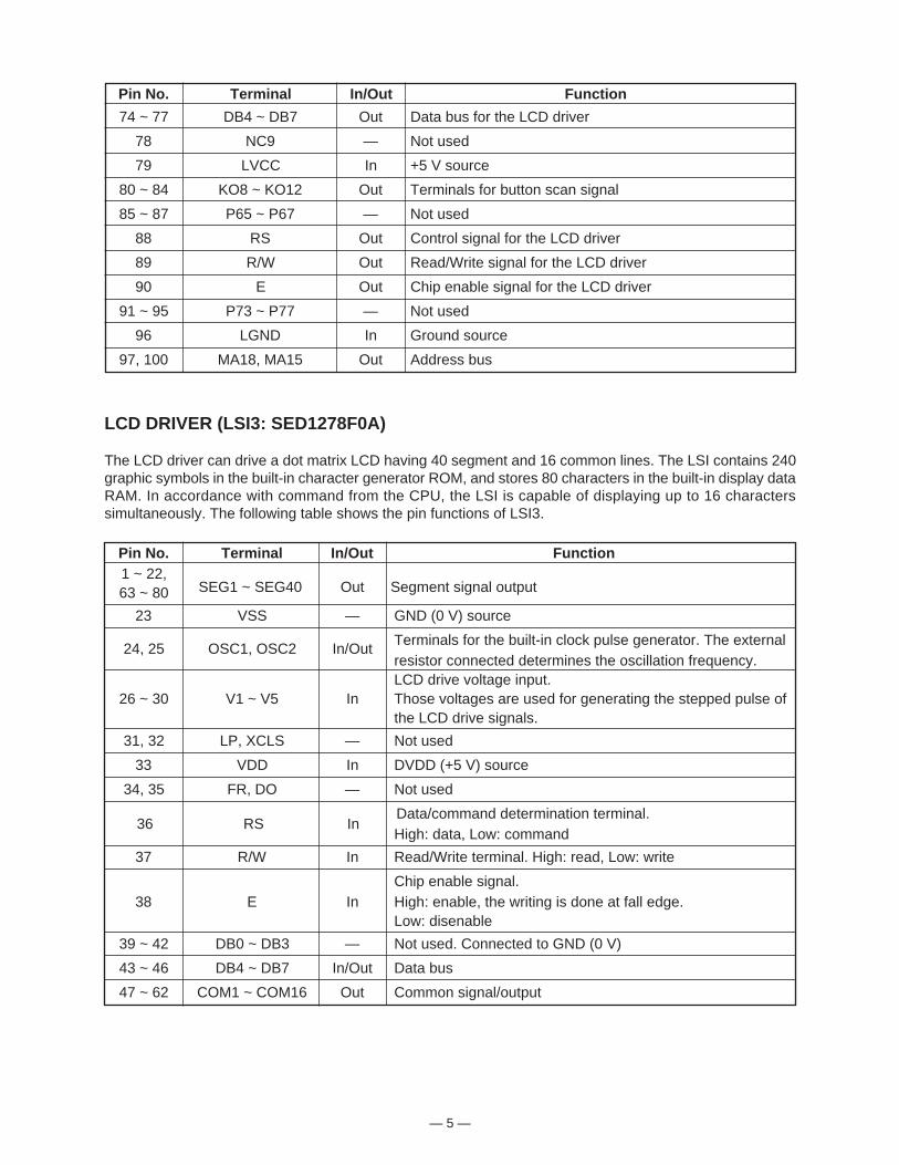
LCD DRIVER (LSI3: SED1278F0A)
The LCD driver can drive a dot matrix LCD having 40 segment and 16 common lines. The LSI contains 240graphic symbols in the built-in character generator ROM, and stores 80 characters in the built-in display dataRAM. In accordance with command from the CPU, the LSI is capable of displaying up to 16 characterssimultaneously. The following table shows the pin functions of LSI3.
Pin No. Terminal In/Out Function
74 ~ 77 DB4 ~ DB7 Out Data bus for the LCD driver
78 NC9 — Not used
79 LVCC In +5 V source
80 ~ 84 KO8 ~ KO12 Out Terminals for button scan signal
85 ~ 87 P65 ~ P67 — Not used
88 RS Out Control signal for the LCD driver
89 R/W Out Read/Write signal for the LCD driver
90 E Out Chip enable signal for the LCD driver
91 ~ 95 P73 ~ P77 — Not used
96 LGND In Ground source
97, 100 MA18, MA15 Out Address bus
Pin No. Terminal In/Out Function1 ~ 22,63 ~ 80
23 VSS — GND (0 V) source
Terminals for the built-in clock pulse generator. The externalresistor connected determines the oscillation frequency.LCD drive voltage input.
26 ~ 30 V1 ~ V5 In Those voltages are used for generating the stepped pulse ofthe LCD drive signals.
31, 32 LP, XCLS — Not used
33 VDD In DVDD (+5 V) source
34, 35 FR, DO — Not used
Data/command determination terminal.High: data, Low: command
37 R/W In Read/Write terminal. High: read, Low: write
Chip enable signal.38 E In High: enable, the writing is done at fall edge.
Low: disenable
39 ~ 42 DB0 ~ DB3 — Not used. Connected to GND (0 V)
43 ~ 46 DB4 ~ DB7 In/Out Data bus
47 ~ 62 COM1 ~ COM16 Out Common signal/output
SEG1 ~ SEG40 Out Segment signal output
24, 25 OSC1, OSC2 In/Out
36 RS In
— 6 —
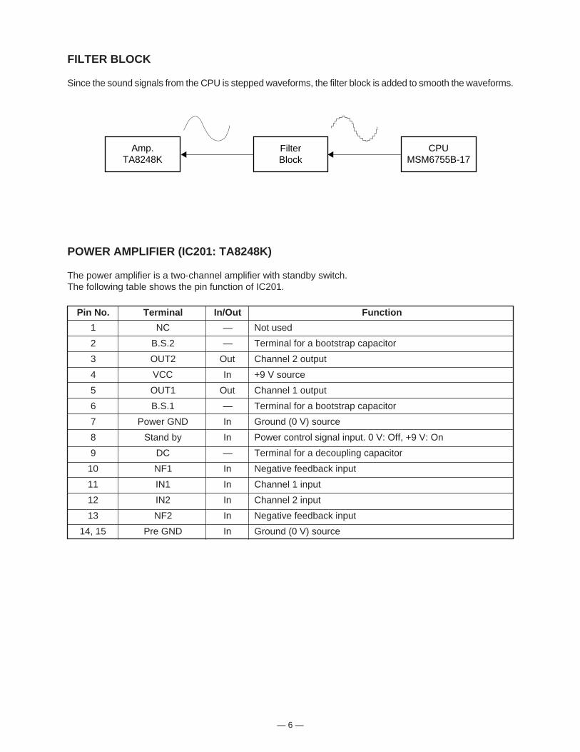
FILTER BLOCK
Since the sound signals from the CPU is stepped waveforms, the filter block is added to smooth the waveforms.
POWER AMPLIFIER (IC201: TA8248K)
The power amplifier is a two-channel amplifier with standby switch.The following table shows the pin function of IC201.
Pin No. Terminal In/Out Function
1 NC — Not used
2 B.S.2 — Terminal for a bootstrap capacitor
3 OUT2 Out Channel 2 output
4 VCC In +9 V source
5 OUT1 Out Channel 1 output
6 B.S.1 — Terminal for a bootstrap capacitor
7 Power GND In Ground (0 V) source
8 Stand by In Power control signal input. 0 V: Off, +9 V: On
9 DC — Terminal for a decoupling capacitor
10 NF1 In Negative feedback input
11 IN1 In Channel 1 input
12 IN2 In Channel 2 input
13 NF2 In Negative feedback input
14, 15 Pre GND In Ground (0 V) source
Amp.TA8248K
FilterBlock
CPUMSM6755B-17
— 7 —
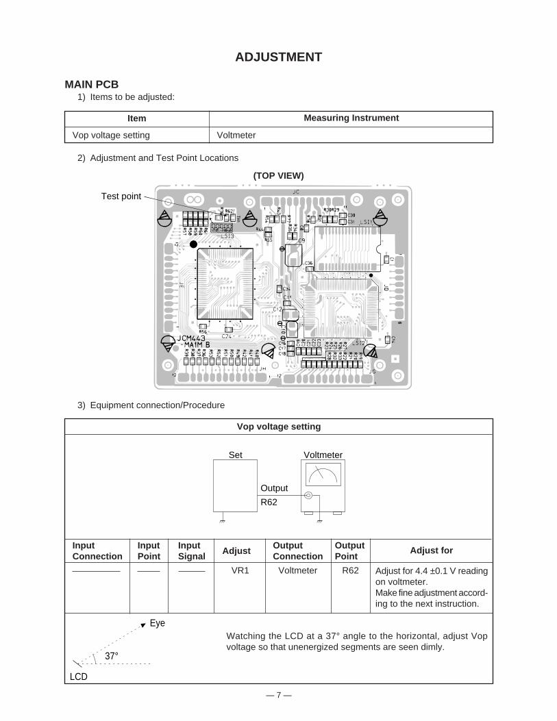
Output
Set Voltmeter
R62
3) Equipment connection/Procedure
Vop voltage setting
InputConnection
InputPoint
InputSignal
AdjustOutputConnection
OutputPoint
Adjust for
VR1 Voltmeter R62 Adjust for 4.4 ±0.1 V readingon voltmeter.Make fine adjustment accord-ing to the next instruction.
Watching the LCD at a 37° angle to the horizontal, adjust Vopvoltage so that unenergized segments are seen dimly.
ADJUSTMENT
MAIN PCB1) Items to be adjusted:
2) Adjustment and Test Point Locations
(TOP VIEW)
Item Measuring Instrument
Vop voltage setting Voltmeter
37°
LCD
Eye
Test point
— 8 —
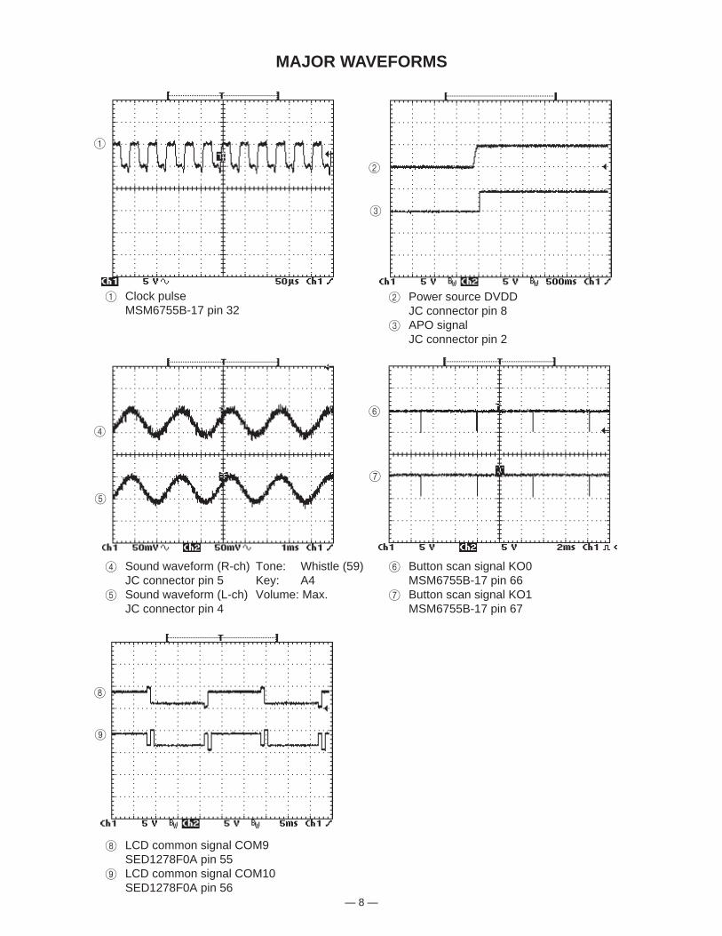
MAJOR WAVEFORMS
1 Clock pulseMSM6755B-17 pin 32
1
2 Power source DVDDJC connector pin 8
3 APO signalJC connector pin 2
2
3
4 Sound waveform (R-ch) Tone: Whistle (59)JC connector pin 5 Key: A4
5 Sound waveform (L-ch) Volume: Max.JC connector pin 4
4
5
6 Button scan signal KO0MSM6755B-17 pin 66
7 Button scan signal KO1MSM6755B-17 pin 67
6
7
8 LCD common signal COM9SED1278F0A pin 55
9 LCD common signal COM10SED1278F0A pin 56
8
9
— 9 —
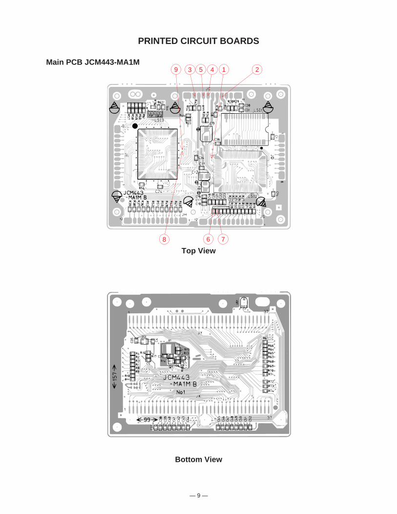
PRINTED CIRCUIT BOARDS
Main PCB JCM443-MA1M
Top View
Bottom View
5 213 4
8
9
6 7
— 11 —
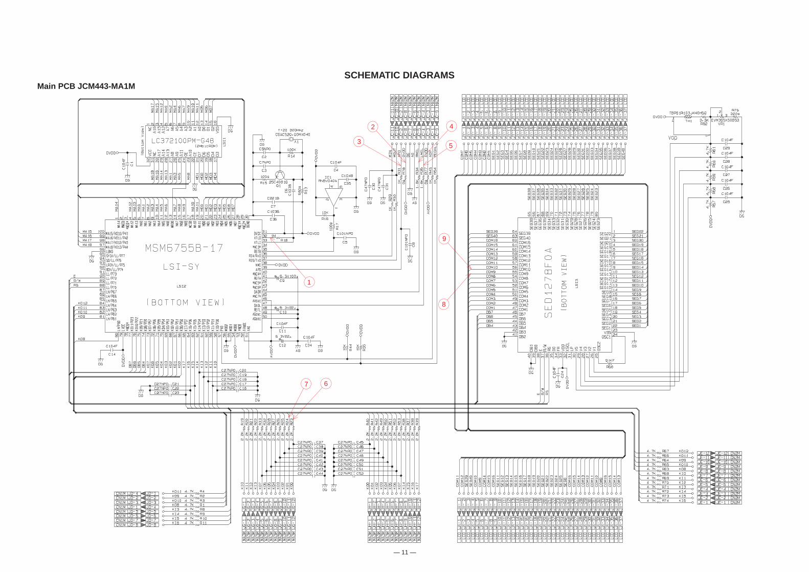
SCHEMATIC DIAGRAMSMain PCB JCM443-MA1M
1
7 6
2
3
4
5
9
8
— 12 —
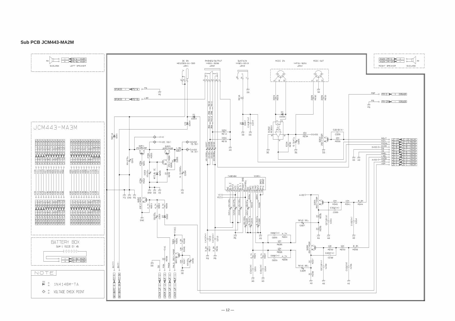
Sub PCB JCM443-MA2M

— 13 —
Console PCBs JCM443-CN1M/CN2M
— 14 —
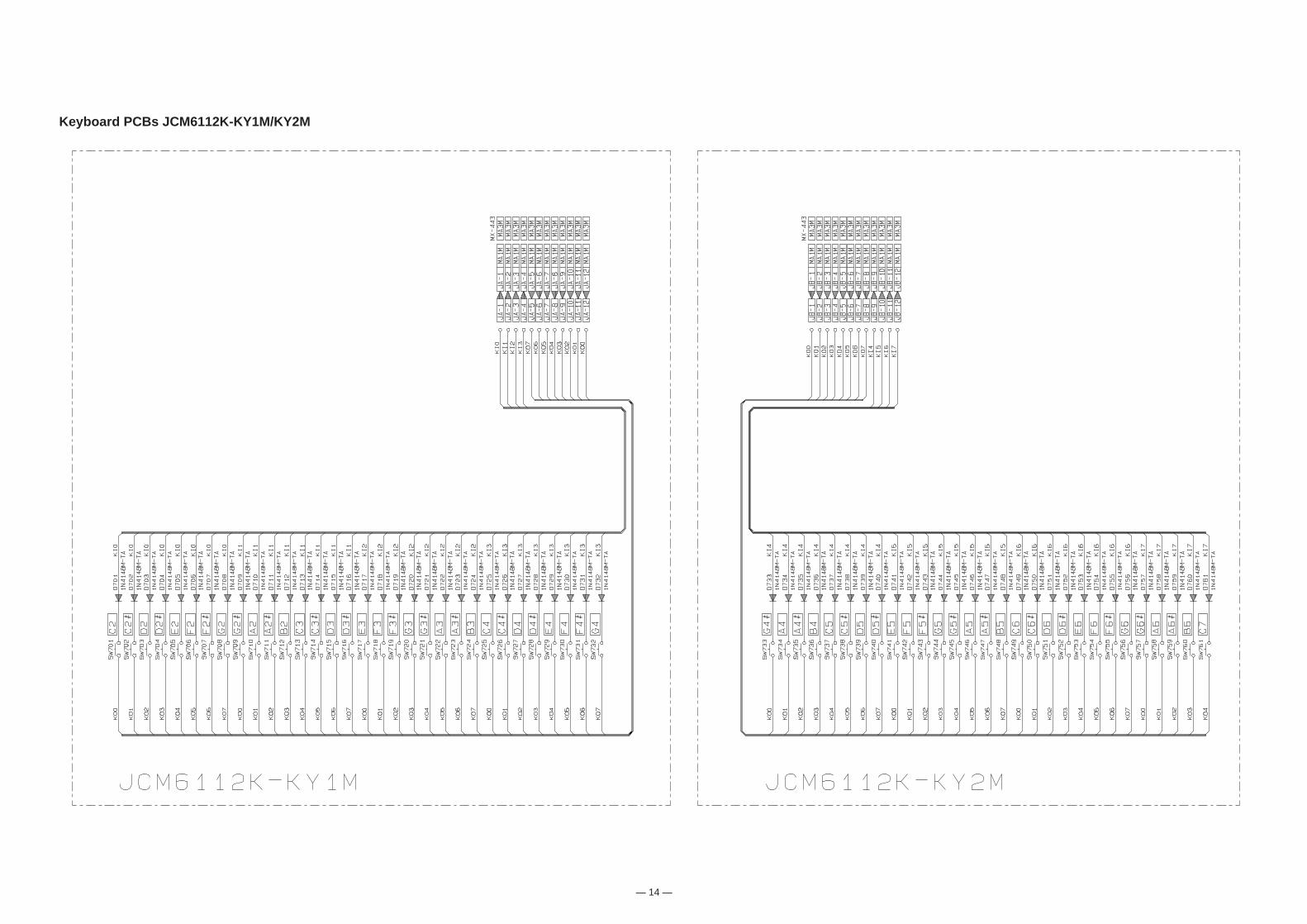
Keyboard PCBs JCM6112K-KY1M/KY2M
— 15 —
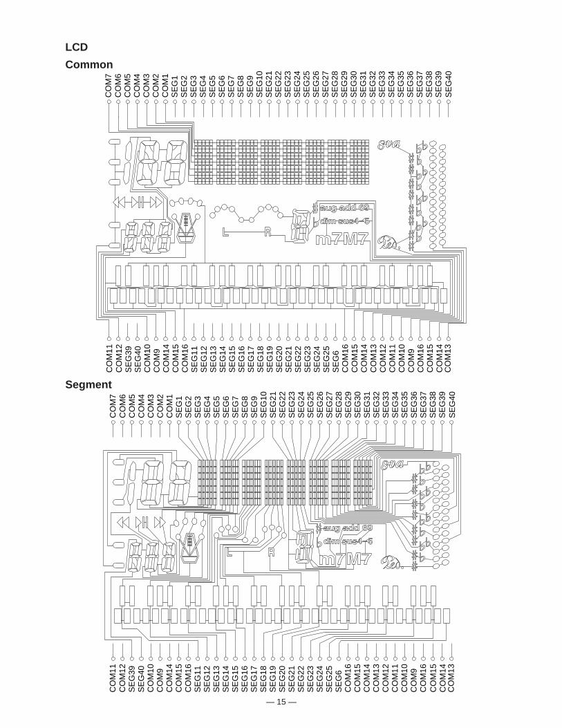
LCD
Common
Segment
CO
M7
CO
M6
CO
M5
CO
M4
CO
M3
CO
M2
CO
M1
SE
G1
SE
G2
SE
G3
SE
G4
SE
G5
SE
G6
SE
G7
SE
G8
SE
G9
SE
G10
SE
G21
SE
G22
SE
G23
SE
G24
SE
G25
SE
G26
SE
G27
SE
G28
SE
G29
SE
G30
SE
G31
SE
G32
SE
G33
SE
G34
SE
G35
SE
G36
SE
G37
SE
G38
SE
G39
SE
G40
CO
M11
CO
M12
SE
G39
SE
G40
CO
M10
CO
M9
CO
M14
CO
M15
CO
M16
SE
G11
SE
G12
SE
G13
SE
G14
SE
G15
SE
G16
SE
G17
SE
G18
SE
G19
SE
G20
SE
G21
SE
G22
SE
G23
SE
G24
SE
G25
SE
G6
CO
M16
CO
M15
CO
M14
CO
M13
CO
M12
CO
M11
CO
M10
CO
M9
CO
M16
CO
M15
CO
M14
CO
M13
CO
M7
CO
M6
CO
M5
CO
M4
CO
M3
CO
M2
CO
M1
SE
G1
SE
G2
SE
G3
SE
G4
SE
G5
SE
G6
SE
G7
SE
G8
SE
G9
SE
G10
SE
G21
SE
G22
SE
G23
SE
G24
SE
G25
SE
G26
SE
G27
SE
G28
SE
G29
SE
G30
SE
G31
SE
G32
SE
G33
SE
G34
SE
G35
SE
G36
SE
G37
SE
G38
SE
G39
SE
G40
CO
M11
CO
M12
SE
G39
SE
G40
CO
M10
CO
M9
CO
M14
CO
M15
CO
M16
SE
G11
SE
G12
SE
G13
SE
G14
SE
G15
SE
G16
SE
G17
SE
G18
SE
G19
SE
G20
SE
G21
SE
G22
SE
G23
SE
G24
SE
G25
SE
G6
CO
M16
CO
M15
CO
M14
CO
M13
CO
M12
CO
M11
CO
M10
CO
M9
CO
M16
CO
M15
CO
M14
CO
M13

— 16 —
EXPLODED VIEW13
13
16
1718
1920
21
15
22
23
R-1
R-2
2 4
3
1
6
5
8
7
9
14
10
12
11
R-3
Notes: This parts list does not include the cosmetic parts, whichparts are marked with item No. "R-X" in the explodedview.Contact our spare parts department if you need theseparts for refurbish.
1. Prices and specifications are subject to change with-out prior notice.
2. As for spare parts order and supply, refer to the"GUIDEBOOK for Spare parts Supply", publishedseperately.
3. The numbers in item column correspond to the samenumbers in drawing.
PARTS LIST
CTK-501
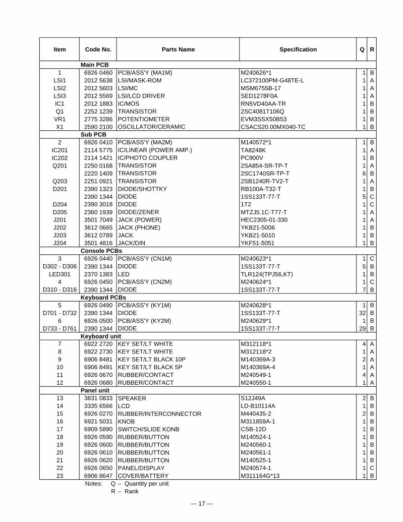
Item Code No. Parts Name Specification Q R
Main PCB1 6926 0460 PCB/ASS'Y (MA1M) M240626*1 1 B
LSI1 2012 5638 LSI/MASK-ROM LC372100PM-G48TE-L 1 ALSI2 2012 5603 LSI/MC MSM6755B-17 1 ALSI3 2012 5569 LSI/LCD DRIVER SED1278F0A 1 AIC1 2012 1883 IC/MOS RN5VD40AA-TR 1 BQ1 2252 1239 TRANSISTOR 2SC4081T106Q 1 B
VR1 2775 3286 POTENTIOMETER EVM3SSX50B53 1 BX1 2590 2100 OSCILLATOR/CERAMIC CSACS20.00MX040-TC 1 B
Sub PCB2 6926 0410 PCB/ASS'Y (MA2M) M140572*1 1 B
IC201 2114 5775 IC/LINEAR (POWER AMP.) TA8248K 1 AIC202 2114 1421 IC/PHOTO COUPLER PC900V 1 BQ201 2250 0168 TRANSISTOR 2SA854-SR-TP-T 1 A
2220 1409 TRANSISTOR 2SC1740SR-TP-T 6 BQ203 2251 0921 TRANSISTOR 2SB1240R-TV2-T 1 AD201 2390 1323 DIODE/SHOTTKY RB100A-T32-T 1 B
2390 1344 DIODE 1SS133T-77-T 5 CD204 2390 3018 DIODE 1T2 1 CD205 2360 1939 DIODE/ZENER MTZJ5.1C-T77-T 1 AJ201 3501 7049 JACK (POWER) HEC2305-01-330 1 AJ202 3612 0665 JACK (PHONE) YKB21-5006 1 BJ203 3612 0789 JACK YKB21-5010 1 BJ204 3501 4816 JACK/DIN YKF51-5051 1 B
Console PCBs3 6926 0440 PCB/ASS'Y (CN1M) M240623*1 1 C
D302 - D306 2390 1344 DIODE 1SS133T-77-T 5 BLED301 2370 1383 LED TLR124(TPJ56,KT) 1 B
4 6926 0450 PCB/ASS'Y (CN2M) M240624*1 1 CD310 - D316 2390 1344 DIODE 1SS133T-77-T 7 B
Keyboard PCBs5 6926 0490 PCB/ASS'Y (KY1M) M240628*1 1 B
D701 - D732 2390 1344 DIODE 1SS133T-77-T 32 B6 6926 0500 PCB/ASS'Y (KY2M) M240629*1 1 B
D733 - D761 2390 1344 DIODE 1SS133T-77-T 29 BKeyboard unit
7 6922 2720 KEY SET/LT WHITE M312118*1 4 A8 6922 2730 KEY SET/LT WHITE M312118*2 1 A9 6906 8481 KEY SET/LT BLACK 10P M140369A-3 2 A10 6906 8491 KEY SET/LT BLACK 5P M140369A-4 1 A11 6926 0670 RUBBER/CONTACT M240549-1 4 A12 6926 0680 RUBBER/CONTACT M240550-1 1 A
Panel unit13 3831 0833 SPEAKER S12J49A 2 B14 3335 6566 LCD LD-B10114A 1 B15 6926 0270 RUBBER/INTERCONNECTOR M440435-2 2 B16 6921 5031 KNOB M311859A-1 1 B17 6909 5890 SWITCH/SLIDE KONB CSB-12D 1 B18 6926 0590 RUBBER/BUTTON M140524-1 1 B19 6926 0600 RUBBER/BUTTON M240560-1 1 B20 6926 0610 RUBBER/BUTTON M240561-1 1 B21 6926 0620 RUBBER/BUTTON M140525-1 1 B22 6926 0650 PANEL/DISPLAY M240574-1 1 C23 6906 8647 COVER/BATTERY M311164G*13 1 B
Notes: Q – Quantity per unitR – Rank
— 17 —
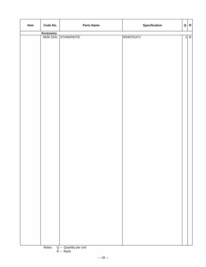
Item Code No. Parts Name Specification Q R
Accessory6926 1541 STAND/NOTE M340701A*1 1 B
Notes: Q – Quantity per unitR – Rank
— 18 —

MA0600571A