small-signal modeling of the boost converter operated in...
TRANSCRIPT

1 • Chris Basso – CM Boost Study
Small-Signal Modeling of the Boost Converter Operated in CM
Christophe Basso
IEEE Senior Member
2 • Chris Basso – – CM Boost Study
Course Agenda
The PWW Switch Concept
Small-Analysis in Continuous Conduction Mode
Small-Signal Response in Discontinuous Mode
EMI Filter Output Impedance
Cascaded Converters Operation
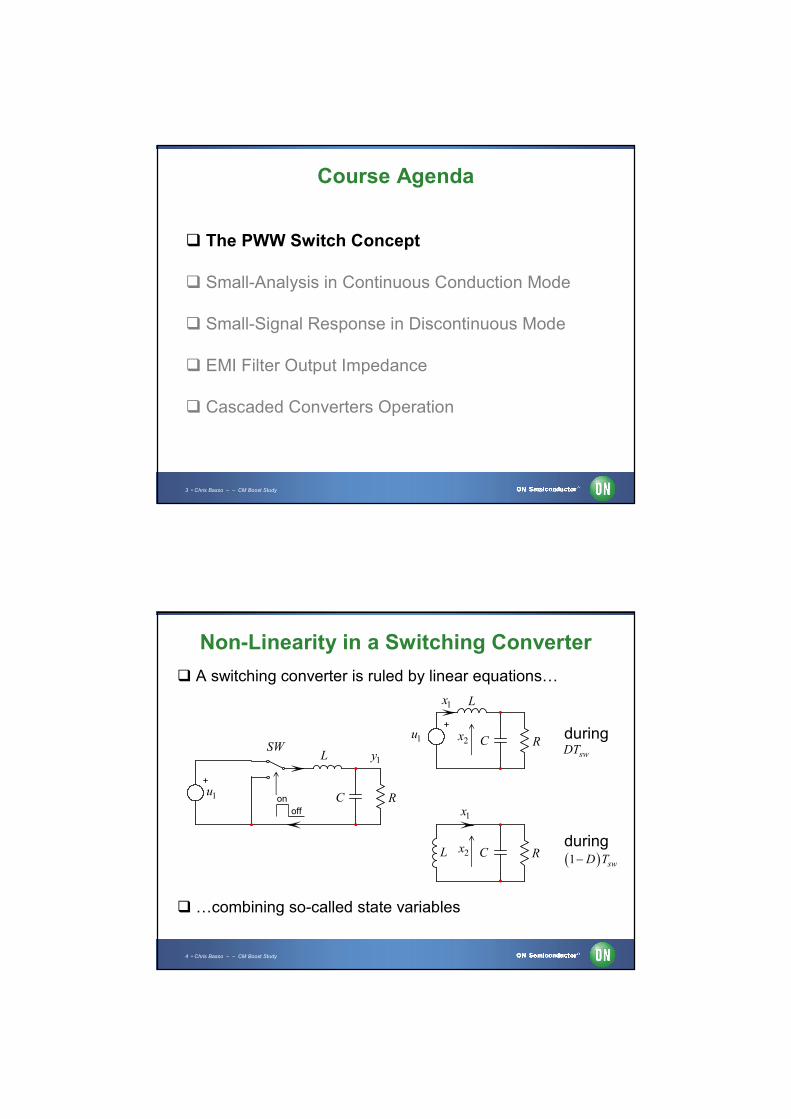
3 • Chris Basso – – CM Boost Study
Course Agenda
The PWW Switch Concept
Small-Analysis in Continuous Conduction Mode
Small-Signal Response in Discontinuous Mode
EMI Filter Output Impedance
Cascaded Converters Operation
4 • Chris Basso – – CM Boost Study
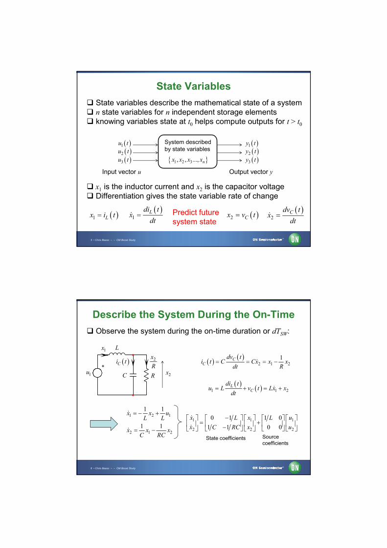
Non-Linearity in a Switching Converter
A switching converter is ruled by linear equations…
…combining so-called state variables
SWL
C R1u
1u
L
C R
L C R
1y
during
during 1 swD T
swDT
on
off
1x
1x
2x
2x
5 • Chris Basso – – CM Boost Study
State Variables
State variables describe the mathematical state of a system n state variables for n independent storage elements knowing variables state at t0 helps compute outputs for t > t0
System described by state variables
1 2 3, , ..., nx x x x
1u t
2u t
3u t
1y t
2y t
3y t
Input vector u Output vector y
x1 is the inductor current and x2 is the capacitor voltage Differentiation gives the state variable rate of change
1
Ldi tx
dt Predict future
system state 1 Lx i t
2
Cdv tx
dt 2 Cx v t
6 • Chris Basso – – CM Boost Study
Describe the System During the On-Time
Observe the system during the on-time duration or dTSW:
1 1 2
LC
di tu L v t Lx x
dt
2 1 2
1CC
dv ti t C Cx x x
dt R
1x
Ci t 2x
R
RC 2x
1 2 1
2 1 2
1 1
1 1
x x uL L
x x xC RC
1u
1 1 1
2 2 2
0 1 1 0
1 1 0 0
x x uL L
x x uC RC
State coefficients Source coefficients
L

7 • Chris Basso – – CM Boost Study
Describe the System During the Off-Time
Repeat the exercise during the off-time duration or 1-dTSW
1x
Ci t
2xRCL Lv t
1Lv t Lx 2Lv t x
2 1x Lx
Ri t
1 1 2R Ci t x i t x Cx
2 Rx i t R
2 1 2x R x Cx
1 2
2 1 2
10
1 1
x xL
x x xC RC
1 1 1
2 2 2
0 1 0 0
1 1 0 0
x x uL
x x uC RC
State coefficients Source coefficients
8 • Chris Basso – – CM Boost Study
Make it Fit the State Equation Format
Arrange expressions to make them fit the format:
x x t u t A B
1 1 1
2 2 2
0 1 1 0
1 1 0 0
x x uL L
x x uC RC
1 1 1
2 2 2
0 1 0 0
1 1 0 0
x x uL
x x uC RC
1 1
0 1 1 0
1 1 0 0
L L
C RC
A B
2 2
0 1 0 0
1 1 0 0
L
C RC
A B
on-time network
off-time network
How do we link matrixes A1 and A2, B1 and B2? We smooth the discontinuity by weighting them by D and 1-D
1 2 1 21 1x D D x t D D u t A A B B
State equation

9 • Chris Basso – – CM Boost Study
The State-Space Averaging Method (SSA)
We now have a continuous large-signal equation We need to linearize it via perturbations
0ˆD D d 0 ˆx x x 0 ˆu u u
1 2 1 21 1x D D x t d D u t A A B B
01 2 1 10
2 1 2
ˆ1ˆ ˆ ˆ
1 1ˆ ˆ ˆ
D dx x u u
L L L
x x xC RC
C
L
2x
0D d
1x
1u
10ˆu d
Canonical small-signal model
10 • Chris Basso – – CM Boost Study
The State-Space Averaging Method (SSA)
SSA was applied to switching converters by Dr Ćuk in 1976 It is a long, painful process, manipulating numerous terms What if you add an EMI filter for instance?
4 state variables and you have to re-derive all equations!
SW2L
2C R1u
1y1L
1C on
off
1L
1C2L
2C R
2L 2C R
1L
1C
1u
1u

11 • Chris Basso – – CM Boost Study
The PWM Switch Model in Voltage Mode
We know that non-linearity is brought by the switching cell
L
Why don't we linearize the cell alone?
1u C R
d
a c
PWM switch VM p
a
p
c
a
p
c
a: activec: commonp: passive
Switching cell Small-signal model(CCM voltage-mode)
. .
V. Vorpérian, "Simplified Analysis of PWM Converters using Model of PWM Switch, parts I and II"IEEE Transactions on Aerospace and Electronic Systems, Vol. 26, NO. 3, 1990
12 • Chris Basso – – CM Boost Study
Replace the Switches by the Model
Like in the bipolar circuit, replace the switching cell…
L
1u C R
a
p
c
…and solve a set of linear equations!
. . L1u C R
..

13 • Chris Basso – – CM Boost Study
d
a c
PWM switch VM p
dac
PW
M s
witc
h V
Mp
dac
PW
M s
witc
h V
Mp
dac
PW
M s
witc
h V
Mp
An Invariant Model
The switching cell made of two switches is everywhere!
buck
buck-boost
boost
Ćuk
d
a c
PWM switch VM p
14 • Chris Basso – – CM Boost Study
Smoothing the Discontinuity
A CRT TV displays frames at a certain rate, 50 per second
1 23
4 5 6 7
8
910
The optic nerve time constant is larger than an interval A succession of discrete events is seen as continuous
11
12
See "phi phenomena", www.wikipedia.org
Low-frequency filteringIntegration
1t
15 • Chris Basso – – CM Boost Study
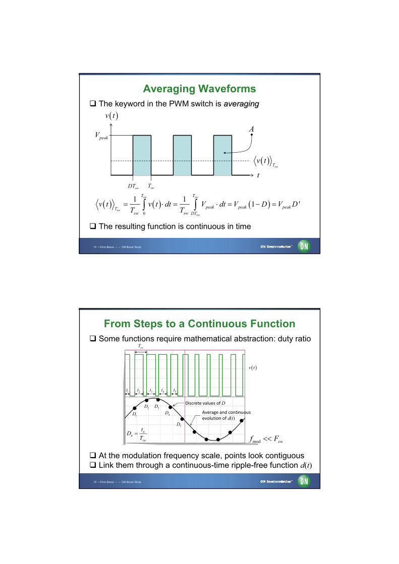
Averaging Waveforms
The keyword in the PWM switch is averagingaveraging
t
v t
A
swDT
swT
v t
0
1 11 '
sw sw
sw
sw
T T
peak peak peakTsw sw DT
v t v t dt V dt V D V DT T
swT
peakV
The resulting function is continuous in time
16 • Chris Basso – – CM Boost Study
From Steps to a Continuous Function
Some functions require mathematical abstraction: duty ratio
At the modulation frequency scale, points look contiguous Link them through a continuous-time ripple-free function d(t)
swT
1t 2t 3t 4t 5t
v t
1D
Discrete values of D2D 3D
4D
5D
nn
sw
tD
T
mod swf F
Average and continuous evolution of d(t)

17 • Chris Basso – – CM Boost Study
The Common Passive Configuration
The PWM switch is a single-pole double-throw model
a c
p
d
'd
C R
L
inV
ci t ai t
apv t cpv toutV
Install it in a buck converter and draw the waveforms
a c
p
d
'd ai t ci t
apv t cpv t
CCM
18 • Chris Basso – – CM Boost Study
The Common Passive Configuration
Average the current waveforms across the PWM switch
ai t
ci t
0
0
t
t
swDT
sw
c Ti t
sw
c Ti t
0
1 sw
sw sw
dT
a a a c cT Tsw
i t I i t dt D i t DIT
a cI DI
Averagedvariables
CCM

19 • Chris Basso – – CM Boost Study
The Common Passive Configuration
Average the voltage waveforms across the PWM switch
cpv t
apv t
0
0
t
t
swDT
sw
ap Tv t
sw
cp Tv t
0
1 sw
sw sw
dT
cp cp cp ap apT Tsw
v t V v t dt D v t DVT
cp apV DV
Averagedvariables
CCM
20 • Chris Basso – – CM Boost Study
A Two-Port Representation
We have a link between input and output variables
Two-portcell
a
p
c
p
cDI cI
apDVapV
It can further be illustrated with current and voltage sources
a
p
c
p
cI
apDVapV
aI
cpVcDI
d
d
CCM

21 • Chris Basso – – CM Boost Study
A Transformer Representation
The PWM switch large-signal model is a dc "transformer"!
It can be immediately plugged into any 2-switch converter
a c
p
1 D
cIaI
ac
II
Da cI DI
cp
ap
VV
D cp apV DV
dc equations!
. .
1
D..
LLr
inV C Ra
cp
CCM
22 • Chris Basso – – CM Boost Study
Simulate Immediately with this Model
SPICE can get you the dc bias point
4
L1100u
C1470u
R110
7
Vg10
Rdum1u
a
Vout5
VICR2100m
c c
V(a,p)*V(d)
p p
a
V(d)*I(VIC)V30.3AC = 1
d
9.80V14.0V
10.0V
300mV
9.80V
-40.0
-20.0
0
20.0
40.0
10 100 1k 10k 100k
-360
-180
0
180
360
…but also the ac response as it linearizes the circuitdB °
Hz
H f
arg H f
CCM

23 • Chris Basso – – CM Boost Study
We Want Transfer Functions
Derive the dc transfer function: open caps., short inductors
1
D
.Lr
inV Ra
c
p
aI
cIcI
.
outV
cpV
out outV I R
outI
out a cV I I R
a cI DI
1out cV I D R
in L c cp outV r I V V
in L c out outV r I DV V
1out in
c
L
V D VI
r
1
11
out
Lin
V
rVD
D R
2
1 1
'1
'
out
Lin
V
rV D
RD
CCM
24 • Chris Basso – – CM Boost Study
Plotting Transfer Functions
Plot the lossy boost transfer function in a snapshot
0 0.2 0.4 0.6 0.8 10
1
2
3
4
5
f d 0.1( )
f d 0.2( )
f d 0.3( )
f d 0.4( )
f d 0.5( )
f d 0.6( )
f d 0.7( )
f d 0.8( )
f d 0.9( )
f d 1( )
d
0.1ΩLr
0.2ΩLr
1ΩLr
out
in
V
V
Duty ratio
10ΩR
Above a certain conversion ratio, latch-up occursCCM

25 • Chris Basso – – CM Boost Study
Course Agenda
The PWW Switch Concept
Small-Analysis in Continuous Conduction Mode
Small-Signal Response in Discontinuous Mode
EMI Filter Output Impedance
Cascaded Converters Operation
26 • Chris Basso – – CM Boost Study
A Boost Converter in Current Mode
Identify the diode and switch position in a boost CM
vc
a c
PWM switch CM p
duty-cycle
Replace switches by the small-signal PWM switch model
Current mode
a
pc

27 • Chris Basso – – CM Boost Study
A Small Signal Model
The model includes current sources and conductances
1o
i
kR
'
2sw
f o
DD Tg Dg
L
1'
2sw a
o
n
T Sg D D
L S
i
i
Dk
R c
i f
ap
Ig D g
V
cr o
ap
Ig g D
V
1
ig
a c
p
ˆc iv k ˆ
cp rv g ˆap fv g ˆ
c ov k1
og sC
cI
V. Vorpérian,"Analysis of Current-Controlled PWM Converters using the Model of the PWM Switch", PCIM Conference ,1990
28 • Chris Basso – – CM Boost Study
Start with a Large Signal Response
Use the original large-signal (nonlinear) PWMCM model
5 V/1 AFsw = 1 MHz
1
2
Cout200uF
Resr60m
Vin2.7
4 5
L15u
7
duty_ratio
Vout
R41.5m
R91k
Rload1v
cac
PW
M s
witch
CM
p
duty
-cyc
le
X4PWMCCMCML = 5uFs = 1MegRi = -50mSe = 0
V1471mAC = 1
Vin
5.00V
5.00V
2.70V
2.69V
2.69V
462mV
471mV

29 • Chris Basso – – CM Boost Study
Frequency Response of the CM Boost
This frequency response becomes the reference
1.00
13.0
25.0
37.0
49.0
10 100 1k 10k 100k 1Meg
frequency in hertz
-324
-252
-180
-108
-36.0
out
c
V f
V f
out
c
V f
V f
(dB)
(°)
Subharmonicpoles0 14.5 dBH
30 • Chris Basso – – CM Boost Study
Plug the Linearized Small-Signal Model
Use the linearized model to check coefficients and response
4
C2
Cs
VIC
parameters
Fsw =1Meg
Tsw =1/Fsw
L=5u
Cs=1/(L*(Fsw *3.14)^2)
Ri=-50m
Se=0
Vin=2.7
Vout=5
Sn=(Vac/L)*Ri
Sf=(Vap/L)*Ri
Vc=471m
Vac=-Vin
Vap=-Vout
Vcp=(-Vout+Vin)
Ic=(Vc/Ri)-D*Tsw *Se-Vcp*(1-D)*Tsw /(2*L)
D=Vcp/Vap
D'=1-D
ki=D/Ri
gi=D*(gf-Ic/Vap)
gr=(Ic/Vap)-go*D
ko=1/Ri
go=(Tsw /L)*(D'*Se/Sn+0.5-D)
gf=D*go-(D*D')*Tsw /(2*L)
B3
Current
V(a,p)*gf
B4
Current
V(v c)*ko
c
B5
Current
V(v c)*ki
B6
Current
V(c,p)*gr
R4
1/gi
R5
1/go
15
L2
L
16
C3
200uF
R3
1v c
R6
60m
Vout
R7
1u
B2
Voltagev (c,p)/v (a,p)
1
R8
1.5m
a
p
a
p
c
Vin
Vin
V2
471m
AC = 1
D
2.69V 5.00V
2.69V
4.30uV
2.69V
0V
462mV
2.70V
471mV
These coefficients arecomputed by the macro

31 • Chris Basso – – CM Boost Study
Small-Signal Response and Original Model
Validate the small-signal approach by comparing responses
1.00
13.0
25.0
37.0
49.0
10 100 1k 10k 100k 1Meg
frequency in hertz
-324
-252
-180
-108
-36.0
out
c
V f
V f
out
c
V f
V f
(dB)
(°)
0 14.5 dBH
Good to go!
32 • Chris Basso – – CM Boost Study
Rearrange Sources to Improve Readability
It is important to lay the network out properly
4
C2
Cs
VIC
B3
Current
V(0,out)*gf
B4
Current
V(v c)*ko
B5
Current
V(v c)*ki
B6
Current
V(c,out)*gr
R4
1/gi
R5
1/go
15
L2
L
16
C3
200uF
R3
1v c
R6
60m
Vout
B2
Voltagev (c,out)/v (0,out)
1
R8
1.5m c
Vin
Vin
V2
471m
AC = 1
D
out
2.69V
2.69V
2.69V
0V
462mV
2.70V
471mV
5.00V
Make sure the frequency response remains unchanged
Storage element
Storage element
Storage element
33 • Chris Basso – – CM Boost Study
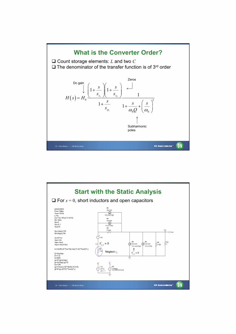
What is the Converter Order?
Count storage elements: L and two C The denominator of the transfer function is of 3rd order
1 2
1
0 2
0 0
1 11
1 1
z z
p
s s
s sH s H
s s ss Q
Dc gain
Subharmonicpoles
Zeros
34 • Chris Basso – – CM Boost Study
Start with the Static Analysis
For s = 0, short inductors and open capacitors
1
VIC
parametersFsw=1MegTsw=1/FswL=5uCs=1/(L*(Fsw*3.14)^2)Ri=-50mSe=0Vin=2.7Vout=5
Sn=(Vac/L)*RiSf=(Vap/L)*Ri
Vc=471mVac=-VinVap=-VoutVcp=(-Vout+Vin)
Ic=(Vc/Ri)-D*Tsw*Se-Vcp*(1-D)*Tsw/(2*L)
D=Vcp/VapD'=1-Dki=D/Rigi=D*(gf-Ic/Vap)gr=(Ic/Vap)-go*Dko=1/Rigo=(Tsw/L)*(D'*Se/Sn+0.5-D)gf=D*go-(D*D')*Tsw/(2*L)
B3
Current
V(0,out)*gf
B4
Current
V(vc)*ko
B5
Current
V(vc)*ki
B6
Current
V(c,out)*gr
R4
1/gi
R5
1/go
R3
1
vc
Vout
B2
Voltagev(c,out)/v(0,out)
R8
1.5m
c
V2
471m
AC = 1
D
out
Neglect rL
0c
V
0c
V

35 • Chris Basso – – CM Boost Study
Simplify and Rearrange
Rearrange sources to make the circuit look simpler
B3CurrentV(out)*gf
B4CurrentV(vc)*ko
B5CurrentV(vc)*ki
R41/gi
R51/go
R31
Vout
out
B1CurrentV(out)*gr
1
outout f c o out o i out r c i
VV g V k V g g V g V k
R
00
0
1
1i
f i r
k kH
g g g gR
H0 20 logko ki
gf go gi gr1
RL
14.563 dB
Mathcad® calculations
36 • Chris Basso – – CM Boost Study
Put Storage Elements Back in Place
C2Cs
B3Current
V(out)*gf
B4Current
V(vc)*koB5Current
V(vc)*ki
B6Current
V(c,out)*gr
R41/gi
R51/go
L2L
16
C3200uF
R31
vc R660m
Vout
cV2471mAC = 1
out
Rearrange sources to make the circuit look simpler
Label each storage element with a time constant Time to call the FACTs! Set excitation to 0, Vc = 0
FACTS: Fast Analytical Circuit TechniqueS
1
2
3

37 • Chris Basso – – CM Boost Study
Polynomial Form of a 3rd Function
A transfer function is made of a numerator and a denominator
N sH s
D s
zerospoles
The denominator combines the circuit time constants
1 1 2 2 1 12 31 2 3 1 2 1 3 2 3 1 2 31D s s s s
Time constantwith Cs
Time constantwith L
Time constantwith Cout
To calculate time constants, suppress the excitation, all is dc
38 • Chris Basso – – CM Boost Study
Calculate the First Time Constant
B3Current
V(out)*gf
B6Current
V(out)*gr
R41/gi
R51/go
R31
1
R660m
out
V20AC = 1
Vc
tau1
L shorted
tau3C open
R11f
R2100G
c
B5CurrentV(vc)*ki
B4CurrentV(vc)*ko
?R
= 0
= 0
What resistance does Cs « see » ?
The excitation is 0 so several sources go away You can further simplify the circuit and test it in SPICE

39 • Chris Basso – – CM Boost Study
Calculate the First Time Constant
Check the result with a simple dc operating point calculation
B3
Current
V(out)*gf
B6
CurrentV(out)*gr
R4
1/gi
R5
1/goR3
11
R6
60m
out
V2
0
AC = 1
Vctau1
L shorted
tau3C open
R1
1f
R2
100G
c
I1
1
V(vc)*ki
B5
Current
V(vc)*ko
B4
Current
R7
1/gi
R8
1/go
R9
1I2
1
out2
V(out2)*(gr-gf)
B2
Current
495mV
297f V
0V
495mVeqR
1
1 1|| ||eq L
i o
R Rg g
TVTI
outT out r f
eq
VI V g g
R
1
1outT
T Tr f
eq
VVR
I I g gR
1
1
Reqgr gf
0.495
1 sRC
40 • Chris Basso – – CM Boost Study
Calculate the Second Time Constant
B3Current
V(out)*gf
B4Current
V(vc)*koB5Current
V(vc)*ki
B6Current
V(c,out)*gr
R41/gi
R51/go
R31
vc
1
R660m
Vout
cV2471mAC = 1
out
tau3C open
tau1Cs open
What resistance does L « see » ?
?R
= 0
= 0
The excitation Vc is 0 so simplify the circuit Rearrange the network and test it in SPICE

41 • Chris Basso – – CM Boost Study
Calculate the Second Time Constant
B3
Current
V(out)*gf
B4
Current
V(vc)*koB5
CurrentV(vc)*ki
B6
Current
V(c,out)*gr
R4
1/gi
R5
1/go
R3
1
vc
Voutx
cV2
0
AC = 1
out
I1
1
B1
Current
V(out2)*gf
B8
Current
V(c1)*gr
R1
1/gi
R2
1/go
R6
1
Vout2
I2
1
out2
c1
R7
1/gr
0V
-52.9V
-48.8V
-52.9V -48.8V
TVTI T
T
VR
I
42 • Chris Basso – – CM Boost Study
Calculate the Second Time Constant
Express IT and Vout then rearrange to unveil VT/IT
0
1T out
T out f
V VI V g
g
out T T r eqV I V g R
1 eq f oT
T o eq r f o
R g gVR
I g R g g g
21 eq f o
o eq r f o
L
R g g
g R g g g
1 Req2 gf go go Req2 gr gf go
52.897 Same result as dc point simulation
2
1 1|| ||eq L
i r
R Rg g

43 • Chris Basso – – CM Boost Study
Calculate the Third Time Constant
What resistance does Cout « see » ?
B3
Current
V(out)*gf
B4
CurrentV(vc)*ko
B5
Current
V(vc)*ki
B6
CurrentV(c,out)*gr
R41/gi
R5
1/go
R3
1
vc
1
R6
60m
Vout
cV2
471mAC = 1
out
tau1Cs open
tau2L shorted
?R= 0
= 0
The circuit is very close to that of 1
Rearrange the network and test it in SPICE
44 • Chris Basso – – CM Boost Study
Calculate the Third Time Constant
R71/gi
R81/go
R91
out2
V(out2)*(gr-gf)
B2Current
6
R260m
I31
495mV
-60.0mV
Same resistance as for 1 plus rC in series
3
1
1
1 C out
r f
eq
r Cg g
R
1
1 1|| ||eq L
i o
R Rg g

45 • Chris Basso – – CM Boost Study
First Coefficients a1 and a2
FACTs tell us that a1 sums up all time constants
1 1 2 3a
V. Vorpérian, “Fast Analytical Techniques for Electrical and Electronic Circuits”, Cambridge Press, 2002
For a2, we multiply combined-time constants
Dimension is time
1 1 22 1 2 1 3 2 3a Dimension is time2
What is this new time constants definition, ?
12
sC (HF)
L C (dc)
?R
13
sC (HF)
L C(dc)
?R
23
L (HF)
C sC (dc)
?R
12
46 • Chris Basso – – CM Boost Study
Calculate the Terms for a2
B3
Current
V(out)*gf
B4
CurrentV(v c)*ko
B5
CurrentV(v c)*ki
B6
CurrentV(c,out)*gr
R4
1/gi
R5
1/goR3
11
R6
60m
out
V2
0
AC = 1
Vc
tau1
Cs HF
R?
tau3
C openR1
1u
I1
1
c
12
sC (HF)
L C (dc)
?R
What resistance does L while Cs is a short and Cout is open?
Go for an intermediate step
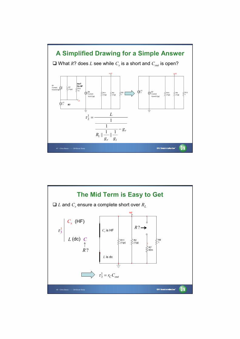
47 • Chris Basso – – CM Boost Study
A Simplified Drawing for a Simple Answer
What R? does L see while Cs is a short and Cout is open?
B1
Current
V(out2)*gf
B8
Current
V(c2)*gr
R2
1/gi
R7
1/go
R8
1
tau1Cs HF
R?
R10
1u
I2
1
R11
1/gr
out2
c2
R9
1/gi
R13
1
I3
1 R15
1/gr
out3
B7
Current
V(out3)*gr
12
1
1
1
1 1|| ||
r
r i
L
g
Rg g
48 • Chris Basso – – CM Boost Study
The Mid Term is Easy to Get
13
sC (HF)
L C(dc)
?R
R21/gi
R81
R111/gr
out
1
R760m
2
L and Cs ensure a complete short over RL
?R
13 C outr C
Cs is HF
L is dc
49 • Chris Basso – – CM Boost Study
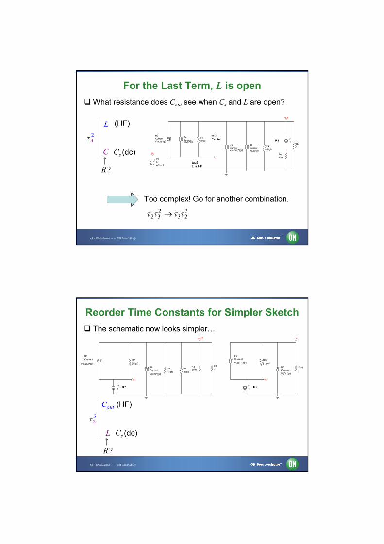
For the Last Term, L is open
23
L (HF)
C sC (dc)
?R
B3Current
V(out)*gf
B4
CurrentV(vc)*ko
B5CurrentV(vc)*ki
B6CurrentV(c,out)*gr
R4
1/gi
R51/go
R3
11
R660m
out
V2
0AC = 1
Vc
tau1Cs dc R?
tau2L is HF
I11
c
What resistance does Cout see when Cs and L are open?
Too complex! Go for another combination.
2 32 3 3 2
50 • Chris Basso – – CM Boost Study
Reorder Time Constants for Simpler Sketch
B1
Current
V(out2)*gf
B8
Current
V(c2)*gr
R1
1/gi
R2
1/goR7
1R8
60m
R?I2
1
out2
R9
1/gr
VT
B2
Current
V(out)*gf
B3
CurrentV(T)*gr
R3
1/go
Req
R?I1
1
VT
out
The schematic now looks simpler…
32
outC (HF)
L sC (dc)
?R
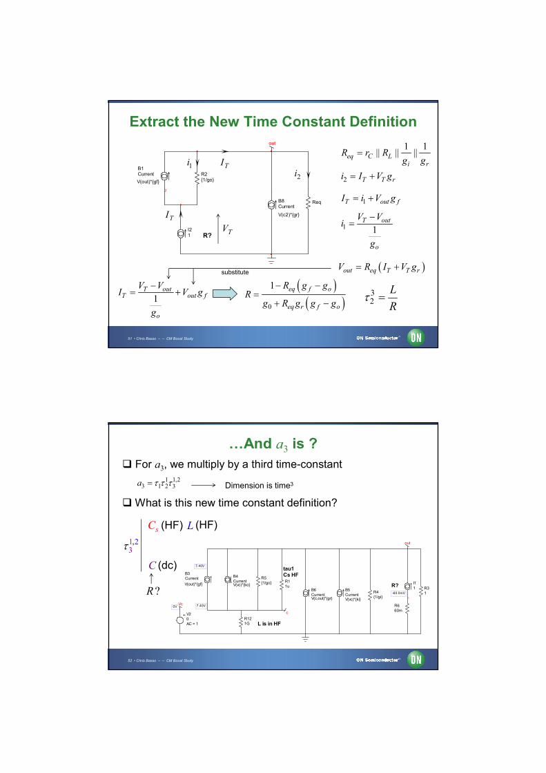
51 • Chris Basso – – CM Boost Study
Extract the New Time Constant Definition
1 1|| || ||eq C L
i r
R r Rg g
2 T T ri I V g
1T out fI i V g
1 1T out
o
V Vi
g
1T out
T out f
o
V VI V g
g
out eq T T rV R I V g
2
B1Current
V(out)*gf
B8Current
V(c2)*gr
R21/go
Req
R?I21
out
0
1 eq f o
eq r f o
R g gR
g R g g g
32
L
R
substitute
TI
TI
2i1i
TV
52 • Chris Basso – – CM Boost Study
…And a3 is ?
For a3, we multiply by a third time-constant
1 1,23 1 2 3a Dimension is time3
What is this new time constant definition?
231,
sC (HF)
C (dc)
?R
L (HF)
B3Current
V(out)*gf
B4CurrentV(vc)*ko
B5CurrentV(vc)*ki
B6CurrentV(c,out)*gr
R41/gi
R51/go
R31
1
R660m
out
V20AC = 1
Vc
tau1Cs HF
L is in HF
R?R11u
I11
c
R121G
7.40V
7.40V
-60.0mV
0V

53 • Chris Basso – – CM Boost Study
Rearrange and Simplify
B3
Current
V(out)*gf
B4
CurrentV(vc)*ko
B5
CurrentV(v c)*ki
B6
CurrentV(c,out)*gr
R4
1/gi
R5
1/goR3
11
R6
60m
out
V2
0
AC = 1
Vc
tau1Cs HF
L is in HF
R?R1
1uI1
1
c
R12
1G
parameters
Fsw =1Meg
Tsw =1/Fsw
L=5u
Cs=1/(L*(Fsw *3.14)^2)
Ri=-50m
Se=0
Vin=2.7
Vout=5
Sn=(Vac/L)*Ri
Sf=(Vap/L)*Ri
Vc=471m
Vac=-Vin
Vap=-Vout
Vcp=(-Vout+Vin)
Ic=(Vc/Ri)-D*Tsw *Se-Vcp*(1-D)*Tsw /(2*L)
D=Vcp/Vap
D'=1-D
ki=D/Ri
gi=D*(gf-Ic/Vap)
gr=(Ic/Vap)-go*D
ko=1/Ri
go=(Tsw /L)*(D'*Se/Sn+0.5-D)
gf=D*go-(D*D')*Tsw /(2*L)
6
R2
1/gi
R8
12
R9
60m
R?I2
1
7.40V
7.40V
-60.0mV
0V
7.40V
-60.0mV 1,23
1|| L C out
i
r r Cg
54 • Chris Basso – – CM Boost Study
Final Denominator Expression
1
2
1 12
1 1
1 11s C out
eq f or f r f
eq eqo eq r f o
La C r C
R g gg g g gR R
g R g g g
2
2
1 1 10 2
1
1 1 1
1 1 1 1 11
1 1|| ||
s s C out C out
eq f or f r f r f
eq eq eqr eq r f o
r i
L La C C r C r C
R g gg g g g g gR R Rg g R g g g
Rg g
1 1 2 3a
1 1 2 1 1 32 1 2 1 3 2 3 1 2 1 3 3 2a
1 123 1 2 3a 3
1
1
1 1||
1 1
1
1 1|| ||
s L C outi
r feq
r
r i
La C r r C
gg gR g
Rg g

55 • Chris Basso – – CM Boost Study
C2
Cs
B3
CurrentV(out)*gf
B4
CurrentV(vc)*ko
B5
CurrentV(vc)*ki
B6
CurrentV(c,out)*gr
R4
1/gi
R5
1/go
L2
L
1
C3
200uF
R3
1
vc R6
60m
Vout
c
V2
471m
AC = 1
out
Find the Zeros
A zero means the excitation does not generate a response
pIcI
No response means that:
0pI 1pI I 0C outr sC Short circuit
1
1z
C out
sr C
0pI 0outV
cI
aI1I
56 • Chris Basso – – CM Boost Study
Find the Zeros
C2
Cs
B3
CurrentV(out)*gf
B4
CurrentV(vc)*ko
B5
CurrentV(vc)*ki
B6
CurrentV(c,out)*gr
R4
1/gi
R5
1/go
L2
L
1
C3
200uF
R3
1
vc R6
60m
Vout
c
V2
471m
AC = 1
out
A Capitalize on the 0-V response to remove sources
pIcI
cI
aI
0
rcv g
a pI I r c i ccv g V k I
c c o o sc cI V k v g v sC
r c i c o o sc c cv g V k V k v g v sC
c
c o o sc c
vV k v g v sC
sL
1c o
c
o s
V kv
g sCsL

57 • Chris Basso – – CM Boost Study
Find The Zeros
After substituting v(c) into the equation rearrange it
2
2 21 1
c i o i r o s i c o
o s o s
V k Lg k s Lg k s C Lk s V k
sLg s C L sLg s C L
2i o i r o s i ok Lg k s Lg k s C Lk s k
21 0o i r o s ii o
i o i o
g k g k C Lkk k sL s
k k k k
21 0o i r o s i
i o i o
g k g k C LksL s
k k k k
For low Q values, the 2nd order polynomial can expressed as
2 21 2 1
1
1 1 1a
a s a s a s sa
58 • Chris Basso – – CM Boost Study
Find the Zeros – Final Lap!
The first zero is a right half-plane zero
1
1 1o i r
i o z
og k g k
ks
k
sL
s
Negative value!
1
i oz
o i r o
k ks
L g k g k
1
21 L
z
D R
L
The second zero is given by the capacitor ESR
1 0C outsr C
The third zero is located at high frequency
3
1 1s i
o i r o z
C k ss
g k g k s
3
o i r oz
s i
g k g ks
C k
Neglect it
2
21 L
z
D R
L
fz2
z2
23.16 10
4 kHz
V. Vorpérian,“Analytical Methods in Power Electronics", 3-day course in Toulouse,2004

59 • Chris Basso – – CM Boost Study
Arranging the Transfer Function
The denominator has to be rearranged a little bit…
2 31 2 31D s b s b s b s
The term 1+b1s dominates at low frequency
2 3 2321 2 3 1
1 1
1 1 1bb
b s b s b s b s s sb b
1
2321 2
1 1
11 1 1
1p
n p n
bb sb s s s
b b s s
Q
1
3
21sw a
L np
out
T S
R SLM
C
1
' 0.5p
c
Qm D
nswT
1 a
cn
Sm
S
Dc gain H0
0
2
1
12
2
L
i L sw a
n
RH
R R T SM
SLM
60 • Chris Basso – – CM Boost Study
Final Expression
The transfer function of a CCM Boost Converter in CM is
2
2
2
3
1 111 1
1 12 1221
C out
Lout L
outc i L sw a
sw an n p n
L n
Ls sr C
D RV s R
CV s R R T S s ssMT SSLM Q
R SLM
Sa is the external ramp compensation to damp subharmonic oscillations

61 • Chris Basso – – CM Boost Study
Check SPICE Versus Mathcad
10 100 1 103
1 104
1 105
1 106
0
20
40
20 log H1 i 2 fk 10
fk
10 100 1 103
1 104
1 105
1 106
100
0
100
arg H1 i 2 fk 180
fk
Full-featured transfer functions versus SPICE
Simplified transfer functions versus SPICE
10 100 1 103
1 104
1 105
1 106
0
20
40
20 log H1 i 2 fk 10
20 log H2 i 2 fk 10
fk
10 100 1 103
1 104
1 105
1 106
100
0
100
arg H1 i 2 fk 180
arg H2 i 2 fk 180
fk
out
c
V s
V s
out
c
V s
V s
out
c
V s
V s
out
c
V s
V s
62 • Chris Basso – – CM Boost Study
Course Agenda
The PWW Switch Concept
Small-Analysis in Continuous Conduction Mode
Small-Signal Response in Discontinuous Mode
EMI Filter Output Impedance
Cascaded Converters Operation

63 • Chris Basso – – CM Boost Study
The CM Boost Converter in DCM
To check the operating mode, calculate the critical load
2
2
2
1
sw outcrit
inin
out
F LVR
VV
V
1 MHz
5 µH
2.7 V
5 V
sw
in
out
F
L
V
V
74.7 ΩcritR
CCM, RL < Rcrit
DCM, RL > Rcrit
Li t
t
t
sw
L Ti t
,L peakI
,valleyLI
,L peakI
,valley 0LI deadtime
64 • Chris Basso – – CM Boost Study
Transfer Function of DCM CM Boost
The converter is a first-order converter at low frequency
1 2
1 2
1 121 1
2 11 1
z zout
n c sw
p p
s s
V MH s
S m T D M s s
inn i
VS R
L
1
1z
C outr C
2 2load
z
R
M L
1
1 2 1
1p
L out
M
R C M
2
21
12p sw
MFD
1 ac
n
Sm
S

65 • Chris Basso – – CM Boost Study
The Ac Response of the DCM CM Boost
10 100 1 103
1 104
1 105
1 106
40
20
0
20
40
20 log H3 i 2 fk 10
fk
10 100 1 103
1 104
1 105
1 106
100
0
100
arg H3 i 2 fk 180
fk
A RHPZ is still present in DCM with a high-frequency pole
SPICE simulation versus Mathcad
out
c
V s
V s
out
c
V s
V s
66 • Chris Basso – – CM Boost Study
Why a RHP Zero in DCM?
The RHP Zero is present in CCM and is still there in DCM!
Tsw
D1Tsw
Id(t)
t
D2Tsw
D3Tsw
iL,peak
When D1 increases, [D1,D2] stays constant but D3 shrinks
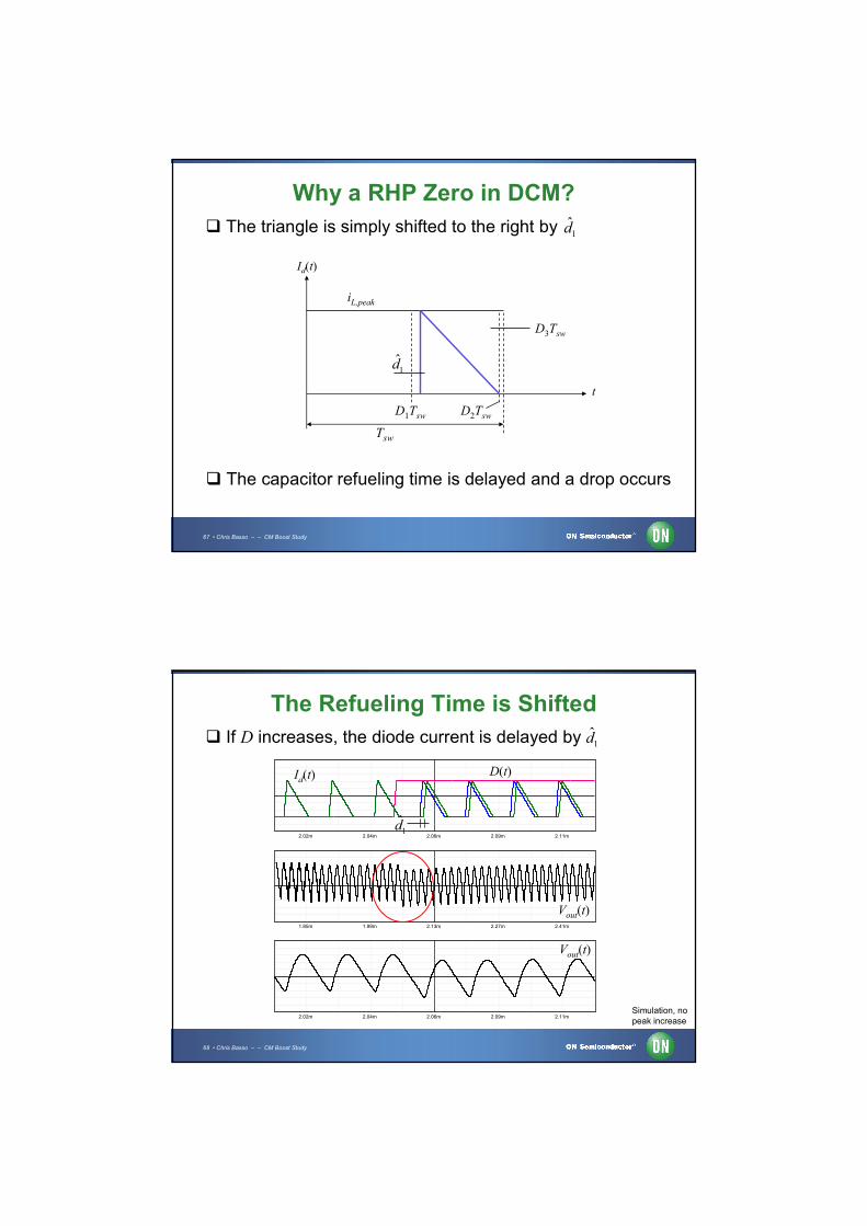
67 • Chris Basso – – CM Boost Study
Why a RHP Zero in DCM?
The triangle is simply shifted to the right by 1d
The capacitor refueling time is delayed and a drop occurs
Tsw
D1Tsw
t
D2Tsw
D3Tsw
1d
iL,peak
Id(t)
68 • Chris Basso – – CM Boost Study
The Refueling Time is Shifted
If D increases, the diode current is delayed by 1d
2.02m 2.04m 2.06m 2.09m 2.11m
1.85m 1.99m 2.13m 2.27m 2.41m
2.02m 2.04m 2.06m 2.09m 2.11m
Vout(t)
Vout(t)
1d
Id(t)D(t)
Simulation, no peak increase

69 • Chris Basso – – CM Boost Study
Course Agenda
The PWW Switch Concept
Small-Analysis in Continuous Conduction Mode
Small-Signal Response in Discontinuous Mode
EMI Filter Output Impedance
Cascaded Converters Operation
70 • Chris Basso – – CM Boost Study
EMI Filter Interaction
A LC filter is included to prevent the dc line pollution
gVloadR
outVL
C
inV
Switching converter
gVloadR
outVL
C
inV
Switching converter
C. Basso, “Designing Control Loops for Linear and Switching Power Supplies”, Artech House, 2012
What load does the converter offer?
?Z s

71 • Chris Basso – – CM Boost Study
A Negative Incremental Resistance
Assume a 100%-efficient converter:
out inP P in in out outI V I V
In closed-loop operation, Pout is constant
2
out
in in in out
in in in
Pd
dI V V P
dV dV V
outin in
in
PI V
V
For a constant Pout , if Vin increases, Iin drops
10 15 20 25 300.2
0.4
0.6
0.8
1
VinV
AinI
10 15 20 25 300.2
0.4
0.6
0.8
1
VinV
AinI
The incremental input resistance is negative
72 • Chris Basso – – CM Boost Study
A Simple LC Filter
The low-pass filter is built with a L and C components:
1
1z
Cr C
Lr LCr
C
gV
1
2
0 0
1
1
zsT s
s s
Q
0
1 L
C
r R
r RLC
0 C
load
L C L C
LC r R CQ R
L C r r r R r R L
If R is || with -R R R C
QR R L
R
A negative resistance cancels losses: poles become imaginary

73 • Chris Basso – – CM Boost Study
A Negative Impedance Oscillator
If losses are compensated, the damping factor is zero
2
20 0
1
1
T ss s
Q
1
2Q
If ohmic losses are gone, the damping factor is zero, Q is infinite.
Without precautions, instability can happen!
3.64m 10.9m 18.2m 25.5m 32.7m
70.0
90.0
110
130
150
Output voltage
> 0 0
< 0
3.64m 10.9m 18.2m 25.5m 32.7m
70.0
90.0
110
130
150
> 0 0
< 0
Input voltage
Lr
inV
Cr
C
L
I
out
out
PI
V Negative resistance
(constant)
74 • Chris Basso – – CM Boost Study
Filter Output Impedance
What is the output impedance of an LC filter?
L
Lr
Cr
C
R
TV s
TI s
0out
N sZ s R
D s
Ω ΩNo dimension
It follows the form
2
1 1
||
1 ||
C out
Lout L load
C loadL load C
L load L load
Ls sr C
rZ s r R
r RLs C r R r s LC
r R r R

75 • Chris Basso – – CM Boost Study
Negative Resistance at Low Frequency Neg. resistance exists because of feedback (Pout = constant )
16
4
Cout200uF
Resr60m
7
Vin2.7
3 18
L15u
6
R1Rupper
R310k
1
V22.5
9
Verr
2
duty_cycle
vout
5
R41.5m
14
R610k
R71k
X2AMPSIMPVHIGH = 100VLOW = 10m
R91k
SwitchMode Power Supplies: SPICE Simulations and Practical DesignsChristophe Basso - McGraw-Hill, 2014
11
D1mbra210et3
13
Rdson140m
parameters
Rupper=10kfc=8k
pm=70Gfc=-20
pfc=-101
G=10^(-Gfc/20)boost=pm-(pfc)-90
pi=3.14159K=tan((boost/2+45)*pi/180)
C2=1/(2*pi*fc*G*k*Rupper)C1=C2*(K^2-1)
R2=k/(2*pi*fc*C1)
fp=1/(2*pi*R2*C2)fz=1/(2*pi*R2*C1)
15
R2R2
C1C1
C2C2
vca
cL
ossy
PW
M
swit
ch C
M
p
duty
-cyc
le
SW
D
PWMCM2_LX1L = 5uFs = 1MegRi = -40mSe = 16.4k
VZin
I1AC = 1
L210GH
Rload55.00V
5.00V
2.70V
2.70V2.70V
2.50V
2.50V
1.10V
536mV
99.9mV
-455mV-301mV
2.50V
2.70V
76 • Chris Basso – – CM Boost Study
Negative Resistance at Low Frequency The resistance is truly negative up to 200 Hz
1 2
-24.0
-12.0
0
12.0
24.0
10 100 1k 10k 100k 1Meg
-144
-72.0
0
72.0
144
inZ f
inZ f
(dBΩ)
(°)
180inZ
1.02 Ω
In this regionPout constant
77 • Chris Basso – – CM Boost Study
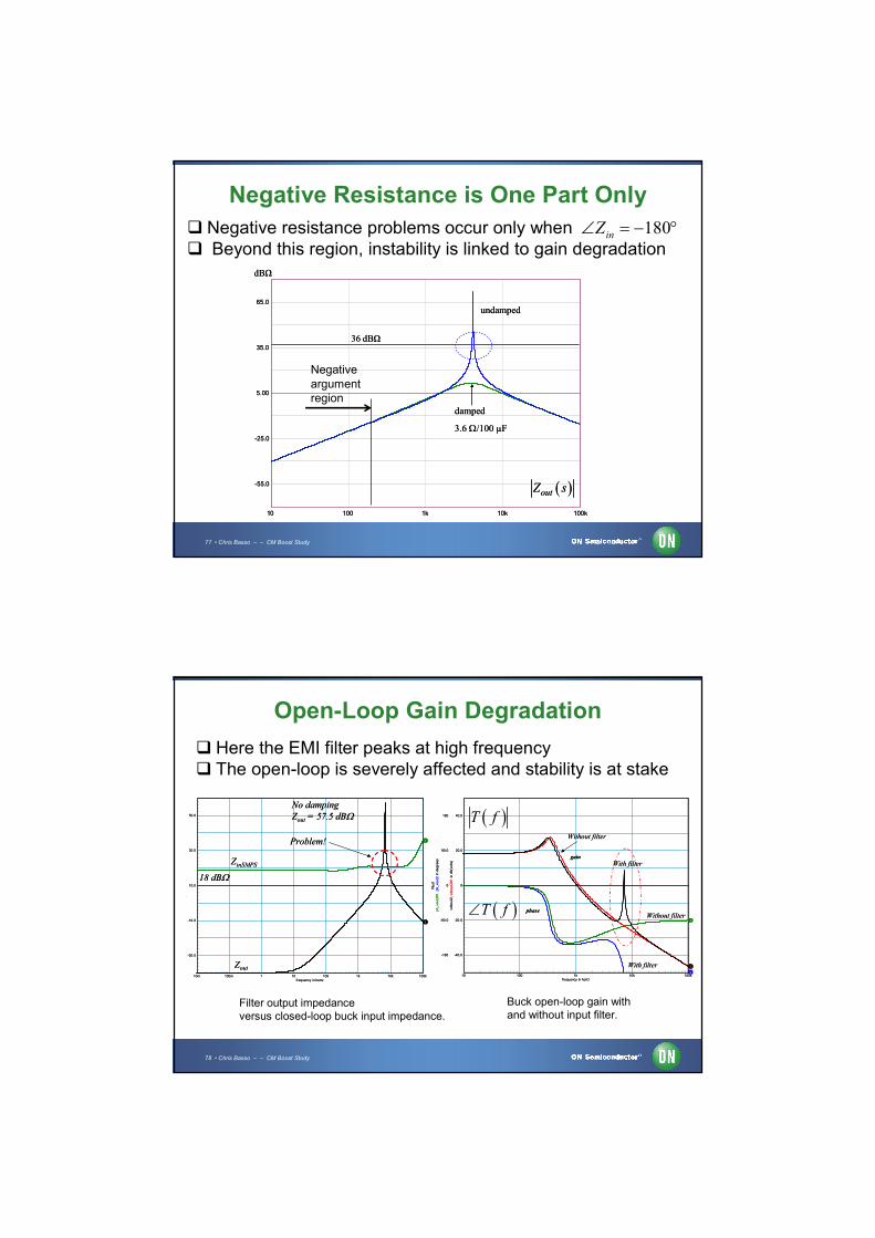
Negative Resistance is One Part Only
10 100 1k 10k 100k
-55.0
-25.0
5.00
35.0
65.0
36 dBΩ
outZ s
dBΩ
undamped
damped
3.6 /100 µF
10 100 1k 10k 100k
-55.0
-25.0
5.00
35.0
65.0
36 dBΩ
outZ s
dBΩ
undamped
damped
3.6 /100 µF
Negative resistance problems occur only when Beyond this region, instability is linked to gain degradation
180inZ
Negative argumentregion
78 • Chris Basso – – CM Boost Study
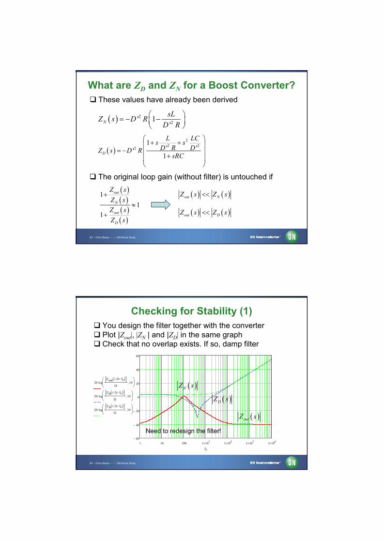
Open-Loop Gain Degradation
10m 100m 1 10 100 1k 10k 100kfrequency in hertz
-30.0
-10.0
10.0
30.0
50.0
p in
1 /
am
pe
re
1
7
Zout
No dampingZout = 57.5 dB
ZinSMPS
18 dB
Problem!
10m 100m 1 10 100 1k 10k 100kfrequency in hertz
-30.0
-10.0
10.0
30.0
50.0
p in
1 /
am
pe
re
1
7
Zout
No dampingZout = 57.5 dB
ZinSMPS
18 dB
Problem!
10 100 1k 10k 100kfrequency in hertz
-40.0
-20.0
0
20.0
40.0
vdbout2
, vd
bout2
#1
in d
b(v
olts
)
-180
-90.0
0
90.0
180
ph_vo
ut2
#1,
ph_vo
ut2
in d
egre
es
Plo
t1
2
3
41
phase
gain
With filter
With filter
Without filter
Without filter
10 100 1k 10k 100kfrequency in hertz
-40.0
-20.0
0
20.0
40.0
vdbout2
, vd
bout2
#1
in d
b(v
olts
)
-180
-90.0
0
90.0
180
ph_vo
ut2
#1,
ph_vo
ut2
in d
egre
es
Plo
t1
2
3
41
phase
gain
With filter
With filter
Without filter
Without filter
Filter output impedanceversus closed-loop buck input impedance.
Buck open-loop gain withand without input filter.
T f
T f
Here the EMI filter peaks at high frequency The open-loop is severely affected and stability is at stake

79 • Chris Basso – – CM Boost Study
Evaluating How Loop Gain is Modified
outZ s inZ s
ˆgv
ˆoutv
H s
G sd
The converter transfer function is evaluated at Zout = 0
0in
out
V s
V sT s H s G s
D s
ˆ 0inv For Zout = 0
80 • Chris Basso – – CM Boost Study
In reality, the EMI output impedance makes The converter ac input voltage is no longer zero
0outZ s
outZ s ˆoutv
H s
G sd
ˆoutv
G sd
Considering the Filter Output Impedance
0outZ
0outZ
ˆ 0inv H s
0in
out
V s
V sT s
D s
0in
out
V s
V sT s
D s

81 • Chris Basso – – CM Boost Study
Extra Element Theorem to Help
It can be shown how an EMI affects the open-loop gain:
ˆoutv
H s
G sd
outZ s
0out
out
Z s
V sT s
D s
Gain without the filter
outZ s Filter output impedance
0 0
1
1out out
out
out out N
outZ s Z s
D
Z s
V s V s Z sT s
Z sD s D s
Z s
82 • Chris Basso – – CM Boost Study
What are ZD and ZN?
ZD and ZN come from the Extra Element Theorem, EET
0D i D s
Z s Z s
Open-loop input impedance
0out
N i V sZ s Z s
Input impedance for 0outV s
0 35%
ˆ 0
D
d
?DZ s
ˆ 0
out
out
V
v
0 35%
ˆ 0
D
d
ˆ 0
out
out
V
v
?NZ s
ˆ 0outi ˆ 0outi
Open-loop input impedance Input impedance for 0outV s Ideal control
Null
83 • Chris Basso – – CM Boost Study
What are ZD and ZN for a Boost Converter?
These values have already been derived
2
2' 1
'N
sLZ s D R
D R
2
2 22
1' ''
1D
L LCs s
D R DZ s D RsRC
The original loop gain (without filter) is untouched if
1
1
1
out
N
out
D
Z s
Z s
Z s
Z s
out NZ s Z s
out DZ s Z s
84 • Chris Basso – – CM Boost Study
Checking for Stability (1)
You design the filter together with the converter Plot |Zout|, |ZN | and |ZD| in the same graph Check that no overlap exists. If so, damp filter
1 10 100 1 103
1 104
1 105
1 106
60
40
20
0
20
40
60
20 logZout i 2 fk
10
20 logZD i 2 fk
10
20 logZN i 2 fk
10
fk
Need to redesign the filter!
NZ s
DZ s
outZ s

85 • Chris Basso – – CM Boost Study
Checking for Stability (2)
You design the filter after the converter Plot |Zout|, |Zin | in the same graph Check that no overlap exists. If so, damp filter
10m 100m 1 10 100 1k 10k 100kfrequency in hertz
-30.0
-10.0
10.0
30.0
50.0
7
654321
Zout
ZinSMPS
18 dB
Ok, margin is 8 dB min
Rdamp= 1
Rdamp= 2
Rdamp= 3
Rdamp= 4
Rdamp= 5
10m 100m 1 10 100 1k 10k 100kfrequency in hertz
-30.0
-10.0
10.0
30.0
50.0
7
654321
Zout
ZinSMPS
18 dB
Ok, margin is 8 dB min
Rdamp= 1
Rdamp= 2
Rdamp= 3
Rdamp= 4
Rdamp= 5
Dampingnetwork
R damps
C cuts dc
86 • Chris Basso – – CM Boost Study
Course Agenda
The PWW Switch Concept
Small-Analysis in Continuous Conduction Mode
Small-Signal Response in Discontinuous Mode
EMI Filter Output Impedance
Cascaded Converters Operation
87 • Chris Basso – – CM Boost Study
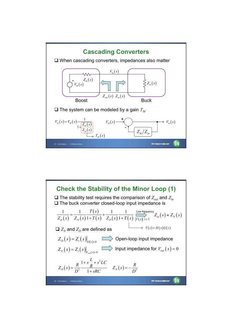
Cascading Converters
When cascading converters, impedances also matter
thZ s
thV s inZ s
Boost Buck
thV s
inV s
inV s+
-th inZ Z
The system can be modeled by a gain TM
1
1in th
th
in
V s V sZ s
Z s
MT s
outZ s inZ s
88 • Chris Basso – – CM Boost Study
Check the Stability of the Minor Loop (1)
The stability test requires the comparison of Zout and Zin
The buck converter closed-loop input impedance is
1 1 1 1
1 1in N D
T s
Z s Z s T s Z s T s
0D i D s
Z s Z s
Open-loop input impedance
0out
N i V sZ s Z s
Input impedance for 0outV s
ZN and ZD are defined as
2
2
1
1D
Ls s LC
R RZ sD sRC
2N
RZ s
D
in NZ s Z sLow frequency
1T s
T s H s G s

89 • Chris Basso – – CM Boost Study
Use SPICE Models First Simulate the boost converter output impedance
16
C5
820u
R10
18m3
Vin
11
12
L1
33u
1
R1
11.66k
R3
1.35k
6
8
X2
AMPSIMP
VHIGH = 10
VLOW = 10m
V2
2.5
Verr
2
duty_cycle
5
Rload
8.3
voutvout
11
vca
c
PW
M s
witc
h C
Mp
duty
-cyc
le
X3
PWMCM
L = 33u
Fs = 200k
Ri = -300m
Se = 82k
9
R2
50k
C2
10n
R5
7m
C3
282p
R4
1m
I1
AC = 1A
11-15 V/24 V – 3 A
1 10 100 1k 10k 100k 1Meg
-80.0
-60.0
-40.0
-20.0
0 outZ f
(dBΩ)
Closed-loop Zout
90 • Chris Basso – – CM Boost Study
Use SPICE Models First Simulate the buck converter input impedance
Vout
2
Cout
820u
Resr
14m1
V4
24
3 4
L1
8u
7
5
duty_cycle
R4
4m
R2
416m
vout
vc
a c
PWM switch CM p
duty-cyc le
6
PWMCM
X2
L = 8u
Fs = 200k
Ri = 176m
Se = 30k
9
R1
1k
R3
1k
10
V2
2.5
11
Verr
vout
8
R6
15k
C1
3.5n
C3
1n
R7
1m
L2
1kH
Zin
I1
AC = 1
5.00V
5.00V
24.0V
5.05V 5.05V
210mV
24.0V
2.37V
2.50V
2.50V
2.37V
2.37V
24 V/5 V – 12 A
Closed-loop Zin
(dBΩ)
10 100 1k 10k 100k 1Meg
18.2
18.6
19.0
19.4
19.8
inZ f

91 • Chris Basso – – CM Boost Study
Compare Magnitude Curves
10 100 1k 10k 100k 1Meg
-41.0
-21.0
-1.00
19.0
39.0
(dBΩ)
inZ f
outZ f
No overlap
92 • Chris Basso – – CM Boost Study
Compare Phase Curves
1 10 100 1k 10k 100k 1Meg
-90.0
0
90.0
180
270
inZ f
outZ f
(°)
Neg. up to 1 kHz

93 • Chris Basso – – CM Boost Study
Check Minor Loop Gain
1 10 100 1k 10k 100k 1Meg
-360
-270
-180
-90.0
0
-80.0
-70.0
-60.0
-50.0
-40.0
dB °
out
in
Z f
Z f
out
in
Z f
Z f
There is no gain, . The system is stableout inZ Z
94 • Chris Basso – – CM Boost Study
With Cascaded Converters
16
4
C5
820u
R10
18m
3
Vin
11
12
L1
33u
1
R1
11.66k
R3
1.35k
6
7
X2
AMPSIMP
VHIGH = 10
VLOW = 10m
V2
2.5
VerrBoost
2
dc_boost
VoBoost
11
vca
c
PW
M s
witc
h C
Mp
du
ty-c
ycle
X3
PWMCM
L = 33u
Fs = 200k
Ri = -300m
Se = 82k
9
R2
50k
C2
10n
R5
7m
C3
282p
VoBuck
13
Cout
820u
19
Resr
14m
14 15
L2
8u
18
10
dc_buck
R4
4m v out
vc
a c
PWM switch CM p
duty-cycle
PWMCM
X1
L = 8u
Fs = 200k
Ri = 176m
Se = 30k
21
R9
1k
R11
1k
22
V3
2.5
23
VerrBuck
v out
24
R6
15k
C1
3.5n
C6
1n
R7
1m
I1
unknown
Iout
24.1V
24.1V
11.0V
11.0V
2.50V
2.50V
2.02V
545mV
11.0V
2.50V
5.00V
5.00V
5.05V 5.05V
209mV
2.37V
2.50V
2.50V
2.37V
2.37VBoost
Buck

95 • Chris Basso – – CM Boost Study
Check Transient Response
4.90
4.95
5.00
5.05
5.10
100u 300u 500u 700u 900u
23.90
23.95
24.00
24.05
24.10
Transient response is good for the buck
(V)
(V)
outv t
outv t
Buck
Boost
Iout from 5 to 12 A in 1 µs
96 • Chris Basso – – CM Boost Study
Literature
“Fundamentals of Power Electronics”, R. Erickson, D. Maksimovic
“Designing Control Loops for Linear and Switching Power Supplies”, C. Basso
“Practical Issues of Input/Output Impedance Measurements”, Y. Panov,
M. Jovanović, IEEE Transactions on Power Electronics, 2005
“Physical Origins of Input Filter Oscillations in Current Programmed Converters”
, Y. Jang, R. Erickson, IEEE Transactions on Power Electronics, 1992
“Design Consideration for a Distributed Power System”, S. Schultz, B. Cho,
F. Lee, Power Electronics Specialists Conference, June 1990, pp. 611-617
“Input Filter Considerations in Design and Applications of Switching Regulators”,
R. D. Middlebrook, IAS 1976

97 • Chris Basso – – CM Boost Study
Conclusion
The PWM switch model is an essential tool for modeling
It can be used to derive small-signal response of a boost in CM
Its SPICE implementation helps test various transfer functions
It can be used to assess open- and closed-loop parameters
Interactions with the EMI input filter can be analyzed
Cascaded converters stability can be checked with the model
Practical measurements on the bench must always be performed
Merci !Thank you!
Xiè-xie!