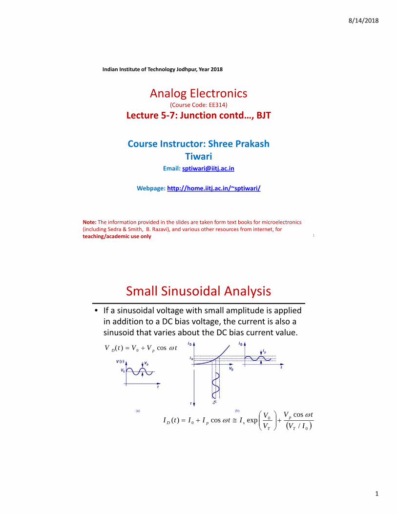
small sinusoidal analysis
TRANSCRIPT
8/14/2018
1
Analog Electronics(Course Code: EE314)
Lecture 5‐7: Junction contd…, BJT
Indian Institute of Technology Jodhpur, Year 2018
Course Instructor: Shree PrakashTiwari
Email: [email protected]
Webpage: http://home.iitj.ac.in/~sptiwari/
1
Note: The information provided in the slides are taken form text books for microelectronics (including Sedra & Smith, B. Razavi), and various other resources from internet, for teaching/academic use only
Small Sinusoidal Analysis• If a sinusoidal voltage with small amplitude is applied in addition to a DC bias voltage, the current is also a sinusoid that varies about the DC bias current valuesinusoid that varies about the DC bias current value.
tVVtV pD cos)( 0
0
00 /
cosexpcos)(
IV
tV
V
VItIItI
T
p
TspD
8/14/2018
2
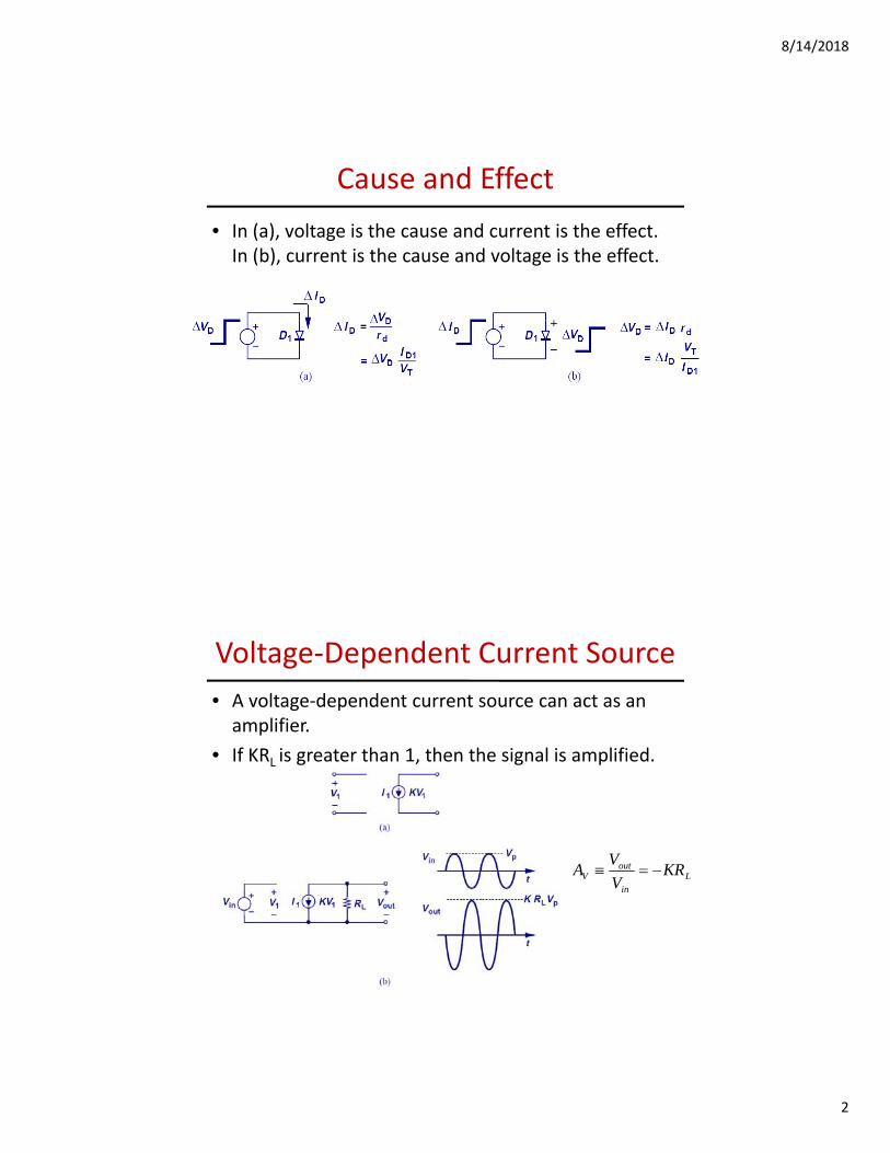
Cause and Effect
• In (a), voltage is the cause and current is the effect. In (b), current is the cause and voltage is the effect.
Voltage‐Dependent Current Source
• A voltage‐dependent current source can act as an amplifier.
• If KRL is greater than 1, then the signal is amplified.
Lout
V KRV
VA
inV
8/14/2018
3
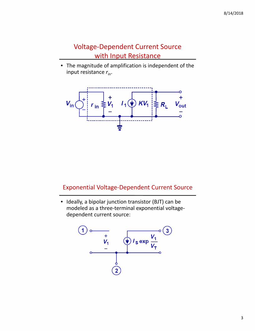
Voltage‐Dependent Current Source with Input Resistance
• The magnitude of amplification is independent of the input resistance rin.
Exponential Voltage‐Dependent Current Source
• Ideally, a bipolar junction transistor (BJT) can be modeled as a three‐terminal exponential voltage‐dependent current source:dependent current source:
8/14/2018
4
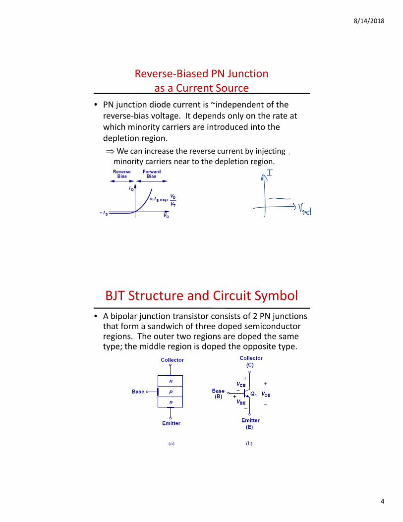
Reverse‐Biased PN Junction as a Current Source
• PN junction diode current is ~independent of the reverse‐bias voltage. It depends only on the rate at h h d d hwhich minority carriers are introduced into the
depletion region.
We can increase the reverse current by injecting minority carriers near to the depletion region.
BJT Structure and Circuit Symbol
• A bipolar junction transistor consists of 2 PN junctions that form a sandwich of three doped semiconductor regions. The outer two regions are doped the sameregions. The outer two regions are doped the same type; the middle region is doped the opposite type.
8/14/2018
5
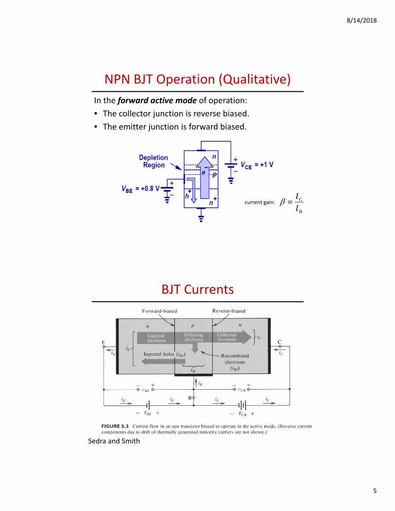
NPN BJT Operation (Qualitative)
In the forward active mode of operation:
• The collector junction is reverse biased.
• The emitter junction is forward biased.
B
C
I
Icurrent gain:
BJT Currents
Sedra and Smith

8/14/2018
6
Base Current
• The base current consists of two components:
1) Injection of holes into the emitter, and
2) Recombination of holes with electrons injected from the emitter.
BC II
BJT Design
• Important features of a well‐designed BJT (large ):– Injected minority carriers do not recombine in the quasi‐neutral base region.
Make a quasi neutral base width small compared to minority carrier diffusion length, WB 0.1m
– Emitter current is comprised almost entirely of carriers injected into the base (rather than carriers injected into the emitter).
Dope emitter more heavily than base.
8/14/2018
7
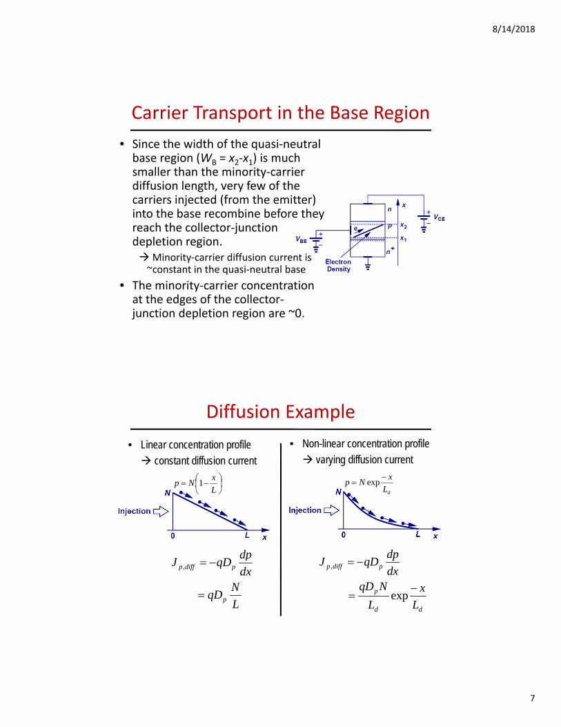
Carrier Transport in the Base Region
• Since the width of the quasi‐neutral base region (WB = x2‐x1) is much smaller than the minority carriersmaller than the minority‐carrier diffusion length, very few of the carriers injected (from the emitter) into the base recombine before they reach the collector‐junction depletion region.Minority carrier diffusion current isMinority‐carrier diffusion current is ~constant in the quasi‐neutral base
• The minority‐carrier concentration at the edges of the collector‐junction depletion region are ~0.
Diffusion Example
• Non-linear concentration profile
varying diffusion current• Linear concentration profile
constant diffusion current
dp dp
dL
xNp
exp
L
xNp 1
L
NqD
dx
dpqDJ
p
pdiffp
,
dd
p
pdiffp
L
x
L
NqDdx
dpqDJ
exp
,
8/14/2018
8
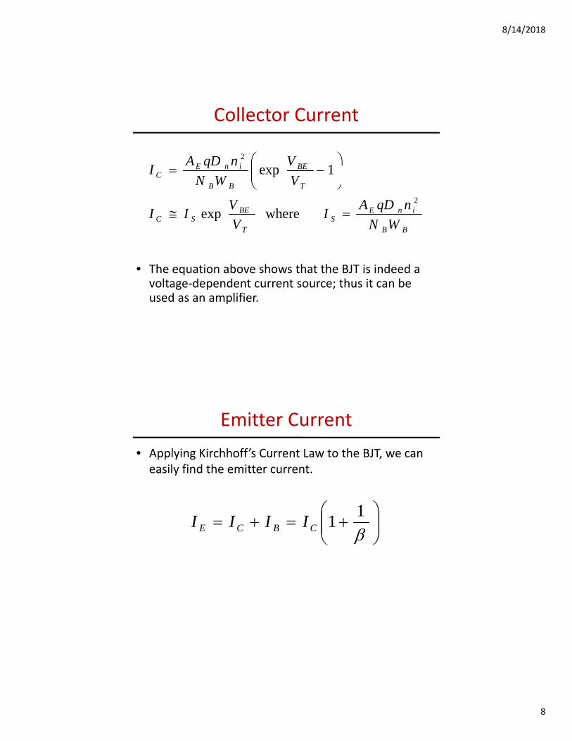
Collector Current
BEinEC
VnqDAI
2
1exp
BB
inES
T
BESC
TBBC
WN
nqDAI
V
VII
VWN2
whereexp
p
• The equation above shows that the BJT is indeed a voltage‐dependent current source; thus it can be used as an amplifier.
Emitter Current
• Applying Kirchhoff’s Current Law to the BJT, we can easily find the emitter current.
1
1CBCE IIII
8/14/2018
9
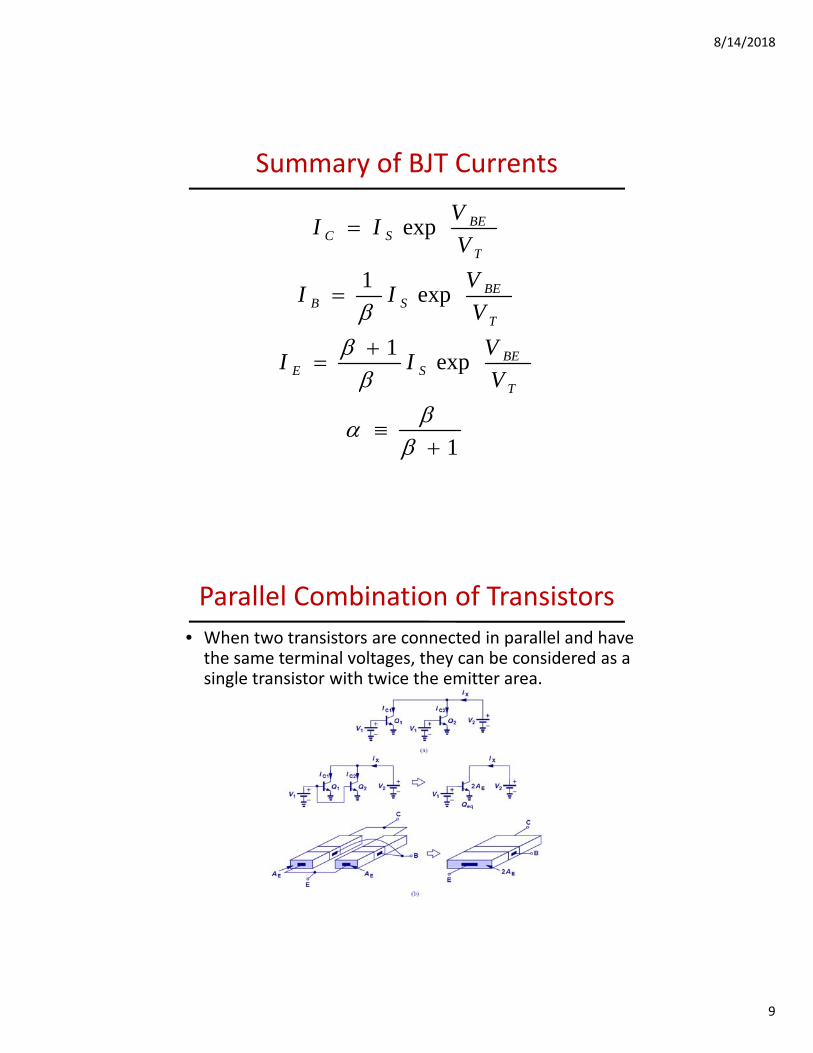
Summary of BJT Currents
exp BESC V
VII
exp1
exp1
BESE
T
BESB
T
VII
V
VII
V
1
p
TSE V
Parallel Combination of Transistors
• When two transistors are connected in parallel and have the same terminal voltages, they can be considered as a single transistor with twice the emitter area.single transistor with twice the emitter area.
8/14/2018
10
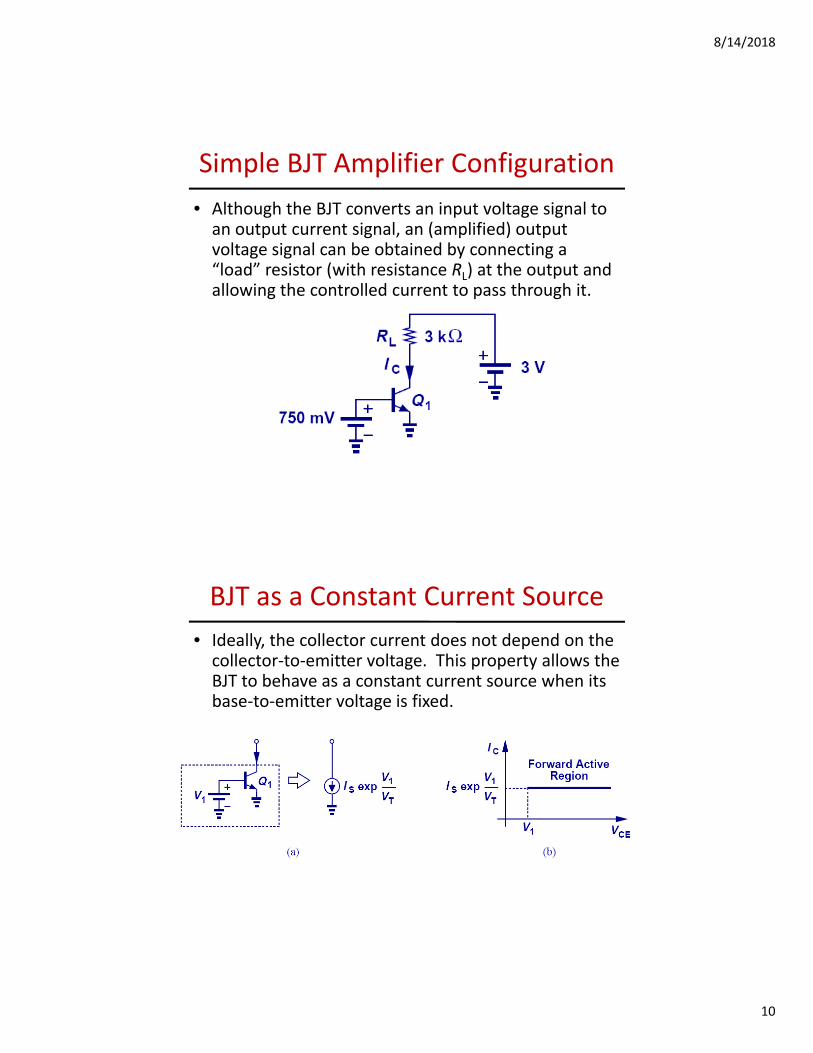
Simple BJT Amplifier Configuration
• Although the BJT converts an input voltage signal to an output current signal, an (amplified) output voltage signal can be obtained by connecting avoltage signal can be obtained by connecting a “load” resistor (with resistance RL) at the output and allowing the controlled current to pass through it.
BJT as a Constant Current Source
• Ideally, the collector current does not depend on the collector‐to‐emitter voltage. This property allows the BJT to behave as a constant current source when itsBJT to behave as a constant current source when its base‐to‐emitter voltage is fixed.
8/14/2018
11
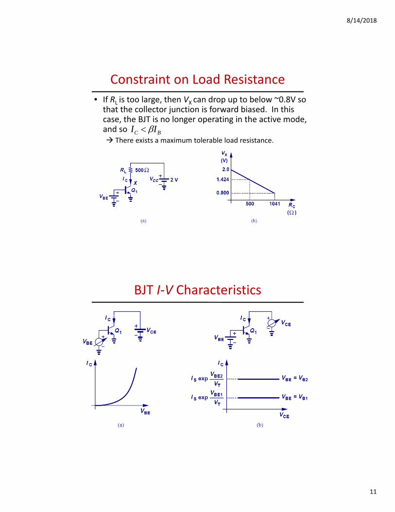
Constraint on Load Resistance
• If RL is too large, then VX can drop up to below ~0.8V so that the collector junction is forward biased. In this case, the BJT is no longer operating in the active mode,case, the BJT is no longer operating in the active mode, and so There exists a maximum tolerable load resistance.
BC II
BJT I‐V Characteristics
8/14/2018
12
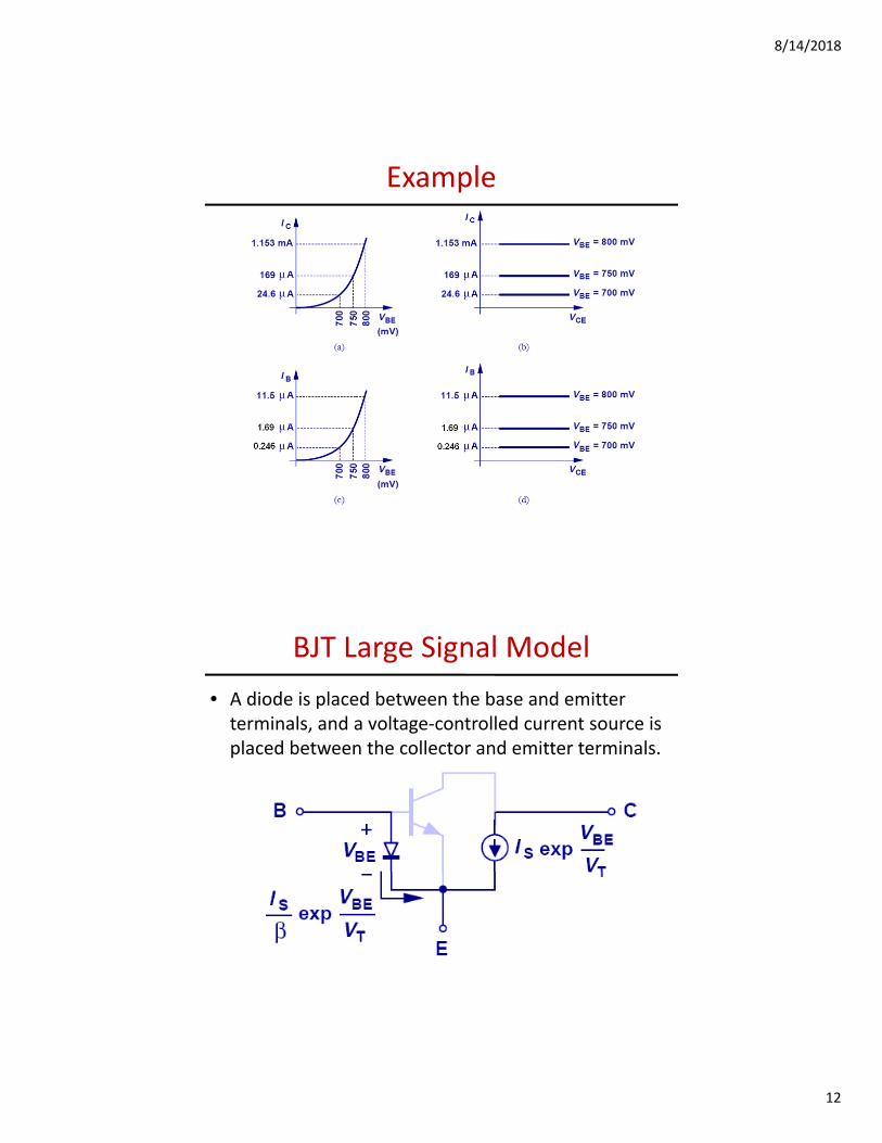
Example
BJT Large Signal Model
• A diode is placed between the base and emitter terminals, and a voltage‐controlled current source is l d b h ll d lplaced between the collector and emitter terminals.
8/14/2018
13
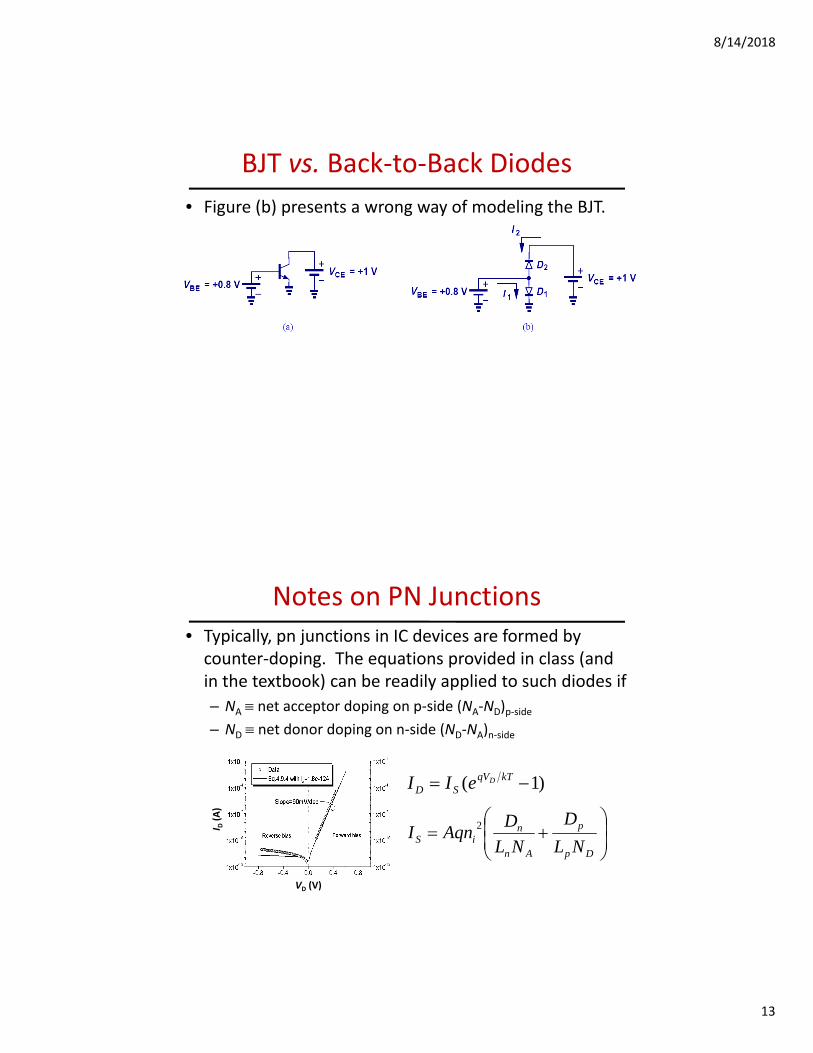
BJT vs. Back‐to‐Back Diodes
• Figure (b) presents a wrong way of modeling the BJT.
Notes on PN Junctions• Typically, pn junctions in IC devices are formed by counter‐doping. The equations provided in class (and in the textbook) can be readily applied to such diodes ifin the textbook) can be readily applied to such diodes if
– NA net acceptor doping on p‐side (NA‐ND)p‐side– ND net donor doping on n‐side (ND‐NA)n‐side
)1( kTVqSD
DeII
Dp
p
An
niS NL
D
NL
DAqnI 2
VD (V)
I D(A)
8/14/2018
14
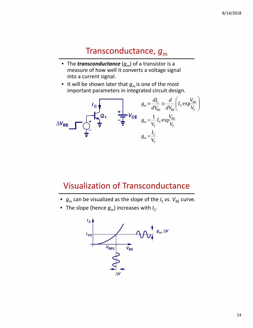
Transconductance, gm• The transconductance (gm) of a transistor is a measure of how well it converts a voltage signal into a current signal.into a current signal.
• It will be shown later that gm is one of the most important parameters in integrated circuit design.
T
BES
BEBE
Cm
V
V
VI
dV
d
dV
dIg
1
exp
T
Cm
T
BES
Tm
V
Ig
V
VI
Vg
exp1
Visualization of Transconductance
• gm can be visualized as the slope of the IC vs. VBE curve.
• The slope (hence gm) increases with IC.
8/14/2018
15
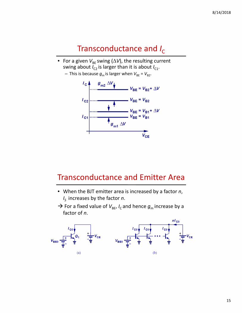
Transconductance and IC • For a given VBE swing (V), the resulting current swing about IC2 is larger than it is about IC1. – This is because g is larger when V = V– This is because gm is larger when VBE = VB2.
Transconductance and Emitter Area
• When the BJT emitter area is increased by a factor n, IS increases by the factor n.
For a fixed value of VBE, IC and hence gm increase by a factor of n.
8/14/2018
16
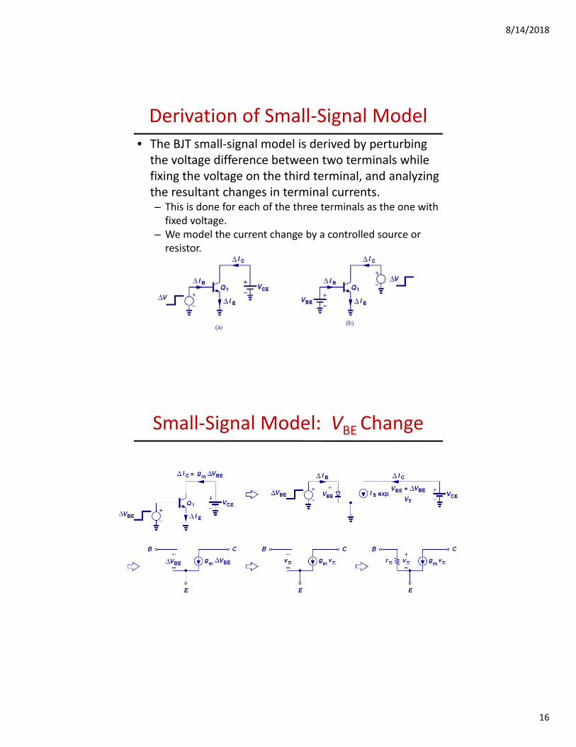
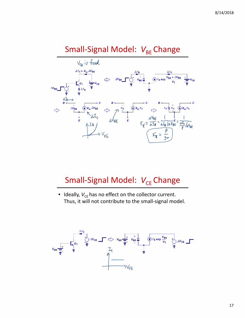
Derivation of Small‐Signal Model• The BJT small‐signal model is derived by perturbing the voltage difference between two terminals while fixing the voltage on the third terminal and analyzingfixing the voltage on the third terminal, and analyzing the resultant changes in terminal currents. – This is done for each of the three terminals as the one with fixed voltage.
– We model the current change by a controlled source or resistor.
Small‐Signal Model: VBE Change
8/14/2018
17
Small‐Signal Model: VBE Change
Small‐Signal Model: VCE Change
• Ideally, VCE has no effect on the collector current. Thus, it will not contribute to the small‐signal model.
8/14/2018
18
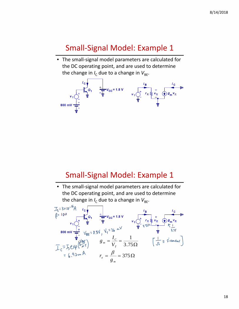
Small‐Signal Model: Example 1• The small‐signal model parameters are calculated for the DC operating point, and are used to determine the change in I due to a change in Vthe change in IC due to a change in VBE.
Small‐Signal Model: Example 1• The small‐signal model parameters are calculated for the DC operating point, and are used to determine the change in I due to a change in Vthe change in IC due to a change in VBE.
1I
375
75.31
m
T
Cm
gr
VI
g
8/14/2018
19
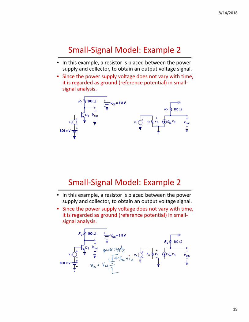
Small‐Signal Model: Example 2
• In this example, a resistor is placed between the power supply and collector, to obtain an output voltage signal.
• Since the power supply voltage does not vary with time• Since the power supply voltage does not vary with time, it is regarded as ground (reference potential) in small‐signal analysis.
8/14/2018
20
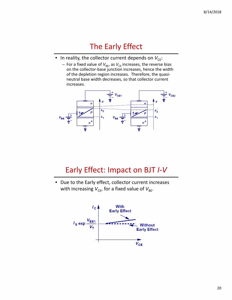
The Early Effect• In reality, the collector current depends on VCE:
– For a fixed value of VBE, as VCE increases, the reverse bias on the collector‐base junction increases, hence the width j ,of the depletion region increases. Therefore, the quasi‐neutral base width decreases, so that collector current increases.
Early Effect: Impact on BJT I‐V
• Due to the Early effect, collector current increases with increasing VCE, for a fixed value of VBE.
8/14/2018
21
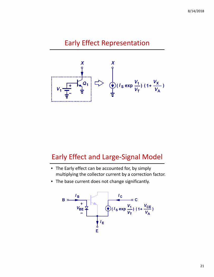
Early Effect Representation
Early Effect and Large‐Signal Model
• The Early effect can be accounted for, by simply multiplying the collector current by a correction factor.
• The base current does not change significantly.
8/14/2018
22
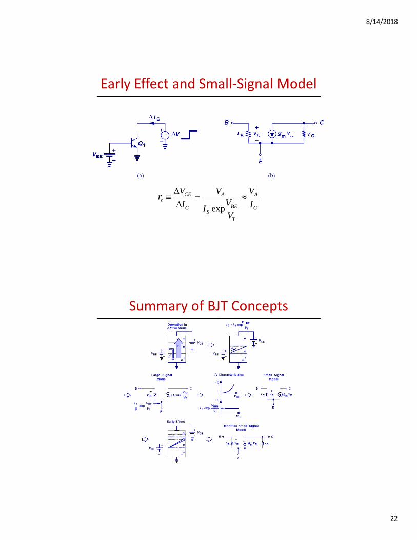
Early Effect and Small‐Signal Model
VVV
C
A
T
BES
A
C
CEo I
V
VV
I
V
I
Vr
exp
Summary of BJT Concepts

8/14/2018
23
What next
• BJT contd….