smarresearch fieldbus communications controller … technologysource asynchronous bus (ready...
TRANSCRIPT

©Smar Research Corporation 1 FB 3050DS-0404
HART®
Fieldbus Profibus Intrinsic Safety Configuration Tools Semiconductors Training Custom Design
SmarResearch TechnologySource
Asynchronous Bus (READY Methodology) Features • Built-in Manchester encoder/decoder • Built-in two channel DMA controller • Automatic polarity detection and correction • Automatic receiver frame check sequence (FCS) detection • Software controlled transmitter FCS generation • Automatic message type and address recognition • 31.25K and 1Mbit/sec. data rates • Transmitter jabber inhibit circuitry • Available in a 100-pin TQFP package • Maskable multisource Interrupt Structures reduce software response
times • CMOS low power consumption and standby mode • TIMERS available for data link layer timing • Conforms to the ISA SP50 .02 1992 Part 2, Foundation Fieldbus
Physical Layer Definition • Compatible with all popular microprocessors and microcontrollers • Compatible with Motorola and Intel buses
Fieldbus Communications Controller
FB3050 DataSheet
Visit the SmarResearch technology center at: www.smarresearch.com

©Smar Research Corporation 2 FB 3050DS-0404
General Description The FB3050 Fieldbus Interface and
Controller conforms to the IEC 1158-2 standard, Fieldbus Physical Layer Definition. It provides a high level Master or Slave Fieldbus interface with both embedded and host microprocessors.
The FB3050 contains Manchester
data encoders and decoders on chip and uses a medium interface plus external filters to connect to a Fieldbus system. It automatically detects and corrects polarity reversals on improperly wired connections. The Controller automatically checks the Frame Check Sequence (FCS) for received data packets and generates them for transmitted data packets when enabled by a software control command. Frame status is available by reading the internal status registers. A Jabber Inhibit function helps assure a transmitter does not disable the communications network by transmitting beyond a specified time.
An on-chip two channel Direct
Memory Access (DMA) circuit is incorporated for high throughput. Once the DMA is configured, data blocks (frames, buffers) can be sent and received to and from the system memory without significant byte transfer overhead. When interfacing with Intel or generic type processors the DMA uses the READY signal to force the microprocessor into wait status until the DMA access cycle has finished.
Complete control and status
information is available through internal registers. These registers are easily read or written to configure and operate the FB3050 Controller. To facilitate interfacing with various host controllers, two clock sources are used; one for system synchronization and a second for data rate control.
To reduce software overhead, the FB3050 Controller provides detection of the Frame Control character. Depending on the value received, an equality test for 8 bit, 16 bit or 32 bit addresses is made by comparing the received address with a table of addresses contained in memory. The search for a match is automatic. An interrupt is generated when a match occurs. Only one address loads into an internal register for an 8 bit compare. Address fields in memory support a variable number of 16 bit and 32 bit addresses. Frame Control message types that do not require address recognition are also detected and can generate an interrupt.
The FB3050 has a flexible interrupt structure. A single interrupt will cause the host to read internal status registers to determine the source. All interrupt sources are maskable and identifiable. An interrupt is generated by a number of conditions or by any of the controllers’ three timers. The Timer Module provides octet, 1/32 millisecond and millisecond timing references. All of these conditions are also maskable.
FB
30
50
Ge
ne
ral D
esc
rip
tio
n

©Smar Research Corporation 3 FB 3050DS-0404
Figure 1 - Pin Configuration
Pin Configuration
FB
30
50
- P
in C
on
fig
ura
tio
n
SMARFB 3050 TQ
6562 0369746YVG
GND
PO_SOH
PO_MADDR_9
PO_MADDR_8
PO_MADDR_7
PO_MADDR_6
PO_MADDR_5
PO_MADDR_4
1
2
3
4
5
6
7
8
9
10
11
12
13
14
15
16
17
18
19
20
21
22
23
24
25
26 27 28 29 30 31 32 33 34 35 36 37 38 39 40 41 42 43 44 45 46 47 48 49 50
75
74
73
72
71
70
69
68
67
66
65
64
63
62
61
60
59
58
57
56
55
54
53
52
51
100 99 98 97 96 95 94 93 92 91 90 89 88 87 86 85 84 83 82 81 80 79 78 77 76
PO_MADDR_2
PO_MADDR_3
PO_EOH
VCC
PO_MADDR_1
PO_SYN
GND
PB_MDATA_2
PB_MDATA_4
PO_MADDR_0
PB_MDATA_0
PB_MDATA_3
PI_ADDR_14
GND
PO_READY
PO_INT_I
PI_RESET_I
PI_ADDR_15
PB_CDATA_7
PB_CDATA_6
PI_ADDR_13
PB_CDATA_5
PI_ADDR_12
PB_CDATA_4
PB_CDATA_2
PI_ADDR_11
PB_CDATA_3
PI_ADDR_10
PI_ADDR_9
PB_CDATA_1
PI_ADDR_8
PB_CDATA_0
PI_CLOCK
WR/
RD/
PI_CAS
VCC
PO_X
ADD
R_6
GN
D
PO_X
ADD
R_0
PO_X
ADD
R_1
PO_X
ADD
R_2
PO_X
ADD
R_3
PO_X
ADD
R_4
PO_X
ADD
R_5
PO_X
ADD
R_7
PI_A
DD
R_0
PI_A
DD
R_1
PI_A
DD
R_2
GN
D
PI_A
DD
R_3
PI_A
DD
R_4
PI_A
DD
R_5
PI_A
DD
R_6
PI_A
DD
R_7
PO_M
ADD
R_1
5
PO_M
ADD
R_1
4
PO_M
ADD
R_1
3
PO_M
ADD
R_1
2
PO_M
ADD
R_1
1
PO_M
ADD
R_1
0
VCC
PB_MDATA_1
PB_MDATA_5
PO_TDRE
PO_RDRF
VCC
GN
D
PB_M
DAT
A_6
PB_M
DAT
A_7
PI_P
HPD
U
PO_T
ACT
PO_P
HPD
U
PO_M
CSO
PO_M
CSD
_I
PO_M
CSF
_I
PO_M
CSE
_I
PI_C
SREG
_I
PI_C
SMEM
_I
PO_M
RO
M_I
PO_M
OE
PI_M
OD
E
PI_M
UX_
ON
PI_C
LK12
5
PO_M
RAM
_I
PO_M
WR
PI_E
DG
E
PI_I
NT_
I
N/C
GN
D
PI_N
ETC
LOC
K
VCC
©Smar Research Corporation 4 FB 3050DS-0404
Pin Descriptions
The FB3050’s pins are divided into four major groups: Memory Interface, Microprocessor Interface, Fieldbus Interface, and Clocks & Timing Interface.
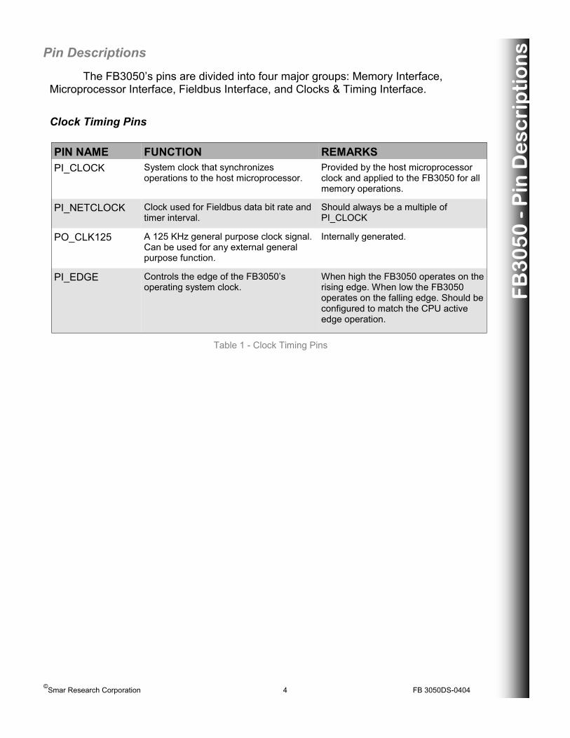
PIN NAME FUNCTION REMARKS PI_CLOCK System clock that synchronizes
operations to the host microprocessor. Provided by the host microprocessor clock and applied to the FB3050 for all memory operations.
PI_NETCLOCK Clock used for Fieldbus data bit rate and timer interval.
Should always be a multiple of PI_CLOCK
PO_CLK125 A 125 KHz general purpose clock signal. Can be used for any external general purpose function.
Internally generated.
PI_EDGE Controls the edge of the FB3050’s operating system clock.
When high the FB3050 operates on the rising edge. When low the FB3050 operates on the falling edge. Should be configured to match the CPU active edge operation.
Clock Timing Pins
Table 1 - Clock Timing Pins
FB
30
50
- P
in D
esc
rip
tio
ns

©Smar Research Corporation 5 FB 3050DS-0404
Pin Descriptions
Microprocessor Interface Pins
Table 2 - Microprocessor Interface Pins
PIN NAME FUNCTION REMARKS PI_ADDR[15:0] Controller address bus from the
microprocessor to the FB3050. When using a multiplexed address bus, the PI_ADDR[7:0] pins should be connected to GND.
PB_CDATA[7:0] Controller data bus from the microprocessor to the FB3050.
PI_CSMEM_I An active low signal enabling the addressing low 32Kbytes of memory through the FB3050.
PI_CSREG_I An active low signal used to enable the location of the internal registers.
PI_RESET_I An active low signal that forces the FB3050 into an initialized state.
Originates from a reset chain controlled by the microprocessor or can be generated by a resistor-capacitor circuit. Signal should be equal to or greater than 200 nsec.
WR/ WRITE control signal from the microprocessor.
RD/ READ control signal from the microprocessor.
PI_CAS Address strobe signal from the microprocessor when the memory address is multiplexed from the data bus.
This signal should be held at VCC when not in the multiplexed address mode.
PI_MUXON Selects the multiplexed address mode when high.
PI_MODE Defines the type of microprocessor interfaced to the FB3050.
High for an asynchronous bus microprocessor (Intel or generic).
PO_READY Used with a microprocessor that can be put into an open collector output.
Synchronizes the DMA cycle with the computer memory access, or speed matches a fast microprocessor with the FB3050.
PI_INT_I An active low signal that receives an interrupt from an external device.
If not used connect to high.
PO_INT_I An active low signal that indicates an enabled interrupt source.
FB
30
50
- P
in D
esc
rip
tio
ns
©Smar Research Corporation 6 FB 3050DS-0404
Pin Descriptions
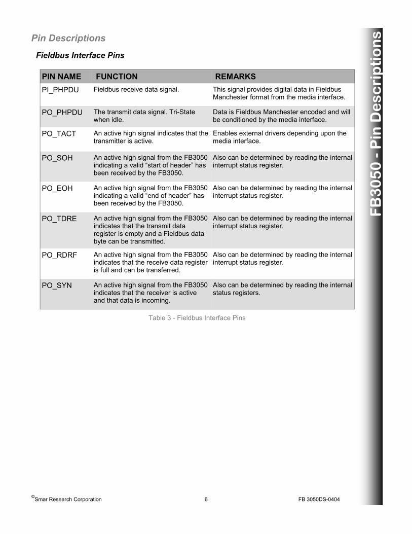
Fieldbus Interface Pins
Table 3 - Fieldbus Interface Pins
PIN NAME FUNCTION REMARKS PI_PHPDU Fieldbus receive data signal. This signal provides digital data in Fieldbus
Manchester format from the media interface.
PO_PHPDU The transmit data signal. Tri-State when idle.
Data is Fieldbus Manchester encoded and will be conditioned by the media interface.
PO_TACT An active high signal indicates that the transmitter is active.
Enables external drivers depending upon the media interface.
PO_SOH An active high signal from the FB3050 indicating a valid “start of header” has been received by the FB3050.
Also can be determined by reading the internal interrupt status register.
PO_EOH An active high signal from the FB3050 indicating a valid “end of header” has been received by the FB3050.
Also can be determined by reading the internal interrupt status register.
PO_TDRE An active high signal from the FB3050 indicates that the transmit data register is empty and a Fieldbus data byte can be transmitted.
Also can be determined by reading the internal interrupt status register.
PO_RDRF An active high signal from the FB3050 indicates that the receive data register is full and can be transferred.
Also can be determined by reading the internal interrupt status register.
PO_SYN An active high signal from the FB3050 indicates that the receiver is active and that data is incoming.
Also can be determined by reading the internal status registers.
FB
30
50
- P
in D
esc
rip
tio
ns
©Smar Research Corporation 7 FB 3050DS-0404
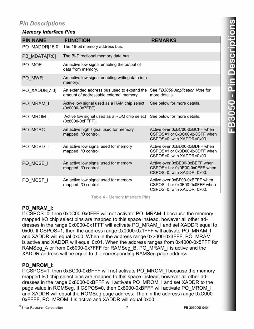
Pin Descriptions Memory Interface Pins
PIN NAME FUNCTION REMARKS PO_MADDR[15:0] The 16-bit memory address bus.
PB_MDATA[7:0] The Bi-Directional memory data bus.
PO_MOE An active low signal enabling the output of data from memory.
PO_MWR An active low signal enabling writing data into memory.
PO_XADDR[7:0] An extended address bus used to expand the amount of addressable external memory
See FB3050 Application Note for more details.
PO_MRAM_I Active low signal used as a RAM chip select (0x0000-0x7FFF).
See below for more details.
PO_MROM_I Active low signal used as a ROM chip select (0x8000-0xFFFF).
See below for more details.
PO_MCSC An active high signal used for memory mapped I/O control.
Active over 0xBC00-0xBCFF when CSPOS=1 or 0x0C00-0x0CFF when CSPOS=0, with XADDR=0x00.
PO_MCSD_I An active low signal used for memory mapped I/O control.
Active over 0xBD00-0xBDFF when CSPOS=1 or 0x0D00-0x0DFF when CSPOS=0, with XADDR=0x00.
PO_MCSE_I An active low signal used for memory mapped I/O control.
Active over 0xBE00-0xBEFF when CSPOS=1 or 0x0E00-0x0EFF when CSPOS=0, with XADDR=0x00.
PO_MCSF_I An active low signal used for memory mapped I/O control.
Active over 0xBF00-0xBFFF when CSPOS=1 or 0x0F00-0x0FFF when CSPOS=0, with XADDR=0x00.
Table 4 - Memory Interface Pins
FB
30
50
- P
in D
esc
rip
tio
ns
PO_MRAM_I: If CSPOS=0, then 0x0C00-0x0FFF will not activate PO_MRAM_I because the memory mapped I/O chip select pins are mapped to this space instead, however all other ad-dresses in the range 0x0000-0x1FFF will activate PO_MRAM_I and set XADDR equal to 0x00. If CSPOS=1, then the address range 0x0000-0x1FFF will activate PO_MRAM_I and XADDR will equal 0x00. When in the address range 0x2000-0x3FFF, PO_MRAM_I is active and XADDR will equal 0x01. When the address ranges from 0x4000-0x5FFF for RAMSeg_A or from 0x6000-0x7FFF for RAMSeg_B, PO_MRAM_I is active and the XADDR address will be equal to the corresponding RAMSeg page address. PO_MROM_I: If CSPOS=1, then 0xBC00-0xBFFF will not activate PO_MROM_I because the memory mapped I/O chip select pins are mapped to this space instead, however all other ad-dresses in the range 0x8000-0xBFFF will activate PO_MROM_I and set XADDR to the page value in ROMSeg. If CSPOS=0, then 0x8000-0xBFFF will activate PO_MROM_I and XADDR will equal the ROMSeg page address. Then in the address range 0xC000-0xFFFF, PO_MROM_I is active and XADDR will equal 0x00.

©Smar Research Corporation 8 FB 3050DS-0404
Pin Descriptions
Pin Summary
PIN# NAME TYPE PIN# NAME TYPE 1 GND Power 26 GND Power
2 PO_SOH Output 27 PB_MDATA_6 Bi-Directional
3 PO_MADDR_9 Output 28 PB_MDATA_7 Bi-Directional
4 PO_MADDR_8 Output 29 PI_PHPDU Input
5 PO_MADDR_7 Output 30 PO_TACT Output
6 PO_MADDR_6 Output 31 PO_PHPDU Output
7 PO_MADDR_5 Output 32 PO_MCSC Not Used
8 PO_MADDR_4 Output 33 PO_MCSD_I Not Used
9 PO_MADDR_3 Output 34 PO_MCSE_I Not Used
10 PO_MADDR_2 Output 35 PO_MCSF_I Not Used
11 PO_EOH Output 36 PI_CSREG_I Input
12 VCC Power 37 PI_CSMEM_I Input
13 GND Power 38 PI_MODE Input
14 PO_SYN Output 39 PO_MOE Output
15 PO_MADDR_1 Output 40 PO_MROM_I Not Used
16 PO_MADDR_0 Output 41 PO_MRAM_I Output
17 PB_MDATA_0 Bi-Directional 42 PO_MWR Output
18 PB_MDATA_1 Bi-Directional 43 PI_INT_I Input
19 PB_MDATA_2 Bi-Directional 44 PI_MUX_ON Input
20 PB_MDATA_3 Bi-Directional 45 PI_EDGE Input
21 PB_MDATA_4 Bi-Directional 46 PO_CLK125 Output
22 PB_MDATA_5 Bi-Directional 47 N/C N/C
23 PO_TDRE Output 48 GND Power
24 PO_RDRF Output 49 PI_NETCLOCK Input
25 VCC Power 50 VCC Power
Table 5a - Pin Summary F
B3
05
0 -
Pin
De
scri
pti
on
s

©Smar Research Corporation 9 FB 3050DS-0404
Pin Descriptions
Pin Summary
Table 5b - Pin Summary
PIN# NAME TYPE PIN# NAME TYPE 51 GND Power 76 GND Power
52 PO_READY Output 77 PO_XADDR_0 Output
53 PO_INT_I Output 78 PO_XADDR_1 Output
54 PI_RESET_I Input 79 PO_XADDR_2 Output
55 PI_ADDR_15 Input 80 PO_XADDR_3 Output
56 PB_CDATA_7 Bi-Directional 81 PO_XADDR_4 Output
57 PI_ADDR_14 Input 82 PO_XADDR_5 Output
58 PB_CDATA_6 Bi-Directional 83 PO_XADDR_6 Output
59 PI_ADDR_13 Input 84 PO_XADDR_7 Output
60 PB_CDATA_5 Bi-Directional 85 PI_ADDR_0 Input
61 PI_ADDR_12 Input 86 PI_ADDR_1 Input
62 PB_CDATA_4 Bi-Directional 87 PI_ADDR_2 Input
63 PI_ADDR_11 Input 88 GND Power
64 PB_CDATA_3 Bi-Directional 89 PI_ADDR_3 Input
65 PI_ADDR_10 Input 90 PI_ADDR_4 Input
66 PB_CDATA_2 Bi-Directional 91 PI_ADDR_5 Input
67 PI_ADDR_9 Input 92 PI_ADDR_6 Input
68 PB_CDATA_1 Bi-Directional 93 PI_ADDR_7 Input
69 PI_ADDR_8 Input 94 PO_MADDR_15 Output
70 PB_CDATA_0 Bi-Directional 95 PO_MADDR_14 Output
71 PI_CLOCK Input 96 PO_MADDR_13 Output
72 WR/ Input 97 PO_MADDR_12 Output
73 RD/ Input 98 PO_MADDR_11 Output
74 PI_CAS Input 99 PO_MADDR_10 Output
75 VCC Power 100 VCC Power F
B3
05
0 -
Pin
De
scri
pti
on
s

©Smar Research Corporation 10 FB 3050DS-0404
Memory Mapping The CPU can access up to 32KB of RAM and 32KB of ROM via the PO_MRAM_I
and PO_MROM_I pins respectively. To access more than 64KB of memory, the extended addressing of the FB3050 can be used or additional flash and SRAM can be connected directly to the CPU without passing through the FB3050.
Whenever PI_CSREG_I is driven active low, the internal registers of the FB3050
will appear every 8KB over the entire address space. This can be seen in Figure 2, Diagram C below. In addition, the memory spaces that correspond to the FB3050 chip selects are also mapped to the internal registers of the FB3050. In this way, for CPU’s that do not include chip selects, one of the FB3050 chip selects can be tied directly to PI_CSREG_I to access the FB3050 internal registers. For CPU’s that include chip selects, the FB3050 internal registers can be mapped to any 8KB address space. The CSPOS bit of FB_CNTRL_0 determines the address location of the FB3050 chip selects. The effects of CSPOS can be seen in Diagrams A and B below. For more information on memory interfacing, extended addressing and chip selects, please refer to the FB3050 Application Note.
FB
30
50
- M
em
ory
Ma
pp
ing
FB3050 Internal Reg.
FB3050 Internal Reg.
FB3050 Internal Reg.
FB3050 Internal Reg.
FB3050 Internal Reg.
FB3050 Internal Reg.
FB3050 Internal Reg.
FB3050 Internal Reg.
FB3050 Internal Reg.
64K
Add
ress
Spa
ce
FFFF
0000007F
2000
4000
6000
8000
A000
C000
E000
PI_CSREG_I = 0
PO_MCSF_IPO_MCSE_IPO_MCSD_IPO_MCSC_I
0FFF0F00
0E00
0D00
0C00
CSPOS=0FB3050 Internal Reg.
0C00
0FFF
PO_MCSF_IPO_MCSE_IPO_MCSD_IPO_MCSC_I
BFFFBF00
BE00
BD00
BC00
BC00
BFFF CSPOS=1
*Drawing not to scale
207F
407F
607F
807F
A07F
C07F
E07F
FFFF
0000
8000
0C00
1000
BC00
BFFF
*Drawing not to scale
PO_MCSF_IPO_MCSE_IPO_MCSD_IPO_MCSC_I
0D00
0E00
0F00
FFFF
0000
8000
BC00
C000
BFFF
*Drawing not to scale
PO_MCSF_IPO_MCSE_IPO_MCSD_IPO_MCSC_I
BE00
BF00
CSPOS = 1PI_CSREG_I = 1
CSPOS = 0PI_CSREG_I = 1
xx7F
xx3F
xx00
each contains
xx40
Shadow ofRegisters
xx00 - xx3F
FB3050 InternalRegisters
Diagram A Diagram B Diagram C
Figure 2 - Pin Configuration

©Smar Research Corporation 11 FB 3050DS-0404
Interface To General CPU A host bus for code and/or data can be used with the FB3050 when interfaced to a general CPU. A separate SRAM should be used when working with frames used to perform functions such as storing received frames, reading frames to be transmitted, and looking for an address match in address tables. The ready signal can be used to extend the memory access when interfacing with a CPU if that CPU provides this function. The FB3050 can be interfaced using two different methods, multiplexed and non-multiplexed. A generic multiplexed environment can be seen in Figure 3, while a non-multiplexed environment can be seen in Figure 4. Refer to the FB3050 Application Notes for more information on CPU and memory interfacing.
Figure 3 - Multiplexed CPU Interface
FB
30
50
- In
terf
ac
e E
nvi
ron
me
nt
CPU RAM
Multiplexed Host BUS
FB3050
CLOCK
MAUPO_PHPDUPI_PHPDU
PO_TXENFIELDBUS
LINE
FB30
50 B
US
ROM
PI_RESET_IPO_INT_I
WR/
RD/
PI_CAS
PI_CLK
XTAL
IRQ/RST/
R/W
E
AS/
Multiplexed Environment
©Smar Research Corporation 12 FB 3050DS-0404
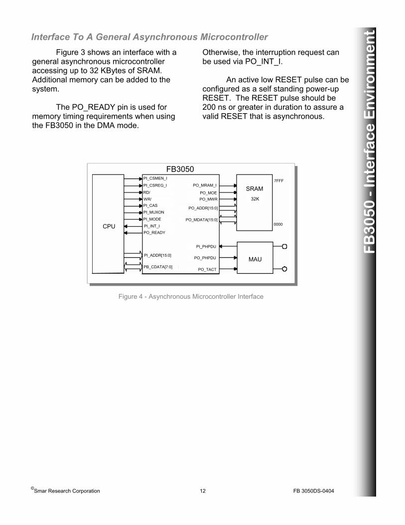
Figure 3 shows an interface with a general asynchronous microcontroller accessing up to 32 KBytes of SRAM. Additional memory can be added to the system. The PO_READY pin is used for memory timing requirements when using the FB3050 in the DMA mode.
Otherwise, the interruption request can be used via PO_INT_I. An active low RESET pulse can be configured as a self standing power-up RESET. The RESET pulse should be 200 ns or greater in duration to assure a valid RESET that is asynchronous.
Interface To A General Asynchronous Microcontroller
Figure 4 - Asynchronous Microcontroller Interface
CPU
MAU
SRAM 32K
PI_CSMEN_I
PI_CSREG_I
RD/
PB_CDATA[7:0]
PI_CAS WR/
PI_MUXON
PI_MODE
PI_INT_I PO_READY
PI_ADDR[15:0]
FB3050
PO_MRAM_I
PO_MOE PO_MWR
PO_ADDR[15:0]
PO_MDATA[15:0]
PI_PHPDU
PO_PHPDU
PO_TACT
7FFF
0000
FB
30
50
- In
terf
ac
e E
nvi
ron
me
nt

©Smar Research Corporation 13 FB 3050DS-0404
Address Recognition
Module
DMA
Module
Timer
Module
Fieldbus I/O Control Module
Interrupt Registers Module
Work Registers Module
Sy
stem
I/O
C
ontro
l M
odul
e
FB30
50
Mem
ory
Bus
CPU
Bu
s
Fleidbus Network
MAU
I N T E R N A L
B U S
Figure 5 - FB3050 Internal Block Diagran
Internal Block Diagram
FB
30
50
- In
tern
al B
lock
Dia
gra
m

©Smar Research Corporation 14 FB 3050DS-0404
System I/O Control Module
The System I/O Control Module controls the data flow between microprocessor memory and Fieldbus memory. The CPU data (PB_CDATA) signal and other signals flow from and to the memory and internal registers (see Figure 5). These pins define which FB3050 actions are requested by the CPU. For example, when PI_CSMEM_I is activated, the System I/O Control
Module signals the DMA Module for the CPU to access memory. Following RD/ and WR/, the proper action will be taken and both PO_MOE or PO_MWR and PO_MRAM_I will be set.
Figure 6 - Fieldbus I/O Control Module
SYSTEM I/O CONTROL MODULE
PI_MODE PI_MUXON PI_RESET
PI_CSMEM_I
RD/ WR/
PI_CAS PI_ADDR
PB_CDATA
PD_MRAM_I PD_MADDR PO_MOE PO_MWR PO_MDATA
INTERNAL BUS
FB
30
50
- S
yste
m I/
O C
on
tro
l Mo
du
le
©Smar Research Corporation 15 FB 3050DS-0404
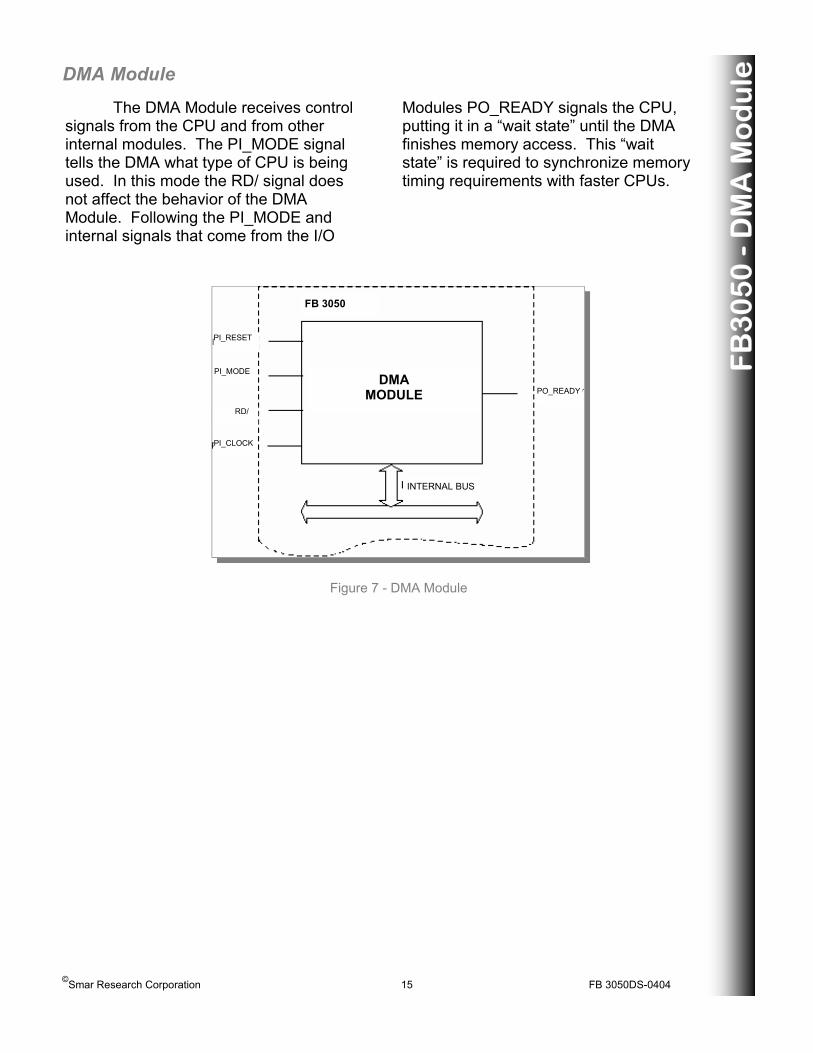
DMA Module
The DMA Module receives control signals from the CPU and from other internal modules. The PI_MODE signal tells the DMA what type of CPU is being used. In this mode the RD/ signal does not affect the behavior of the DMA Module. Following the PI_MODE and internal signals that come from the I/O
Modules PO_READY signals the CPU, putting it in a “wait state” until the DMA finishes memory access. This “wait state” is required to synchronize memory timing requirements with faster CPUs.
Figure 7 - DMA Module
DMA MODULE
INTERNAL BUS
FB 3050
PO_READY
PI_RESET
PI_MODE
RD/
PI_CLOCK
FB
30
50
- D
MA
Mo
du
le

©Smar Research Corporation 16 FB 3050DS-0404
Timer Module
Figure 8 - Timer Module
The Timer Module controls the generation of the internal clocks as well as an external 125 KHz clock for general purposes. The PI_EDGE pin is set for the system to use either a clock’s rising or falling edge. The PI_EDGE pin also
receives two clock signals, PI_CLOCK for system clock synchronization and PI_NETCLOCK for Fieldbus network timing.
FB
30
50
- T
ime
r M
od
ule

©Smar Research Corporation 17 FB 3050DS-0404
Baud Rate and Clock Generator Module
Figure 9 - Baud Rate and Clock Generator Module
The Baud Rate and Clock Generator Module is part of the Timer Module. It selects one of the clock
sources and internal clock configurations based on the FB_CNTRL_2 work register.
MD = “00” - Disable Clock Source MD = “01” - Mode [email protected] MD = “10” - Mode [email protected] MD = “11” - Mode [email protected]
BitTime 16X = Clock Source/Er + 1
[email protected]: WR Only
CLSEL = “0” - Clock Source = F1_CLOCK CLSEL = “1” - Clock Source = F1_NETCLOCK
CLSEL MD1 MD0 BR4 BR3 BR2 BR1 BR0
FB
30
50
- B
au
d R
ate
an
d C
lock
Ge
ne
rato
r M
od
ule
©Smar Research Corporation 18 FB 3050DS-0404
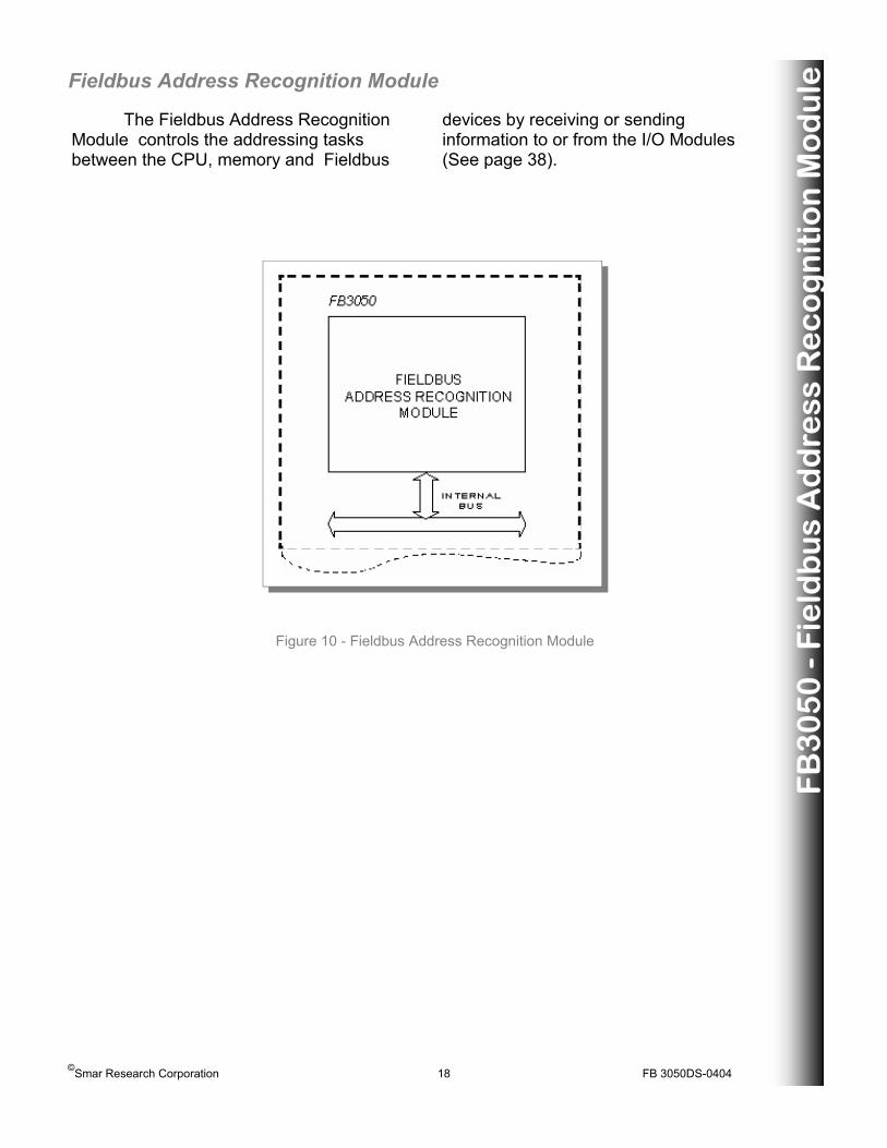
Fieldbus Address Recognition Module
Figure 10 - Fieldbus Address Recognition Module
The Fieldbus Address Recognition Module controls the addressing tasks between the CPU, memory and Fieldbus
devices by receiving or sending information to or from the I/O Modules (See page 38).
FB
30
50
- F
ield
bu
s A
dd
ress
Re
co
gn
itio
n M
od
ule

©Smar Research Corporation 19 FB 3050DS-0404
Fieldbus I/O Control Module
Figure 11 - Fieldbus I/O Control Module
The Fieldbus I/O Control Module controls the data flow between the Fieldbus environment and the system. The DMA and the System I/O send control signals initiating this module to either receive or transmit information.
This module also checks work registers FB_CTRL_0 and FB_CTRL_1 to enable features like transmission/reception using the DMA Mode or the Interruption Request process.
FB
30
50
- F
ield
bu
s I/
O C
on
tro
l Mo
du
le
©Smar Research Corporation 20 FB 3050DS-0404
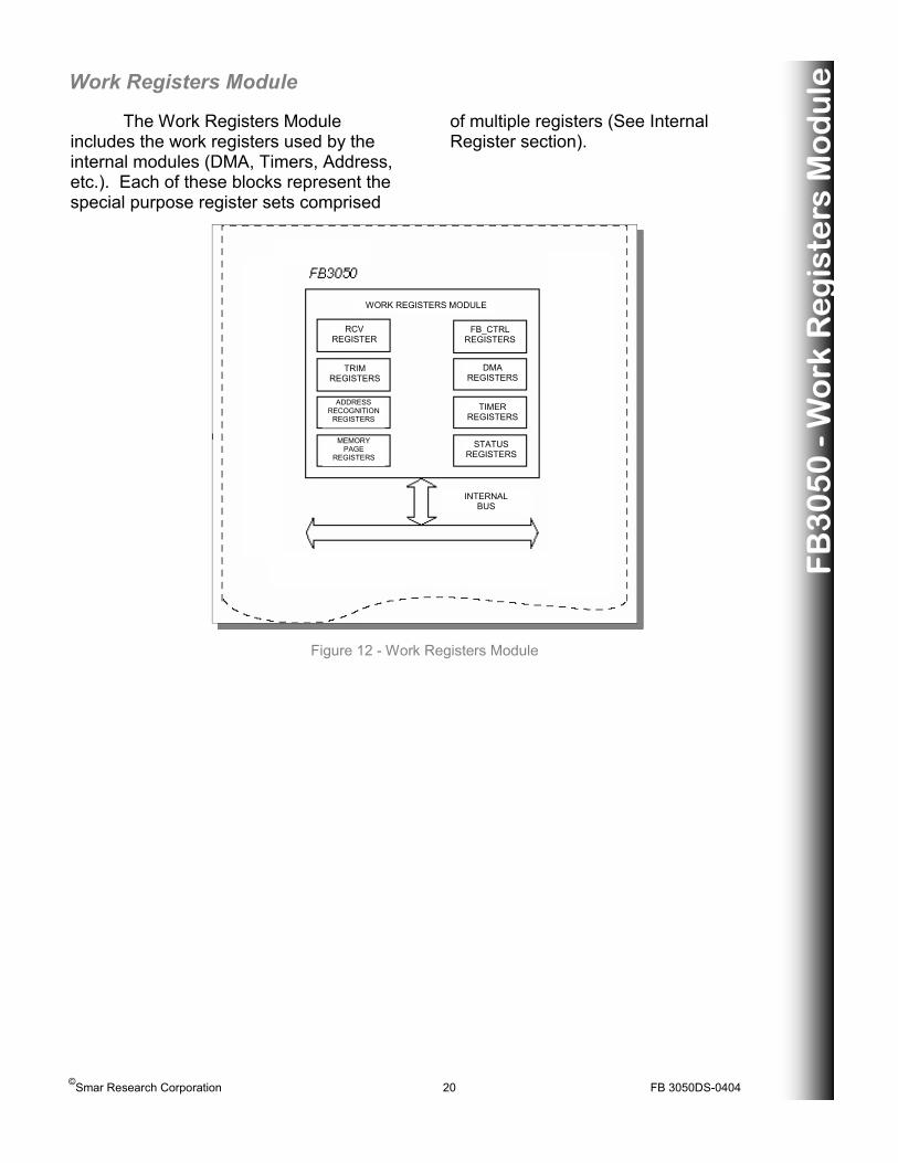
Work Registers Module
Figure 12 - Work Registers Module
The Work Registers Module includes the work registers used by the internal modules (DMA, Timers, Address, etc.). Each of these blocks represent the special purpose register sets comprised
of multiple registers (See Internal Register section).
WORK REGISTERS MODULE
RCV REGISTER
FB_CTRL REGISTERS
DMA REGISTERS
TRIM REGISTERS
TIMER REGISTERS
STATUS REGISTERS
ADDRESS RECOGNITION
REGISTERS
MEMORY PAGE
REGISTERS
INTERNAL BUS
FB
30
50
- W
ork
Re
gis
ters
Mo
du
le

©Smar Research Corporation 21 FB 3050DS-0404
Interrupt Register Module
Figure 13 - Interrupt Register Module
Whenever an interruption request occurs from the Fieldbus I/O, Address and Timer Modules, The ISR_0, ISR_1 and ISR_2 signal. The ISR_MSTR captures the interrupt signal coming from these three interrupt registers plus an external interrupt request signal
(PI_INT_I) and signals an interruption request via PO_INT_I. The IMS_0, IMS_1 and IMS_2 are mask registers used to set and clear the proper bits at the correct interrupt register. ISR_3 and IMS_3 are not used.
FB
30
50
- In
terr
up
t R
eg
iste
r M
od
ule

©Smar Research Corporation 22 FB 3050DS-0404
Internal Register Operation
When the chip-select is active the FB3050 Controller provides direct access for reading or writing to its internal registers by addressing the desired register with the least significant six bits of the computer address. The range is XX00H to XX2FH.
ADDRESS REGISTER NAME ACCESS MODE ADDRESS REGISTER NAME ACCESS MODE
XX00 RCV_REG READ XX17 Match_Vector_Lo READ
XX00 TRM_REG WRITE XX17 ADR_TableNS_Lo WRITE
XX01 FB_CNTRL_0 R/W XX18 Frame_Code READ
XX02 FB_CNTRL_1 R/W XX18 ADR_TablHLNS_Hi WRITE
XX03 ISR_MSTR READ XX19 Frame_Control READ
XX03 FB_CNTRL_2 WRITE XX19 ADR_TablHLNS_Lo WRITE
XX04 ISR_0 / CLR_ISR_0 R/W-CLR XX1A ADR_TableSeg R/W
XX05 ISR_1 / CLR_ISR_1 R/W-CLR XX1B NODE_ID R/W
XX06 ISR_2 / CLR_ISR_2 R/W-CLR XX1C STATUS_0 READ
XX07 ISR_3 / CLR_ISR_3 R/W-CLR XX1D STATUS_1 READ
XX08 IMS_0 R/W XX1E STATUS_2 READ
XX09 IMS_1 R/W XX1F RAMSeg_A R/W
XX0A IMS_2 R/W XX20 1/32_COUNT_Hi READ
XX0B IMS_3 R/W XX20 1/32_COMP_Hi WRITE
XX0C TRM_ByteCnt_Hi R/W XX21 1/32_COUNT_Lo READ
XX0D TRM_ByteCnt_Lo R/W XX21 1/32_COMP_Lo WRITE
XX0E TRM_BufferPtr_Hi R/W XX22 1MS_COUNT_Hi READ
XX0F TRM_BufferPtr_Lo R/W XX22 1MS_COMP_Hi WRITE
XX10 TRM_BufferSeg R/W XX23 1MS_COUNT_Lo READ
XX11 RAMSeg_B R/W XX23 1MS_COMP_Lo WRITE
XX12 RCV_BufferPtr_Hi R/W XX24 OCT_COUNT_Hi READ
XX13 RCV_BufferPtr_Lo R/W XX24 OCT_COMP_Hi WRITE
XX14 RCV_BufferSeg R/W XX25 OCT_COUNT_Lo READ
XX15 ROMSeg R/W XX25 OCT_COMP_Lo WRITE
XX16 Match_Vector_Hi READ
XX16 ADR_TableNS_Hi WRITE
Table 6 - Internal Work Registers
FB
30
50
- R
eg
iste
rs

©Smar Research Corporation 23 FB 3050DS-0404
Internal Registers
Receiver Holding Register - RCV_REG The Receiver Holding Register stores incoming data from the Fieldbus and presents it to the host microprocessor. When a read at address 00 occurs, the contents of the Receive Holding Register are presented to the data bus for the host microprocessor to read. To avoid receiver overrun or framing errors the status of the RDRF flag should be checked either externally to the FB3050 Controller or by reading Interrupt Status Register 0 (address 04). When in the DMA mode this process occurs automatically and data is written to a pre-assigned area in memory.
Transmit Holding Register - TRM_REG The Transmit Holding Register is written to by the host microprocessor when it is transmitting to the Fieldbus. When a write at address 00 occurs data on the data bus is transferred to the internal Transmit Holding Register. To avoid transmitter overrun and ensure that the transmitter is ready for a byte of data the status of the TDRE flag should be checked either externally to the FB3050 or by reading Interrupt Status Register 0 (address 04). When in the DMA mode, this process occurs automatically and data is read from a pre-assigned area in memory.
Note: Bits with a value of 0 are not used and should be disregarded.
FB
30
50
- R
eg
iste
rs

©Smar Research Corporation 24 FB 3050DS-0404
RESET
7 6 5 4 3 2 1 0 CSPOS 0 RDE FDM TDE TFCE PSE1 PSE0
0 0 0 0 0 0 0 0
CSPOS - Base Address Position Must have the logic value “1” for asynchronous mode operation.
RDE -Receive Data Enable
Enables the Fieldbus receive data mode.
FDM - Full/Half Duplex Mode
Enables the full duplex data mode when high and half duplex mode when low.
TDE - Transmit Data Enable Enables the Fieldbus transmit data mode.
TFCE - Transmit Frame Check Enable
Enables the transmit frame check mode.
PSE1-PSE0 - Preambles Sequence
Enable
Enables preamble states (see table 7).
Control Registers FB Control Reg 0 - FB_CNTRL_0 The FB CONTROL REG 0 is a command register. It has the following command structure and can be read or written.
Table 7 - Preamble Logic
PSE1 PSE0 PREAMBLE 0 0 1 Byte Preamble
0 1 2 Byte Preamble
1 0 3 Byte Preamble
1 1 4 Byte Preamble
FB
30
50
- R
eg
iste
rs

©Smar Research Corporation 25 FB 3050DS-0404
Fieldbus Control Reg 1 - FB_CNTRL_1 The FB CONTROL REG 1 is a command register that can be read or written to. It has the following command structure:
RESET
7 6 5 4 3 2 1 0 0 0 0 WAIT1 WAIT0 DTE DRE ARME 0 0 0 0 0 0 0 0
WAIT1-WAIT0 - DMA Wait States Selects Used to define the wait count during a DMA or an Intel type microprocessor access (see table 8). DTE -DMA Transmit Enable Used to enable the transmit DMA.
DRE - DMA Receive Enable Used to enable the receive DMA. ARME - Address Recognition Mode Enable Used to enable the address recognition mode.
Wait 1 Wait 0 Function 0 0 1 Cycle Wait Count
0 1 2 Cycle Wait Count
1 0 3 Cycle Wait Count
1 1 4 Cycle Wait Count
Table 8 - Wait Count Logic
FB
30
50
- R
eg
iste
rs

©Smar Research Corporation 26 FB 3050DS-0404
Fieldbus Control Reg 2 - FB_CNTRL_2 The CONTROL REG 2 is a command register that can only be written to. It has the following command structure:
RESET
7 6 5 4 3 2 1 0 CLKSEL MD1 MD0 BR4 BR3 BR2 BR1 BR0
0 0 0 0 0 0 0 0
CLKSEL - Clock Source Selects When low, the clock source selected is PI_CLOCK, when high, the clock source selected is PI_NETCLOCK. MD1-MD0 - Clock Mode Selects Define the clock mode. BR4-BR0 - Baud Rate Selects These bits represent a divide factor for Baud Rate. With a 16Mhz clock source “00000” is used for 1Mbit operation and “11111” is used for 31.25 Kbit operation. For an 8Mhz clock source “01111” is used for 31.25 Kbit operation.
These bits represent a divider function. With other network clock frequencies this divide function may be different than the above example. The divide factor will always be BR+1.
MD1 MD0 Function 0 0 Disable clock source
0 1 Mode H1 @ 31.25 Kbps.
1 0 Mode H2 @ 1.0 Mbps.
Table 9 - Count Mode Logic
FB
30
50
- R
eg
iste
rs

©Smar Research Corporation 27 FB 3050DS-0404
Interrupt Registers Interrupt Status Master Reg - ISR_MSTR Indicates the source of the interrupt.
RESET
7 6 5 4 3 2 1 0 EIF 0 0 0 0 TISF AISF CISF 0 0 0 0 0 0 0 0
EIF - External Interrupt Flag Indicates an external interrupt. TISF - Timer Interrupt Source Flag When active high indicates that the source of the interrupt is one of the six timer interrupts.
AISF - Address Interrupt Source Flag When active high indicates that the source of the interrupt is one of the four address lookup interrupts. CISF - Communication Interrupt
Source Flag When active high indicates that the source of the interrupt is from one of the eight communication interrupts.
Interrupt Status REG 0 - ISR_0 / CLR_ISR_0 This register is a latched value of the communication status signals that have occurred within the FB3050. Writing a logic “1” to any bit in this register will clear its associated contents and remove the interrupt.
RESET
7 6 5 4 3 2 1 0 RDRF RAF RSDF REF REDF RIF TIF TDRE
0 0 0 0 0 0 0 0
RDRF - Receive Data Register Full Active when a data byte has been accumulated. RAF - Receive Activity Flag Active high when Fieldbus data is detected. RSDF - Receive Start Delimiter Flag Active high when the Start of Header is detected. REF - Receive Error Flag Active high when a receive byte overflow occurs. REDF - Receiver End Delimiter Flag
Active high when an End of Header is detected. RIF - Receiver Idle Flag Active high when a receive message ends. TIF - Transmit Idle Flag Active high at the end of a transmission. TDRE - Transmit Data Register Empty Active high when the transmitter requests a data byte.
FB
30
50
- R
eg
iste
rs

©Smar Research Corporation 28 FB 3050DS-0404
RESET
7 6 5 4 3 2 1 0 0 0 0 0 FCF EOTF AMDF BMDF 0 0 0 0 0 0 0 0
RESET
7 6 5 4 3 2 1 0 0 0 OCF OOF ICF ICOF 1/32CF 1/32OF 0 0 0 0 0 0 0 0
INTERRUPT STATUS REG 1 - ISR_1 / CLR_ISR_1 This register is a latched value of the ADDRESS COMPARE status signals that have occurred within the FB3050. Writing a logic “1” to any bit in this register will clear its associated contents and remove the interrupt.
FCF - Frame Control Flag Active high when the Frame Control code is detected. EOTF - End Of Table Flag Active high when the end of the address match field is detected. AMDF - Address Match Detection Flag
Active high when an address match is detected. BMDF - Broadcast Message Detection
Flag Active high when a Broadcast message is detected. (MODE 0)
INTERRUPT STATUS REG 2 - ISR_2 / CLR_ISR_2 This register is a latched value of the TIMER status signals that have occurred within the FB3050. Writing a logic “1” to any bit in this register will clear its associated contents and remove the interrupt.
OCF - Octet Counter Flag Active high when an Octet count comparison is detected. OOF - Octet Overflow Flag Active high when the Octet count wraps around to a zero value. 1CF - 1 ms Counter Flag Active high when the 1 ms count comparison is detected.
1COF - 1 ms Counter Overflow Flag Active high when the 1 ms count wraps around to a zero value. 1/32CF - 1/32 ms Counter Flag Active high when the 1/32 ms count comparison is detected. 1/32OF - 1/32 ms Overflow Flag Active high when the 1/32 ms count wraps around to a zero value.
INTERRUPT STATUS REGISTER 3 RESERVED
FB
30
50
- R
eg
iste
rs
©Smar Research Corporation 29 FB 3050DS-0404
Interrupt Masks
INTERRUPT MASK REG 0 This mask register can be written or read. A logic 1 enables the corresponding interrupt while a logic 0 disables it. When an interrupt source occurs and is enabled, an interrupt to the host microprocessor is generated by the PO_INT_I pin of the FB3050. The bit definitions are the same as Interrupt Status Reg 0 (see page 27). INTERRUPT MASK REG 1 This mask register can be written or read. A logic 1 enables the corresponding interrupt while a logic 0 disables it. When an interrupt source occurs and is enabled, an interrupt to the host microprocessor is generated by the PO_INT_I pin of the FB3050. The bit definitions are the same as Interrupt Status Reg 1. INTERRUPT MASK REG 2 This mask register can be written or read. A logic 1 enables the corresponding interrupt while a logic 0 disables it. When an interrupt source occurs and is enabled, an interrupt to the host microprocessor is generated by the PO_INT_I pin of the FB3050. The bit definitions are the same as Interrupt Status Reg 1. INTERRUPT MASK REG 3 Reserved.
FB
30
50
- R
eg
iste
rs
Memory Registers
ROMSeg This register will contain the ROM memory segment (page) location. When the memory region 0x8000-0xBFFF is accessed, this register provides a means for defining a new code segment in memory by paging to a new segment. Its contents will affect the PO_XADDR[7:0] signals. For more information refer to the FB3050 Application Note. RAMSeg_A This register will contain the RAM memory segment (page) location A. When the memory region 0x4000-0x5FFF is accessed, this register provides a means for defining a data segment in memory by paging to a new segment. Its contents will affect the PO_XADDR[7:0] signals. For more information refer to the FB3050 Application Note. RAMSeg_B This register will contain the RAM memory segment (page) location B. When the memory region 0x6000-0x7FFF is accessed, this register provides a means for defining a data segment in memory by paging to a new segment. Its contents will affect the PO_XADDR[7:0] signals. For more information refer to the FB3050 Application Note.

©Smar Research Corporation 30 FB 3050DS-0404
DMA Operation Registers
When the Transmit DMA bit is set in Control Register 1, a number of parameters must also be loaded: TRM_ByteCnt_Hi - High byte of the transmit data count. TRM_ByteCnt_Lo - Low byte of the transmit data count. TRM_BufferPtr_Hi - High byte of the Transmit Buffer data address. TRM_BufferPtr_Lo - Low byte of the Transmit Buffer data address. TRM_BufferSeg - Transmit buffer memory segment (page) location. The transmit operation is initiated by performing a write register 00 after all transmit parameter registers have been loaded and the DTE bit is set in the FB Control Register 1. This action sets the TDRE signal high and initiates the Transmit DMA operation. The TDRE requests a DMA cycle and then goes low. When the first data character pointed to by the Transmit Buffer Pointer Registers and the Transmit Buffer Segment Register is transmitted, the TDRE signal will be set to request the next DMA cycle. Each time the TDRE is processed, the Transmit Byte Count Register is decremented. The operation continues until the Transmit Byte Count reaches zero. The Frame Check and End Delimiter are then transmitted and the transmission ends. Interrupts can be processed to indicate the end of transmit. The Maximum byte count value is 511.
TRANSMIT
Before the Receive DMA bit is set in Control Register 1, a number of receive register parameters must be loaded. RCV_BufferPtr_Hi - Contains the high byte of the Receive Buffer data address. RCV_BufferPtr_Lo - Contains the low byte of the Receive Buffer data address. RCV_BufferSeg - Receive buffer memory segment (page) location.
After all receive parameter registers have been loaded and the DRE bit is set in Control Register 1, the receive circuitry will monitor incoming data until the RDRF signal is set indicating that a data byte has been received. The RDRF signal will bid for a DMA cycle and when it is complete and the byte has been written into memory, the RDRF signal is reset. Each time a data byte has been received and the RDRF signal is set a DMA cycle will occur and the Receive Buffer memory address will increment. This operation will continue until the End Delimiter byte is detected. Interrupts can be processed to indicate the end of a receive message and its status. The RCV_BUFFER PTR registers can be read to find the end of message memory data address that will be one memory location higher then the end of the message.
RECEIVE
FB
30
50
- R
eg
iste
rs

©Smar Research Corporation 31 FB 3050DS-0404
Address Recognition Registers
Address recognition is enabled by setting the address recognition mode enable bit in FB_CNTRL_1. However, a number of register parameters must be loaded before a message is received. ADR_TableNS_Hi Contains the high byte of the Address Recognition NS table data address. ADR_TableNS_Lo Contains the low byte of the Address Recognition NS table data address. ADR_TableHLNS_Hi Contains the high byte of the Address Recognition HLNS table data address. ADR_TableHLNS_Lo Contains the low byte of the Address Recognition HLNS table data address. ADR_TableSeg Contains the address recognition table memory segment (page) location. Both the NS and HLNS tables must be located in the same segment. NODE_ID Contains an eight bit Node ID address.
As a message is received, the Frame Code will be detected as “FC Arrived”. It may also indicate a “Broadcast” message and generate an interrupt as in the INTERRUPT STATUS REG 1 (indicated by the STATUS_1 register). A NODE address can also be compared for equality with the contents of the NODE_ID register, and an interrupt set.
If the Frame Code indicates an NS address the Address Recognition circuitry will scan the NS memory table using the DMA. If the Frame Code indicates an HLNS address the Address Recognition circuitry will scan the HLNS memory table using the DMA. The scan will continue until there is an address match or the end of the table is detected. The end of the table field is indicated by three consecutive 00 bytes or words (For an NS address, three “00” bytes; for an HLNS address, three “0000” words ). At the end of the look-up function, interrupts can be processed to indicate “End of Table”, or “Address Match”. A number of status registers can also be examined.
Match_Vector_Hi Contains the high byte of the Match Vector address. Match_Vector_Lo Contains the low byte of the Match Vector address. Note: The Match Vector value will be pointing to the next consecutive vector value. The Match_Vector registers should only be examined if an interrupt caused by an address match is detected and the STATUS_1 content indicates either an NS or HLNS address has been detected. Frame_Control Contains the Frame Control byte received in the message. Frame_Code Contains the Frame Code vector decoded from the message. (See table 10)
FB
30
50
- R
eg
iste
rs

©Smar Research Corporation 32 FB 3050DS-0404
FCODE MESSAGE FUNCTION FCODE MESSAGE FUNCTION 00000 Establish Connection 1 10000 Data Transfer 5
00001 Establish Connection 2 10001 Status Response
00010 Disconnect Connection 1 10010 Compel Time
00011 Disconnect Connection 2 10011 Time Distribution
00100 Reset Connection 1 10100 Round-Trip Query
00101 Reset Connection 2 10101 Round-Trip Reply
00110 Compel Acknowledge 1 10110 Probe Node
00111 Compel Acknowledge 2 10111 Probe Response
01000 Compel Data 1 11000 Pass Token
01001 Compel Data 2 11001 Execute Sequence
01010 Exchange Data 1 11010 Return Token
01011 Exchange Data 2 11011 Request Interval
01100 Data Transfer 1 11100 Claim LAS
01101 Data Transfer 2 11101 Transfer LAS
01110 Data Transfer 3 11110 Wake Up
01111 Data Transfer 4 11111 IDLE
Table 10 - Vector and Message Codes
Status Registers
RESET
7 6 5 4 3 2 1 0 RDRF RAF RSDF RDEF REDF FCSF TIF TDRE
0 0 0 0 0 0 0 0
STATUS REG 0 - STATUS_0
RDRF - Receive Data Register Full Active high whenever a data byte has been accumulated. RAF - Receiver Activity Flag Active high whenever Fieldbus data is detected. RSDF - Receiver Start Delimiter Flag Active high whenever the Start of Header is detected. RDEF - Receive Data Error Flag Active high whenever a receive data overflow occurs.
REDF - Receiver End Delimiter Flag Active high whenever an End of Header is detected. FCSF - Frame Check Sequence Flag Active high whenever a receive message ends with a correct Frame Check Sequence. TIF - Transmit Idle Flag Active high. TDRE - Transmit Data Register Empty Active high whenever a request for a transmit character is present.
FB
30
50
- R
eg
iste
rs

©Smar Research Corporation 33 FB 3050DS-0404
Status Registers
RESET
7 6 5 4 3 2 1 0 HL NS RNAF RPSAF RFCF ETDF AMOF RBMF 0 0 0 0 0 0 0 0
STATUS REG 1 - STATUS_1
HL Active high whenever an HL address is requested. NS Active high whenever an NS address is requested. RNAF - Receive Node Address Flag Active high whenever a message with a Node Address is received. RPSAF - Receive PSA Flag Active high whenever a PSA message is detected. RFCF - Receive Frame Control Flag Active high whenever the Frame Control character is detected.
ETDF - End of Table Detection Flag Active high whenever the end of the table is detected. AMOF - Address Match Occurence
Flag
Active high whenever an address match occurs. RBMF - Receive Broadcast Message
Flag
Active high whenever a Broadcast message is detected.
STATUS REG 2 - STATUS_2
RESET
7 6 5 4 3 2 1 0 RSPF LTAF 0 0 0 0 0 0
0 0 0 0 0 0 0 0
RSPF - Reversed Signal Polarity Flag
Active high whenever the polarity of the signal is reversed.
LTAF - Lockup Table Activity Flag Active high whenever a look-up request occurs.
FB
30
50
- R
eg
iste
rs

©Smar Research Corporation 34 FB 3050DS-0404
Timers
Three sets of timers are provided: • an octet timer • a 1/32 ms timer • a 1ms timer
All timer registers can be written to and read from, are 16 bits in length, and are free running. A value that is read from a timer can have an interval value added to it and the result can be written back into the comparator register. When the timer reaches this new value, an interrupt is generated by the comparator register. An interrupt can also be generated when the timer reaches a zero value that indicates an overflow.
1/32_COUNT_Hi Contains the upper eight bits of this timer counter. 1/32_COUNT_Lo Contains the lower eight bits of this timer counter. 1/32_COMP_Hi Contains the upper eight bits of this timer comparator. 1/32_COMP_Lo Contains the lower eight bits of this timer comparator. 1MS_COUNT_Hi Contains the upper eight bits of this timer counter. 1MS_COUNT_Lo Contains the lower eight bits of this timer counter.
1MS_COMP_Hi Contains the upper eight bits of this timer comparator. 1MS_COMP_Lo Contains the lower eight bits of this timer comparator. OCT_COUNT_Hi Contains the upper eight bits of this timer counter. OCT_COUNT_Lo Contains the lower eight bits of this timer counter. OCT_COMP_Hi Contains the upper eight bits of this timer comparator. OCT_COMP_Lo Contains the lower eight bits of this timer comparator.
FB
30
50
- T
ime
rs

©Smar Research Corporation 35 FB 3050DS-0404
Figure 14 - CPU Internal Register Read Diagram
Notes:
1. 1 Dummy state plus Wait state (FB_CNTRL_1 = XXX01XXXb 2. FL_CSF31_I chip select used to read internal registers (data accessed on Private RAM ignored) 3. T = 20ns
FB
30
50
- T
imin
g D
iag
ram
s

©Smar Research Corporation 36 FB 3050DS-0404
Figure 15 - Timing Diagram: CPU Write to Internal Registers
Notes:
1. 1 Dummy state plus Wait state (FB_CNTRL_1 = XXX01XXXb 2. FL_CSF31_I chip select used to read internal registers (data accessed on Private RAM ignored) 3. T = 20ns
FB
30
50
- T
imin
g D
iag
ram
s

©Smar Research Corporation 37 FB 3050DS-0404
Figure 16 - Timing Diagram: CPU Reads Private RAM
Notes:
1. 1 Dummy state plus Wait state (FB_CNTRL_1 = XXX01XXXb 2. PI CSMEM chip select is used to read/write Private RAM 3. T = 20ns
FB
30
50
- T
imin
g D
iag
ram
s

©Smar Research Corporation 38 FB 3050DS-0404
Figure 17 - Timing Diagram: CPU Writes Private RAM
Notes:
1. 1 Dummy state plus 1 Wait state (FB_CNTRL_1 = XXX01XXXb 2. PI CSMEM chip select is used to read/write Private RAM 3. T = 20ns
FB
30
50
- T
imin
g D
iag
ram
s

©Smar Research Corporation 39 FB 3050DS-0404
Figure 18 - Timing Diagram: Internal DMA Lookup
Notes:
1. 1 Dummy state plus Wait state (FB_CNTRL_1 = XXX11XXXb 2. PI CSMEM chip select is used to read/write Private RAM 3. T = 20ns
FB
30
50
- T
imin
g D
iag
ram
s
©Smar Research Corporation 40 FB 3050DS-0404
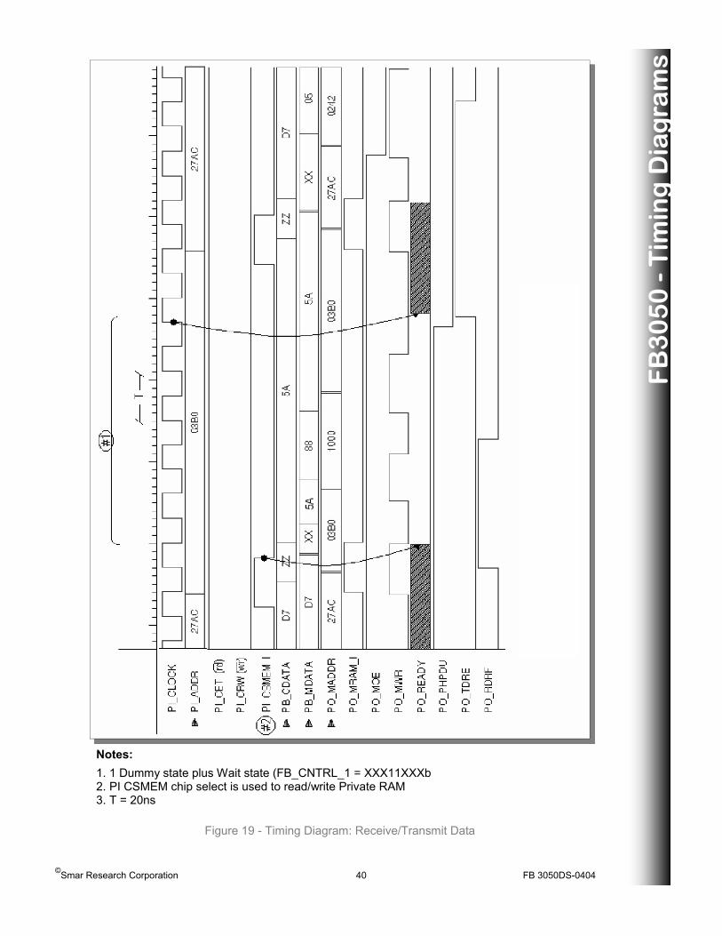
Figure 19 - Timing Diagram: Receive/Transmit Data
Notes:
1. 1 Dummy state plus Wait state (FB_CNTRL_1 = XXX11XXXb 2. PI CSMEM chip select is used to read/write Private RAM 3. T = 20ns
FB
30
50
- T
imin
g D
iag
ram
s

©Smar Research Corporation 41 FB 3050DS-0404
Figure 20 - FB3050 Mechanical Specifications
1.00
16.00 +/- 0.10
14.00 =/- 0.05
0.50
0.22 +/- 0.05
12.00 =/- 0.10
0.14 +/- 0.05
0 - 70
0.40 +/- 0.15
1.1 +/- 0.06
14.00 =/- 0.05
16.00 =/- 0.10
1.6 +/- 0.15
Dimensions in millimeters 100 PIN TQFP
FB
30
50
- M
ech
an
ica
l Sp
ec
ific
atio
ns

©Smar Research Corporation 42 FB 3050DS-0404
Symbol Parameter Min. Max. Units Notes
Vdd DC Supply Voltage -0.3 6.0 V
Vin Input -0.3 VDD + 0.3 V
Iin Input Pin Current -10.0 10.0 mA 25o
Ta Operating Free-Air Temperature -40 +85 C
Tstrg Storage Temperature -55 150 C
Tlead Lead Temperature 300 C 10 Sec
Table 11 - Absolute Maximum Ratings
Absolute Maximum Ratings
Symbol Parameter Min. Max. Units Notes Vdd-1 5V DC Supply Voltage 4.5 5.5 V
Vdd-2 3V DC Supply Voltage 2.7 3.3 V
Idd Static Supply Current 100 uA
Vil Input Low Voltage -0.3 0.3Vdd V
Vih Input High Voltage 0.7Vdd Vdd+0.3 V
Operating Conditions
Table 12 - Operating Conditions
Symbol Parameter Min. Max. Units Notes Iin Input Leakage Current (Inputs) (I/O) ±1.0 ±10.0
Ioh Output High Current Voh = 2.4V -4.0 mA
Iol Output Low Current Vol = 0.4V 4.0 mA
Ioz Tri-state Leakage Current PO_READY PO_PHPDU -10 10
DC Characteristics
Table 13 - DC Characteristics
FB
30
50
- D
evic
e C
ha
rac
teri
stic
s

©Smar Research Corporation 43 FB 3050DS-0404
Smar Research Corporation 4250 Veterans Memorial Highway
Holbrook, NY USA 11741 Tel: 631.737.3111 Fax: 631.737.3892
[email protected] www.SmarResearch.com
Smar Research reserves the right to make changes to design and functionality of any product without notice. Smar Research does not assume any liability arising out of the application or use of any product. Smar Research , Technology Source, and the SRC logo are registered trademarks of Smar Research Corporation. The HART, Fieldbus, and Profibus Foundation logos are
trademarks of their respective owners.