smart cmos focal plane arrays: a si cmos detector...
TRANSCRIPT

Smart CMOS Focal Plane Arrays:A Si CMOS Detector Array and Sigma Delta Analog to Digital Converter
Imaging System
Youngjoong Joo, Jinsung Park, Mikkel Thomas, Kee Shik ChungMartin A. Brooke, Nan M. Jokerst, D. Scott Wills
School of Electrical and Computer EngineeringGeorgia Institute of Technology
Atlanta, Georgia 30332Tel. 404-894-3304
Email: [email protected]
Abstract
This paper evaluates the potential for the rea time utilization of high frame rate imagesequences using a fully parallel readout system. Multiple readout architectures for high framerate imaging are compared. The application domain for a fully parallel readout system isidentified, and the design for a fully parallel, monolithically integrated smart CMOS focal planearray is presented. This focal plane image processing chip, with an 8 x 8 array of Si CMOSdetectors which each have a dedicated on-chip current input first order sigma delta analog todigital converter front end, has been fabricated, and test results for uniformity and linearity arepresented.
1. Introduction
Imaging detector arrays and image processing circuits are critical components in
many consumer, industrial, and military focal plane imaging array systems. System
specifications emphasize different aspects of imaging array technology, including high
frame rate, large array size, high fill factor, and high pixel resolution. Over the past
several years, significant advances in focal plane array (FPA) development have been
achieved. The number of pixels has increased to several thousand on a side, and the
resolution of the arrays also has been increased [1].The combination of higher resolution
with a larger number of pixels has resulted in data rates that can not be transmitted off of
the FPA through a one-port readout system. This data bottleneck is exacerbated when the
application demands high frame rates, which further challenge the data transfer rate off of
the FPA. Important emerging high speed imaging applications include combustion,
transMach fluid flow, and aerooptic sensing, which required high speed data rates that
cannot be handled by conventional image data transfer methods [2] [3] [4].

In addition to enhanced detector array performance, the integration of image
processing circuitry on the focal plane, or the realization of “smart” focal plane arrays, is
an area of research under intense study [Error! Bookmark not defined.]. Through
preprocessing of the raw image signal using on focal plane integrated circuitry, the data
transfer performance limitation of the imaging system can be addressed. Conventional
imaging systems use X-Y readout of the sensor array data followed by transportation of
the data to an off-chip serial analog-to-digital (A/D) converter (ADC). On-chip A/D
conversion is potentially a superior choice for an integrated imaging/preprocessing smart
imager, since it can reduce the cost, complexity, weight, and pick-up noise of the FPA
system. The noise bandwidth depends on the on-chip architecture. Three different on-
chip readout systems have been developed [1][5][6]. The first is a serial readout system,
involving X-Y multiplexing of sensor data to a single on-chip ADC. The second
approach is a semi-parallel readout system with an ADC for each column. The third
option is a parallel readout system with an ADC dedicated to each pixel.
The parallel readout system is the best choice to accommodate ever increasing
data rates for off-chip data transfer. This option performs the A/D conversion as early as
possible in a signal chain to avoid processing and transportation of analog signals, and
instead, utilizes the digital processing capability of modern CMOS processes. The per
pixel A/D conversion is the extreme of this solution, namely, associating one ADC with
each pixel. The advantages to this approach are that no signal degradation occurs when
digital data is read out of the detector array, and the incident signal on the detector can be
sensed and electrically integrated during the entire frame period. When this parallel
readout architecture is combined with a three dimensional (3D) through-Si vertical
optical communication link, a truly fully parallel readout system can be realized. Using
this architecture, a virtually unlimited scalable high speed readout system for a FPA
system can be demonstrated.
This paper explores the design and implementation of a smart FPA using an
integrated detector array and signal processing circuitry. Si CMOS detectors have been
used for the imaging detector array, which are integrated directly with per-pixel Si
CMOS sigma delta ADCs, which preprocess the detected image signals. Performance
data for this integrated smart FPA is included herein. In a future system, these FPA

signals can be passed down through a Si CMOS emitter driver which has been integrated
onto the imaging chip for 3D vertical through-Si data transfer to a second chip containing
an image processor. The design of the smart FPA is explored in the context of the final
two layer image processing system.
2. Architecture
To achieve image processing systems that operate in real time, on large images
with frame rates in the high kHz or MHz is beyond the capability of today’s imaging
systems. For example, a first-order sigma delta analog-to-digital converter (ADC)
generating a sequence of 500x500 8 bit images at a frame rate of 100 kHz must be
clocked at more than 655 GHz, which is far from practical. Even when parallel ADCs are
placed along the edge of the imaging array, the problem is only partially mitigated
because the speed at which the ADCs must operate still increases with image size. To
generate 500x500 8 bit images at a frame rate of 100 kHz, we need 500 ADCs, on the
same die, clocked at more than 1.31 GHz [7]. It is beyond any current technology to
make that many high speed ADCs on one die. Thus, serial ADCs are inadequate for this
task, and highly parallel ADCs must be examined for evolving high data rate systems.
In this paper, a fully parallel readout system is designed as a scalable FPA readout
system. This readout system provides a scaleable solution to the real time high frame rate
image capture problem when it is coupled to a massively parallel optically interconnected
processor. To keep the design scaleable, the processors must reside beneath the imaging
chip, which, in the final system, will use a through-Si vertical 3-D optoelectronic
interconnect for parallel connection to the detector plane. This is a scaleable design,
since, as the image size increases, the number of parallel vertical optical 3D links and the
number of processors in the array can increase accordingly, thus maintaining the frame
rate. The system design, using a through-Si integrated parallel optical data link is
illustrated in Figure 1(a).
The fully parallel readout system was designed so that each pixel has an
associated ADC, and subarrays of these pixels/ADCs are served by one vertical optical
link and one digital signal processing (DSP) unit to perform image processing. Each
pixel has an associated ADC. To maximize the imager fill factor, it is necessary to

minimize the area of the ADC circuitry. Thus, only the front end of the sigma delta ADC
was implemented on a per pixel basis in the detector array. To maximize the imager fill
factor, it is necessary to minimize the area of the ADC circuitry. Thus, a first order
current input sigma delta oversampling ADC was chosen because it is possible to
conserve space by only implementing the front end of the sigma delta A/D converter on a
per pixel basis on the detection plane. . The advantage of this architecture is that the
sigma delta ADC front end produces digital data, so further noise cannot be introduced to
the signal by shifting the digital data. This is in contrast to analog data, which is the data
format used in conventional FPA data links. An integrated optoelectronic emitter on each
sub-array allowed through-silicon wafer output of digital image data from the focal plane
to the processor stacked below each sub-arrays as shown in Figure 1. An integrated
optoelectronic emitter on each subarray allows vertical through-Si output of digital image
data from the focal plane to the processor stacked below each focal plane imager. These
integrated through-Si vertical optical data links have been demonstrated using stacked
foundry Si CMOS circuits, and are a viable technology for 3D system integration. This
3D vertical coupling to the image plane allows the detector and processor arrays to be
scaled while maintaining a fixed level of processing per pixel, as shown in Figure 1.
Thus, the processing rate is independent of the total imager array size, resulting in a
scalable readout system. The number of pixels in the subarray depends upon the
bandwidth of associated processor circuitryFor example, the type of processor used is this
design is the SimPil processor [8][9]. If an 8x8 sub-array is used, the size of the
processor and focal plane sub-array seems to match reasonably well: an 256×256 pixel
imaging array with 8 bits of resolution on the focal plane could be achieved by tiling an
8x8 array of processors each operating at 168 MHz.

Detectors and ADCs layer DSP layer
Through waferoptical
communication
Figure 1. A stacked two layer focal plane processor
An image sensor 8x8 subarray of detectors and per pixel sigma delta ADCs have
been designed, fabricated, and tested in digital Si CMOS. Figure 2 is an illustration of the
implemented image sensor subarray. Each subarray consists of an array of 8X8
multiplexed pixel blocks, each consisting of a photodetector and single sigma delta front
end ADC. Each pixel block was connected to a bit line using a pass transistor The bit
lines are read using a 8 row address decoder and an array of 8 digital sense amplifiers.
Each pixel block converts the analog light intensity into a digital signal. The entire
system is synchronous, and after each clock pulse, every pixel block produces one bit of
data. This generated a two dimensional array of bits. All the generated digital output
signals were amplified by the emitter driver to drive an integrated optoelectronic emitter
on each sub-array, optically interconnecting the imaging/preprocessing array to the
SIMPil processor on the second level of circuitry.

ReceiverComparatorSimPil
processor
Emitter
Emitter
Detector
After the optical signal is received by the receiver located on the second level of
circuitry underneath the focal plane array, the optic signal is amplified and synchronized
to the SimPIL digital signal processor by a clocked comparator. The serial output of the
comparator is read into the SimPil processor by serial to parallel conversion. The signal
path from image detector to signal processor is shown in Figure 2. To achieve a 100 kHz
frame rate, each SimPil processor needs to process data at 167 Mbps (for an 8x8 sub-
array image oversampled by 26). Assuming that a fully pipelined 8 bit processor is
clocked at 167 MHz, a frame rate of 100 kHz is possible.
Figure 2. Signal flow of the FPA sub-array
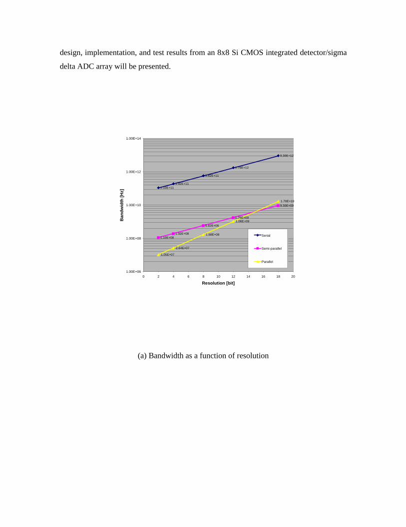
A readout speed comparison for different architectures is instructive. Figure 3
shows simulation results of the bandwidth as a function of resolution and array size for
three different architectures. Figure 3(a) was obtained under following assumptions: the
array size was 1000 x 1000; the frame rate of the system was 100 kfps; and 8 x 8
detection arrays were used for subarrays of a larger array size fully parallel system.
These assumptions dictate the bandwidth of the first order sigma delta ADC, which is
168 MHz for a parallel system, 2.62 GHz for a semiparallel system, and 2.62 THz for a
serial readout system. The system bandwidth was the same as the A/D converter
bandwidth for the parallel and serial systems, but it was increased for the semiparallel
readout system because there was only one processor for the whole FPA system.

Figure 3(b) is another simulation result, with fixed 8 bit resolution and different
array sizes. The bandwidth of parallel system was independent of the array size.
However the semiparallel and serial readout system bandwidths exponentially increased
with array size. From the simulation results, semi-parallel readout system have less
bandwidth, compared to the parallel readout system, when it was smaller than a 64 x 64
array size. These simulation results arose from the assumption that each row had its own
signal processor for the semiparallel system. If there was only one processor for the
whole system, the semiparallel system bandwidth would be the same as serial readout
system. From the above two graphs, it is clear that the parallel readout system had less
bandwidth than the other two readout systems, yet had the same resolution and array size.
(a) Bandwidth vs. resolution
1.64E+114.13E+11
2.62E+12
1.66E+13
1.06E+14
1.64E+084.13E+08
2.62E+09
1.66E+10
1.06E+11
1.05E+072.64E+07
1.68E+08
1.06E+09
6.76E+09
1.00E+00
1.00E+02
1.00E+04
1.00E+06
1.00E+08
1.00E+10
1.00E+12
1.00E+14
1.00E+16
0 2 4 6 8 10 12 14 16 18
Resolution [bit]
Ban
dwid
th [H
z]
Serial
Semi-parallel
Parallel

(b) Bandwidth vs. array size
Figure 3. Readout system bandwidths
To compare the bandwidths of the readout systems, it was assumed that
the same type A/D converter was used for different readout systems. This assumption
would not produce an optimal system if there were no area and power consumption
restrictions. For the semiparallel readout system, it is a more optimal solution to use
second-order sigma delta ADCs rather than first order sigma delta ADCs so long as the
larger area is available. By using second-order sigma delta ADCs, the oversampling ratio
can be decreased significantly [10]. Likewise, for serial readout systems, there is no
limitation in choosing an ADC type. In the following simulations, a second-order sigma
delta A/D converter was used for comparison. All the other assumptions were the same
as previously stated. Figure 4(a) is an interesting simulation result shwoing bandwidth as
a function of resolution. At resolutions over 15 bits, the semiparallel readout system
resulted in less bandwidth, compared to the parallel readout system (although the 4 GHz
bandwidth is a challenging ADC bandwidth to achieve). Figure 4(b) showed another
interesting simulation result: the semiparallel readout system is better for array sizes
under 288x288 provided that a signal processor supports each row.
Thus, for low resolution and large image arrays, the parallel readout system has
the best performance for low resolution and large image arrays. In the next sections, the
1.68E+08
1.68E+10
1.68E+12
1.68E+14
2.10E+07
2.10E+08
2.10E+09
2.10E+10
1.68E+08 1.68E+08 1.68E+08 1.68E+08
1.00E+07
1.00E+08
1.00E+09
1.00E+10
1.00E+11
1.00E+12
1.00E+13
1.00E+14
1.00E+15
1 10 100 1000 10000
Array size
Ban
dwid
th [H
z]
Serial
Semi-parallel
Parallel
design, implementation, and test results from an 8x8 Si CMOS integrated detector/sigma
delta ADC array will be presented.
(a) Bandwidth as a function of resolution
1.10E+111.92E+11
5.82E+11
1.76E+12
9.30E+12
1.10E+081.92E+08
5.82E+08
1.76E+09
9.30E+09
1.05E+07
2.64E+07
1.68E+08
1.06E+09
1.70E+10
1.00E+06
1.00E+08
1.00E+10
1.00E+12
1.00E+14
0 2 4 6 8 10 12 14 16 18 20
Resolution [bit]
Ban
dwid
th [H
z]
Serial
Semi-parallel
Parallel

(b) Bandwidth as a function of array size.
Figure 4. Readout system bandwidths with different ADC
3. Sigma Delta Analog to Digital Converters
Modern short-channel CMOS processes offer a speed performance which
is often far beyond system requirements. Speed will continue to improve as shorter
channel lengths are available in the future. Accuracy and the component matching,
however, are expected to become worse with decreasing linewidth. For a fully parallel
FPA system, this is a potentially serious problem because there are thousands of ADCs
working together, which necessitate good device uniformity to produce a uniform image.
Hence, it is an advantage to trade off speed and accuracy, thus resulting in a flexible
system, which enables access to higher accuracy at the cost of speed degradation. This
trade off can be realized using an oversampling converter, which is an ADC that trades
off speed and component mismatch. An example of one such ADC is a sigma delta
current input 1st order modulator. The simplified architecture of this ADC is shown in
Figure 5. The blocks that make up the system will now be briefly described.
3.72E+07
3.72E+09
3.72E+11
3.72E+13
4.65E+06
4.65E+07
4.65E+08
4.65E+09
1.68E+08 1.68E+08 1.68E+08 1.68E+08
1.00E+06
1.00E+07
1.00E+08
1.00E+09
1.00E+10
1.00E+11
1.00E+12
1.00E+13
1.00E+14
1 10 100 1000 10000Array size
Ban
dwid
th [H
z]
Serial
Semi-parallel
Parallel
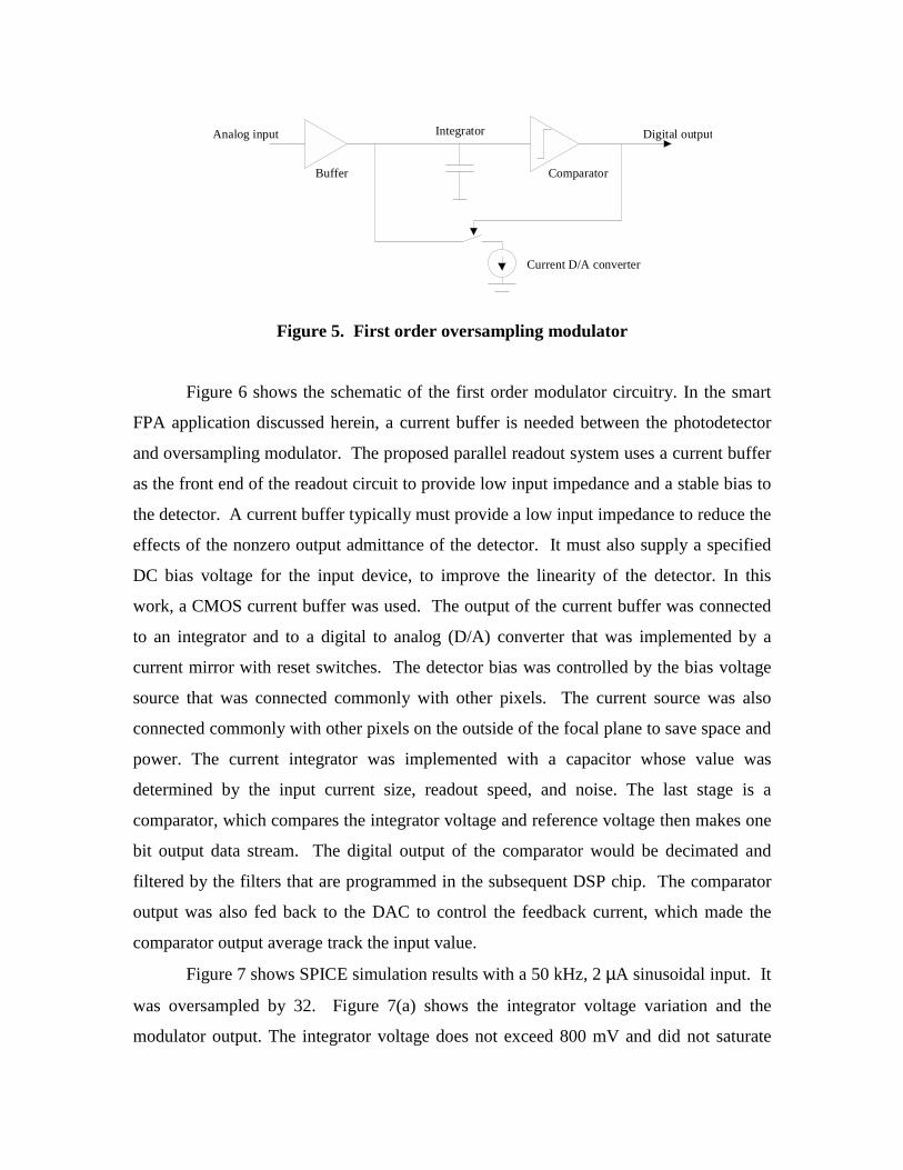
Figure 5. First order oversampling modulator
Figure 6 shows the schematic of the first order modulator circuitry. In the smart
FPA application discussed herein, a current buffer is needed between the photodetector
and oversampling modulator. The proposed parallel readout system uses a current buffer
as the front end of the readout circuit to provide low input impedance and a stable bias to
the detector. A current buffer typically must provide a low input impedance to reduce the
effects of the nonzero output admittance of the detector. It must also supply a specified
DC bias voltage for the input device, to improve the linearity of the detector. In this
work, a CMOS current buffer was used. The output of the current buffer was connected
to an integrator and to a digital to analog (D/A) converter that was implemented by a
current mirror with reset switches. The detector bias was controlled by the bias voltage
source that was connected commonly with other pixels. The current source was also
connected commonly with other pixels on the outside of the focal plane to save space and
power. The current integrator was implemented with a capacitor whose value was
determined by the input current size, readout speed, and noise. The last stage is a
comparator, which compares the integrator voltage and reference voltage then makes one
bit output data stream. The digital output of the comparator would be decimated and
filtered by the filters that are programmed in the subsequent DSP chip. The comparator
output was also fed back to the DAC to control the feedback current, which made the
comparator output average track the input value.
Figure 7 shows SPICE simulation results with a 50 kHz, 2 µA sinusoidal input. It
was oversampled by 32. Figure 7(a) shows the integrator voltage variation and the
modulator output. The integrator voltage does not exceed 800 mV and did not saturate
Analog input Digital output
Current D/A converter
Integrator
Buffer Comparator

Integrator output voltage
Modulator
with maximum input current. The 800 mV resulted from the assumption of an 8 bit, 100
kfps system with maximum 2 µA input current and an 800 fF integrator size. The power
density function (PDF) of the output code is shown in Figure 7(b). Consistent with
sigma-delta modulator properties, the noise increases with frequency. The modulator
output signal was decimated and low pass filtered to produce the binary output code.
Figure 6. First order oversampling modulator with current buffer
(a) Integrator and output nodes voltage

0 5 10 15
x 105
-60
-50
-40
-30
-20
-10
0
10
20
30
Frequency
PDF [dB]
50 kHz input signal
Modulation noise
125←m
125←m
40←m77←m
60←m
35←m
27←m
(b) Power density function
Figure 7. First order oversampling modulator simulation results
Figure 8 shows a layout and photomicrograph of the modulator circuits for FPA
pixel. All the circuits, including the data lines and detector, were laid out to fit into a 125
µm X 125 µm area. The design of compact circuits was essential so as to enable a large
detector and capacitor. All surfaces except the detector were covered by metal 3 to
prevent extraneous current charge through the circuit area.
a) A single integrated detector/ADC pixel: layout.

Detector Capacitor
Circuits
(b) A single integrated detector/ADC pixel: photomicrograph.
Figure 8. Layout and photomicrograph of a single integrated detector/ADC pixel.
4. CMOS Image Sensor
To integrate the detector imaging array onto the silicon circuitry, there are two
options which can be explored. One is a hybrid integrated detector array [11], and the
other is a monomaterial detector [12]. The advantages of the hybrid detector are a higher
fill factor since the detectors can be integrated directly on top of the circuitry, and
independent optimization of the detector and the circuitry. Thus, the performance of the
array can be significantly improved, but the system cost is higher since there is an
assembly cost associated with the hybrid integration. The other image sensor that can be
used accesses monomaterial integration for the detector, i.e., implementing the detector
directly in the Si CMOS. The responsivity and wavelength of operation are limited, as is
the fill factor, however, for many applications, the use of Si detectors is adequate.
CMOS-based image sensors offer the potential opportunity to integrate a significant
amount of VLSI electronics on chip, and reduce component and packaging cost. A
number of types of Si CMOS photodetectors have been reported in the literature. In this
paper, a photodiode was used for the photodetector instead of a phototransistor because
the photodiode has better linearity [13]. Additional problems are noise level and
scalability. The Si CMOS pixel does not scale well to a larger array size and a faster
pixel readout rate, since the bus capacitance and the readout noise increases. In this
n p
Vbi Gn np p p
p
V
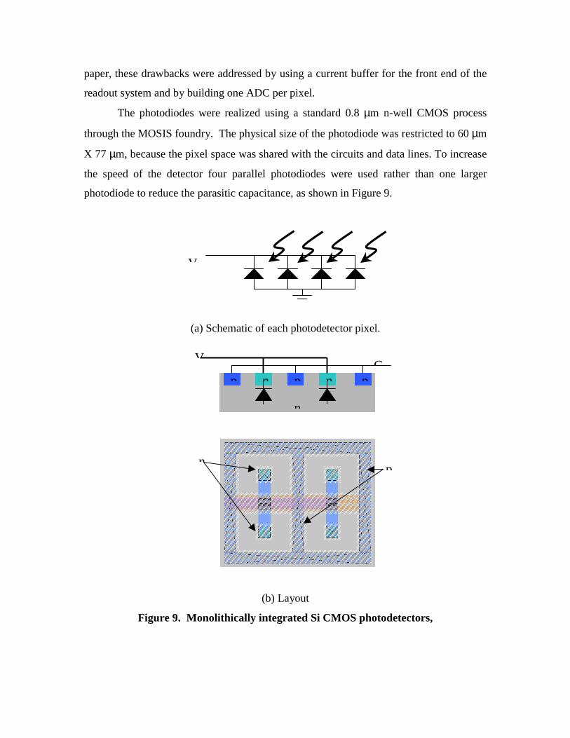
paper, these drawbacks were addressed by using a current buffer for the front end of the
readout system and by building one ADC per pixel.
The photodiodes were realized using a standard 0.8 µm n-well CMOS process
through the MOSIS foundry. The physical size of the photodiode was restricted to 60 µm
X 77 µm, because the pixel space was shared with the circuits and data lines. To increase
the speed of the detector four parallel photodiodes were used rather than one larger
photodiode to reduce the parasitic capacitance, as shown in Figure 9.
(a) Schematic of each photodetector pixel.
(b) Layout
Figure 9. Monolithically integrated Si CMOS photodetectors,

5. System Test Results
To verify that the system was working properly, a test image with a laser source
was used to project a simple image onto the FPAs. The He:Ne laser output was focussed
by a lens onto the 8 x 8 detector array FPA chip, and the position of the spot was varied
by changing the chip position. The system test was performed with two different
microprocessors. One was a 50 MHz 486 processor, and the other was a 233 MHz
Pentium processor. With the 486 processor, the data acquisiton rate was limited to 200
kHz. It was increased up to 1 MHz with the Pentium processor, a linear increase with the
clock rate of the data acquisition system, which suggests that the data acquisition rate was
limited not by the FPA readout system but by the test setup.
Figure 10(a) is an illustration with a photograph of the test setup. In the
photograph at right, the laser, lens, and a patterned image are shown. The chip could be
translated in the x, y, and z directions. The output was displayed on the monitor after
averaging the output data. The averaging is a function of the filter implemented on the
DSP, and can be varied to trade off resolution and speed. This adaptability is a particular
strength of sigma delta ADCs. Figure 10(b) shows a 4 bit image with 1 MHz clock rate,
averaging 16 samples. The data on the screen, as shown in Figure 10(a), were numerical
values with an approximately linear relationship between the detected optical intensity
and the numerical value. In Figure 10(b), data are presented for the laser spot in various
spatial locations on the FPA. The most highly illuminated pixel was colored white, and
the darkest pixel was colored black, with gray scale between the two extremes of
illumination.
(a) Test setup
1 1 2 11 8 6 4 11 2 5 8 11 11 5 11 4 16 10 16 16 16 25 4 10 16 16 16 16 13 5 16 16 16 16 16 13 3 8 16 16 16 10 01 2 2 10 16 11 11 11 0 2 2 6 4 4 1

(b) Computer screen images, resolution: 4bits, frame rate: 3.9 kfps
Figure 10. FPA functional test
Uniformity is one of the important characteristics of an imaging system. To get a
good quality image with a minimum of correction needed, all detectors and their
associated circuitry needs to respond to optical input uniformly. To measure the
uniformity of the system described herein, a test was run with the readout system running
below a 1 MHz system clock frequency, and the maximum data value was set to 64. An
uncalibrated halogen light source which was large in comparison to the FPA size was
used to illuminate the FPA from a distance of 3 m to produce a uniform intensity across
the FPA. Figure 11 shows the test results of FPA uniformity. Standard deviation among
the pixels was calculated to measure the uniformity. Twelve different light intensity
values were used to measure the uniformity, and most showed good standard devination
across the array. Table 1 shows the measured standard deviation for all 12 different
optical input intensities. The test results included all noise sources from the detector and
circuits. These test results show that the standard deviation decreased with increasing
input intensity. The optical intensity was controlled using neutral density filters to
generate outputs between 0 and 64. The last test result in Table 6.3 was not valid because
the circuit was saturated. The optical input intensity is reported as a percentage of the
maximum incident optical input. When the optical input was more than 15% of
maximum, the output was saturated.

12 3
45
67
8S1
S2
S3
S4
S5S6
S7S8
0
4
8
12
16
20
24
28
32
36
40
44
48
52
56
60
64
Output
X
Y
Maximum : 47.95Minimum : 45.48Average : 46.39Standard diviation :0.4741 (1.022%)
12
34
56
78
S1
S2
S3
S4
S5
S6S7
S8
0
4
8
12
16
20
24
28
32
36
40
44
48
52
56
60
64
Output
X
Y
Maximum : 6.90Minimum : 6.05Average : 6.31Standard diviation :0.1365 (2.165%)
(a) Low optical input intensity
(b) High optical input intensity
Figure 11. Uniformity test results

Table 1 Uniformity under different optical input intensities.
Light
Intensity
Maximum
(64)
Minimum
(64)
Average
(64)
Standard
Deviation
%
(100)
0.0316% 0.62 0.48 0.52 0.0217 4.19
0.0501% 0.66 0.52 0.56 0.0225 4.04
0.1% 0.96 0.74 0.79 0.0343 4.33
0.158% 1.38 1.12 1.18 0.0390 3.30
0.316% 2.22 1.85 1.95 0.0579 2.97
0.501% 3.55 3.02 3.18 0.0854 2.69
1% 6.90 6.05 6.31 0.1365 2.17
1.583% 9.90 8.74 9.11 0.1965 2.16
3.16% 16.97 15.02 15.68 0.3385 2.16
5.01% 25.95 23.46 24.44 0.4273 1.75
10% 47.95 45.48 46.39 0.4741 1.02
*15.83% 62.83 62.29 62.56 0.1073 0.17
* Saturated
Photodetector linearity was tested with the halogen optical source and four neutral
density filters. By combining the four optical filters, 16 different optical input intensities
were measured. However, the circuit was saturated with 5 out of 16 light intensities, and
they were removed from the evaluation. Figure 11(a) shows the linearity of all of the 64
pixels, and (b) shows 6 bits resolution for a single pixel. Over the majority of the range
of the input optical intensities, 6 bit linearity has been demonstrated.

(a) Data from all 64 pixels.
(b) A single pixel, with 6 bits of linearity.
Figure 11. Linearity test results
6. Conclusions
In this paper, a scalable fully parallel readout system for focal plane arrays is
demonstrated. To realize a high speed parallel readout system, a compact size 1st order
current input sigma-delta modulator was designed to support each pixel in the imaging
0
10
20
30
40
50
60
0 10 20 30 40 50 60 70 80 90 100
Light intensity
Out
put
0
10
20
30
40
50
60
0 10 20 30 40 50 60 70 80 90 100
Light intensity
Out
put

array. From the speed comparison simulations, the proposed readout system has an
advantage when it is used for large array sizes with a medium resolution range. An 8 x 8
detector array with an ADC front end dedicated to each pixel was implemented and tested
in Si CMOS. Test results on the FPA indicate good array uniformity and linearity.
References
[1] Zhimin Zhou, Bedabrata Pain, Roger Panicacci, Barmak Mansoorian, Junichi Nakamura,Eric R. Fossum, “On-Focal-Plane ADC: Recent Progress at JPL,” Proceedings of SPIE - TheInternational Society for Optical Engineering, vol. 2745, pp. 111-122, 1996.
[2] Paul F. Goldsmith, “Focal plane arrays for millimeter-wavelength astronomy,” IEEE MTT SInt Microwave Symp Dig, vol. 3, pp. 1255-1258, 1992.
[3] George J. Yates, Nicholas S. King, “High-frame-rate intensified fast optically shuttered TVcameras with selected imaging applications,” SPIE, vol. 2273, pp. 126-149, 1994.
[4] Richard B. Sanderson, “Infrared missile warning sensors,” IEEE Proc Natl Aerosp ElectronConf, vol. 2, pp. 777-781, 1996.
[5] Bedabrata Pain, Eric R. Fossum, “Approaches and Analysis for On-Focal-Plane Analog-to-Digital Conversion,” Proceedings of SPIE - The International Society for OpticalEngineering, vol. 2226, pp. 208-218, 1994.
[6] Ulf Ringh, Christer Jansson, Kevin Liddiard, “ Readout Concept Employing a Novel onChip 16bit ADC for Smart IR Focal Plane Arrays,” Proceedings of SPIE - The InternationalSociety for Optical Engineering, vol. 2745, pp.99-110, 1996.
[7] Youngjoong Joo, S. Fike, Kee Shik Chung, Martin A.Brooke, Nan M. Jokerst, Scott Wills, “Application of Massively paralll Processors to real time processing of high speed images,”MPPOI, pp.96-100, 1997.
[8] H. H. Cat., J. C. Eble, D. S. Wills, V. K. De, M. Brooke, N. M. Jokerst, Low PowerOpportunities for a SIMD VLSI Architecture Incorporating Integrated OptoelectronicDevices, GOMAC’96 Digest of Papers, pages 59-62, Orlando, FL, March 1996.
[9] Huy H. Cat, D. Scott Wills, Nan Marie Jokerst, Martin A. Brooke, April S. Brown, “Three-dimensional, massively parallel, optically interconnected silicon computational hardwareand architectures for high-speed IR scene generation,” Proceedings of SPIE - TheInternational Society for Optical Engineering, vol. 2469, pp. 141-145, 1995.
[10] J. C. Candy, G. C. Temes, “A tutorial discussion of the oversampling method for A/D andD/A conversion,” Proceedings - IEEE International Symposium on Circuits and Systems,vol. 2, pp. 910-913, 1990.
[11] Fike, S.M., Buchanan, B., Jokerst, N.M., Brooke, M.A., Morris, T.G., DeWeerth, S.P., “8x8Array of Thin-Film Photodetectors Vertically Electrically Interconnected to SiliconCircuitry,” IEEE Photonics Technology Letters, vol. 7, no. 10, pp 1168-1170, October 1995.
[12] Antoine Dupret, Eric Belhaire, “A high current large bandwidth photosensor on standardCMOS processes,” Proceedings of SPIE - The International Society for OpticalEngineering, vol. 2950, pp. 36-44, 1996.
[13] Pallab, Bhattacharya, Semiconductor optoelectronic devices, Prentice Hall, 1994.