smart materials and surfaces sms bangkok 2014 international conference proceeding · pdf...
TRANSCRIPT

Smart Materials and Surfaces
SMS Bangkok 2014 International
Conference Proceeding
www.setcor.org/conferences/SMS-Bangkok-2014

Table of contents Smart Materials and Surfaces: Fabrication, Characterization & Properties
1.
Silicon Nitride Protective Coating by Gas-timing RF Magnetron Sputtering Deposition
N.Paleeya, N. Khemasiri, D. S-T Phromyothin, M. Horprathum, S.Porntheeraphat, J.Nukeaw and S. Pratontep; National Electronics and Computer Technology Center, Thailand Science Park and College of Nanotechnology, King Mongkut's Institute of Technology, Thailand
2.
Simple Methods to Fabricate Multilayer Microfluidic Devices
T. Jiemsakul, C. Kortchana, S. Manakasettharn National Nanotechnology Center, Integrated Nanosystem Laboratory, Pathum Thani and King Mongkut’s Institute of Technology Ladkrabang, College of Nanotechnology, Bangkok, Thailand
Smart Materials and Surfaces for Energy and Environment
1
Electrochromic Materials and their Characterization by Solar Radiation Glazing Factors for Smart Window Applications
B. Petter Jelle, T. Gao and A. Gustavsen SINTEF Building and Infrastructure, Department of Materials and Structures, Norwegian University of Science and Technology (NTNU), Department of Civil and Transport Engineering and Norwegian University of Science and Technology (NTNU), Department of Architectural Design, History and Technology, Norway.
2
Molecular Simulations of Anti-stain Polymeric Coatings
Y. Singhvi, I. V. N. Tejasvini and G. Manik Department of Polymer and Process Engineering, IIT Roorkee (Saharanpur Campus), Saharanpur, India
3
Study of Electrical Conductivity of Polypyridine-PVAc Composite Thin-Film doped with Ni(NO3)2
G. R. Dhokane Department of Physics, Arts, Science & Commerce College, Chikhaldara, Maharashtra- India
4.
A Smart Material for Imaging Highway Substructure Damage
K. Rudahl and S. E. Goldin Department of Computer Engineering, King Mongkut's University of Technology, Thonburi, Thailand.
5
Application of Spark Plasma Sintering for Fabrication of Functionally Graded Thermal Barrier Coating on a Superalloy Substrate
M. Bahrami, A.H. Pakseresht and A. Simchi Department of Material Science and Engineering, Sharif University of Technology, and Department of Ceramics, Materials and Energy Research Center, Karaj, Iran
6
Synthesis and Optical Characterization of Ca2PO4Cl:Tb3+ and Mn2+ Green Emitting phosphor for solid state lighting
N.S. Kokode, V.R. Panse and S. J. Dhoble N.H.College,Bramhapuri,Gondwana University and Department of Physics, RTM Nagpur University, India
7
Development of Through Silicon Stacking Technology for Capacitive Acoustical MEMS Resonators
N. Belkadi, B. Dulmet and T. Baron FEMTO-ST Institute, Time and Frequency Dpt., Besançon, France
8
Establishment of Optimized Metallic Contacts on Porous Silicon for Thermoelectric Applications
O. Abbes, A. Melhem, K. Snabi, C. Leborgne and N. Semmar GREMI CNRS-Université d’Orléans, Orléans, France
9 Formation of magnetic phases by reactive diffusion between Mn and Ge for Spintronic Applications

O. Abbes, A. Portavoce, C. Girardeaux, A. Spiesser, and V. Le Thanh GREMI CNRS-Université d’Orléans, Aix-Marseille Université, CNRS, IM2NP-UMR 6242 and Aix-Marseille Université, CNRS, CINaM-UMR 7325, Marseille, France
10
Strength and Ductility of SGFRP Confined Concrete
Q. Hussain, A. Pimanmas and L. Lalin, Sirindhorn International Institute of Technology, Thammasat University, Thailand.
11
Smart Focused-Ion-Beam-fabricated Nanostructures for Improving Sur-face Enhanced Raman Scattering on Trace Detection of Single Molecules
K. Sivashanmugan, J-D Liao and C-K Yao Department of Materials Science and Engineering, Center for Micro/Nano Science and Technology, Nation-al Cheng Kung University, Taiwan.
12
Nanostructured metal oxides: catalyst-free synthesis, characterization and Integration with MEMS processing for gas sensor
S. Chandra and B. Behera Centre for applied Research in Electronics, Indian Institute of Technology Delhi, India
13
A Microscale Piezoelectric Harvester for Mechanical Energy from Fluid Flow
K. Koyvanich, N. Muensit and P. Smithmaitrie Center of Excellence in Nanotechnology for Energy (CENE), Physics Department, Faculty of Science and Department of Mechanical Engineering, Faculty of Engineering, Prince of Songkla University (PSU), HatYai, Songkla, Thailand.
14
Effect of electron beam on thermal, morphological and anti-oxidant properties of kraft lignin
T.Venkatappa Rao, N.Rajeswara Rao, SVS Ramana Reddy and B.Sanjeeva Rao National Institute of Technology, Warangal, India
15
Facile growth of carbon nanotube electrode from electroplated Ni catalyst for supercapacitors
V. Yordsri, W. Wongwiriyapan and C. Thanachayanont College of Nanotechnology, King Mongkut’s Institute of Technology Ladkrabang/ Nanotec-KMITL Center of Excellence on Nanoelectronic Device/ Thailand Center of Excellence in Physics/ National Metal and Materials Technology Center, Thailand
Smart Materials and Surfaces for life science
1.
Immobilization of Urease Based on Adsorption in Eggshell Membrane for Urea Biosensor Application
T. Suwanchaituch, S. Imthong and K. Panpae Department of Chemistry, Faculty of Science, King Mongkut’s University of Technology Thonburi, KMUTT, Bangkok, Thailand
2.
Needle-less Jet Injection System with Multi-Pore Nozzle for Viscous Drug Delivery Applications
Y. C. Jo, H. K. Hong, Y. S. Choi and H. S. Kim Korea Electronics Technology Institute, Medical IT Convergence Research Center, SeongNam-Si and Korea Electronics Technology Institute, Contents Research Center, SeongNam-Si, South Korea

xxx
Silicon Nitride Protective Coating by Gas-timing RF Magnetron
Sputtering Deposition
N. Khemasiri1, N. Paleeya
1, D. Sae-tang Phromyothin
1, M. Horprathum
2, S.Porntheeraphat
2, A. Sungthong
3
J. Nukeaw1 and S. Pratontep
1*
1College of Nanotechnology, King Mongkut’s Institute of Technology Ladkrabang, Bangkok 10520, Thailand 2National Electronics and Computer Technology Center (NECTEC), NSTDA, Pathumthani 12120, Thailand
3Rajanagarindra Rajabhat University, Chachoengsao 24000, Thailand
*Corresponding author. Tel: (+66) 3298000 ext. 3077; E-mail: [email protected]
Abstract: Protective coating based on silicon nitride
is a promising alternative to carbon based coatings,
owing to its compatibility with existing
semiconductor technology. However, the fabrication
of silicon nitride thin films, e.g. reactive sputtering
and chemical vapor deposition, often face difficulties
in obtaining desirable properties, owing to the
complexity of the process and contaminations. Here
we explore a method to better control the properties of
silicon nitride thin films from plasma sputtering
deposition by the gas-timing technique. The gas-
timing sputtering technique controls the on-off
sequence of the reactive sputtering gases during
deposition. In this study, Ar plasma sputtering with a
pure silicon target was employed. The Ar gas was
injected in alternation with N2 gas with the timing
ratio (in seconds) of Ar:N2 from 10:0, 10:1, 10:3,
10:5, 10:7 and 10:10. The effect of the gas-timing
ratio on the properties of silicon nitride films was
investigated by Atomic Force Microscopy, Raman
Spectroscopy, Auger Electron Spectroscopy, X-ray
Diffraction. The chemical resistance was measured by
electrochemical corrosion test in sulfuric acid, while
the hardness was obtained by the nano-indentation
technique. The results reveal that while the gas
timing technique is able to slightly vary the nitrogen
content in the films, other properties of the films are
significantly improved, such as surface morphology,
acid corrosion resistance, hardness properties.
Keywords: hard coatings, silicon nitride, corrosion,
plasma sputtering
Introduction
Silicon Nitride (Si3N4) is a promising candidate for
hard coating applications, owing to high corrosion
resistance, high hardness value, chemical and thermal
stability [1]. The main advantage is its compatibility
to the silicon-based microfabrication technology. In
general, silicon nitride coating may be fabricated by
several processes, such as chemical vapor deposition
[2]. However, such processes often require high
operating temperature and hazardous chemicals as the
nitrogen source. RF magnetron sputtering is an
alternative technique for silicon nitride fabrication,
which offers a low temperature operation, and high
film adhesion [3]. Conventional magnetron sputtering
with a homogenous mixture of sputtering gas and
reactive gas often has a drawback of the difficulties in
precisely controlling the properties. Recently, a novel
rf magnetron sputtering technique called “reactive
gas-timing” with an on-off sequence of reactive and
sputtering gases have been demonstrated in metal
oxynitride thin film fabrication with a precise control
the properties and the composition of the films [4,5].
In this research, silicon nitride thin films have
been fabricated by reactive gas-timing rf magnetron
sputtering system without substrate heating or
substrate bias. We investigate the effect of the
nitrogen timing (1, 3, 7 and 10 s) alternated with a
fixed Ar timing of 10 s on the properties of the
deposited films by atomic force microscopy, Raman
spectroscopy, Auger electron spectroscopy,
electrochemical corrosion test, and nanoindentation.
Experimental
Sputtered silicon nitride (SiNx) thin films with
different Ar:N2 timing ratios were fabricated onto p-
type si(100) and glass substrates by rf magnetron
sputtering system with reactive gas-timing technique
using a 99.999% silicon target. The target was also
cleaned by pre-sputtering with pure Ar at the start of
each run. The substrates were ultrasonically cleaned
in isopropanol alcohol, acetone, DI water and then
dried by N2.blow gun. The sputtering conditions are
listed in Table 1.
The properties of the deposited silicon nitride thin
films were investigated: surface morphology by
Atomic Force Microscope (AFM, Seiko SPI400) in
the non-contact mode, chemical composition by
Auger Electron Spectroscopy (AES, ULVAC PHI700,
Table 1: Sputtering parameters for SiNx deposition
Deposition parameter Condition
Base pressure 6.0 x 10⁻⁶
mbar
RF Power 80 W
Sputtering temperature Room temperature
Ar flow rate
N2 flow rate
10 sccm
3 sccm
Ar timing
N2 timing
10 sec
1, 3, 7, 10 sec
Film thickness 100 nm
Smart Materials and Surfaces : Fabrication, Characterization & Properties

xxx
measured at 10 nm below the surface), and chemical
bonding by Raman spectroscopy (Thermo Scientific
DXR Smart Raman). The anticorrosion performance
was studied by the electrochemical corrosion test
(Autolab PGST AT302) in 1M H2SO4 (Sigma-
Aldrich). The hardness of the silicon nitride coatings
was characterized by nanoindentation (Micro
Materials), with the load range of 0-1000 N using
the Berkovich tip.
Results and Discussion
Figure 1 shows the N:Si atomic composition ratio
obtained by AES as a function of the N gas-timing
duration. The content of N in the sputtered films
increases slightly with the N:Si ratios around 70-75%,
as the N injection duration expands. The AES results
also indicate that some oxygen is present in the films,
possibly for the background gases. The Raman results
(not shown) confirm a mixture of a Si-Nx phase and
possibly a Si or a Si-O phase.
From such small increase in the N content in the
films, other properties of the films are not expected to
vary greatly. Figure 2 illustrates that the root-mean-
square (rms) surface roughness measured by AFM
exhibit a sharp increase for the Ar:N2 timing ratio of
10:7. The corrosion test results as shown in Fig. 3 also
demonstrate such trend. The corrosive current
significantly decreases at high N timing, with the
lowest current at the 10:7 ratio.
Figure 4 illustrates the hardness and elastic
modulus results from the force-displacement curve
obtained by the nanoindentation. As the N timing
increases, the hardness of the silicon nitride films
gradually increases, while the elastic modulus exhibit
the opposite trend. In other words, at long N timing,
the films become stronger but less rigid. This suggests
that the timing sequence may induce better N-
incorporation and some structural differences in the
films, possibly multilayers.
Conclusions
This work demonstrate that N content may not be
the only factor that affects the film properties in
reactive sputtering processes. The reactive gas-timing
sputtering technique offers a better control of the
properties, together with the composition and the
structure of the films.
Acknowledgments
This work was supported by NECTEC-DSTAR,
Grant no. HDD-01-53-03M. We thank TMEC and
Suranaree University of the research facilities.
References
1. Krstic, Z., Krstic, V.D. (2012) J. Mater. Sci., 47,
535-552.
2. Oliphant, C.J., et al. (2013) Appl. Surf. Sci.,
285P, 440-449.
3. Zambom, L.S. et al. (2012) Microelectr. J., 40,
66-69.
4. Nukeaw, J., Sungthong, A., T-Thienprasert. et
al. (2008) App. Phys. Lett,. 93, 051903.
5. Klaitabtim, D., Pratontep, S., Nukeaw, J. (2008)
Ceram. Int., 34, 1103-1107.
Figure 2: Surface roughness (rms, 1 m
2 area) of
the silicon nitride thin films deposited with
different N timing.
Figure 3: I-V polarization curve of the silicon
nitride thin films in 1M H2SO4.
Figure 1: N:Si composition ratio of the silicon
nitride thin films as a function of N timing.
Figure 4: Hardness and elastic modulus of the
silicon nitride thin films deposited with different
N timing.
Smart Materials and Surfaces : Fabrication, Characterization & Properties

Simple Methods to Fabricate Multilayer Microfluidic Devices
T. Jiemsakul 1, C. Kortchana
2, S. Manakasettharn
1,*
1National Nanotechnology Center, Integrated Nanosystem Laboratory, Pathum Thani, Thailand
2King Mongkut’s Institute of Technology Ladkrabang, College of Nanotechnology, Bangkok, Thailand
*Corresponding author, [email protected]
ABSTRACT
Microfluidic devices have attracted wide attention with practical
applications to microtechnology and nanotechnology, primarily
due to their advantages such as low fluid volume consumption
and compactness of the devices. Microfluidic devices can consist
of one or more microchannels with at least one dimension less
than 1 mm. In traditional two-layer microfluidic devices, the
microchannels are fabricated on a substrate (the first layer) and
are then sealed with a cover plate (the second layer). In multilayer
microfluidic devices, longer microchannels can be fabricated to
achieve more performances. This work presents two simple
methods to fabricate multilayer microfluidic devices. For the first
method, we have used a CO2 laser beam to cut through 100-µm-
thick polyvinyl chloride (PVC) substrates to create
microchannels. For the second one, we have used the CO2 laser
beam to engrave microchannels on 1-mm-thick poly(methyl
methacrylate) (PMMA) substrates. The cover plates are made of
the same material. For both methods, we have used thermal
bonding to bond substrates and cover plates together. The PVC
microchannels resulting from the first method have approximately
rectangular cross-sections, where as the engraved PMMA
microchannels have approximately triangular cross-sections. The
depth of the PVC microchannels is controlled by the thickness of
the PVC substrates, whereas the depth of the engraved PMMA
microchannels depends on laser power. The width of
microchannels for both methods can be adjusted by varying the
laser power. Compared to conventional photolithography, these
two fabrication methods are simpler, faster, and cheaper. We
hope that these two methods will be implemented to manufacture
sophisticated multilayer microfluidic devices
Keywords
Microfluidic devices, microchannels, multilayer, fabrication, CO2
laser, polyvinyl chloride, PVC, poly(methyl methacrylate),
PMMA.
1. INTRODUCTION Microfluidic devices have received wide interest with practical
applications to microtechnology and nanotechnology, mainly due
to their advantages such as low fluid volume consumption and
compactness of the devices. As early as 1975, a microfluidic
device was fabricated on silicon using integrated circuit
technology consisting of a series of deposition, photolithography,
and etching steps [1]. Later, methods to fabricate microfluidic
devices have been developed [2]. This work presents simple
methods to fabricate microchannels using CO2 laser cutting and
engraving on substrates. Later, the substrates were thermally
bonded together to form closed microchannels and multilayer
microfluidic devices.
2. EXPERIMENTAL SECTION
2.1 Materials and apparatus We used 100-µm-thick polyvinyl chloride (PVC) transparency
sheets (OfficeMate Plc., Thailand) and 1-mm-thick poly(methyl
methacrylate) (PMMA) sheets (Panglas, Pan Asia Industrial Co.,
Ltd., Thailand) as substrates since they are transparent, thin,
cheap, and locally available. We used DraftSight and
LaserWorkV6 software to design microchannels. Later,
microchannels were fabricated on the substrates by the computer
controlled CO2 laser machine (SMLA-9060, Nextconcept9999
Co., Ltd., Thailand). Isopropyl alcohol (Fisher Scientific Ltd.,
UK) was used to clean the substrates. The fold back clips
(No.415/No.111, Horse, Nanmee Co., Ltd., Thailand) and the
microscope slides (No.7101, Sail Brand, China) were used to
clamp the substrates in the glass oven (B-585, Buchi (Thailand)
Co. Ltd., Thailand) for thermal bonding. The optical microscope
(BX51M, Olympus Corp., Japan) was used to characterize the
sizes of the fabricated microchannels.
2.2 Fabrication of PVC microchannels For the first method to fabricate microchannels, we used the CO2
laser beam to cut through the 100-µm-thick PVC substrates. To
form the closed microchannels, two PVC substrates were
thermally bonded on top and bottom of the PVC substrate with
the cut-through microchannels at 140 ̊C for 20 min. To form
multilayer microfluidic devices, multilayers of PVC substrates
with the microchannels were thermally bonded together.
2.3 Fabrication of PMMA microchannels For the second method, we used the CO2 laser beam to engrave
microchannels on the 1-mm-thick PMMA substrates. Another
PMMA substrate was thermally bonded on top of the PMMA
substrate with the engraved microchannels at 120 ̊C for 20 min to
form the closed microchannels. Multilayers of PMMA substrates
with the microchannels were thermally bonded together to form
multilayer microfluidic devices.
3. RESULTS AND DISCUSSION
Figure. 1 The optical microscope images showing the cross-
section of (a) a PVC microchannel and (b) a PMMA
microchannel.
Smart Materials and Surfaces : Fabrication, Characterization & Properties

Figure. 2 Relationships between laser power and geometrical
parameters of microchannels.
3.1 Laser cutting of PVC microchannels The CO2 laser machine generated the continuously focused laser
beam with a wavelength of 10.6 µm to heat the substrates. The
100-µm-thick PVC substrates were melted and cut through with
laser power of 11.6 W and above at the speed of the laser beam of
4 mm/s. The cross-section of the closed PVC microchannel is
approximately rectangular as shown in Figure.1(a). The influence
of laser cutting power on the width of the PVC microchannels is
shown in Figure.2. The average width of the cut-through PVC
microchannels increases linearly from 263 µm to 371 µm with the
laser cutting power varied from 11.6 W to 12.8 W at the constant
speed of the laser beam of 4 mm/s. The depth of the PVC
microchannels is controlled by the thickness of the PVC
substrates.
3.2 Laser engraving of PMMA microchannels Figure.1(b) shows the cross-section of a PVC microchannel
having approximately a triangular shape. Figure.2 presents the
influence of laser engraving power on the width and the depth of
the engraved PMMA microchannel. The laser engraving power
was varied from 11.4 W to 12.8 W at the constant speed of the
laser beam of 10 mm/s. The average depth of the PMMA
microchannels increases linearly with the laser cutting power from
95 µm to 456 µm while the average width of the PMMA
microchannels increases slightly 119 µm to 299 µm. Our results
of laser engraving on PMMA substrates and thermal bonding are
comparable to the previous work [3]. The 1-mm-thick PMMA
substrates are thick enough to use laser engraving in the range of a
set of the laser power mentioned above.
3.3 Multilayer microfluidic devices In this work, we fabricated two designs of multilayer microfluidic
devices with different materials, i.e. PVC and PMMA, using laser
cutting and laser engraving. Figure.3 presents schematic
illustrations of the exploded views of the fabricated multilayer
microfluidic devices in Figure.4. Figures.4(a),(c) show seven-
layer PVC microfluidic devices with total thickness of 0.7 mm.
Figures.4(b),(d) show 4.1-mm-thick multilayer microfluidic
devices consisting of four PMMA layers and a PVC bottom layer.
Figures.4(a),(b) show the multilayer microfluidic devices
consisting of three microchannels with red, green, and blue dyed
water inside crossing over and under each other. Figures.4(c),(d)
show the multilayer microfluidic devices consisting of the
microchannel with blue dyed water inside alternately crossing
over and under the microchannel with red dyed water inside.
With the same design of microchannels, using laser cutting of
microchannels requires more layers to form multilayer
microfluidic devices compared to using laser engraving of
microchannels.
Figure. 3 Schematic illustrations of the exploded views of
multilayer microfluidic devices in Figure. 4(a)-(d), respectively.
Figure. 4 A photograph of four fabricated multilayer microfluidic
devices next to the ruler.
4. CONCLUSION We have demonstrated the fabrication of the microchannels using
CO2 laser cutting on the 100-µm-thick PVC substrates and CO2
laser engraving on the 1-mm-thick PMMA substrates. The PVC
and the PMMA substrates were bonded thermally to form the
closed microchannels and multilayer microfluidic devices. The
cross-sections of the cut-through PVC microchannels and the
engraved PMMA microchannels are approximately rectangular
and triangular, respectively. The laser power has influence on the
width of the cut-through microchannels and the engraved
microchannels. The laser power also has influence on the depth
of the engraved microchannels, whereas the depth of the cut-
through microchannels is controlled by the thickness of the
substrates. These simple methods can be implemented in the
fabrication of sophisticated multilayer microfluidic devices.
5. ACKNOWLEDGMENT This work has been supported by the National Nanotechnology
Center (NANOTEC), Thailand.
6. REFERENCES [1] Terry, S. C. 1975. A Gas Chromatography System
Fabricated on a Silicon Wafer using Integrated Circuit
Technology. Ph.D. Dissertation, Stanford University,
Stanford, CA. Also, Stanford Electronics Laboratories
Technical Report No. 4603-1.
[2] Abgrall, P., and Gue, A.-M. 2007. Lab-on-chip technologies:
making a microfluidic network and coupling it into a
complete microsystem—a review. J. Micromech. Microeng.
17, 5 (Apr. 2007), R15-R19.
[3] Sun, Y., Kwok, Y. C., and Nguyen, N.-T. 2006. Low-
pressure, high-temperature thermal bonding of polymeric
microfluidic devices and their applications for
electrophoretic separation. J. Micromech. Microeng. 16, 8
(July 2006), 1681-1688.
Smart Materials and Surfaces : Fabrication, Characterization & Properties

1
Electrochromic Materials and their Characterization by Solar Radiation Glazing Factors for Smart Window Applications
Bjørn Petter Jelle ab*, Tao Gao c, Yingpeng Zhen b and Arild Gustavsen c
a SINTEF Building and Infrastructure,
Department of Materials and Structures, NO-7465 Trondheim, Norway.
b Norwegian University of Science and Technology (NTNU), Department of Civil and Transport Engineering, NO-7491 Trondheim, Norway.
c Norwegian University of Science and Technology (NTNU),
Department of Architectural Design, History and Technology, NO-7491 Trondheim, Norway.
* Corresponding author: [email protected] (e-mail), +47-73593377 (phone). Abstract Electrochromic materials (ECM) and windows (ECW) are able to regulate the solar radiation throughput by application of an external electrical voltage. Hence, as smart window applications, the ECWs may decrease heating, cooling and electricity loads in buildings by admitting the optimum level of solar energy and daylight into the buildings at any given time, e.g. cold winter climate versus warm summer climate demands. In order to achieve as dynamic and flexible solar radiation control as possible, the ECWs may be characterized by solar radiation glazing factors, i.e. ultraviolet solar transmittance (Tuv), visible solar transmittance (Tvis), solar transmittance (Tsol), solar material protection factor (SMPF), solar skin protection factor (SSPF), external visible solar reflectance (Rvis,ext), internal visible solar reflectance (Rvis,int), solar reflectance (Rsol), solar absorbance (Asol), emissivity (), solar factor (SF) and colour rendering factor (CRF). Comparison of these important solar quantities for various ECM and ECW combinations and configurations enables one to select the most appropriate ones for specific smart window and building applications.
Keywords: Electrochromic, Smart, Material, Window, Solar radiation, Solar factor, Solar heat gain coefficient. Introduction The application of electrochromic materials (ECM) in electrochromic windows (ECW) aims at controlling the solar radiation throughput at the earth’s surface, which is roughly located between 300 nm and 3000 nm. Such windows are often denoted smart windows. The ECW solar control is achieved by application of an external voltage. The visible (VIS) light lies between 380 and 780 nm. Ultraviolet (UV) and near infrared (NIR) radiation are located below and above the VIS region, respectively. Above 3000 nm, and not part of the direct solar radiation, lies the thermal radiation called infrared (IR) radiation, which all materials radiate above 0 K, peaking around 10 000 nm (10 m) at room temperature. However, the ECWs are not aimed at controlling the IR radiation. Normally, as low as possible heat loss through windows is desired, i.e. low U-value, which is accomplished by the application of various static low emissivity coatings on the window glass panes. Miscellaneous ECMs and ECWs and their various properties are investigated in the literature [1-10]. Some commercial ECWs are also already on the market [8,9]. ECMs and ECWs may also be used together with other materials and technologies, e.g. self-cleaning glazing materials and building integrated photovoltaics (BIPV) like solar cell glazing [11-15]. In general, it is of major importance to investigate the durability of building materials and components, also newly developed ones like e.g. ECMs and ECWs, which may be performed by carrying out accelerated climate ageing in the laboratory [16]. Thus, conducting a robustness assessment of these materials and components may also be found to be beneficial [17]. Hence, a durability and robustness evaluation of the new ECMs and ECWs should be carried out. This work presents two ECWs and their readily characterization by solar radiation glazing factors, i.e. ultraviolet solar transmittance (Tuv), visible solar transmittance (Tvis), solar transmittance (Tsol), solar material protection factor (SMPF), solar skin protection factor (SSPF), external visible solar reflectance (Rvis,ext), internal visible solar reflectance (Rvis,int), solar reflectance (Rsol), solar absorbance (Asol), emissivity (), solar factor (SF) and colour rendering factor (CRF). The solar factor (SF), which is the total solar energy transmittance, is also often denoted as the solar heat gain coefficient (SHGC) and the g-value. Further details about the solar radiation glazing factors are given in the literature [10,18,19]. Experimental For various experimental details concerning the synthesis and manufacturing of the ECMs and ECWs, and their electrochemical and spectroscopical characterization, it is referred to the studies by Jelle [10], Jelle and Hagen [20-22] and Jelle et al. [23]. In short, the ECMs polyaniline (PANI), prussian blue (PB)
Smart Materials and Surfaces for Energy and Environment Proceedings

2
and tungsten oxide (WO3) were deposited electrochemically onto transparent conducting glass plates coated with indium-tin-oxide (ITO), i.e. indium oxide doped with tin (In2O3(Sn)), whereas solid state ECWs were then constructed by applying the solid state polymer electrolyte poly(2-acrylamido-2-methyl-propane-sulphonic acid) (PAMPS) as an ionic conductor, see Fig.1 for a schematic drawing of the two ECWs presented here (denoted as ECW1 and ECW3).
Light
Glass Glass
Applied voltage
Indium-tin oxide
Tungsten oxidePolyaniline
Indium-tin oxide
Prussian blue
PA
MP
S
Figure 1. Schematic drawing of the ECW configuration used for ECW1 and ECW3 based on the ECMs polyaniline (PANI), prussian blue (PB) and tungsten oxide (WO3). Furthermore, for the spectroscopical measurements, a Cary 5 UV-VIS-NIR spectrophotometer, with an absolute reflectance accessory (Strong-type, VW principle), was used to measure the transmittance and reflectance of the ECWs, whereas emissivity measurements were performed with a SOC-100 HDR Hemispherical Directional Reflectometer from Surface Optics Corporation connected to a Thermo Nicolet 8700 Fourier transform infrared (FTIR) Spectrometer. Results and Discussion Measured transmittance spectra for two different ECWs at various applied electrical potentials (voltages) are given in Fig.2, with corresponding calculated solar radiation glazing factors and factor modulations in Table 1 and Table 2, respectively.
As to show an example how to calculate the solar radiation glazing factors, the solar transmittance (Tsol) is given by the following expression [9]:
nm2500
nm300
nm2500
nm300sol
S
S)(T
T (1)
where S is the relative spectral distribution of solar radiation, T() is the spectral transmittance of the glass, is the wavelength, is the wavelength interval, and the S values at different wavelengths are given as tabulated values [10,18]. The Tsol value will thus be a number between 0 and 1 (or 0 and 100 %), calculated in the main part of the solar spectrum, i.e. 300-2500 nm. A low number indicates a low transmission of solar radiation, whereas a high number represents a high solar radiation transmission. Note that the whole solar spectrum is not covered in the (standard) calculation of Tsol, and in future versions the wavelength range may favourably be extended to cover an even larger part of the solar radiation, e.g. from 290 nm to 3000 nm. In similar ways the other solar radiation glazing factors may be calculated, except the , SF and CRF values which follow other calculation procedures [10,18]. The ECW modulation level given in Table 2 is calculated by subtracting the solar radiation glazing factors for the same ECW at the high and low potentials given in Table 1, e.g. as for Tsol:
Tsol = Tsol(bleached) - Tsol(coloured) (2)
where the Tsol values in Table 1 are calculated from Eq.1 and likewise for the other solar radiation glazing factors.
From Table 1 it is observed that various solar radiation glazing factors may obtain both high and low values depending upon the applied electrical potential in the ECWs, e.g. changing the Tvis value from 0.78 to 0.17 for the ECW1 device and from 0.69 to 0.09 for the darker ECW3 device. It is also noted that these ECWs contain solar radiation absorbing electrochromic materials, i.e. not reflecting materials, as the changes with applied potential occur in the transmittance (e.g. Tsol) and absorbance (e.g. Asol) values, and not in the reflectance (e.g. Rsol) values. As expected, the highest colouration level gives the largest SMPF values, i.e. the best protection of materials is achieved with the darkest ECW, e.g.
Smart Materials and Surfaces for Energy and Environment Proceedings

3
compare a SMPF value of 0.71 for ECW1 and 0.83 for ECW3 in the coloured state, with 0.43 (ECW1) and 0.59 (ECW3) in the transparent (bleached) state, respectively. The CRF values are very high, i.e. a very good colour rendering, for both ECW configurations in the transparent (bleached) state, with CRF values ranging from 0.96 to 0.99. However, in the coloured state, the CRF values are substantially reduced for both ECWs. ECW1 has CRF = 0.68 and ECW3 has CRF = 0.59 in the coloured state.
0.0
0.1
0.2
0.3
0.4
0.5
0.6
0.7
0.8
0.9
1.0
200 600 1000 1400 1800 2200 2600 3000 3400
Wavelength (nm)
Tra
nsm
itta
nce
Glass/ITO/PANI/PB/PAMPS/WO3/ITO/Glass - 1800 mV 0 mV+ 200 mV+ 500 mV+ 800 mV+1200 mV+1400 mV
ECW1
0.0
0.1
0.2
0.3
0.4
0.5
0.6
0.7
0.8
0.9
1.0
200 600 1000 1400 1800 2200 2600 3000 3400
Wavelength (nm)
Tra
nsm
itta
nce
Glass/ITO/PANI/PB/PAMPS/WO3/ITO/Glass - 1800 mV 0 mV+ 500 mV+ 800 mV+1400 mV
ECW3
Figure 2. Transmittance versus wavelength in the whole solar spectrum measured for two different ECWs at various applied potentials [10,21,23]. Highest colouration level is at +1400 mV. Table 1. Calculated solar radiation glazing factors for two different ECWs at various colouration levels (with transparent and dark coloured as the extremes), i.e. at various applied potentials (e.g. Eq.1). Corresponding transmittance spectra are given in Figure 2.
Glass Configuration n Tuv Tvis Tsol SMPF SSPF Rvis,ext Rvis,int Rsol Asol SF CRF
ECW1 (-1800 mV) 1 0.23 0.78 0.74 0.43 0.93 0.09 0.09 0.08 0.18 0.836 0.79 0.98ECW1 (0 mV) 1 0.23 0.77 0.72 0.43 0.93 0.09 0.09 0.08 0.21 0.836 0.77 0.98ECW1 (+200 mV) 1 0.24 0.75 0.68 0.44 0.93 0.09 0.09 0.08 0.24 0.836 0.74 0.99ECW1 (+500 mV) 1 0.25 0.66 0.52 0.48 0.93 0.09 0.09 0.08 0.40 0.836 0.62 0.95ECW1 (+800 mV) 1 0.26 0.47 0.36 0.54 0.92 0.09 0.09 0.08 0.56 0.836 0.51 0.82ECW1 (+1200 mV) 1 0.24 0.19 0.19 0.68 0.93 0.09 0.09 0.08 0.73 0.836 0.38 0.68ECW1 (+1400 mV) 1 0.23 0.17 0.17 0.71 0.93 0.09 0.09 0.08 0.75 0.836 0.37 0.68
ECW3 (-1800 mV) 1 0.08 0.69 0.67 0.59 0.97 0.09 0.09 0.08 0.25 0.836 0.74 0.96ECW3 (+1400 mV) 1 0.12 0.09 0.08 0.83 0.97 0.09 0.09 0.08 0.84 0.836 0.30 0.59 Table 2. Calculated solar radiation glazing factor modulations for two different ECWs. The modulation level is calculated by subtracting the solar radiation glazing factors for the same ECW at the high and low potentials given in Table 1 (e.g. Eq.2).
Glass Configuration n Tuv Tvis Tsol SMPF SSPF Rvis,ext Rvis,int Rsol Asol SF CRF
ECW1 (-1800 mV) 1 0.00 0.61 0.57 -0.28 0.00 0.00 0.00 0.00 -0.57 - 0.42 0.30
ECW1 (+1400 mV)
ECW3 (-1800 mV) 1 -0.04 0.60 0.59 -0.24 0.00 0.00 0.00 0.00 -0.59 - 0.44 0.37
ECW3 (+1400 mV)
The ECW1 and ECW3 devices have rather large solar radiation modulation abilities, e.g. Tvis = 0.61 and Tsol = 0.57 for ECW1, and Tvis = 0.60 and Tsol = 0.59 for ECW3, where the transmittance modulation is assumed to be due to absorbance regulation, i.e. Asol = -0.57 for ECW1 and Asol = -0.59 for ECW3. Note that reflectance values of the ECWs have not been measured, but as the (absorbing) electrochromic coatings are located between two glass plates, the (low) reflectance values will be close to the values for float glass, and these are hence employed in the current calculations. Although the solar factor modulations are lower than their solar transmission counterparts for the ECWs, the solar factor modulations are still quite high, i.e. SF = 0.42 for ECW1 and SF = 0.44 for ECW3. Thus, these ECWs are able to regulate large parts of the solar radiation, and their regulation may be readily characterized by the solar radiation glazing factors. Applying the ECWs into two-layer and three-layer window pane configurations reduces the total solar energy throughput modulation in the windows, which may also be seen in the Tsol and SF values, as several layers of glass and coatings will increase the total reflectance and absorbance (not depicted here, for examples it is referred to the work by Jelle [10]), i.e. less solar radiation left for the ECWs to modulate (regulate). That is, the solar radiation
Smart Materials and Surfaces for Energy and Environment Proceedings

4
modulation by an ECW will decrease with the number of glass panes and low emittance coatings added to the total window configuration. Conclusions Electrochromic windows (ECW) may dynamically control daylight and solar energy in buildings. This control may be readily characterized by solar radiation glazing factors, i.e. ultraviolet solar transmittance (Tuv), visible solar transmittance (Tvis), solar transmittance (Tsol), solar material protection factor (SMPF), solar skin protection factor (SSPF), external visible solar reflectance (Rvis,ext), internal visible solar reflectance (Rvis,int), solar reflectance (Rsol), solar absorbance (Asol), emissivity (), solar factor (SF) and colour rendering factor (CRF). Two ECWs have been presented, demonstrating a large solar radiation modulation. Acknowledgements This work has been supported by the Research Council of Norway and several partners through ”The Research Centre on Zero Emission Buildings” (ZEB). References 1. B.P. Jelle, G. Hagen and S. Nødland, ”Transmission spectra of an electrochromic window consisting of polyaniline,
prussian blue and tungsten oxide”, Electrochimica Acta, 38, 1497-1500, 1993. 2. B.P. Jelle, G. Hagen, S.M. Hesjevik and R. Ødegård, ”Reduction factor for polyaniline films on ITO from cyclic
voltammetry and visible absorption spectra”, Electrochimica Acta, 38, 1643-1647, 1993. 3. C.G. Granqvist, ”Handbook of inorganic electrochromic materials”, Elsevier, Amsterdam, 1995. 4. P.M.S. Monk, R.J. Mortimer and D.R. Rosseinsky, ”Electrochromism: Fundamentals and applications”, VCH,
1995. 5. B.P. Jelle and G. Hagen, ”Electrochemical multilayer deposition of polyaniline and prussian blue and their
application in solid state electrochromic windows”, Journal of Applied Electrochemistry, 28, 1061-1065, 1998. 6. B.P. Jelle and G. Hagen, ”Correlation between light absorption and electric charge in solid state electrochromic
windows”, Journal of Applied Electrochemistry, 29, 1103-1110, 1999. 7. R.J. Mortimer, ”Organic electrochromic materials”, Electrochimica Acta, 44, 2971-2981, 1999. 8. R. Baetens, B.P. Jelle and A. Gustavsen, ”Properties, requirements and possibilities of smart windows for dynamic
daylight and solar energy control in buildings: A state-of-the-art review”, Solar Energy Materials and Solar Cells, 94, 87-105, 2010.
9. B.P. Jelle, A. Hynd, A. Gustavsen, D. Arasteh, H. Goudey and R. Hart, ”Fenestration of today and tomorrow: A state-of-the-art review and future research opportunities”, Solar Energy Materials and Solar Cells, 96, 1-28, 2012.
10. B.P. Jelle, ”Solar radiation glazing factors for window panes, glass structures and electrochromic windows in buildings - Measurement and calculation”, Solar Energy Materials and Solar Cells, 116, 291-323, 2013.
11. S.K. Deb, S.-H. Lee, C.E. Tracy, J.R. Pitts, B.A. Gregg and H.M. Branz, ”Stand-alone photovoltaic-powered electrochromic smart window”, Electrochimica Acta, 46, 2125-2130, 2001.
12. C.M. Lampert, ”Large-area smart glass and integrated photovoltaics”, Solar Energy Materials and Solar Cells, 76, 489-499, 2003.
13. B.P. Jelle, C. Breivik and H.D. Røkenes, ”Building integrated photovoltaic products: A state-of-the-art review and future research opportunities”, Solar Energy Materials and Solar Cells, 100, 69-96, 2012.
14. K. Midtdal and B.P. Jelle, ”Self-cleaning glazing products: A state-of-the-art review and future research pathways”, Solar Energy Materials and Solar Cells, 109, 126-141, 2013.
15. B.P. Jelle, ”The challenge of removing snow downfall on photovoltaic solar cell roofs in order to maximize solar energy efficiency - Research opportunities for the future”, Energy and Buildings, 67, 334-351, 2013.
16. B.P. Jelle, ”Accelerated climate ageing of building materials, components and structures in the laboratory”, Journal of Materials Science, 47, 6475-6496, 2012.
17. B.P. Jelle, E. Sveipe, E. Wegger, A. Gustavsen, S. Grynning, J.V. Thue, B. Time and K.R. Lisø, ”Robustness classification of materials, assemblies and buildings”, Journal of Building Physics, 37, 213-245, 2014.
18. ISO 9050:2003(E), ”Glass in building - Determination of light transmittance, solar direct transmittance, total solar energy transmittance, ultraviolet transmittance and related glazing factors”, 2003.
19. B.P. Jelle, A. Gustavsen, T.-N. Nilsen and T. Jacobsen, ”Solar material protection factor (SMPF) and solar skin protection factor (SSPF) for window panes and other glass structures in buildings”, Solar Energy Materials and Solar Cells, 91, 342-354, 2007.
20. B.P. Jelle and G. Hagen, ”Transmission spectra of an electrochromic window based on polyaniline, prussian blue and tungsten oxide”, Journal of Electrochemical Society, 140, 3560-3564, 1993.
21. B.P. Jelle and G. Hagen, ”Solar modulation in an electrochromic window using polyaniline, prussian blue and tungsten oxide”, in Electrochromic Materials II, (PV 94-2), K. C. Ho and D. A. MacArthur (eds.), pp. 324-338, Proceedings of the Symposium on Electrochromic Materials, The 184th Meeting of The Electrochemical Society, New Orleans, Louisiana, U.S.A., 10-15 October, 1993, The Electrochemical Society, Pennington, NJ, 1994.
22. B.P. Jelle and G. Hagen, ”Performance of an electrochromic window based on polyaniline, prussian blue and tungsten oxide”, Solar Energy Materials and Solar Cells, 58, 277-286, 1999.
23. B.P. Jelle, G. Hagen and Ø. Birketveit, ”Transmission properties for individual electrochromic layers in solid state devices based on polyaniline, prussian blue and tungsten oxide”, Journal of Applied Electrochemistry, 28, 483-489, 1998.
Smart Materials and Surfaces for Energy and Environment Proceedings

*Communicating Author: Dr. Gaurav Manik Email Address: [email protected]
Molecular Simulations of Anti-stain Polymeric Coatings
Y. Singhvi,1 I. V. N. Tejasvini,1 G. Manik1,*
1Department of Polymer and Process Engineering, IIT Roorkee (Saharanpur Campus), Saharanpur, India
Abstract: There has been an immense interest in the development of anti-stain polymeric coat-ings in the past (Fong et al., 2012 and Robert et al., 1999). Polyvinyl acetate (PVA) based coat-ings find extensive use in various coating and paints industries globally. Blending and co-polymerization of PVA with oleophobic poly-mers/monomers has resulted in potential coating formulations that possess enhance stain-resistance. In this work, we employ molecular simulations to understand the effect of blending of some selective fluoropolymers with PVA on the oleophobic behaviour of formulated coat-ings. Material StudioTM software available from Accelrys® has been employed for running Mo-lecular Dynamics (MD) simulations to describe polymer coatings behavior under stain-like con-ditions (using a decane molecule). Simulation results have been quantified in terms of move-ment of oil-representative molecules away from the formulated coatings surface, and clearly demonstrate the effect of selective fluorine based blends with PVA matrix. To confirm ac-curacy of the simulation protocol, the simulated density of coatings is found to confirm to ex-perimentally derived values. Results demon-strate that with increasing fluoro content the oleophobic behaviour is improved as found by increased msd values. Keywords: oleophobic, anti-stain, molecular simulations, coatings Introduction
Many advancement in coatings formula-tion synthesis have given rise to HFPO, Teflon, PVDF and other modified molecules, that are significantly oleophobic to be used as industrial-ly useful stain-repellent coating materials. Re-cently, Dalvi et al. have used atomistic MD to explain the underlying reasons of hydrophobici-ty, and hence oleophobicity. Recently, Nguyen et al., 2014 have synthesized superhydrophobic coatings that also provide superoleophobicity, by optimizing on the coating surface roughness and chemistry. Cansoy et al., (2014) have em-ployed decane, octane, tetradecane and hexade-cane to understand the oleophobicity of perfluo-ro alkyl based coatings. Hence, in this work we employ a decane molecule to represent oil-like
behavior and quantify it through the mean squared displacement (msd) of stain mole-cule against different simulated coatings.
Molecular Simulation Strategy
Material StudioTM software available from Accelrys® Inc., has been employed for running MD to compare coating’s performance properties, and propose a potential optimized anti-stain formulation. The Amorphous Cell and Forcite modules have been used in this work- Simulation cells are constructed containing pure polymeric systems (PVA, PVF, PVDF, etc) and their blends/copolymers of varied composi-tions with PVA as base matrix. A total of 10 chains of homopolymers or blends are packed into simulation cells and the composition of oleophobic polymers (PVF, PVDF, etc) is va-ried from 0-100%. NPT MD is run for a simulation time of about 300-500ps to stabilize the density. COMPASS force field was employed to compute the inter-molecular and intramolecular interactions. The intermolecular interactions are computed upto a distance of 12Ao. A layer of polymeric coating material is then constructed, with decane separated from this coating surface by ~10AO. The decane mole-cule, is used to imitiate oil-like material or fumes that emerge from exhausts of 2,4-wheelers in form of unburnt hydrocarbons. The entire set of polymer chains in the coating are then freezed from moving, while MD simu-lations are applied on the decane molecule. The movement of decane molecule is then quantified through its msd from the coating for 100-120ps. Results and Discussion
The accuracy of the simulation protocol is confirmed by obtaining the simulated density of coatings post-NPT MD, and comparing it with the experimentally derived values for PVF-PVA system (Table 1), and also to values obtained from group contribution theory (Syn-thia module of Material StudioTM). The results clearly indicate that the simulated values are closer to experimental values and also values derived from group contribution theory.
Smart Materials and Surfaces for Energy and Environment Proceedings

Table 1. Results of MD simulated densities compared with experimental density and group contribution obtained density for PVF-PVA sys-tem. Composition PVF in PVA
(mol%)
Simulated Density (g/cc)
MD Group Contribution
Experimental
0.0 1.203 1.218 PVA, 1.192-1.312
20.0 1.279 1.278 -50.0 1.378 1.378 -
100.0 1.511 1.529 PVF, 1.5-1.916
Formulated coatings of some of such
compounds have been simulated and oleophobic properties quantified in terms of msd of decane molecule, compared for varying compostion of PVDF (0%, 20%, 50% and 100%) in the formu-lated coating. Fig. 1(a) and (b) show that the decane molecule moves very close to the PVA based coating, whereas in Fig. 1(c) and (d) the decane molecule is visually seen to have moved quite away from the pure PVF based coating surface, when compared at t = 120ps simulation times.
(a) PVA(t = 0s) (b) PVA(t = 120ps)
(c) PVF(t = 0 ps) (d) PVF(t = 120ps) Figure 1: Illustration of behavior of a decane molecule against pure PVA coating (a & b) compared with pure PVF coating (c & d) at t = 0ps and 120ps simulation times.
Results presented Fig. 2 clearly demon-strate that with increasing fluoropolymer (PVDF) content the oleophobic behaviour is improved as found by increased msd values.
0
200
400
600
800
1000
1200
1400
1600
1800
2000
0 5 10 15 20
Mea
n S
qu
ared
Dis
pla
cem
ent
(MS
D),
Ao
Simulation time, ps
pure PVA
PVDF 20per
PVDF 50per
pure PVDF
Figure 2: Illustration of mean squared dis-placement of decane molecule against a coating with varied PVDF compositions (0%, 20%, 50% and 100%) with simulation times. Conclusions This paper demonstrates use of MD as a poten-tial tool in determing the performance of coat-ing against hydrocarbons or stain-like mole-cules. The work establishes a procedure which can be used to screen potential different oleo-phobic formulations without the necessity of actually synthesizing the formulations, thereby, reducing the huge efforts and resources lost in synthesizing and characterizing the performance of such coatings, and finally screening them. References Cansoy, C. E., Cengiz, U. (2014), The effect of perfluoroalkyl and hydrocarbon liquid chain lengths on oleophobic behaviours of copolymer surfaces, Colloids and Surfaces A: Physico-chem. Eng. Aspects, 441, 695-700. Dalvi, H. And Rossky, P.J. (2010), “Molecular Origins of Fluorocarbon Hydrophobicity”, PNAS, 107(31), 13603-13607. Fong, B. C., Huang, T-L. J., Ko, J.H., Zhu, D-W., (2001), Patterned article having alternating hydrophilic and hydrophobic surface regions, Patent Number EP1084178A1. Material studioTM,by Dassault systems,UK (Ac-
celrys®), http://accelrys.com/products/materials-studio/
Nguyen, T. P. N., Dufour, R., Thomy, V., Se-nez, V., Boukherroub, R., Coffinier, Y. (2014), Fabrication of superhydrophobic and highly oleophobic silicon based surfaces via electroless etching method, Applied surface science, 295, 38-43. Robert, H. B., Perlman, D. (1999), Improved anti-graffiti coatings and method of graffiti re-moval, Patent Number EP0912260A1.
Smart Materials and Surfaces for Energy and Environment Proceedings

1
Study of Electrical Conductivity of Polypyridine-PVAc Composite Thin-Film doped with Ni(NO3)2
Gopal. R. Dhokane ** Department of Physics, Arts, Science & Commerce College, Chikhaldara, Maharashtra 444807 (India)E-mail:[email protected], [email protected].
Abstract: Pyridine shows interesting properties due to hetroaromatic nature combined to its electron deficient nitrogen and molecular simplicity. Herein Ni doped Polypyridine-PVAc composite films were prepared by isothermal evaporation technique with varying concentration of 2,5-Dibromopyridine as well as oxidizing agent Ni(NO3)2. In XRD spectra sharp reflection peaks are observed at 2θ value of 26.46 and 29.780, and 26.51, and 29.810, corresponding to d-spacing of 3.36 and 3.00, and 3.36 and 2.99 A0 respectively, may be due to the phases of polypyridine. The dc conductivity of polypyridine-PVAc composite films depends on temperature and increases with increase in temperature, indicating negative temperature coefficient (NTC) of resistance. This shows the semiconducting nature of the films. Ac electrical conductivity is measured for all prepared samples in the frequency range 100 Hz to 200 KHz. As frequency increases the ac electrical conductivity σac increases linearly according to equation σac = A ωs. The frequency exponent ‘s’ was calculated for all the investigated samples and the frequency is found to have a pronounced effect on conductivity at relatively lower temperature.
Keywords: Composites; Conducting polymer; Polypyridine; XRD; Conductivity
1.Introduction
The basic property of a semiconductor is its electrical conductivity, which depends on the
mobility and concentration of the charge carriers. In semiconductors, the electrical properties
are sensitive to the impurity content and doping [1-2].
Several studies have been performed on the conjugated polymers such as polypyrrole,
polyaniline, polythiophene and polyphenylene, since the discovery of the conducting
properties of polypyrrole in 1979 [3]. These polymers are capable of exhibiting a significant
level of electrical conductivity, hence termed as conducting polymers. Composites consisting
of polymers with embedded metallic particles have unique properties and are of particular
interest for optical, electrical, and opto-electronic applications [4-5].
Much research efforts have been generated to produce composites or blends of conducting
polymer film with some insulating polymers in order to overcome the drawbacks such as
poor processability and lack of essential mechanical properties exhibited by these polymers
[6]. In this technique, a host of insulating polymers (namely, poly(styrenesulphonate),
polycarbonate, poly(vinyl chloride), nitrile rubber, polyimide and poly(vinyl alcohol) have
been combined with any conducting polymer (such as polypyrrole, polyaniline,
Smart Materials and Surfaces for Energy and Environment Proceedings

2
polythiophene) in an aqueous or organic medium to produce conducting polymer composites
which will have the conducting properties of the conducting polymer [7-10].
Conductive polymers and their composites represent a potential for semiconductor
technology. The mechanism of charge transfer between organic, inorganic, semiconductor
and conductive polymer has been recently investigated by Halliday [11-13]. They suggested
that polymer must have sufficiently low resistivity to minimize power dissipation. In spite of
its molecular simplicity, pyridine shows interesting properties due to its hetroaromatic nature
combined to its electron deficient nitrogen. It is well known that its nitrogen atom acts as a
hydrogen bonding acceptor and it can be co-ordinate with metal cations and protoneted using
strong acids. Pyridines are important molecules as they can be polymerized as conjugated
chain like molecules. Due to their conjugation, polypyridines are luminant in the blue-green
spectrum of visible light and are therefore of interest due to their photonic properties [14].
2.Materials and experimental methods:
Polyvinyl acetate (PVAc) (AR grade), 2,5-Dibromopyridine (Sigma Aldrich), Ni (No3)2, and
Methanol used as a starting materials for the preparation of polypyridine-PVAc composite
films.
2.1 Preparation of Polypyridine-PVAc composite films:
For the preparation of Ni doped composite films a mixed solution of PVAc and methanol
(10:90) was prepared. In order to make the homogeneous solution the mixture is stirred for 3
to 4 hours and kept overnight. In prepared homogeneous solution 1 Mole Ni (No3)2 (0.5961
gm) was added and stirred about 60 minutes. Finally 2,5 dibromopyridine was added with
different concentration. When 2,5 dibromopyridine was added to the solution of PVAc,
methanol and Ni (No3)2, a dark green solution was obtained. The complete assembly was
heated at constant temperature (water bath) to get homogeneous solution. Glass plates (30 x
30 Cm2) thoroughly clean with water and then with acetone, were used as a substrate. To
achieve perfect leveling and uniformity in the thickness of the films the glass plate was
leveled by using sprit level. Now the homogeneous solution was poured on the glass plate to
prepared films of the composites. The whole assembly was placed in a dust free chamber
maintained at constant temperature. In this way the Ni doped Polypyridine-PVAc composite
films were prepared by isothermal evaporation technique [15]. After evaporation of solvent
the thin films were formed, which were then washed with distilled water to remove the excess
of Ni (No3)2.
2.2 Thickness measurement:
Smart Materials and Surfaces for Energy and Environment Proceedings

3
The thickness of the films was measured by DIGIMATIC micrometer (Mitutoyo Corporation,
Japan) having least count 0.001mm. Finally the electrical conductivity of all films was
calculated by using the formula.
σdc = t/RA (1)
Where, t is the thickness of the film, A is the area of the sample and R is the resistance of the
film.
2.2 Dc conductivity measurement:
The dc electrical conductivity of all composite films was measured by using two probe
method in the temperature range 313 to 358 K. The heating rate of the sample was 2oC/min
and it was controlled by using DID oven. The potential applied to the sample was kept
constant (5V) and temperature increases with the rate 2oC/min and corresponding current was
observed with the help of Pico-ammeter.
2.3 Temperature and frequency dependence ac conductivity measurement
Ac electrical conductivity was measured in the temperature range 313 to 358 K by using
digital LCR Q bridge 4230 ( Wayhe Kerr, Uk) in the frequency range 100 Hz to 200 KHz.
3. Results and Discussion:
X-Ray Diffraction (X-RD)
The X-ray diffraction patterns of all Polypyridine-PVAc composite films are shown in figure
1. In the present work XRD technique has been used to investigate the amorphous or
crystalline nature of the samples. X-ray diffraction pattern shows crystalline nature of the
samples. The appearance of sharp peaks in diffractograms of all samples may indicate some
degree of crystanality in the composites. The X-RD pattern of all samples reveals a sharp
reflection peak at 2θ = 11.790 and d-value 7.52, this suggests the existence of intercalated
water in the lamella of polypyridine corresponds to the plane (001) [16]. The sharp peaks
occur in the X-ray diffraction patterns may be due the phases of polypyridine. The average
crystallite size is estimated by using Scherrer’s formula D=kλ/βcosθ .
Where D is the crystallite size of particle, λ = 1. 54 A0 being the X-ray wave length of CuKα
and k is the shape factor which can be assigned to a value of 0.89 if the sample is unknown, θ
is diffraction angle at maximum intensity of peak and β is the full width at half maxima of
angle of diffraction in radians.
Smart Materials and Surfaces for Energy and Environment Proceedings

4
The XRD spectrum of all sample shows that the sample is crystalline polymer. There are few
medium peaks at angles 2θ = 13.29, 14.23, 15.45 and 18.21 indicates the presence of PVAc
in the composites material. [17]
In XRD spectra of samples (SN5 and SN7) sharp reflection peaks are observed at 2θ value of
26.46 and 29.780, and 26.51, and 29.810, corresponding to d-spacing of 3.36 and 3.00, and
3.36 and 2.99 A0 respectively, may be due to the phases of polypyridine and the
corresponding planes are (200) and (020).
The reflectance peaks observed at 22.45, 33.65, 43.31 and 48.850 can be indexed as the
hexagonal phase of Ni(OH)2 by comparison with the data of the JCPDS file No. 14-0117,
which indicated that the crystalline state of the sample is typically (II)-type Ni(OH)2 phase.
[18]
Figure 1: X-RD spectra for the Polypyridine-PVAc composite films
3.1 Temperature dependence dc conductivity
The present study focuses on temperature dependence of electrical conduction in doped
polypyridine-PVAc composite films has been carried out to understand the role of dopant as
Smart Materials and Surfaces for Energy and Environment Proceedings

5
well oxidizing agent Ni(No3)2, when use in polymerization process with varying
concentration of monomer 2, 5-dibromopyridine. The dc electrical conductivity of all
samples was calculated in the temperature range 313 to 353 K by measuring the resistance of
the sample. The observed dc electrical conductivity is as under.
S. No. % of 2,5 Dibromopyridine Dc conductivity (S/cm)
1 .05 1.660 x 10⁻¹²
2 0.1 1.216 x 10⁻¹⁰
3 0.2 3.7015 x 10⁻¹⁰
4 0.3 8.9019 x 10 -10
5 0.4 4.2738 x 10⁻¹¹
6 0.6 1.7268 x 10⁻¹¹
Table 1: Variation of dc conductivity with wt % of 2,5-dibromopyridine at temperature 323 K.
Figure 2 shows variation of dc electrical conductivity with temperature (logσdc Vs 1000/T)
for all samples in the temperature range 313 to 353 K. From conductivity plot it is observed
that the dc conductivity of polypyridine-PVAc composite films depends on temperature. The
dc electrical conductivity of these films increases with increase in temperature, indicating
negative temperature coefficient (NTC) of resistance. This shows the semiconducting nature
of the films. As the temperature increases the polymer become soft and the mobility of main
chain segment as well as the rotation of side groups become easier. Thus, at higher
temperature more and more dipoles are oriented resulting in the higher equivalent surface
charge density. Dc conductivity follows Arrhenius equation [19-20].
σ = σ0 exp (-Ea/kT) (2)
Where σ0 is the pre-exponential factor, Ea is activation energy and k the Boltzmann’s
constant. For the present composite films, these plot (logσdc Vs 1000/T) shows straight lines
with negative slope indicating the temperature dependence of conductivity.
The values of activation energies have been calculated from Arrehenius plots using the
equation (2).
At any temperature only a fraction of molecules or atoms in the system will have sufficient
energy to reach activation energy level of Ea. As the temperature of the system is increased,
more molecules or atoms will attain the activation energy level. At high temperature, the
Smart Materials and Surfaces for Energy and Environment Proceedings

6
activation energy of dipole segmental processes decreases due to disturbance of the
cooperative movement of segments. This explains the decrease of activation energy with
increase in temperature [21-22]. Figure 3 shows the variation of activation energy with
concentration of monomer 2,5- dibromopyridine.
Figure 2: Temperature dependence of dc electrical conductivity
Figure 3: Variation of activation energy with varying concentration of 2,5 –dobromopyridine.
3.2 Frequency dependence ac conductivity:
A common feature to all semiconductors is that ac electrical conductivity σac increases with
increasing frequency according to the equation [23].
Smart Materials and Surfaces for Energy and Environment Proceedings

7
σac = σtot – σdc = A ωs (3)
Where ω is the angular frequency (ω = 2πf), σtot is the total electrical conductivity, s is the
frequency exponent (s<1) and A is the constant depends on temperature. In most cases the
obtained value of s ranges from 0.7 to 1 at room temperature, and has a tendency to decrease
with increasing temperature [24]. Therefore the correlated barrier hopping model (CBH) [25]
has been extensively used to most semiconducting materials. The frequency exponent s is
found to decrease with increasing temperature, as
6 kT s = 1 ― ---------------------------- (4) Wm + [kT log ωτ0]
This means that the obtained experimental results agree with the correlated barrier hopping
model (CBH). Where Wm is the binding energy of the carriers in its localized site, which is
assumed to be band gap and k, is the Boltzman constant.
According to the Austin-Mott formula [26], based on correlated barrier hopping (CHB)
model, ac conductivity σac can be explain in terms of the hopping of electrons between pairs
of localized states at the Fermi level. The ac electrical conductivity σac is related to the
density of states N (Ef) at the Fermi level by
σac = (π/3) [N (Ef)]2 kTe2 α-5ω [log (υph /ω)] 4 (5)
Where α is the exponential decay parameter of the localized states wave function and υph is
the phonon frequency. N (Ef) is the energy density of the states near Fermi level.
The hopping distance R at frequency ω is given by
1 R = ------ log (υph /ω) (6) 2αIn this quantum Mechanical Tunneling Model (QTM) ‘s’ should be temperature independent
but frequency dependent. The quantum mechanical tunneling of a carrier though the potential
barrier between the sites separated by a distance R, demands that (i) ac conductivity σac
should be dependent on temperature and (ii) frequency exponent ‘s’ should be frequency
dependent.
The frequency dependent ac conductivity σac was measured for investigated films. The plot of
log (ω) against log ac conductivity (log σac) at different temperatures (313, 323, 333, 343, and
353 K) in the frequency range 0.1 to 200 KHz shown in figure 4. From figures it is clear that
Smart Materials and Surfaces for Energy and Environment Proceedings

8
the ac conductivity σac increases linearly with increasing frequency according to equation σac
= A ωs
Figure 4: Frequency dependence of ac conductivity of optimized sample of series I Ni(No3)2
3.3 Temperature dependence ac conductivity:
The temperature dependence ac conductivity σac of Polypyridine-PVAc composite films were
measured in the temperature range 313 – 353 K at different fixed frequencies (0.1, 1, 10, 100
and 200 KHZ). The Plot of log of ac conductivity (logσac) against reciprocal of temperature
(1000/T) at different fixed frequencies of optimized sample shown in figure 5.
The obtained relation from the plot of logσac against 1000/T indicates that ac conductivity σac
is independent of temperature at higher frequencies and increases linearly with the reciprocal
of temperature (1/T) at lower frequencies. This suggested that the ac conductivity is a
thermally activated process from different localized stated in the gap or its tails. Thus, the
application of an Arrhenius type relation is used to describe the temperature dependence of ac
conductivity as
σac = σ0 exp. (-∆Eac / kT) (7)
Where ∆Eac is the activation energy and σ0 is the pre-exponential factor. The activation
energy of conduction is calculated at different frequencies from the slope of straight lines
Smart Materials and Surfaces for Energy and Environment Proceedings

9
using equation (7). For all investigated films it is observed that Eac decreases with increase of
frequency [27]. The increases in the applied field frequency enhance the electronic jump
between the localized states, consequently the activation energy ∆Eac decreases with
increasing frequency. The smaller values of ac activation energy as compared with that of dc
activation energy and the increases of ac conductivity with increase of frequency confirm that
hopping conduction to be the dominant mechanism [28-31].
Figure 5: Temperature dependence of ac conductivity at different fixedfrequency of optimized sample of series I Ni(No3)2
Conclusions:
The chemical method is a simple and low cost method for synthesis of polypyridine-
polyvinyl acetate (PPy-PVAc) composite films. Characteristics study of polypyridine-PVAc
composite films has been made by analyzing the films with XRD. The XRD spectrum of all
sample shows that the sample is crystalline polymer. There are few medium peaks at angles
2θ = 13.29, 14.23, 15.45 and 18.21 indicates the presence of PVAc in the composites
material. In XRD spectra sharp reflection peaks are observed at 2θ value of 26.46 and 29.780,
and 26.51, and 29.810, corresponding to d-spacing of 3.36 and 3.00, and 3.36 and 2.99 A0
respectively, may be due to the phases of polypyridine and the corresponding planes are
(200) and (020). The reflectance peaks observed at 22.45, 33.65, 43.31 and 48.850 can be
indexed as the hexagonal phase of Ni(OH)2 by comparison with the data of the JCPDS file
Smart Materials and Surfaces for Energy and Environment Proceedings

10
No. 14-0117, which indicated that the crystalline state of the sample is typically (II)-type
Ni(OH)2 phase.
The dc electrical conductivity of these films increases with increase in temperature, indicating
negative temperature coefficient (NTC) of resistance. This shows the semiconducting nature of
the films. As the temperature increases the polymer become soft and the mobility of main chain
segment as well as the rotation of side groups become easier. Thus, at higher temperature more
and more dipoles are oriented resulting in the higher equivalent surface charge density. Dc
conductivity follows Arrhenius equation σ = σ0 exp (-Ea/kT). For the present composite films,
the plots (logσdc Vs 1000/T) shows straight lines with negative slope indicating the temperature
dependence of conductivity and the values of activation energies have been calculated from
Arrehenius plots using the equation. This explains the decrease of activation energy with
increase in temperature.
The frequency dependent ac conductivity σac was measured for investigated films at different
temperatures in the frequency range 0.1 to 200 KHz. The ac conductivity σac increases linearly
with increasing frequency according to equation σac = A ωs . The ac conductivity σac is
independent of temperature at higher frequencies and increases linearly with the reciprocal of
temperature (1/T) at lower frequencies. This suggested that the ac conductivity is a thermally
activated process from different localized states in the gap or its tails. Thus, the application of an
Arrhenius type relation is used to describe the temperature dependence of ac conductivity. The
smaller values of ac activation energy as compared with that of dc activation energy and the
increases of ac conductivity with increase of frequency confirm that hopping conduction to be
the dominant mechanism.
References:1. B.G. Streetman, Solid State Electronic Devices, Prentice-Hall, Englewood, Cliffs, (1 980)2. F. Gutman and L.E. Lyons, Organic Semiconductors, A. Krieger, Malabar, (1981)3. Diaz A F, Kanazawa K K and Gardini G P (1979) Electrochemical polymerization of pyrrole. J Chem Soc Chem Commun 635-6.4. U. Kreibig, M. Vollmer, Optical properties of metal clusters, Springer‐Verlag, Berlin ; New York, 1995.5. A. Biswas, H. Eilers, F. Hidden, O.C. Aktas, C.V.S. Kiran, Applied Physics Letters 88 (2006) 013103.6. Niwa O and Tamamura T (1984) Electrochemical polymerization of pyrrole on polymer– coated electrodes. J Chem Soc Chem Commun 470, 817.7. Otero T F and Sansinena J M (1996) Influence of synthesis conditions on polypyrrole- poly(styrenesulphonate) composite electroactivity. J Electroanal Chem 412, 109-16.8. Wang H L, Toppare L and Fernandez J E (1990) Conducting polymer blends: polythiophene and polypyrrole blends with polystyrene and poly(bisphenol A carbonate)
Smart Materials and Surfaces for Energy and Environment Proceedings

11
Macromolecules 23, 1053-9.9. De Paoli M A, Waltman R J, Diaz A F and Bargon J (1985) An electrically conductive plastic composite derived from polypyrrole and poly(vinyl chloride). J Polym Sci Polym Chem Ed 23, 1687-97.10. Naoi K and Osaka T (1987) Highly enhanced anion dopingundoping process at the polypyrrole electrode of regulated morphology prepared with the aid of insulating NBR film. J Electrochem Soc Electrochem Sci Tech 134, 2479-83.
11. D. A. Halliday and E.R. Holland, Thin Solid Films, 276 (1994).12. F. W. Harris, “Introduction to Polymer Chemistry,”J. Chem. Educ, 58 (1981) 83713. R. B. Seymour, Conductive polymer, Polymer Science and Technology, New York, (1991).14. Matti Knaapila, Mika Torkkeli and Tapio Makela, Mat. Res. Soc.Symp. Proc. 660 (2001) 1- 6.15. R. Bahri and B. R. Sood, Thin Solid Films, 100 (1983) 1516. Pinggui Liu, Kecheng Hong, Peng Xiao and Min Xiao, J. Mat. Chem. 10 (2000) 933-935. 17. B. D. Cullity, Elements of X-ray diffraction, Addison-Wesely co. Inc., London (1978).18. X. Liu, L. Yu / Journal of Power Sources 128 (2004) 326–330].19. S. Selvasekarapandian and Vijaykumar, Solid State Ionics, 148 (2002)329.20. R. V. Waghamare, N. G. Belasare, F. C. Raghuwanshi, S. N. Shilskar, Bull. Matter. Sci. 30 (2) (2007) 167-172.21. H. C. Shinha and A. P. Shriwastav, Indian J. Pure and Appl. Phys. 17 (1979) 726.22. A. R. Tiwari, K. K. Saraf and A. P. Shriwastav, R. Nath, Electrical and Optical Behavior of Solids, 187.23. N. F. Mott and E. A. Davis, Electronics Process in Non-Cryst. Materials, Clarendon Press, Oxford, (1971) 211.24. S. S. Fouad, A. E. Bekheet and A. Elfalaky, Eru. Phys. Stat. Sol. (b), 210, (1997) 449.25. M. A. Afifi, A. E. Sayam, A. E. Bekheet and A. Elfalaky, Eru. Phys.J. Appl. 16, (2001) 1999.26. L. G. Austin, N. F. Mott, Adv. Phys. 18 (1969) 41.27. N. A. Hegab, A. E. Bekheet, M. A. Afifi and H. A. Shehata, Jou. Ovo. Research, 3 (4) (2007) 71-82.28. N. A. Hegab, H. E. Atyia, Jou. Ovo. Research, 3 (5) (2007) 93-102.29. A. R. Long, Adv. Phys. 31 (1982) 553.30. P. Nermec, M. Frumar, B. Frumarova, M. Jelinek, J. Lancok, J. Jedelsky, Opt. At. 15 (2000) 191.31. A. Zolanvari, N. goyal, S. K. Tripathi, Pramana J. of Phys. 63 (3) (2004) 617-625.
Smart Materials and Surfaces for Energy and Environment Proceedings

A Smart Material for Imaging Highway Substructure Damage
Kurt Rudahl, M.S.* and Sally E. Goldin, Ph.D.Department of Computer Engineering
King Mongkut's University of Technology Thonburi* [email protected]
Abstract: Roads, highways, airport runways, railways, and levees (dikes) all consist of carefully designed and built layers which ultimately rest on an earthen subbase. Over time, erosion, nearby construction, weather, seismic activity, and other causes can weaken or create gaps in the subbase. Initially there is no sign of this on the surface, until a collapse suddenly occurs. This collapse entails expenses for immediate repair, and direct and indirect costs to the surrounding communities due to disruption of transport and damage to buildings. In some cases there can be environmental damage or human casualties.
At present there is no practical way to monitor the condition of the earthen subbase. Surveys are periodically made on important roads to detect pavement distress, and railway staff are continually monitoring the state of the railway track. However, subsurface degradation or cavities which form in the subbase are not detectable from visible pavement distress. Furthermore, existing techniques such as ground-penetrating radar, which allow indirect examination of the highway structural condition, are not appropriate for routine, repeated use.
In this paper we describe a "smart" material (patent applied for) that addresses this problem. This material can be embedded into roads and highways during construction or reconstruction. Subsequently, an easy-to-use and inexpensive sensor array can be used to verify the integrity of the highway subbase. We describe the theory and design of the material and sensor array, and the computer processing used to create the subsurface images. We then describe a simple setup for testing the material in a laboratory, and present the positive results of this testing. We also describe plans for further stages of testing, which will require incorporating the material into large-scale highway construction followed by a multi-year testing program.
Keywords: highway testing, road collapse, subsurface imaging, smart material
Background
Roads and highways form a major part of any nation's infrastructure, and their construction and maintenance are a major part of the nation's budget. They are used every day by almost everyone, and are the backbone of transportation for commercial goods. Airport runways, likewise, are crucial to a nation's economy. In this paper we will refer to roads, highways, airport runways, railway tracks, and river or ocean levees and dikes collectively as "roads".
The structure of modern roads has evolved gradually since the 17th century into a complex set of layers, whose details vary depending on the materials available, the environment, and the intended use. Well-known engineering principles provide a high level of confidence in the properties and stability of these structures.
However, all such constructions share a common weakness: they are not built with a rigid, self-supporting structure but depend for their support on the underlying ground. Despite the most careful design and the most exacting preparation, the ground behavior after the road has been completed is subject to forces and events which are known statistically but are unpredictable in detail. In particular, cavities and fractures in the underlying strata beneath the road can develop due to floods, gradual erosion, and other geological and hydrological forces. Leaks of fluids and foreign substances from landfills or hazardous waste dumps can also cause problems.
Subsidence of a railway track, which may not appear until it is put under load, can cause a train to come off the track, potentially resulting in serious injuries and great damage. A loss of strength in a dike can cause the dike to fail during a severe storm leading to property damage and possible loss of life.
The minimum implication of a failure such as shown in Figure 1 is a need for an expensive emergency repair, quite possibly during inclement weather since storms are a common cause of developing cavities or weaknesses in the subbase. In some cases, the collapse may cause the road to be closed for an extended period requiring travel and shipping to be rerouted for days or even months. In extreme cases such as following severe storms, towns can become isolated due to one or multiple failures. In addition, property damage and even loss of life may occur.
Figure 1. Road Collapse Example. (123rf.com)
Smart Materials and Surfaces for Energy and Environment Proceedings

Current Technology
Surveys are periodically made on important roads to detect pavement distress, and railway staff are continually monitoring the state of the track. However, vulnerability due to subbase or subsurface materials degradation is not related to visible pavement distress. There do not appear to be any good means currently available for real-time monitoring to discover subsurface failures.
Geophysical Methods
Geophysical survey methods are used to evaluate geological conditions during the design phase, but their usefulness for subsequent maintenance of road works is uncertain (O'Flaherty; 2002). Typically they depend on physical manipulation of the region to be tested, for example by boring temporary holes. In any case these methods require the use of specialist personnel.
Seismic refraction is one such geophysical survey method (Daley et al.; 1985). This methodology typically requires, at each location to be tested, a bore hole of several inches diameter filled with explosives. Approximately five locations per day can be tested.
2D resistivity imaging has also been used, especially for looking at possible collapsed mine shafts, and for karst regions. This methodology works on the principle that ground resistance changes when encountering a cavity. However, the nature of the change depends strongly on whether the cavity is water filled. Also, this technique is only applicable in some soil types.
Measurement of flexible (typically asphalt, as opposed to rigid concrete) pavement structure is commonly done by subjecting the pavement at suspect locations to stress such as Benkelman beam, Dynaflect and similar falling weight deflectometers, to measure road deflections (Garber and Hoel; 2010). Although these methods can detect weaknesses, they are sufficiently time consuming and equipment-intensive that it is difficult to justify using them routinely.
All of the above methods require manipulation of the ground or road at the location to be tested, which limits testing to a small number of locations per day. Thus, geophysical survey methods are not useful for routine monitoring of an entire road.
Radar and Other Non-contact Methods
Another category of methods uses equipment which does not require physical modifications to the road. The most widely used of these is ground penetrating radar (GPR).
The U.S. Federal Highway Administration (FHA; 2011) says that by using GPR, highway engineers can assess subsurface conditions at a fraction of the cost of conventional methods, claiming that GPR systems can survey pavements quickly and with minimal traffic disruption and safety risks. However, users have found numerous difficulties in interpreting the GPR data (Cardamona; undated).
GPR produces a recording of patterns of dielectric constant changes beneath the measuring device. Interpreting this information requires pre-existing knowledge of the dielectric constants of all materials (both pavement and soil) which will be encountered during the survey. Use of GPR also assumes that the road itself is of consistent and continuous structure.
Attempts to use optical remote sensing from satellites or airborne instruments for assessing road condition have not yet been effective even for discovering pavement surface conditions. One report said that it is difficult to even find and measure the width of roads (Qihau; 2008).
Lidar, which uses laser pulses to accurately measure elevation, is a possible approach to remote sensing of road conditions. It is true that lidar can detect pavement subsidence which is too small to be seen by the unaided eye. However, lidar is a difficult and expensive technology. Furthermore, except possibly for airport runways, the presence or absence of subsidence is not a strong indicator of subsurface problems.
Finally, all of the techniques described are looking for anomalies in the road structure and the underlying geology, rather than looking for actual early-stage damage. This is a problem because such anomalies may or may not indicate damage. The existing technologies cannot in themselves distinguish between benign and threatening situations.
Objectives
What is needed is a system which permits examining, or visualizing, the current condition of a road structure before the degradation of the structure becomes externally visible in the form of a subsidence or collapse. We would like this examination to be easy, fast, convenient, and not require specially trained personnel. It should be possible to perform this examination routinely (for example every year) or to meet a sudden demand (for example, a realization that extreme weather or seismic activities have put a road in danger).
The system we have designed meets these criteria, provided that the specialized geofabric has been embedded into the road during construction or reconstruction. Once embedded in the road, this geofabric is entirely passive. It does not require any power or external electrical connections, either permanently or during use. It does degrade over time of course. Everything degrades over time. However it is precisely this degradation which provides the information needed to visualize the road condition. Degradation of the geofabric indicates probable problems with the road structure.
Typical Use Configuration
The system consists of a material, the geofabric, plus a sensor apparatus for real-time monitoring and detection of subsurface failures of a road, highway, airport runway, railway track, river or ocean dike, or similar construction which is earth supported.
Smart Materials and Surfaces for Energy and Environment Proceedings

The geofabric must be built into the highway either inside or between pavement layers or above the subbase. There is no requirement for physical access to the geofabric after road construction and the fabric is entirely passive except during examination. An examination permits discovery of damage to the subsurface structure of a road before damage becomes apparent on the surface through subsidence or collapse.
Examining the condition of a road is done by passing the sensor assembly along the surface of the road, for example by attaching it to a car or truck as shown in Figure 2. When the sensor assembly probes the fabric remotely, damage, such as a tear, becomes apparent. This damage is assumed to imply possible damage to road structure, and can be shown as an image or automatically processed using conventional image-processing techniques. A sensor assembly would be constructed to detect potential failures probably across the full width of a road or road lane.
Figure 2. Road and Sensor Assembly.
Experimental Setup
As a laboratory test of this technology, we created a model of a single-lane road. The model, shown in Figure 3, is about 80 cm wide and two meters long. A simulation of the geofabric was constructed on the underside. We created a sensor apparatus following the descriptions in this paper. The potential imaging resolution for the combination of fabric and sensor was approximately 24 x 24 cm
Figure 3. Model of One-Lane “Highway”.
Figure 4 shows a block diagram of the sensor system. In our test system we replaced the geographic positioning system (GPS) receiver by a
sensor which allowed us to determine how far along the model highway the sensor system was located at any given moment. This corresponds to the odometer in a car. We did not include the optional alarm
The sensor measurements are converted to digital form and made available to a microprocessor (a laptop PC, in our case). The computer collects the measurements as the sensor is moved along the road surface. One set of measurements constitutes one line of data across a road. In a full implementation, each data line would be tagged with the exact time and location from a location sensor such as the GPS receiver shown and saved to a disk file for later processing and/or displayed as one line of an image on a display and/or used to warn the operator with an alarm. In our test system, we simply tagged the data with the time (seconds since start) and displayed it on the computer screen.
Figure 4. Sensor System Block Diagram
Figure 5 shows a flow chart of the software for the sensor assembly. The software consists of an infinite loop in which it first gets time and location data and then obtains one row, or scan line, of sensor data taken cross-wise on the road. The software then checks to see whether the data indicates a damaged area of fabric and stores this information in a line buffer memory. The software may also save the line buffer contents to disk and/or append the line buffer contents to an on-going display and/or produce an alert in some other way. All the above-listed steps are then repeated.
Results
We conducted tests of the model in three situations: a) no damage to the geofabric indicating that the road subbase is intact; b) slight damage to the geofabric indicating possible local damage to the subbase which should be checked again in a few months; and c) extensive damage to the geofabric indicating a need for immediate repairs.
Smart Materials and Surfaces for Energy and Environment Proceedings

Figure 5. Sensor Software Flow Diagram
Figure 6 shows the test model in use. In all three tests, the "damaged" and intact regions of the geofabric were correctly detected.. Figure 7 shows the screen images obtained from these three tests
Figure 6. Test Model in Use.
(a) No damage (b) Minor damage (c) Major damage
Figure 7. Detected Road Damage.
Future Plans
This paper has described a new geofabric and sensor combination. While the sensor assembly tested is very similar to the expected full-size sensor, the geofabric was tested only by simulation. Before we can begin to use this to build real roads we need to test using a real geofabric, and using test roads built with more realistic construction materials rather than styrofoam.
Conclusions
Deterioration of the subsurface structure of a road, highway, airport runway, railway track, river or ocean dike, or similar construction which is earth supported can lead to unanticipated collapse, which in turn causes expenses to perform emergency repairs, economic losses due to traffic rerouting, possible destruction of property, injury to people or animals, and even death.
Our research demonstrates an early warning system which permits routine and inexpensive real-time monitoring and detection of such subsurface failures, before the incipient failures become apparent at the surface. Use of this system will enable preventive measures to be applied at convenient and scheduled times, rather than waiting until a catastrophic failure mandates emergency repairs.
References:
123rf.com (undated photo), http://www.123rf.com/photo_9574506_part-of-demolished-road-near-coast-ordzhonikidze-urban-village-environs-crimea-ukraine.html
Cardimona,S. et al, (undated), Ground Penetrating Radar Survey of Interstate 70 Across Missouri, The University of Missouri-Rolla, Department of Geology and Geophysics and the Missouri Department of Transportation.
Daley, M.A.,et al (1985), Seismic Refraction Data Collected in the Chugach Mountains and along the Glenn Highway in southern Alaska in 1984, United States Department Of The Interior Geological Survey USGS Open-File Report: 85-531.
FHA (2011), Priority, Market-Ready Technologies and Innovations: Ground-Penetrating Radar, Federal Highway Administration report FHWA-HRT-04-072.
Garber, N.J. and Hoel, L.A. (2010), Traffic and Highway Engineering, 4th Edition, Cengage Learning.
O'Flaherty, C.A. ed (2002), Highways: The Location Design, Construction and Maintenance of Road Pavements, 4th Edition, Elsevier.
Qihau Weng (2008), Remote Sensing of Impervious Surfaces, CRC Press.
Smart Materials and Surfaces for Energy and Environment Proceedings

Application of Spark Plasma Sintering for Fabrication
of Functionally Graded Thermal Barrier Coating
on a Superalloy Substrate M. Bahrami1, A.H. Pakseresht2, A.H. Javadi3, A. Simchi1*
1Department of Material Science and Engineering, Sharif University of Technology, Tehran, Iran 2Department of Ceramics, Materials and Energy Research Center, Karaj, Iran
3Engineering Research Institute, Tehran, Iran *Corresponding author. Tel: (+98) 2166165261; Fax: (+98) 2166005717; E-mail: [email protected]
Abstract: Thermal barrier coatings (TBC) are com-
monly used in high temperature components of gas
turbine engines such as blades, vanes and nozzles, for
aeronautic and energy production applications. These
coatings consist of superalloy substrate, metallic lay-
er called bond coat, and ceramic layer called top
coat. The difference between the thermal expansion
coefficient of ceramic and metallic layers is an unfa-
vourable parameter leading to an extensive usage of
functionally-graded coatings. In this paper, a novel
procedure is presented to prepare functionally-graded
TBC. The process includes spark plasma sintering of
a nanostructured 8% yttria stabilized zirconia (8YSZ)
layer (~200 µm) on the top of 738 superalloy sub-
strate. An intermediate layer of 50%YSZ+
50%NiCrAlY is utilized. A bond coat of NiCrAlY is
also used close to the substrate. Microstructural stud-
ies show that the prepared coatings are dense and
without common defects of conventional coatings
such as pores and micro-cracks. The grain size of the
TBC is in the range of 40-50 nm, which indicated
very limited grain growth of the nanostructured ce-
ramic powder (30 nm) during the sintering process.
These microstructural features of the bonded area and
the advantages of the process are presented.
Keywords: Functionally graded materials, Thermal
barrier coating, Spark plasma sintering, Nanostruc-
ture .
Introduction
The main function of Thermal barrier coating is to
decrease the surface temperature and consequently to
reduce oxidation and corrosion rates of the superalloy
as substrate. The most common TBC-system can be
considered as a four-layer material, consisting of (1)
superalloy substrate, (2) metallic bond coat (BC), (3)
thermally grown oxide (TGO) and (4) ceramic top
coating (TC) [1-4]
Recently, FGM layers with gradual compositional
variation are employed between the top and bond
coats, which consist of composing of ceramics and
metals in various ratios .This kind of coating reduces
the residual and thermal stresses and enhances bond-
ing strength along the interface of the coating and the
substrate [5-8].
The ability of producing full FGM-TBC systems in
one step can decrease the manufacturing costs and
research complications. Usage of SPS can cause the
elimination of multiple process steps. The major pur-
pose of this research is focused on in situ production
of FGM-TBC coating containing of the nanostruc-
tured top layer. Nanostructured YSZ has been used to
decrease the sintering temperature and to improve the
performance of multilayer TBC coatings.
Experimental
The substrate used for this study was a 30 mm diame-
ter disc, which was made of Ni-base superalloys
(738). The substrate surface was mechanically pol-
ished using 2000 grit SiC paper and cleaned with
acetone.
NiCrAlY (Metco 442) commercial powders with an
average particle size of 70μm were used as bond
coat. The top coat was fabricated from high purity (>
99.9%) commercial 8YSZ (US3630) powder with an
average particle size of 40 nm.
A pure Al foil with a thickness of 10μm was posi-
tioned between the %50 YSZ + %50 NiCrAlY mixed
powders (FGM layer) and the NiCrAlY powder in
order to generate the Al2O3 TGO to keep the inter-
face flat and homogeneous after sintering.
For producing TBC coating, at first superalloy disc
was inserted into a graphite die (with an inner diame-
ter of 30 mm). Then the powders were poured on the
substrate with a specified order.
The samples were sintered at 1045 °C, under a pres-
sure of 40 MPa with a dwell time of 10 min by SPS
(Easy Fashion 20T-10) apparatus.
The microstructure of the coating samples was char-
acterized by SEM (VEGA//TESCAN-XMU, Russia),
using a microscope equipped with an EDX system.
Results and discussion
One step fabrication of complete FGM-TBC system
Figure 2 shows relation among densification, temper-
ature and pressure. As shown in Fig.2 the pressure
pattern begins with an initial dwell of 10 MPa, and
increased to 20 MPa at 600 °C. Then the pressure
was held at 20 MPa until the final temperature
reached up to 1045°C, and then it increased to
40MPa. In this process expansion occurred due to the
Smart Materials and Surfaces for Energy and Environment Proceedings

consolidation behaviour of the green body and ther-
mal expansion coefficient of substrate [3].
Fig. 1.Temperature-Pressure curve in SPS process
FGM-TBC coating which was prepared by SPS has
five layers are as following:
a) Inconel substrate b) Bond coat layer with a 100
micron thickness, c) TGO layer with a 5-10 µm
thickness, d) 50% 8YSZ and 50%NiCrAly with 200
µm thickness and e) 8YSZ with a 200 µm thickness
as a top layer. Fabrication of FGM-TBC coating has
been carried out in one step by SPS for the first time.
Sintering temperature difference of materials is a key
parameter to optimize the sintering temperature, time
and applied force.
Microstructure
SEM micrograph of heat treated FGM-TBC was
shown in Fig. 2. This figure presents formation of
dense layers and absence of common sprayed defects
such as pores and micro cracks.
Fig. 2.BSE image of FGM-TBC system fabricated in
one step by SPS and heated at 1000 °C
It was observed that the bond coat comprised two
main phases: Solid solution of γ (Ni) with dark gray
colour (point A) and β (NiAl) phase with bright gray
colour (point B).
Point C of Fig.2 shows the TGO layer of TBC. This
layer was composed of alumina with small ZrO2 in-
clusions.
The role of β phase is the Al storage to form the
Al2O3 protective layer [9].
In SPS process, samples don’t contain typical lamel-
lar structure, pores, cracks and inter splat boundaries.
Thus, elimination of these defects can improve me-
chanical and physical properties of SPS samples.
TGO formation
TBC life depends on the properties of TGO layer [1].
The thin black layer in Fig. 2 is the TGO (Al2O3)
layer. The formed TGO improves the durability and
reliability of TBCs by stress concentration reduction
and thermal fatigue enhancement [3]. In this system,
TGO grows during the coating process and it is non-
uniform in both composition and thickness [3, 10].
In SPS process, initial TGO layer is formed by the
reaction between the Al with ZrO2 in the top coat [3].
There are two sources of Al in this coating process:
Al can be accessible by Al diffusion from substrate,
BC and FGM layer to TGO layer, and by Al foil [1,
3].
Nanostructure of top coat
Keeping the initial structure of nano powder in the
top layer is one of the purposes of this research. The
SEM image in Fig. 3 shows grains size of 8YSZ as a
top coat, which was fabricated without noticeable
grain growth and has a nano-structure. Using na-
nometer YSZ as a top coat provides better properties
than conventional micrometer-sized ones such as
higher coefficients of thermal expansion, lower ther-
mal diffusivity, higher hardness and toughness and
better wear resistance [11, 12].
In SPS process because of lower sintering tempera-
ture and dwell time, it is possible to obtain nano-
structural layer. Nano sized YSZ is a dense layer
which remains without cracking even after cutting
section (as shown in Fig. 3).
Smart Materials and Surfaces for Energy and Environment Proceedings

Fig. 3.Grains size of 8YSZ as a top coat
Conclusion
By employing spark plasma sintering, a FGM-TBC
coating based on 8YSZ/%50 8YSZ+%50
NiCrAlY/Al2O3/NiCrAlY layers on 738 superalloy
substrate was Fabricated. Sound parts were obtained
after sintering at 1045°C under 40 MPa pressure. The
microstructural features of the prepared coatings
were almost as the same of the conventionally pre-
pared TBCs but the grain size of the top layer was of
<100 nm. No defects, pores and cracks were ob-
served in the microstructure of the prepared coatings.
Acknowledgement
Authors would like to appreciate Material and Ener-
gy Research Center (MERC), Engineering Research
Institute and Sharif University for their support.
References:
1. Boidota, M., Selezneff, S., Monceau, D., Oquab,
D., Estournès, C.(2010), Proto-TGO formation in
TBC systems fabricated by spark plasma sinter-
ing, Surface & Coatings Technology, 205 (5),
1245–1249.
2. Hejwowski, T.(2010), Comparative study of
thermal barrier coatings for internal combustion
engine, Vacuum. 85 (5), 610-616.
3. Song, J., Ma, K., Zhang, L., Schoenung, Julie M.
(2010) , Simultaneous synthesis by spark plasma
sintering of a thermal barrier coating system with
a NiCrAlY bond coat, Surface & Coatings Tech-
nology, 205 (5), 1241–1244.
4. Vande Put, A., Oquab, D., Pe´re´, E., Raffaitin,
A., Monceau, D.(2011), Beneficial effect of Pt
and of pre-oxidation on the oxidation behaviour
of a NiCoCrAlYTa bond-coating for thermal bar-
rier coating systems, Oxid. Met. 75 (5-6), 247-
279.
5. Lee, Y.D., Erdogan, F. (1994/1995), Residu-
al/thermal stresses in FGM and laminated thermal
barrier coatings, Int. J. Fract. 69 (2), 145-165.
6. Chi, S., Chung, Y.(2003), Cracking in coating
substrate composites with multi-layered and FGM
coatings, Eng. Fract. Mech.70 (10), 1227–1243.
7. Afsar, A.M., Song, J.I.(2010), Effect of FGM
coating thickness on apparent fracture toughness
of a thick-walled cylinder, Eng. Fract. Mech.77
(14), 2919–2926.
8. Khoddami, A.M., Sabour, A., Hadavi, S.M.M.
(2007), Microstructure formation in thermally-
sprayed duplex and functionally graded
NiCrAlY/Yttria-Stabilized Zirconia coatings,
Surf. Coat. Technol. 201 (12), 6019–6024.
9. Poza, P., Grant, P.S. (2006), Microstructure evo-
lution of vacuum plasma sprayed CoNiCrAlY
coatings after heat treatment and isothermal oxi-
dation, Surface & Coatings Technology, 201 (6),
2887-2896.
10. Liu, J., Byeon, J.W., Sohhn, Y.H. (2006), Effects
of Phase Constituents and Microstructure in
Thermally Grown Oxide on The Thermal Cycling
Lifetime and Failure of Thermal Barrier Coatings,
Surface & Coatings Technology, 200, 5869-5876.
11. Bacciochini, A., Montavon, G., Ilavsky, J., De-
noirjean, A., Fauchais, P. (2010) , Porous archi-
tecture of SPS thick YSZ coatings structured at
the nanometer scale (~50 nm), Journal of Ther-
mal Spray Technology, 19 (1-2), 198-206.
12. Racek, O., Berndt, C.C., Guru, D.N., Heberlein,
J. (2006), Nanostructured and conventional YSZ
coatings deposited using APS and TTPR tech-
niques, Surface & Coatings Technology, 201 (1-
2), 338–346.
Smart Materials and Surfaces for Energy and Environment Proceedings

Synthesis and Optical Characterization of Ca2PO4Cl:Tb3+ and
Mn2+ phosphor for solid state lighting.
N.S.Kokode*1 , V.R.Panse2 and S. J. Dhoble3 1N.H.College,Bramhapuri, Gondwana University Gadchiroli-441205,India
2Department of Applied Physics, NCET, Gadchiroli,442605,India
3Department of Physics, RTM Nagpur University, Nagpur -440033, India
*1Corresponding Author: [email protected]
Abstract
In our work we studied the luminescence properties of Tb3+ and Mn2+ doped Ca2PO4Cl phosphor
synthesized by wet chemical method with extra heat treatment, to understand the mechanism of
excitation and the corresponding emission of prepared phosphor. Generally for the green emission,
Tb3+ ion is used as an activator, the excitation and emission spectra indicate that this phosphor can be
effectively excited by 380 nm, to exhibit bright green emission cantered at 545 nm corresponding to
the f→f transition of Tb3+ ions. The emission spectrum of Mn2+ ion at 405 nm excitation 4T1(4G)-
6A1(6S) gives an emission band at 591 nm (orange-red) . The observed photoluminescence
measurements of Tb3+ and Mn2+ activated prepared phosphor indicates that these are the outstanding
potential phosphor ,suitable for the solid state lighting. The phosphors were used for further
characterization by X-ray diffraction (XRD), scanning electron microscopy.
Keywords: - Wet Chemical Method, Solid state lighting, Photoluminescence, XRD,SEM
Introduction
Solid-state lighting and phosphor material to produce white light is the recent research focus in the
lighting industry. It has lots of advantages over conventional fluorescent lamps for example reduced
power consumption, compactness, efficient light output, and longer lifetime. Solid-state lighting will
have its impact on reducing the global electricity consumption.[1-2] White light-emitting diodes
(LEDs) can save about 70% of the energy and do not need any harmful ingredient in comparison with
the conventional light sources, such as incandescence light bulbs and the luminescent tubes. [3]
Therefore white LEDs have a great potential to replace them and are considered as next generation
solid state light devices [4-5]. Rare earth ions are characterized by an incompletely filled 4f shell,
which can absorb the excitation energy to be at the excited state and then return to the ground state,
resulting in emitting state in the visible region [6-7]. These feature transitions within the 4fn
configuration have been found an important application in lighting and display. The syntheses of
conventional rare earth phosphors primarily focused on the high-temperature solid-state reactions
providing agglomerated powders. They can allow to readily altering the structural characteristics of
the powders [8].So in this paper we focused on the preparation conditions and process of the phosphor
with extra heat treatment because many factors affect its structure and luminescent properties. The
Tb3+ and Mn2+ doped Ca2PO4Cl phosphor were prepared by using wet chemical method with extra
heat treatment and their luminescent properties are discussed in detail and thermal stability, the
Smart Materials and Surfaces for Energy and Environment Proceedings

synthesis processing details and factors those affect the structure and luminescent properties of
phosphor [ 9] were also studied.
Experimental
Sample Preparation
Phosphors with compositions of Ca2PO4Cl explained prepared by a wet chemical synthesis method
with extra heat treatment. The constituent raw materials was all from A.R. grade from merk such as
Ca(NO3)2 ,NH4Cl and NH4H2PO4, Tb4O7 and Mn(NO3)2with purity 99.99 %. Tb4O7 is converted in to
nitrate form by mixing of appropriate amount of dilute nitric acid. All the mixtures were mixed
according to stochometric ratio. Take an appropriate amount of distilled water to dissolve all the
compounds. After dissolving all the mixture put it on magnetic stirrer for complete the dissolve
process. The resulting solution is then transferred into a hot oven maintained at 1000C for 24 hrs. After
that the solid compound was formed kept it out of oven and crush it for 15 to 20 minute and then a
homogeneous compound was formed which was further heated at 3500C in case of Tb3+ for 8 hrs and
with reducing atmosphere of charcoal treatment at 4500C for 12 hr duration in case of Mn .The final
product obtained is in the powder form, which is used for the further investigations.The resultant
powder was formed which was collected and used for the further analyzed. The same amount of
sample was used for each measurement. Emission and excitation spectra were recorded using a
spectral slit width of 1.5 nm.
Results and discussion:- XRD phase analysis
FIGURE 01. XRD-pattern of Ca2PO4Cl phosphor
In order to explore the crystal phase structure, the XRD phase analysis was adopted. The typical XRD
patterns of Ca2PO4Cl phosphor are shown in Fig. 1. For the obtained phase, it is carefully observed
that there are no peaks of raw materials. It is found that the main phase is in good agreement with
standard JCPDS data file available i.e. file no.72-0010.
SEM Analysis
The surface morphology and crystalline sizes of the synthesized Ca2PO4Cl phosphors was observed
and shown in fig 02. It can be seen that all of the phosphor powders consisted of irregular grains with
an average size of about micrometer range and have surface morphology of crystalline grains i.e. looks
like sharp edge chip . It is seen from the micrographs that the crystallite sizes vary from a few
microns to several tens of microns.
Smart Materials and Surfaces for Energy and Environment Proceedings

Figure 02 SEM of Ca2PO4Cl phosphor Photoluminescence Measurements
300 310 320 330 340 350 360 370 380 390 400
700
650
600
550
500
450
400
350
300
250
200
150
100
373 nm
357 nm
Re
lati
ve
In
ten
sit
y (
a.u
.)
Wavelength (n.m)
380 nm
f-f transition
0
50
350 400 450 500 550 600 650
0
100
200
300
400
500
600
700
800 5D
3--
7F
j
369 n
m
356 n
m
5D
4-7
F3
5D
4-7
F4
5D
4-7
F5
5D
4-7
F6
5D
3-7
F3
5D
3-7
F4
5D
3-7
F5
5D
3-7
F6
0.1 m%
0.2 m%
0.5 m%
1 m%
Re
lati
ve
In
ten
sit
y(a
.u.)
Wavelength (n.m)
2 m%
5D
4--
7F
j
FIGURE 3 . Excitation spectrum of Ca2PO4Cl:Tb3+ phosphor at λem= 545 nm
FIGURE 4. Emission spectrum of Ca2PO4Cl: Tb3+ λex 380 nm
0
20
40
60
80
100
120
Rela
tive
In
ten
sit
y (
a.u
)
Wavelength (n.m)
405 nm
100 150 200 250 300 350 400 450 500 550 600
140
120
100
80
60
40
0.5 m%
1m%
2 m%
5 m%
Re
lati
ve I
nte
nsit
y (
a.u
)
Wavelength (n.m)300 400 500 600 700 800
10m%
0
20
FIGURE 5 . Excitation spectrum of Ca2PO4Cl:Mn2+ phosphor at λem= 591 nm
FIGURE 6. Emission spectrum of Ca2PO4Cl: Mn2 λex 405 nm
As shown in fig 03,the excitation spectrum observed at 545 nm emission wavelength of Ca2PO4Cl
activated withTb3+ consisting of a broad band as well as some sharp lines. Some peak observed due to
f-d interaction while sharp lines are due to f-f transitions. The emission spectrum fig 04 has sharp lines
on account of f–f transition of Tb3+ ions. The emission spectrum usually has major contribution from
5D4–7FJ (J= 6, 5, 4, 3) and peak due to 5D3–
7FJ(J= 6, 5, 4, 3) can also be seen. The nature of 5D4 → 7FJ
transitions is governed by the selection rule ∆J = ±1 for electric dipole and ∆J = 0, ±2 for magnetic
dipole transitions respectively. The emission intensity of 5D3 level is very weak and weakens further
with increasing Tb3+ concentration, followed by the enhancement of the emission from the 5D4 level,
occurs due to non-radiative cross-relaxation via the resonant energy transfer process between 5D3 and
Smart Materials and Surfaces for Energy and Environment Proceedings

5D4 levels. As the concentration of Tb3+ is changed, the cross-relaxation effect becomes stronger,
which enhances the intensity of green emission at 545 nm. The other reason that has been assigned to
weak luminescence from 5D3 level is the lack of phonon energy of the host. The smaller the phonon
energy of the host at diluted concentrations of terbium ions, the lower will be the 5D3 emission
intensity and vice versa [9-10]. Fig. 05 shows that Ca2PO4Cl: Mn2+ had a orange-red emission around
591 nm, ascribed to the spin forbidden 4T1(4G)–6A1(6S) transition of the Mn2+ ion for different Mn2+
concentrations. The excitation spectrum of Ca2PO4Cl: Mn2+ contains a number of bands, and the
strongest excitation at 405 nm corresponds to the transition from the 6A1(6S) ground state to the
excited states [4E(4G), 4A1(4G)]shown in fig 05. [11-12]. The emission intensities increased with
increasing Tb3+ and Mn2+ concentration, reaching a maximum at 2 m% and 10 m%.
Conclusion
Tb3+ and Mn2+ activated Ca2PO4Cl phosphor was prepared successfully by the wet chemical synthesis
with extra heat treatment. The SEM indicated that the particle size of the phosphor is in the sub-
micron range .The crystal phases of the prepared particles were analyzed by Xray diffraction (XRD)
pattern which is exactly match with standard JCPDS data file. The emission spectrum of
Ca2PO4Cl:Tb3+ (at 380 nm excitation) has intense bands cantered at 545 nm and which correspond to
the green regions and under the excitation around 405 nm, the Ca2PO4Cl:Mn2+ phosphors show the
orange-red emission 591 nm from Mn2+ ion. The result indicates that Ca2PO4Cl: Tb3+ and Mn2+
phosphor is a good promising green emitting phosphor while Mn2+ is the orange-red emitting
phosphor for solid state lighting.
ACKNOWLEDGMENT
One of the author, VRP thankful to, Dr.K.R.Dixit (Director), Dr. P.A.Potdukhe (Principal). Shri.
Santosh Shrigadiwar (Registrar), NCET,Gadchiroli for their kind support during this research work
References [1] W.J. Yang, L. Luo, T.M. Chen, N.S. Wang, J.of.Chem. Mater. 17 (15) (2005) 3883–3888.
[2] I.M. Nagpure, V.B. Pawade, S.J. Dhoble, J. of. Lumin. 25 (2010) 9–13.
[3] Y. Karabulut ,A.Canimoglu ,Z. Kotan ,O. Akyuz, E. Ekdal ,J.of Alloys &Compd 583 (2014) 91–95
[4] H.A. Hoppe Angew, Chem. Int. Ed. 48 (20) (2009) 3572–3582.
[5] T.S. Chan, R.S. Liu, B. Ivan, Chem. Mater. 20 (4) (2008) 1215–1217.
[6] D.M. Burland, R.D. Miller, C.A. Walsh, Chem. Rev. 94 (1) (1994) 31–75.
[7]L.Hesselink,S.S.Orlov, A.Liu,A.Akella,D.Lande,R.R.Neurgaonkar, Science 282 (1998) 1089–1094.
[8] A.M.G. Massabni, G.J.M. Montandon, M.A. Santos Couto dos, Mater. Res. 1 (1)(1998) 1–4
[9] Nag, A.; Kutty, T.R.N.; Mater. Chemi. Physi. 2005, 91, 524
[10] Chang,Y.S.; Lin, H.J.; Li, Y.C.; Chai, Y.L.; Tsai, Y.Y.; J.Sol.State Chemi. 180 (2007) 3076
[11]C.H.Huang,T.M.Chen,W.-R. Liu,Y.-C. Chiu, Y.-T. Yeh ,S.-M.Jang,ACS Appl. Mater. Interfaces, 2010, 2,
259.
[12]W.R.Liu, C.-H. Huang, C.W. Yeh, Y.-C. Chiu, Y. T. Yeh andR.-S. Liu, RSC Adv., 2013, 3, 9023.
Smart Materials and Surfaces for Energy and Environment Proceedings

Development of Through-Silicon Stacking Technology for
Capacitive Acoustical MEMS Resonators
N. Belkadi,1,* B. Dulmet, 1, T. Baron1
1FEMTO-ST Institute, Time and Frequency Dpt., 26, chemin de l’épitaphe – 25030 Besançon Cedex, France.
Abstract: This article describes the key process
to realize conductive vias in silicon MEMS
resonators. Cancelling out the resistance of
interconnections in micro-acoustic resonators structures is mandatory to improve their
performances because electrostatic generation of
elastic waves results into relatively small values
of the electromechanical coupling factor (Ivan et
al.; 2012). Via techniques so-called TSS
(Through-Silicon Stacking or Thru-Silicon
Stacking) are the cornerstone of 3D integration.
The achievement of TSS consists of two main
steps. First, the holes are etched through a low
doped n-type silicon wafer using Deep Reactive
Ion Etching (DRIE). After dry etching, the holes can be filled by a conductive material. An
"electrochemical" approach was explored because
of its low manufacturing cost compared to dry-
chemical techniques. We propose here a brief
description of these two steps while stipulating
technology issues for each of them, as well as
some examples of widely used methods.
Introduction:
The three-dimensional (3D) silicon integration
brings many advantages regarding the device
performances for everything concerning the
homogeneous integration (known as 'Moore Moore'), as well as multiple opportunities in terms of
heterogeneous integration (known as 'More than
Moore'). The 3D integration as defined today
represents a new integration schema of multi-level
systems, where different layers of components are
stacked and interconnected by vertical vias through
the silicon floors. These vias of a new kind - they
pass through the silicon - are commonly known as
TSS, for "Through-Silicon Stacking", by the
scientific community.
The Through-Silicon Stacking “TSS” technology is the key parameter for 3D integration allowing
through-silicon connections. It must be stressed that
the vertical dimension is a recent trend in the
evolution of electronics and plays a leading role in
the development of MEMS, NEMS and Micro-
sensors. Mastering TSS technology is especially
promising to micromachining capacitive Bulk
Acoustic Wave (BAW) resonators with out-of-plan
mechanical displacements.
The physical constitution of these conductive vias generally consists of a set of four generic steps. First,
the holes are machined by Deep Reactive Ion
Etching (DRIE), most often with the help of the
Bosch process (Laermer et al., 1996). DRIE is the
most widespread technique to elaborate structures
with high aspect ratio and optimally vertical edges.
This technique requires both chemical and physical
silicon attacks (Laermer et al., 2010) to achieve
anisotropic etching of silicon.
An initial alkaline etching in KOH bath (B. Kim et
al.,) can be performed in order to decrease the depth machined by DRIE, step which allows the
achievement of non-through holes. The backside of
the sample is etched through a SiO2 mask and also
uses wet etching to meet the limits of the previously
drilled holes of the front side in order to avoid
manufacturing technology issues.
This etching step represents somehow the skeleton of
the TSS. Once it is achieved, it becomes necessary to
prepare the edges for subsequent operations. The first
step of this preparation consists in achieving an
electrical insulation of the via sidewalls from the
silicon substrate in order to prevent any risk of short circuit. After this insulating coating, a barrier
material is deposited to prevent atomic diffusion by
substitution.
The ultimate step in the realization of the TSS
consists in filling the via hole by a conductive
material. Electrochemical deposition is a well-suited
technique to perform this step in the frame of silicon
resonators development. The electrolytic solution
mainly consists of additives determined by the
influence on the deposition kinetics. We briefly
describe their role and their deposition conditions as well. A compound metallic seed layer is deposited on
the backside of the silicon wafer in a view of a
"bottom-up" filling. The main goal of this step is to
improve the uniformity of the electrodeposited
copper filling.
Smart Materials and Surfaces for Energy and Environment Proceedings

1 Through-Silicon Stacking Etching
To achieve Through-Silicon Stacking, n-type,
380 µm thick, 110 cm resistivity, (100) silicon wafers were employed. The TSS may be etched in
silicon by several techniques. Deep Reactive Ion
Etching process known by the acronym DRIE
commonly known as Bosch process is the most
widespread technique for producing high aspect ratio
(HAR - High Aspect Ratio) of TSS. It was patented
by Mr. Lärmer and Mr. Schilp.
Before this deep etching step, the samples must be
immersed in an aqueous solution of potassium hydroxide “KOH” which will enable us to initiate the
deep etching holes. This etching is often performed
through a mask (Generally a silicon dioxide mask)
identified by a photolithography step (Figure 1.a)
which is chemically etched in a BHF "Buffered
Hydrofluoric acid" bath. The crystallographic
orientation of the silicon wafer will determine an
inverted pyramidal form of the etching (Figure 1.b).
However, to avoid the step of thermal grown of the
silicon dioxide, it is preferable to use double-ride
oxidized wafers.
Figure 1 : Opening of the front side oxide mask. Front side alkaline etching. This leads to initiate
the formation of non-through-silicon vias.
This localization of the holes is a preliminary step to
the real deep etching, i.e., the deep reactive ion
etching which must stop execution before reaching
the threshold of the backside (Figure 2).
This technique is based on the interaction between
the plasma containing the fluorinated agent and the
silicon surface. This process involves the cyclical
repetition of two steps; the first step is a chemical
and ionic etching of the silicon substrate, assisted by
a fluorinated gas ‘ ’, the second is a sidewall
passivation step using a polymer with the help of a
‘ ’ gas. After successfully etching of the silicon,
gas is immediately pumped out of the chamber
and we inject the gas which generates a deposit
of . This thin layer of Teflon is deposited mainly
on the already etched portion and acts as passivation
layer, including the sides and bottom of the TSS's
making the etching unidirectional. Then, once again
we inject gas and the cycle repeats.
Figure 2: Deep Reactive Ion Etching leading to non-
through-silicon vias.
The advantage of this method is that it allows the
etching of various patterns with more or less straight
sidewalls. The etched structures can reach aspect
ratios of up to 30 (Dixit et al., 2008). It is mandatory
to take into consideration the presence of ripples on
the sidewalls of the holes during the elaboration of this step (Figure 3). These ripples, often denoted
“scalloping effect” result from the isotropic etching
and the passivation of the sidewalls to obtain high
aspect ratio via. They can create stresses and be
responsible for deposition-conformity defects. This
method is very expensive because it does not allow a
parallel processing of wafers, to the inverse of the
electrochemical way.
Figure 3. MEB image of through-holes created by
DRIE with an example of etching defect: scalloping,
(Garrou et al., 2008).
After etching the oxide mask situated on the backside
preceded by a photolithography step (Figure 4.a), two methods are possible for achieving the through
holes to eliminate the residual silicon layer in oxide-
free regions (Figure 4.b):
Either the withdrawal by RIE 'Reactive Ion
Etching',
Or by alkaline etching 'KOH bath'.
The second process is chosen because it presents a
definite advantage over the twin-plan; economic (low
Smart Materials and Surfaces for Energy and Environment Proceedings

cost way) and physical (reduced surface roughness).
The advantage of this step etching is summed up in
search of the best way to avoid the edge defects.
Figure 4: Opening of the backside oxide mask. Backside alkaline etching. This leads to
formation of through-silicon vias.
At this level of the process, the holes made in this
manner are not ready to be filled with copper to form
TSS. Other treatments are necessary for the
achievement of these last one.
2 Through-Silicon Stacking Filling
TSS INSULATION SIDEWALLS
Once etch is performed, the samples are annealed
under oxygen in order to grow an oxide layer of a
several hundred nanometers of thickness (Figure 5).
This layer electrically isolates the silicon from the
electrolyte where it is immersed during the copper
deposit. The isolation is performed by conformal
deposition of a dielectric, generally an organic
silicon type TEOS (tetraethylorthosilicate or
tetraethoxysilane ) giving a silicon oxide
‘SiO2’ after deposition. In most cases, the deposit is carried out by 1SACVD if the temperature allows it
(400 °C) or 2PECVD if the thermal budget is lower
(Note that for PECVD, lower is temperature, less
compliant is the deposit. One study showed good
compliance of the deposit SACVD at 400 °C with a
level of residual stresses rather modest (Chang et al.;
2004). The two extreme values of deposit thicknesses
of oxide are 0.05 µm and 0.5 µm. The minimum
value corresponds to the thickness limit not to be
exceeded for reasons of reliability (A thinner deposit
could cause important insulation defects), while the
maximum value is a technology recommendation to avoid increasing the diameter of TSS.
1SACVD: Sub-Atmospheric pressure Chemical Vapor Deposition.
2PECVD: Plasma-Enhanced Chemical Vapor Deposition.
3PVD: Physical Vapor Deposition. This generic denomination
includes all types of physical processes deposition. 4CVD: Chemical Vapor Deposition. This is also a generic
denomination that includes all chemical vapor deposition.
Figure 5: Silicon thermal oxidation. This leads to
electrically isolate the silicon from the electrolyte.
BARRIER MATERIAL DEPOSIT
Atomic diffusion by substitution is a well known
physical phenomenon in microelectronics: metal
atoms may move to another material by exchanging
their respective places in the crystallographic
structure. This physical phenomenon is activated by
temperature. In the case of silicon, the copper
diffusion is facilitated, which may lead to a certain
quantity of copper in the silicon, thus making him to
lose its semiconducting properties. To prevent copper
diffusion into silicon, we employ the said barrier material, whose function is to block literally copper
atoms diffusion (Figure 6). These materials also
prevent parasitic copper growth on the sidewalls of
Si, thus localizing the growth from a metal base
situated on one side of the sample. Details about
implementation of this step will be explained
subsequently. The commonly used materials are
generally the nitrides, such as titanium nitride (TiN),
tantalum nitride (TaN) or tungsten nitride (WN),
deposited in most cases by 3PVD or by 4CVD, but
the ease of implementation as well as its low cost
makes sputtering a much appreciated technique for the microelectronics industry.
Figure 6: Barrier material deposition. This leads to
stop the copper atoms diffusion and limits the
parasitic copper growth on the sidewalls of silicon.
It has been demonstrated, as part of TSS, that the
SiO2 insulator deposition using PVD technique
significantly improves barrier integrity. This material presents the advantage to be conform (homogeneous
thickness) on structures with high aspect ratio and
makes the surface of silicon more hydrophilic. Thus,
the penetration of the electrolyte inside the pores is
facilitated. The two layers of materials are therefore
complementary (Zhang et al., 2005).
Smart Materials and Surfaces for Energy and Environment Proceedings

The required characteristics of these materials are a
low resistivity and stability at a temperature 450 ° in
order not damage the doping of the substrate, hence
the interests of the called ‘Seed Layer’.
SEED LAYER DEPOSIT
In parallel to the deposition of the copper barrier
diffusion; a nucleation layer; commonly known as
Seed Layer, will be deposited by PVD. This base
consists of a bilayer of Ti/Au, or Ti has the function
of facilitating the adhesion of gold to barrier
material. In our case ‘Through holes’, this layer must be deposited only on the backside of the holes and
not on the sidewalls (Figure 7), and is essential to the
growth of copper from the backside for a ‘bottom up’
filling. It's on its surface that occurs the cupric ions
reduction to copper metal; contrary to the non-
through-holes where the hole is completely covered.
The sample is then ready for filling.
Figure 7: Backside Seed Layer deposition. This
ensures the metal electrochemical bottom-up filling.
The function of the Seed Layer consists to initiate the
electrolytic deposit; it is made necessary by the high
resistivity of the barrier materials which induces a
considerable ohmic drop during electrolysis and does
not allow thus a uniform deposition of copper on the
surface of the silicon wafer.
All these steps constitute an obliged passage to a successful filling of the structures by copper using an
electrochemical way.
COPPER FILLING BY ELECTROCHEMICAL WAY
As mentioned in the introduction, the filling of
vias will be done essentially by electrochemical
deposition of copper due to its low production cost.
This deposition is carried out by immersing the
sample in an aqueous solution of copper sulphate
‘ ’, sulfuric acid to which will be added three additives whose denomination comes from the
impact they have on the kinetics of deposition:
The accelerator, 5SPS, whose role is to favor
the growth of Cu from the bottom of the holes.
5SPS: SulfoPropyldiSulfite.
6POE: PolyOxyethylene lauryl Ether.
7JGB: Janus Green B.
The suppressor, compound of 6POE and
chloride ions which is absorbed in the surface of
the sample, but few or no into the holes which
limit thus the growth of copper on the sample
surface.
And finally, the leveler 7JGB whose role is
to limit the growth of Cu vias at the exit.
Figure 8: Schema of the impact of additives
(accelerator, suppressor and leveler) on the holes
filling.
On the other hand, the quality of filling holes is
conditioned both by the nature of the electrolyte and
the deposition conditions. However, the solution
must be adapted for High Aspect Ratio (HAR)
structures in order to limit the risk of inclusions voids during the filling (homogeneous copper growth), this
risk is exacerbated when the nucleation layer covers
the walls of the holes leading to premature closure
causing thus low conductivity copper filling.
A chemical mechanical polishing or CMP step is
required at the end of filling in order to remove the
metal base on backside of TSS, allowing then the
mutual insulation (Figure 8).
Figure 9: Backside Chemical Mechanical Polishing.
This leads to the separation of through-silicon holes.
Conclusion:
In this paper we have described the realization of
TSS involving a process where the first step is
performed by both KOH and DRIE leading to the
formation of the via holes. Then, the holes were
filled by copper electromechanical deposition.
Accelerator Suppressor Neveler
Smart Materials and Surfaces for Energy and Environment Proceedings

References:
Ivan, M., Dulmet, B., Martin, G., Abbe, P., Robert,
L., Ballandras, S. (21-24 may 2012), A new
electrostatically-excited silicon structure for CMUT
and TE-mode resonators and sensing applications,
Proc. 2012 IEEE International Frequency Control
Symposium., Baltimore, MD, USA, DOI:
10.1109/FCS.2012.6243724.
Rousseau, M. (2009), Impact des technologies
d'intégration 3D sur les performances des
composants CMOS (Doctoral dissertation, Université Paul Sabatier-Toulouse III).
Laermer, F., & Schilp, A. (1996), Method of
anisotropically etching silicon, U.S. Patent and
Trademark Office., U.S. Patent No. 5,501,893.
Washington, DC.
Laermer, F., Franssila, S., Sainiemi, L., & Kolari, K.
(2010). Deep Reactive Ion Etching. Handbook of
silicon based MEMS materials and technologies,
349-374.
B. Kim et D. Cho. (1999), Aqueous KOH etching of
silicon(100)-etch characteristics and compensation methods for convex corners, Journal of
Electrochemical Society., 145 (7), pages 2499–2508.
P. Garrou, C. Bower, P. Ramm. (2008), Handbook of
3D Integration, volume 1 – 1st Edition. Weinheim:
WILEY-VCH Verlag GmbH & Co. KGaA, 269 p.
Dixit, P., & Miao, J. (2008), High aspect ratio
vertical through-vias for 3D MEMS packaging
applications by optimized three-step deep
RIE, Journal of The Electrochemical
Society., 155(2), H85-H91.
C. Chang et al., (2004), Trench filling characteristics
of low stress TEOS/ozone oxide deposited by PECVD and SACVD, Microsystem Technologies.,
10 pp 97-102.
S.X. Zhang et al., (2005), Characterization of copper-
to-silicon diffusion for the application of 3D
packaging with through-silicon vias, Proceedings of
the Electronics Packaging Technology Conference.
Smart Materials and Surfaces for Energy and Environment Proceedings

Establishment of Optimized Metallic Contacts on Porous Sil-icon for Thermoelectric Applications
O. Abbes,1,* A. Melhem,1 K. Snabi,1 C. Leborgne,1 N. Semmar,1 1GREMI CNRS-Université d’Orléans, 14 Rue d’ Issoudun, 45067 Orléans, France
Abstract: While the world’s need of energy is
rising with a decrease of fossil fuel supplies, it be-comes crucial to develop smart materials that can supply clean and sustainable energy to meet the needs of the future. Thermoelectric materials are currently investigated as a promising pathway, they allow the conversion of temperature gradients into electricity, which provides power generation without refrigerant or moving parts. During last years, nanostructured sil icon demonstrated a great potential to ameliorate thermoelectric figure of merit ZT (Lee et al., 2008). In addition, porous sil icon (por-Si) exhibits interest-ing properties, such as good features of electrolumi-nescence and photoluminescence in the visible and IR spectra (Hamadeh et al., 2008 and Fauchet et al., 1996). A lot of effort has been devoted to boost the material’ s figure of merit, however, in a realistic de-vice, metall ic contacts are needed to extract electric-ity. Those contacts could gradually lower the result-ing current, in the case of high electrical contact re-sistivity. Therefore, optimizing the metall ic contacts grown on Sil icon is of a high interest, toward their integration in thermoelectric applications. For exam-ple, in Complementary Metal-Oxide-Semiconductor (CMOS) technology, transition-metal sil icides are used as contacts between metal interconnects and the Si (source, drain, and gate of the transistors).
Sil icides offer major advantages such as contact resistance as well as excellent process compatibil ity with the standard Si technology. The production of sil icides occurs during the reaction between a thin metal film and the Si thanks to the Salicide (Self -aligned sil icide) process. The contact used nowadays, is the Ni monosil icide (NiSi), but PtSi is presented as a very good candidate to be used as a realistic con-tact.
In this work we present a study of the effect of several metall ic contacts on the figure of merit, using a new process, and comparing the dif ferent factors influencing the electrical and thermal conductivities. Besides, a thermoelectric micro-generator was pro-duced, and several masks were used in order to opti-mize metall ic contacts on thermoelectric elements (Figure 1).
Si substrates were cleaved from Si(001) epi-ready wafers, the chemical cleaning of Si surfaces
was done in two steps: the first was the rinsing in acetone and ethanol solvents to eliminate hydrocar-bon contaminants due to storage of the substrates in air ambient. The next step was etching the contami-nated Si native oxide layer in a diluted HF solution (10%) for several minutes. These cleaning steps of substrates was done prior to their introduction into the deposition chamber of the PECS set-up, exhibit-ing a base pressure better than 2.10-6 Torr, and e-quipped with high purity Ni and Pt charges (mini-mum of 99.99 wt. %).
Keywords: thermoelectricity, metall ic contacts, po-rous Sil icon, figure of merit, thermal conductivity, electrical resistivity.
Figure 1: Figure il lustrating the mask used in order to realize low resistive contacts on thermoelectric elements.
Smart Materials and Surfaces for Energy and Environment Proceedings

References: Lee, J.H., Gall i, G.A., Grossman, J.C., (2008) Nano-porous Si as an Efficient Thermoelectric Material, Nano Letters, 8, 3750-3754. Hamadeh, H., Naddaf, M., Jazmati, A., (2008) Near infrared photoluminescence properties of porous sil i-con prepared under the influence of light il lumina-tion, Journal of Physics D: Appl. Phys., 2008, 41, 245108. Fauchet, P. M., (1996) Photoluminescence and elec-troluminescence from porous sil icon, Journal of Lu-minescence, 70, 294-309.
Smart Materials and Surfaces for Energy and Environment Proceedings

Formation of magnetic phases by reactive diffusion between Mn and Ge for Spintronic Applications
O. Abbes,1,* A. Portavoce,2 C. Girardeaux,2 L. Michez,3 and V. Le Thanh,3
1GREMI CNRS-Université d’Orléans, 14 Rue d’ Issoudun, 45067 Orléans, France 2Aix-Marseil le Université, CNRS, IM2NP-UMR 6242, Saint Jérome Case 142, 13397 Marseil le, France
3Aix-Marseil le Université, CNRS, CINaM-UMR 7325, Luminy Case 913, 13288 Marseil le, France
Abstract: The synthesis of an epitaxial ferro-
magnetic sil icide or germanide, exhibiting a high Curie temperature, is an important issue in order to efficiently inject spin-polarized currents into standard semiconductors (Dietl et al., 2010). Among the dif -ferent compounds, the Mn-Ge system presents a par-ticular interest since it provides many phases with dif ferent magnetic properties. The most interesting phase is the intermetall ic phase Mn5Ge3, which has been shown to epitaxially grow on germanium (Olive Mendez et al., 2008) and has a Curie temperature at room temperature (Sawatzky et al., 1971). Hence, it is opening the road for spin injection into group IV semiconductors. The phase diagram of the bulk Mn-Ge system contains a number of phases: Mn3.4Ge, Mn5Ge2, Mn7Ge3, Mn2Ge, Mn5Ge3 and Mn11Ge8, but data on thin films in the Mn-Ge system are relatively scarce. Therefore studying the phase formation se-quence is of high interest. Furthermore, the current microelectronic technology uses the self -aligned sil i-cide (SALISIDE) process (Chen et al., 2008), to es-tablish sil icide contacts on sil icon by solid state reac-tion. In our case, the reaction between a thin Mn metal layer and the germanium substrate gives a phase formation sequence of only some Mn ger-manides. In fig. 1, we present First results of in-situ X-ray dif fraction measured during thermal annealing of 50 nm thick Mn layer deposited on 150 nm amor-phous Ge are presented (Figure 1). The annealing temperature range was from 30 °C to 280 °C. These in-situ XRD measurements indicate that the Mn layer is stable on the Ge film until a temperature of about 130 °C, beyond which Mn starts to be consumed. The first phase to be observed is the Mn5Ge3 one, which appears in the phase sequence diagram. After that, at about 210 °C, we observe peaks characteristic of the Mn11Ge8 phase.
Numerous characterization techniques, including in-situ X-Ray Dif fraction (XRD), Atomic Force Mi-croscopy (AFM), and Transmission Electron Micros-copy (TEM), were combined to study the sequential formation of Mn-Ge phases during reactive dif fusion.
A 120 nm thick SiO2 oxide grown on Si(100)
was used as substrates, which served as support for amorphous Ge deposition. The substrates were cleaned chemically with an ultrasonic rinsing in etha-
nol and acetone, in order to eliminate hydrocarbon contaminants, prior to their introduction into the deposition chamber. This chamber exhibits a base pressure better than 5.10-9 mbar equipped with an evaporator set-up and high purity Mn and Ge charges (~ 99.999 wt.%). By the mean of electron beam evaporation, a 150 nm thick film of amorphous Ge film (a-Ge) was first deposited, than 50 nm thick Mn layer topped the sample. Both depositions were exe-cuted at room temperature, with a rate of 0.2 nm/s. X-Ray Reflectivity permitted to determine the thick-nesses of the Mn and Ge layers.
Keywords: intermetall ic phase, Mn, Ge, reactive dif fusion, Spintronics, in-situ XRD dif fraction, sur-face and interface characterizations.
Figure 1: Figure il lustrating the planar view of dif -fraction peaks corresponding to sequential formation of Mn5Ge3 and Mn11Ge8 during thermal annealing reaction of 50 nm thick Mn film with 150 nm thick film of amorphous Ge deposited on SiO2/Si(001) substrate.
References: Dietl T. (2010), A ten-year perspective on dilute magnetic semiconductors and oxides. Nature Mater. 9, 965-974.
Smart Materials and Surfaces for Energy and Environment Proceedings

Olive-Mendez S. F., Spiesser A., Michez L. A., Le Thanh V., Glachant A., Derrien J., Devil lers T., Bar-ski A., Jamet M. (2008), Epitaxial growth of Mn5Ge3/Ge(111) heterostructures for spin injection. Thin Solid Films, 517, 191. Sawatzky E., (1971), Magneto‐Optical Properties of Sputtered Mn5Ge3 Films. J. Appl. Phys. 42, 1706. Chen Y. N., Lippitt M. W., Chew H. Z., Moller W. M., (2003), Manufacturing enhancements for CoSi2 self -aligned sil icide at the 0.12-μm CMOS technol-ogy node. IEEE Trans. Electron Devices 50, 2120-5.
Smart Materials and Surfaces for Energy and Environment Proceedings

Strength and Ductility of SGFRP Confined Concrete
Q. Hussain1, L. Lalin1 and A. Pimanmas2 1Graduate Student, Sirindhorn International Institute of Technology, Thammasat University
Emails: [email protected], [email protected] 2Associate Professor, Sirindhorn International Institute of Technology, Thammasat University
Email: [email protected]
Abstract: During last decade, external confinement of
concrete using different uni-directional fiber rein-
forced polymer composites (FRP) is proved succes s-
ful to enhance strength and ductility of concrete. FRP
are high strength and low weight compared with steel
and concrete. In contrast to the uni-directional FRP
composites, sprayed glass fiber reinforced polymer
composites (SGFRP) are comprised of randomly dis-
tributed chopped fibers. In SGFRP, the fibers are
sprayed using spraying and pumping equipment.
In this study the behavior of concrete confined with
SGFRP is evaluated in terms of strength and ductility
enhancement. Both circular and square concrete cyl-
inders externally strengthened with different SGFRP
thickness and fiber length in SGFRP were investigat-
ed. A total of 20 concrete cylinders including SGFRP
strengthened and un-strengthened were tested under
axial compression loading. The experimental investi-
gations clearly show that SGFRP are significantly
effective to enhance strength and ductility of con-
crete. There is found momentous increase in load
carrying capacity and ductility with an increase in
thickness of SGFRP. However increase in strength
and ductility is more significant for circular specimens
compared with square specimens.
Key words: SGFRP; strengthening; cylinders;
strength; ductility.
1. Introduction: In recent years, strengthening of
concrete columns by wrapping and bonding of fiber
reinforced plastic (FRP) sheets, straps, belts or pro-
cured shells around the column has become increas-
ing popular. Nanni and Bradford (1995) investigated
the behavior of FRP encased concrete with three dif-
ferent types of fiber wraps; namely, braided aramid
FRP tape, filament wound E-glass, and preformed
hybrid glass-aramid FRP shells. Dai et al. 2012 has
investigated the behavior of concrete confined by
FRP jackets (PET and PEN) with a large rupture strain
(LRS). LRS FRPs can enhance the ductility of con-
crete substantially with a much smaller associated
increase in compressive strength compared with low
strain fibers. In addition to the experimental investiga-
tions a large database is available in which models are
proposed to predict the compressive strength of con-
crete confined by uni-directional FRP (Lam and Teng
2002).
In contrast to the lamination and wrapping tech-
niques, a new technique using sprayed glass fiber
reinforced polymer composites (SGFRP) has recently
been used to strengthen RC structural members (Ban-
thia and Boyd 2000). In the SGFRP technique,
chopped fibers of a controlled length are sprayed
with a polymer matrix using a spray gun that is
mounted with a chopper unit and epoxy containers.
Once the sprayed fibers reach the required thickness,
a ribbed aluminium roller is rolled across the sprayed
fibers to remove any entrapped air. The result is a
mixture of randomly distributed chopped fibers with
resin. This paper presents an experimental study on
behavior of concrete confined with SGFRP. Plain
concrete specimens of circular and square shape were
strengthened with different thickness and fiber length
in SGFRP and tested under uni-axial compression
loading.
2. Material properties
2.1 Concrete Mixture
A single concrete mixture (cement = 265 Kg/m3, sand
= 689 Kg/m3, gravels = 1086 Kg/m3, water = 172
Kg/m3) was sued to achieve the desired range of un-
confined compressive concrete strength (28 days
target strength = 25 MPa).
2.2 SGFRP Material
The glass fiber roving used in this study was an as-
sembled glass-fiber manufactured by Jushi Group
Co., LTD. The resin system that was used to spray
glass fiber over the concrete surface was the polyes-
ter resin made of two parts, resin and hardener. The
resin and hardner was manufactured by the QualiPoly
Chemical Corporation, Taiwan and AkzoNobel Poly-
mer Chemicals, respectively. The mechanical proper-
ties of SGFRP material, including tensile strength and
modulus were obtained through tensile testing of flat
coupons. The tensile coupons where prepared and
tested following the ASTM standards (ASTM D638,
1999) with slight modifications in the size. Prior to the
testing, strain gauges were glued at the middle to
record strains. The tensile coupons were cut from
SGFRP rectangular of 3 mm and 5 mm. The sheets
were prepared by spraying glass fibers onto the pla-
nar surface. For both 3 mm and 5 mm SGFRP, a total
of 10 tensile strips were prepared for tensile testing.
The density and the fiber-volume fraction were meas-
ured using ASTM methods D792 and D2584 (ASTM
D792, 2000; ASTM D2584, 2002). [Tensile strength =
63-75 MPa, tensile modulus = 8.4-9.5, density 1.43-
1.47 and fiber volume fraction = 30-40%].
Smart Materials and Surfaces for Energy and Environment Proceedings

3. Specimen Preparation
Two series of experiments were performed to investi-
gate the behavior of plain concrete circular and
square cylinders confined by SGFRP.100 mm-diameter
by 200 mm-height of cylindrical specimens and 100
mm by 100 mm in width and depth along with 200 mm-
height of square specimens were used in this study.
Prior to the SGFRP strengthening, the corners of
square columns were rounded off by corner radii of
20 mm to avoid rupture of SGFRP at corners. Further
in this experimental program, the surface of circular
and square cylinders was roughened using a chisel
and a hammer prior to the application of SGFRP (Fig-
ure 1) to increase the bond strength of SGFRP to
concrete surface. Details of test matrix are given in
the Table 1.
Figure 1: Typical roughened surface of specimens
Table 1: Test matrix
Specimen SFRP
thickness
(mm)
Fiber
length
(mm)
Specimen
numbers
Circular-0-0 - - 2
Circular-3-13 3 13 2
Circular-3-26 3 26 2
Circular -6-13 6 13 2
Circular -6-26 6 26 2
Square-0-0 - - 2
Square-3-13 3 13 2
Square-3-26 3 26 2
Square-6-13 6 13 2
Square-6-26 6 26 2
4. SGFRP Strengthening
After 28 days of curing, SGFRP were applied to the
specimens by spraying glass fiber with polyester
resin. Prior to the SGFRP strengthening an arrange-
ment of steel stand and end plates were prepared to
continuously rotate the cylinders during the spray
process (Figure 2). During SGFRP spraying process
skilled labor continuously monitored and controlled
the fiber loading and thickness of applied SFRP. Once
glass SFRP was sprayed, an aluminum ribbed roller
was used to remove the entrapped air and to obtain
uniform thickness of sprayed fiber.
Figure 2: SGFRP strengthenin process
5. Test Setup and procedure
The both circular and square specimens were loaded
under a motonic uniaxial compression load up to fail-
ure. The compressive load was applied at a rate of
0.24 MPa/s and was recorded with an automatic data
acquisition system. Axial and lateral strains were rec-
orded using three different vertical and horizontal
linear variable differential transducers (LVDTs), re-
spectively. Prior to testing, all SGFRP strengthened
cylinders as well as the un-strengthened cylinders
were capped with sulfur mortat at both ends. Addi-
tionally, in SGFRP strengthened specimens, a steel
plate of 5mm thickness were provided in between
sulfur mortar and loading plate to avoid compression
load over the SGFRP shell.
6. The Experimental stress-strain relationship
The experimental results are presented by the axial
stress strain relationships. The stress strain behavior
of SGFRP confined circular and square cylinders
along with un-strengthened specimens are presented
in the figures 3-5. The experimental results are sum-
marized in the Table 2. As seen in these figures, both
compressive strength and ultimate axial strain are
increased significantly as a result of SGFRP Strength-
ening.
6.1 Effect of SGFRP Thickness
6.1.1 Circular specimen
For SGFRP strengthened circular specimens (fiber
length of 13 mm) with the SGFRP thickness of 3 mm,
the compressive strength and ductility increased
130% and 278%, respectively while those of 229%
and 506% increased for the specimens with SGFRP
thickness of 6 mm. In SGFRP strengthened circular
specimens (fiber length of 26 mm) with the SGRP
thickness of 3mm, the compressive strength and
ductility increased up to 156% and 301%, respective-
ly while those of 259% and 536% increased for the
specimens strengthened with higher thickness of
6mm. Stress-strain curves of circular specimens with
different thickness are shown in Figure 3.
Smart Materials and Surfaces for Energy and Environment Proceedings

6.1.2 Square specimen
For SGFRP strengthened square specimens (fiber
length of 13 mm), 89% and 175% increase in strength
and ductility were observed with thinner SGFRP
thickness (t = 3 mm), while 188% and 258% increases
in strength and ductility were recorded by the thicker
SGFRP thickness i.e. 6 mm. In SGFRP strengthened
with the fiber length of 26 mm square specimens, 91%
and 203% increases in strength and ductility were
observed with the thin SGFRP while the thick SGFRP
increased them by 206% and 308%, respectively.
Figure 4 shows the comparison of the stress-strain
curves of square specimens with different thickness.
Table 2: Experimental results
Specimen f 'co (MPa) f 'cc (MPa)
Circular-0-0 23.40 -
Circular-3-13 23.40 53.71
Circular-3-26 23.40 59.95
Circular -6-13 23.40 77.00
Circular -6-26 23.40 84.00
Square-0-0 24.50 -
Square-3-13 24.50 46.21
Square-3-26 24.50 46.71
Square-6-13 24.50 70.57
Square-6-26 24.50 74.94
6.2 Effect of fiber length
6.2.1 Circular specimen
The typical stress-strain curves of circular specimens
with two different lengths of 13 and 26 mm (SGFRP
thickness of 6 mm) are presented in figure 3 to
investigate the influence of fiber length on the
strength and ductility of concrete. 229% and 506%
increases in strength and ductility, respectively, were
observed with the SGFRP have short fibers
(l=13mm), while 259% and 536% increases in those
of specimens strengthened with long fibers
(l= 26mm).
6.2.2 Square specimen
The typical stress-strain curves of square specimens
with two different lengths of 13 and 26 mm are pre-
sented in figure 4 to investigate the influence of fiber
length on the load strength and ductility of concrete.
188% and 258% increases in strength and ductility,
respectively, were observed in specimens strength-
ened with short fibers (l=13mm), while 206% and
308% increases in those where recorded by the
SGFRP with long fibers (l= 26mm) in figure 4.
6.3 Effect of shape
The typical stress-strain curves of specimens
strengthened with 6 mm SGFRP for both circular and
square shape are shown in the figure 5. It is evident
that efficiency of SGFRP strengthening is higher for
circular specimens compared with square ones.
0
10
20
30
40
50
60
70
80
90
0.00 0.01 0.02 0.03 0.04 0.05 0.06 0.07 0.08
Str
ess
(M
Pa)
Strain (%)
Circular-6-26
Circular-6-13
Circular-3-26
Circular-3-13
Circular-0-0
Figure 3: Stress-strain curves of circular specimen
(effect of thickness)
0
10
20
30
40
50
60
70
80
90
0.00 0.01 0.02 0.03 0.04 0.05 0.06 0.07
Str
ess
(M
Pa
)
Strain (%)
Square-6-26
Square-6-13
Square-3-26
Square-3-13
Square-0-0
Figure4: Stress-strain curves of square specimens
(effect of thickness)
0
10
20
30
40
50
60
70
80
90
0.00 0.01 0.02 0.03 0.04 0.05 0.06 0.07
Str
ess
(M
Pa
)
Strain (%)
Square-6-13
Circular-6-13
Figure 5: Stress-strain curves of circular and square
specimens (effect of specimen shape)
In figure 5, 229% and 506% increases in strength and
ductility respectively were recorded for circular
specimens while 188% and 258% increases in those
were observed for square specimens.
7. Failure Modes
The un-strengthened circular specimens were failed
in typical manner by crushing of the concrete at peak
load. Whereas, SGFRP strengthened circular speci-
mens were failed in three different modes; 1) vertical
rupture, 2) partially inclined and 3) inclined ruptures
(Figure 6). While all SGFRP strengthened square
specimens were failed by rupture of SGFRP at the
corners(Figure 7). The final failure was sudden and
explosive preceded by moderate snapping sounds in
both shapes.
Smart Materials and Surfaces for Energy and Environment Proceedings

8. Comparison of Analytical predictions with exper-
imental data
The analytical expressions proposed by Toutanji
(1999) and Shehata et al.(2002) for uni-directional FRP
confined concrete were utilized here for the prediction
of compressive strength of circular and square spec-
imens confined with SGFRP, respectively. These ex-
pressions are given in the equations 1 and 2.
For circular specimen 85.0
5.31
co
l
co
cc
f
f
f
f (1)
For square specimen
co
l
co
cc
f
f
f
f
85.01 (2)
Where ccf and cof are compressive strengths of
confined and un-confined concrete, respectively, and
lf is the lateral confining pressure provided by
FRP.
D
tff FRP
l
2 (3)
Where FRPf is the tensile strength of the FRP in the
hoop direction, t is the total thickness of the FRP and
D is the diameter of the core concrete i.e. confined
circular concrete section. The comparison of analyti-
cal and experimental results is shown in the Table 3.
As seen in the Table 3 that both models are close to
predict the compressive strength of the concrete con-
fined with SGFRP however both models are under
estimating the predicted values.
7. Conclusions
This paper present the study on behavior of concrete
confined with SGFRP. Based on experimental results
it can be concluded that;
1. The compressive strength and ductility are
enhanced significantly when the cylinders are
strengthened with SGFRP.
2. The analytical expressions proposed by Toutanji
(1999) and Shehata et al.(2002) for FRP confined pro-
duces close results for circular and square SGFRP
confined concrete specimens, respectively.
Table 3: Comparison of results
Specimen code ccf experimental
(MPa)
ccf Analytical
(MPa)
Circular-3-13 53.71 44.80
Circular-6-13 77.00 55.60
Circular-3-26 59.95 46.40
Circular-6-26 84.00 59.80
Square-3-13 46.21 33.50
Square-6-13 70.57 49.20
Square-3-26 46.71 35.50
Square-6-26 74.94 53.80
Vertical rupture Partially inclined Inclined ruptures
Figure 6: Failure mode of circule specimens
Figure 7: Failure mode of square specimens
ACKNOWLDGEMENT
The authors are very grateful to the Thailand
Research Fund (TRF) for providing the research fund
BRG5680015 to carry out the research.
References:
Nanni, A and Bradford, NM. (1995) FRP Jacketed con-
crete under uniaxial compression, Const. Build. Mater.,
9(2), 115-124.
Dai J., Bai Y., and Teng JG. (2012) Behavior and modeling
of concrete confined with FRP composites of large deform-
ability. J Compos Constr. 2012;15(6):963-73.
Lam, L., and Teng, JG. (2002) Strength models for fiber-
reinforced plastic-confined concrete. J Struct Eng., 128(5),
612-23.
Banthia, N. and Boyd AJ (2000). Sprayed fiber-reinforced
polymers for repairs. Can J Civ Eng .,27(5):907-15.
ASTM D638 (1999). Standard Test Method for Tensile
Properties of Plastics. ASTM International, 13 pages.
ASTM D792 (2000). Standard test method for density and
specific gravity (relative density) of plastics by displace-
ment. ASTM International, 6 pages.
ASTM D2584 (2002). Standard test method for ignition
loss of cured reinforced resins. ASTM International, 3
pages.
Toutanji, HA., (1999) Stress-strain characteristics of con-
crete columns externally confined with advanced fiber
composite sheets. ACI Mater J, 96(3):397-404.
Shehata, LAEM., Carneiro, LAV., and Shehata, LCD.,
(2002) Strength of short concrete columns confined with
CFRP sheets. Mater Struct. 35(1):50-58.
Smart Materials and Surfaces for Energy and Environment Proceedings

Smart Focused-Ion-Beam-fabricated Nanostructures for Improving Surface Enhanced
Raman Scattering on Trace Detection of Single Molecules
Kundan Sivashanmugan1, Jiunn-Der Liao
1,2,*, Chih-Kai Yao
1
1 Department of Materials Science and Engineering,
2 Center for Micro/Nano Science and
Technology, National Cheng Kung University, 1 University Road, Tainan 70101, Taiwan. * Corresponding author: [email protected]
Abstract
In this work, Au and Au/Ag nanorod arrays (fibAu_NR and fibAu/Ag_NR) were fabricated by
focused ion beam (FIB) with low and high ion energy. The formation of AuGa2 alloys on
fibAu_NR was controlled by ion energy and temperature treatment. On the other hand,
fibAu/Ag_NR embedded nanovoids were generated with an increase in stress mostly caused by
the effects of oxidation and heat expansion. In addition, the nanovoids formed in the embedded
Ag layer. However, Au and Ag interface have different diffusion rates of the metal atoms and
temperature treatment where atomic diffusion is possible; the interface could be moved and
produce the alloys and voids in Au/Ag. Moreover, AuGa2 on fibAu_NRs was anticipated to
increase the localized surface plasmon resonance (LSPR) due to the matched photon energy
between Au and AuGa2. The embedded nanovoids increased the available space for the
interaction an analyses with laser light and a strong electromagnetic (EM) field effect is
generated in and around these nanovoids, creating LSPR. The fibAu_NR and fibAu/Ag_NR
Surface-enhanced Raman scattering (SERS) properties were investigated using crystal violet as
molecular test probes. The enhancement factor reached up to 107. Furthermore, an optimized
fibAu_NR SERS-active substrate was applied to the detection of melamine cyanurate (MEL-CA)
in milk solution at low concentration (pM). Results show that SERS-active fibAu_NR have
potential for rapidly detecting low-concentration samples.
Keywords: Focused ion beam; Nanorods; Surface-enhanced Raman scattering; Crystal violet;
Melamine-cyanurate
Introduction
SERS is a label-free and extremely selective spectroscopic tool for analyzing a wide variety
of chemical or biological species owing to its excellent sensitivity to molecular vibrations (Nusz
et al.,). The effect of SERS is mainly attributed to two primary mechanisms, namely chemical
and EM effects. The interaction of noble metal nanoparticles (NPs) or nanostructure (NSs) with a
laser with a constant wavelength can result in a collective oscillation caused by an excitation of
conduction electrons and a subsequent electric field in the vicinity of NPs or NSs owing to the
induction of LSPR. The frequency of LSPR strictly depends on the composition and geometry of
NPs or NSs as well as the refractive index of the localized environment and that allows single
molecule detection (Campion et al.,). The optical properties of FIB-fabricated NSs may be
suitable for Raman-active substrates (Sivashanmugan et al.,). There still occur some drawbacks
to NSs for use as photonic components. For example, FIB-fabricated NSs are strongly influenced
by the residual Ga concentration and have a limited aspect ratio (Tao et al.,). In the present work,
fibAu_NR and fibAu/Ag_NR SERS-active substrates were fabricated using FIB and applied to
the detection of contaminant molecules at a low concentration in milk. The SERS-active
Smart Materials and Surfaces for Energy and Environment Proceedings

substrates had high enhancement due to a large LSPR effect from the arrangement of hot-spot
arrays.
Detection of melamine cyanurate in milk
The rapid detection and identification of toxic substances in food or the environment is one of
the most important applications of SERS analysis. In order to understand the interaction of MEL
with CA was studied at a Raman laser wavelength of 785 nm. The spectrum of MEL-CA
exhibits solid peaks at 680, 705, and 988 cm-1
. For SERS-active fibAu_NR sample even a small
amount of MEL-CA produced strong Raman signals at 686 to 705 cm-1
, assigned to ring
breathing mode II. The peak area increases with increasing concentration. The reproducibility of
fibAu_NR sample was confirmed at 25 sampling positions. The SERS spectra exhibit fairly
consistent peak intensities. As a consequence, the effect of hot spot (figure 1) uniformly
distributed upon fibAu_NRs sample was anticipated. MEL-CA was detected on fibAu_NR
sample even at 10-12
M. Therefore, the proposed substrates are promising for the field detection
of MEL-CA in milk products.
Figure 1 Brief description of proposed EM
mechanism for fibAu_NR and fibAu/Ag_NR.
Conclusion
The fibAu_NR samples had high SERS
activity for MEL-CA detection, and thus have
potential for the ultrasensitive measurement of
MEL-CA in milk solution.
References:
Nusz, G. J., Curry, A. C., Marinakos, S. M., Wax, A., Chilkoti, A. (2009), Rational selection of
gold nanorod geometry for label-free plasmonic biosensors. ACS Nano 3, 795-806.
Campion, A., Kambhampati, P. (1998), Surface-enhanced Raman scattering. Chem. Soc. Rev. 27,
241-250.
Sivashanmugan, K., Liao, J. D., You, J. W., Wu, C. L. (2013), Focused ion beam fabricated
Au/Ag multilayered nanorod array as SERS-active substrate for virus strain detection. Sens. Act.
B: Chem. 181, 361-367.
Tao, H. H., Ren, C., Feng, S., Liu, Y. Z., Li, Z. Y., Cheng, B. Y., Zhang, D. Z., Jin, A. Z. (2007),
Optical improvement of photonic devices fabricated by Ga + focused ion beam micromachining.
J. Vac. Sci.Technol. B 25, 1609 -1614.
Smart Materials and Surfaces for Energy and Environment Proceedings

NanosstructuredInt
d Metal oxtegration w
xides: Catawith MEM
alyst-free SMS Process
Synthesis,sing for G
, CharacteGas Sensor
erization ar
and
Abstract:nanostrucdetection.substrates400-550 °parameterambient (nature of nof ZnO. (XRD) stuchip heateis demons
Introductetc.) are pG). In nasurface arrequiremeconsumptusing MEthermal isMEMS teMEMS ba
Results a(thicknessminutes. Twater vapimages of
Fig. 1SEM100% RH
Fig. 1(d) found to
Centre for
: In the presctured ZnO a For this purp
s. These were°C in a horizrs such as init(dry O2, wet nanostructureThe characteudies on the er and inter dstrated.
tion:Thin filmpotential candanostructured rea-to-volumeent that the gtion is an impEMS (Microsolation. Theechnologies fased sensors u
and discussios: ~130 nm). The target to pour environmf these post ox
M images of tH and (d) XRD
shows XRD be polycrysta
Applied ResH
sent work, wand its integpose, thin film then subjecte
zontal tube futial Zn film thO2, atmosphe
es formed by erization inclsynthesized nigital electrod
ms of metal odidates for gaform, these
e ratio compagas sensor, inportant issue i-Electro-Mec
ere is thus twfor gas and Vusing low cos
ns: The RF mThe sputterinsubstrate spa
ment (40%, 7xidized sampl
.
three differenD pattern of Z
pattern of Znalline with (1
S. Chandearch in Elec
dra* and B. Be
HauzKhas, Netronics, India
ehera
* E-mail:
we report a ngration with ms of Zn wered to an anneurnace resultihickness, spueric air, synththe annealing
luded: Scannnanostructurede (IDE) for s
oxides (such aas and VOC (materials areared to their
ncorporating mn sensor desi
chanical-Systewin advantagVOC sensing st and easy-to
magnetron spung was carriedacing was 10 70% and 100%les are shown
nt types of ZnZnO nanowire
nO nanowires100) and (10
ew Delhi-110an Institute off Technology Delhi,
schandra@ca016, India are.iitd.ernet.iin
novel catalysMEMS procre prepared b
ealing cycle ining in the gr
uttering paramhetic air, wetg step. The prning Electron ed ZnO matersensing on a M
st-free low ccessing to deby RF sputtern oxidizing amrowth of nanometers (RF pot N2 etc.) werocess was op
Microscopyrial. A complMEMS platfo
ost techniqueemonstrate aring method ombient in the ostructured Zower, pressurere investigatetimized to yie
y (SEM) and lete sensor inorm using bul
e for synthesa sensor for on oxidized stemperature
ZnO. The effee), annealing ed in detail oeld long nano
X-ray diffracorporating alk micromach
sis of VOC ilicon range
fect of time,
on the owires action an on-hining
as tin oxide, (volatile organe more sensit
correspondinmetal oxide mgn. Sensors mems) technol
ge in using n(Gong et al.
o-manufacture
uttering proced out at 5 mTcm. These sa% Relative Hn in Fig. 1 (a)
nOnanostructues synthesized
s grown on o1) as domina
indium tin oxnic compountive as gas seng thin films.material, is hmade on suspelogies consu
nanostructured.). There is ae technologies
ess was perfoorr of Ar presamples were tHumidity (RH, (b) and (c)
ures synthesizd in 100% RH
oxidized Si suant peaks. Th
xide, zinc oxid) sensing apensor due to . For efficienheated upto 3ended thin di
ume much led metal oxida challenge ins (Pandya et a
ide, tungsten pplications (Etheir much h
nt operation, i50 °C. The paphragm of sess power du
des integratedn developing al. and Ahnet
oxide Eranna higher it is a power ilicon ue to
d with these
t al.).
rmed for depssure, 50 W othermally oxi
H)) for 1h at
osition of Zn of RF power fidized in N2 m500 °C. The
films for 30 mixed SEM
zed at (a) 40 H conditions
% RH, (b) 700%(c)
ubstrate. Theshus it can be
se nanowiresconclude tha
were at, the
Smart Materials and Surfaces for Energy and Environment Proceedings
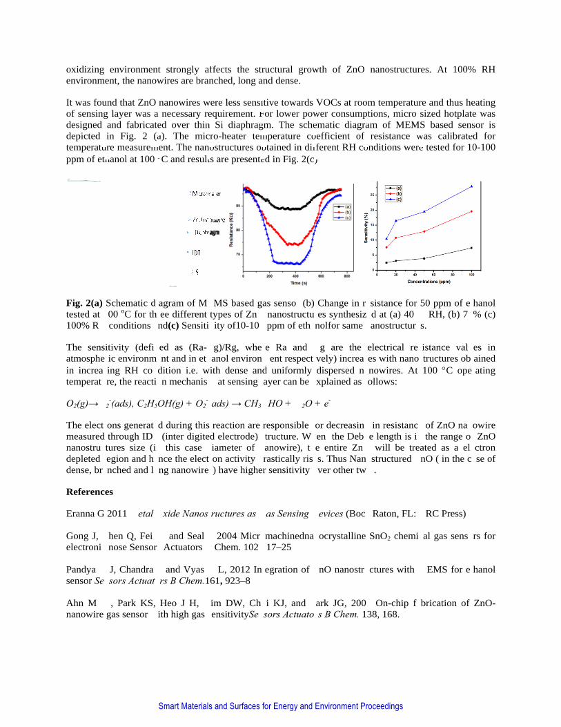
oxidizing environm
environmenent, the nanow
nt strongly afwires are bran
ffects the strnched, long a
ructural growand dense.
wth of ZnO nanostructurres. At 100%% RH
It was fouof sensingdesigned depicted temperatuppm of eth
Fig. 2(a) tested at 1100% RH
The sensatmospherin increastemperatu
O2(g)→O
The electrmeasured nanostrucdepleted rdense, bra
Referenc
Eranna G Gong J, Celectronic Pandya Hsensor Sen Ahn M Wnanowire
und that ZnO g layer was aand fabricatin Fig. 2 (a
ure measuremhanol at 100 °
Schematic di100 oC for thr
H conditions a
itivity (definric environmesing RH conure, the reactio
O2-(ads), C2H5
rons generatethrough IDE
ctures size (inregion and heanched and lo
es
2011 Metal O
Chen Q, Fei Wc nose Sensors
H J, Chandra nsors Actuato
W, Park KS, gas sensor w
nanowires wa necessary reed over thina). The mic
ment. The nano°C and result
iagram of MEree different
and(c) Sensitiv
ned as (Ra-Rent and in eth
ndition i.e. won mechanism
OH(g) + O2-(
ed during this E (inter digiten this case dence the electrong nanowires
Oxide Nanost
W and Seal Ss Actuators B
S and Vyas Aors B Chem.1
Heo J H, Kwith high gas s
were less sensiequirement. F
n Si diaphragro-heater temostructures obts are presente
itive towards For lower powgm. The schemperature cobtained in difed in Fig. 2(c)
VOCs at roower consumpematic diagraoefficient of fferent RH co)
m temperaturtions, micro am of MEM
resistance wonditions were
re and thus hesized hotplatS based sens
was calibratee tested for 1
eating e was sor is
ed for 0-100
EMS based gtypes of ZnOvity of10-100
Rg)/Rg, wherhanol environmith dense anm at sensing l
(ads) → CH3C
reaction are d electrode) s
diameter of nron activity ds) have highe
tructures as G
S 2004 MicroB Chem. 102 1
A L, 2012 Int61, 923–8
Kim DW, ChosensitivitySen
as sensor (b) O nanostructur0 ppm of etha
re Ra and Rment respectid uniformly layer can be e
CHO + H2O
responsible fstructure. Whnanowire), thdrastically riser sensitivity o
Gas Sensing D
omachinednan117–25
tegration of Z
oi KJ, and Pnsors Actuator
Change in reres synthesize
anolfor same n
Rg are the ively) increasdispersed na
explained as f
+ e-
for decreasinghen the Debyhe entire ZnOes. Thus Nanoover other two
Devices (Boca
nocrystalline
ZnO nanostru
Park JG, 2009rs B Chem. 1
esistance for ed at (a) 40 %nanostructure
50 ppm of et% RH, (b) 70es.
thanol 0% (c)
electrical resses with nanosanowires. At follows:
sistance valustructures obt100 °C oper
ues in tained rating
g in resistanceye length is inO will be treostructured Zo .
e of ZnO nann the range ofated as a ele
ZnO ( in the ca
nowire f ZnO ectron ase of
a Raton, FL: C
SnO2 chemic
uctures with M
9 On-chip fa38, 168.
CRC Press)
cal gas sensoors for
MEMS for etthanol
abrication of ZnO-
Smart Materials and Surfaces for Energy and Environment Proceedings
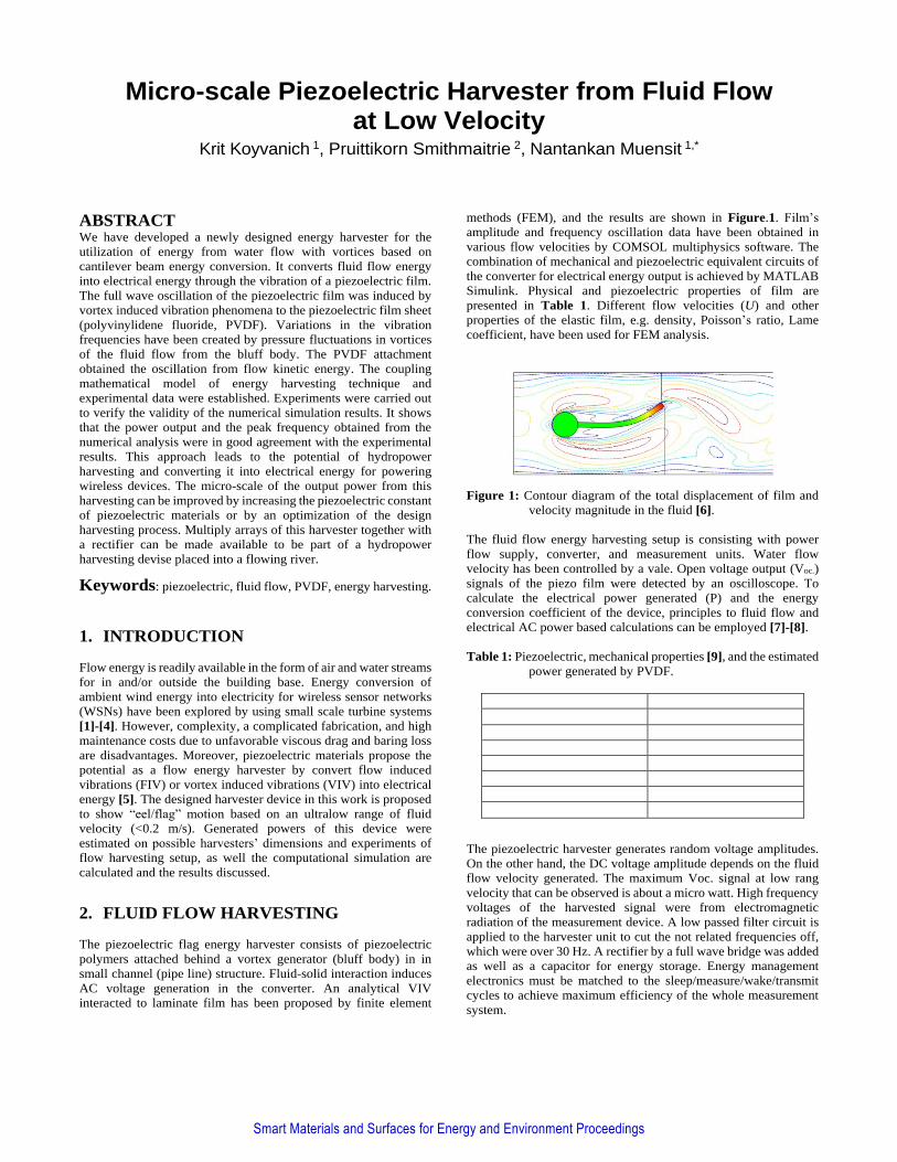
Micro-scale Piezoelectric Harvester from Fluid Flow at Low Velocity
Krit Koyvanich 1, Pruittikorn Smithmaitrie 2, Nantankan Muensit 1,*
ABSTRACT
We have developed a newly designed energy harvester for the
utilization of energy from water flow with vortices based on
cantilever beam energy conversion. It converts fluid flow energy
into electrical energy through the vibration of a piezoelectric film.
The full wave oscillation of the piezoelectric film was induced by
vortex induced vibration phenomena to the piezoelectric film sheet
(polyvinylidene fluoride, PVDF). Variations in the vibration
frequencies have been created by pressure fluctuations in vortices
of the fluid flow from the bluff body. The PVDF attachment
obtained the oscillation from flow kinetic energy. The coupling
mathematical model of energy harvesting technique and
experimental data were established. Experiments were carried out
to verify the validity of the numerical simulation results. It shows
that the power output and the peak frequency obtained from the
numerical analysis were in good agreement with the experimental
results. This approach leads to the potential of hydropower
harvesting and converting it into electrical energy for powering
wireless devices. The micro-scale of the output power from this
harvesting can be improved by increasing the piezoelectric constant
of piezoelectric materials or by an optimization of the design
harvesting process. Multiply arrays of this harvester together with
a rectifier can be made available to be part of a hydropower
harvesting devise placed into a flowing river.
Keywords: piezoelectric, fluid flow, PVDF, energy harvesting.
1. INTRODUCTION
Flow energy is readily available in the form of air and water streams
for in and/or outside the building base. Energy conversion of
ambient wind energy into electricity for wireless sensor networks
(WSNs) have been explored by using small scale turbine systems
[1]-[4]. However, complexity, a complicated fabrication, and high
maintenance costs due to unfavorable viscous drag and baring loss
are disadvantages. Moreover, piezoelectric materials propose the
potential as a flow energy harvester by convert flow induced
vibrations (FIV) or vortex induced vibrations (VIV) into electrical
energy [5]. The designed harvester device in this work is proposed
to show “eel/flag” motion based on an ultralow range of fluid
velocity (<0.2 m/s). Generated powers of this device were
estimated on possible harvesters’ dimensions and experiments of
flow harvesting setup, as well the computational simulation are
calculated and the results discussed.
2. FLUID FLOW HARVESTING
The piezoelectric flag energy harvester consists of piezoelectric
polymers attached behind a vortex generator (bluff body) in in
small channel (pipe line) structure. Fluid-solid interaction induces
AC voltage generation in the converter. An analytical VIV
interacted to laminate film has been proposed by finite element
methods (FEM), and the results are shown in Figure.1. Film’s
amplitude and frequency oscillation data have been obtained in
various flow velocities by COMSOL multiphysics software. The
combination of mechanical and piezoelectric equivalent circuits of
the converter for electrical energy output is achieved by MATLAB
Simulink. Physical and piezoelectric properties of film are
presented in Table 1. Different flow velocities (U) and other
properties of the elastic film, e.g. density, Poisson’s ratio, Lame
coefficient, have been used for FEM analysis.
Figure 1: Contour diagram of the total displacement of film and
velocity magnitude in the fluid [6].
The fluid flow energy harvesting setup is consisting with power
flow supply, converter, and measurement units. Water flow
velocity has been controlled by a vale. Open voltage output (Voc.)
signals of the piezo film were detected by an oscilloscope. To
calculate the electrical power generated (P) and the energy
conversion coefficient of the device, principles to fluid flow and
electrical AC power based calculations can be employed [7]-[8].
Table 1: Piezoelectric, mechanical properties [9], and the estimated
power generated by PVDF.
Young’s modulus (GPa) 6.9
r/o 12-13
d31 (pC/N) 23
d33 (pC/N) -33
k31 12%
k33 14%
Volume (µm3) 6400
P (µW) 1
The piezoelectric harvester generates random voltage amplitudes.
On the other hand, the DC voltage amplitude depends on the fluid
flow velocity generated. The maximum Voc. signal at low rang
velocity that can be observed is about a micro watt. High frequency
voltages of the harvested signal were from electromagnetic
radiation of the measurement device. A low passed filter circuit is
applied to the harvester unit to cut the not related frequencies off,
which were over 30 Hz. A rectifier by a full wave bridge was added
as well as a capacitor for energy storage. Energy management
electronics must be matched to the sleep/measure/wake/transmit
cycles to achieve maximum efficiency of the whole measurement
system.
Smart Materials and Surfaces for Energy and Environment Proceedings

3. RESULTS AND DISCUSSIONS
This work presents an energy harvester, i.e. a micro-generator,
utilizing fluid flow by using the piezoelectric principles. Although
experiments were not performed at resonance frequency, the device
can generate the fs oscillation of an ambient system reaching
resonance frequency by using a tailored fluid velocity of 6.8 m/s.
The Re number will be 5,000 and the flow can reach unsteady-
oscillating state in order to increase the output power. An outlook
of possible river flow and small channel energy harvesting
solutions for powering low power monitoring sensor nodes is
given. In view of this conclusion, future research will focus on the
developing of further physical factors as the distance to achieve
maximum vortex power from the harvester and testing this
experimentally in real river flow conditions. Power levels available
by using the considered harvesting solutions will also be
experimentally estimated as well as the optimization of the power
management electronics.
4. ACKNOWLEDGMENTS
Authors are thankful to the Center of Excellence in
Nanotechnology for Energy (CENE) and the Graduate School for
financial support and the Department of Physics and the
Department of Electrical Engineering for advice; all units are part
of Prince of Songkla University, HatYai Campus.
5. REFERENCES
[1] Priya, S., Myers, R., Vickers, M., and Kim, H. 2007. Small
scale windmill. Appl. Phys. Latt. 90, 054106 (Jan. 2007),
pp.1-3.
[2] Park, J.W., Jung, H.J., Jo, H., and Spencer, B.F. Jr.,
Feasibility Study of Micro-Wind Turbines for Powering
Wireless Sensors on a Cable-Stayed Bridge, Energ. 5, (Sep.
2012), 3450-3464. DOI:10.3390/en5093450.
[3] Azevedo, J.A.R., Santos, F.E.S., Energy harvesting from
wind and water for autonomous wireless sensor nodes, IET
Circuits Devices Syst. 6, 6, (Aug. 2012), pp.413-420.
DOI:10.1049/iet-cds.2011.0287.
[4] PRIYA, S., CHEN, C.T., FYE, D., and ZAHND, J.,
Piezoelectric Windmill: A Novel Solution to Remote
Sensing, Jpn. J. Appl. Phys. 44, 3 (Dec. 2004), pp. L104–
L107. DOI: 10.1143/JJAP.44.L104.
[5] Rao, K.M., and Manur, A.G., Modeling of Vortex Induced
Vibration based Hydrokinetic Energy Converter, IOSR-
JEEE, 6, 6 (Jul.-Aug. 2005), pp.26-31; e-ISSN: 2278-1676;
p-ISSN: 2320-3331.
[6] Turek, S., and Hron, J., Proposal for numerical
benchmarking of fluid-structure interaction between an
elastic object and laminar incompressible flow, Institute for
Applied Mathematics and Numerics, University of
Dortmund, Dortmund, Germany. pp. 246-260. Web
available:http://adhesion.ucd.ie/ccm/CCM_II_files/Hron%20
Turek%20Benchmark.pdf
[7] White F.M.; Fluid Mechanics (4th eds.), McGraw-Hill
international (eds.); 2003
[8] Cook-Chennault, K.A., Thambi, N., and Sastry, A.M.,
Powering MEMS portable devices—a review of non-
regenerative and regenerative power supply systems with
special emphasis on piezoelectric energy harvesting systems,
Smart Mater. Struct. 17, (June 2008), 043001, pp. 1-33.
DOI:10.1088/0964-1726/17/4/043001
[9] Piezo Film Sensors Technical Manual, Measurement
Specialties, Inc., P/N: 1005663-1, 1999. Web available:
http://www.https:/www.sparkfun.com/datasheets/Sen-
sors/Flex/MSI-techman.pdf
Smart Materials and Surfaces for Energy and Environment Proceedings

Effect of electron beam on thermal, morphological and antioxidant properties of kraft lignin
N.RajeswaraRao,1 T.Venkatappa Rao,1* SVS.Ramana Reddy,1 B.Sanjeeva Rao2
1National Institute of Technology, Warangal, INDIA 2Govt. Degree College, Mulugu, Warangal, INDIA
*Corresponding author Email: [email protected]
Abstract: Thermal, morphological and antioxidant
properties of lignin irradiated with electron beam of
doses 30, 60 and 90 kGy have been investigated by
ESR, FITR, DSC, SEM and Spectrophotometer
techniques. The absorption band at 1604cm-1 reveals
the presence of conjugated structures whose
concentration increases with the dose of irradiation.
Glass transition temperature of lignin decreased
abruptly at 90 kGy of dose and cracks were generated
in lignin granules on EB irradiation. Antioxidant
studies shows that the irradiated lignin with destructed
particles and high conjugation exhibit high antioxidant
activity compared to the unirradiated.
1. Introduction
Lignin, a natural polymer found in the cell walls of
plants along with the other two major components,
cellulose and hemicellulose. Lignin comprises 28% of
the mass of wood-like plants. In wood, lignin consists
of a family of phenyl-propane type polymers in a
variety of structural units. In addition, lignin has a
complex chemical functionality of carboxyl groups
and alcohols [1]. In fact, due to its non-toxic nature,
renewability and extreme versatility, lignin
applications have been increasing in industry. The
radiation induced modification of biopolymers is a
feasible method to produce material or to tailor their
usage. Electron beam (EB) irradiation is a promising
green tool in this respect and optimized/alternative
methods to utilize and to improve lignin as a precursor
in a cost effective manner. The radioactive
degradation of kraft lignin has been the subject of
numerous investigations.
Barca et al [2] have reported that phenolic
model compounds recognized as indigenous to the
lignin structure which possess significant antioxidant
property. Structures with conjugated double bonds in
propyl side chains have higher antioxidant activities
compared to structures with saturated side chains or
isolated double bonds. Lignin also contains ortho-
distributed phenolic groups. In addition, ortho-
methoxy groups might provide stabilization to the
incipient phenoxy radical formed by resonance
structures.
In the present study, electron beam irradiation of
different doses was applied to lignin. Under the
treatment from an electron beam, lignin compounds
are known to undergo several radical initiated
reactions such as aryl hydroxylation, fragmentation
and cleavage. These reactions leave the compound
open to interaction with number of resins systems
which have the capability to change the mechanical
properties and biodegradability of resulting
composite. In such cases it is necessarily important to
study the properties of lignin such as radical stabilities,
thermal properties and morphology on EB treatment
which can effect composite properties. Further, lignin
aromatic structures suggests that it is suited as a radical
scavenger in existing commodity thermoplastics. Also
there are limited number of papers dealing with EB
irradiation of lignin as a source for antioxidant
activity.
2. Material and Methods
Kraft lignin in the form of powder was purchased from
Sigma Aldrich, USA. Three lignin sample packets
were prepared for electron beam irradiation with
optimum radiation doses i.e. 30, 60 and 90 kGy. The
industrial electron beam accelerator is ILU-6 type,
pulse linear accelerator from Board of Radiation and
Isotope Technology, BARC, INDIA. In the present
studies, the dose rate chosen is 5 kGy/pass. Chemicals
like 1,1-diphenyl-2-picrylhydrazyl (DPPH),
Methanol, L-ascorbic acid, trichloroacetic acid (TCA)
and other reagents were purchased from HiMedia
Laboratories to study the radical scavenging activities.
ESR spectra were recorded on JES-FA200 ESR
spectrometer, JOEL at an operating frequency of 9.4
GHz (X-band). FTIR spectra of the sample pellet
prepared by adding KBr were recorded on Perkin
Elmer spectrometer. DSC measurements were
performed on a DSC-TA Q10 model calorimeter at a
heating rate of 20oC/min in flushing Nitrogen gas. The
X-ray diffractograms were recorded on Bruker D8
Advance XRD. The morphology of lignin was
examined under TESCAN VEGA 3 LMU with a
magnification of 750 and 1000. Lignin antioxidant
capacity was determined by using DPPH scavenging
activity and reducing power. The methods were
followed from Mir Gul et al [3] and Qi Lu et al [4] with
minor modifications.
Smart Materials and Surfaces for Energy and Environment Proceedings

3. Results and Discussion
Unirradiated lignin shows a weak ESR singlet with g-
value of 2.0035 and it is assigned due to poly-
conjugated radicals whereas the irradiated lignin
shows a strong singlet with increasing dose assigned
to two types of radicals (i) poly-conjugated radical (ii)
peroxy radical. Lignin contain phenols, alcohol,
glycosidic and acetal oxygen groups. When lignin is
irradiated with electron beam, dissociation of these
groups takes place and degradation occurs producing
primary radicals. Kuzina et al [5] have used D-band
ESR spectroscopy to resolve the singlets and detected
the existence of poly-conjugated radicals in lignin. In
the present studies, ESR spectrum of irradiated lignin
is a superposition of singlets arising due to the poly-
conjugated radicals and peroxy radicals. There is a
gradual increase in intensity of ESR signal with
radiation dose. ESR spectra are also recorded at RT,
333K, 363K, 413K and 453K temperatures shown in
Figure 1. As the temperature is increased, the radicals
gain thermal energy and begin to interact with
themselves or with other radicals. It is evident that the
doublet like structure appeared around 363K is
disappeared at 413K i.e. around glass transition
temperature of lignin. The decayed component is
assigned to peroxy radical. Since the poly-conjugated
radicals have high thermal stability, the singlet at
450K corresponds to poly-conjugated radicals.
Absorption spectra of lignin reflects the change in the
chemical structure induced on irradiation. The FTIR
studies confirm the enhancement in conjugation of
lignin on irradiation. These changes suggest that
cleavage of phenoxy groups on irradiation and
subsequently led to the formation of unsaturated
conjugated group. DSC thermograms shows a
negligible change in glass transition temperature (Tg)
but at a radiation dose of 90 kGy, the Tg decreased
abruptly. The decrease in Tg is assigned to a decrease
in molecular weight and plastification phenomena in
lignin which arise due to the intermolecular interaction
of hydroxyl groups. SEM micrographs shows
numerous pits on the cross-section surface of lignin
granule. When the lignin is treated with EB radiation,
cracks were developed on the surface of the cross-
section view of granule. The antioxidant activity of
lignin increased on EB irradiation was checked with
DPPH radical scavenging activity and reducing power
as shown in Figure 2.
4. Conclusion
Electron beam irradiation of kraft lignin induce both
physical and chemical changes. Cleavage of
glycosidic oxygen groups in lignin is occurred
producing poly-conjugated and peroxy radicals under
oxygenated conditions. Due to the chain cleavage,
glass transition temperature is found to decrease.
Electron beam irradiation also decreased particle size
with heavy damage of surface. Antioxidant properties
are also observed to increase due to irradiation of
lignin.
References: 1) Chuaqui CA, Rajagopal S, Kovacs A, Stepanik T.
Tetrahedron 1993, 49, 9689-9698.
2) Braca A, Sortino C, Politi M, Morelli I, Mendez J.
Journal of Ethnopharmacol 2002, 79, 379–381.
3) Gul ZM, Farhan A, Anand K, Qureshi A, Irfan G. BMC
Complementary and Alternative Medicine 2013, 13: 1-
12.
4) Qi L, Minghua Z, Yuangang Z, Wenjun L, Yang L, Ying
Z, Xiuhua Z, Xiunan Z, Xiaonan Z, Wengang L. Food
Chemistry 2012, 135, 63–67.
5) Kuzina SI, Brezgunov AY, Dubinskii AA, Mikhailov
AI. Radiation chemistry 2004, 38, 298-305.
Figure 1 ESR spectra of irradiated lignin at different
temperatures RT, 333K, 363K, 413K and 453K.
Figure 2 DPPH radical scavenging capacity of unirradiated
and irradiated lignin (A), Reducing power of unirradiated and irradiated lignin (B)
Smart Materials and Surfaces for Energy and Environment Proceedings

Facile growth of carbon nanotube electrode from electroplated Ni catalyst for supercapacitors
V. Yordsri,
1,2 W. Wongwiriyapan,
1,3,4* C. Thanachayanont
2
1College of Nanotechnology, King Mongkut’s Institute of Technology Ladkrabang, Chalongkrung Rd.,
Lardkrabang, Bangkok, Thailand 2National Metal and Materials Technology Center, 114 Thailand Science Park, Paholyothin Rd., Klong 1, Klong
Luang, Pathumthani, Thailand 3Nanotec-KMITL Center of Excellence on Nanoelectronic Device, Chalongkrung Rd., Ladkrabang, Bangkok,
Thailand 4Thailand Center of Excellence in Physics, CHE, Si Ayutthaya Rd., Bangkok, Thailand
Abstract: A facile growth of carbon nanotubes
(CNTs) was facilitated by the use of direct-current
plating technique for catalyst preparation. Ni
nanoparticles (NPs) were deposited on Cu sheet at
different applied voltages of 1.0, 1.5 and 2.0 V and
were subsequently used as catalyst for CNTs
synthesis by chemical vapor deposition (CVD)
method. Ni NPs size could be controlled by
electroplated voltage. A voltage of 1.5 V is the
optimum condition to deposit a uniform Ni NPs with
a narrow size distribution of 55±3 nm, resulting in
the synthesized CNTs with a uniform diameter of
approximately 60±5 nm with graphitic layers being
parallel to the CNTs axis. Ni NPs with a narrow size
and a uniform diameter is a key for uniform CNT
synthesis. Moreover, the CNTs synthesized from
electroplated Ni NPs shows the potential application
as pseudocapacitor.
Keywords: Electroplating, Carbon nanotube,
Chemical vapor deposition, Pseudocapacitor
Introduction
Carbon nanotube (CNT) shows a great
potential to apply in various applications to improve
device properties such as electronics devices, energy
storage devices and sensors. Chemical vapor
deposition (CVD) is one of the main methods for
CNT synthesis. Metal catalyst is an essential
ingredient for CVD approach (Lee et al., 2002). For
practical application, facile catalyst preparation is
strongly required. In this study, a facile growth of
CNTs was proposed by using direct-current (DC)
electroplating for Ni nanoparticles (NPs) preparation
and CNTs was synthesized by CVD using ethanol as
carbon source. Moreover, for potential application
demonstration, the supercapacitor based on the
synthesized CNTs were fabricated and its
electrochemical properties were characterized.
Experimental
The 4x20 mm2 Cu sheet (Nilaco
Corporation, Japan) and Ni ingot were connected as
anode and cathode, respectively. The commercial Ni
electroplating was used as electrolyte. Electroplating
temperature, time and distance between electrodes
were fixed at 45ºC, 5 min and 100 mm, respectively,
while the applied voltages were varied at 1.0, 1.5 and
2.0V. The CNT synthesis procedure is described as
follows. A quartz tube reactor was filled with Ar gas
at a flow rate of 500 sccm and the Ni catalyst-
electroplated Cu sheet was heated to 800ºC. Ethanol
(99.9%, Labscan) was vaporized and switched into
the quartz tube by Ar bubbling for 20 min for CNT
growth. Morphology of the electroplated Ni was
characterized by atomic force microscopy (AFM).
Morphology, diameter and crystallinity of the
synthesized CNTs were characterized by filed
emission scanning electron microscopy (FESEM) and
transmission electron microscopy (TEM). The
electrochemical measurements were carried out in a
three-electrode setup connected to an electrochemical
workstation (Metrohm AUTOLAB PGSTAT 302).
The synthesized CNT on Ni-electroplated Cu sheet
with an area of 4x10 mm2 was used as a working
electrode. Pt and Ag/AgCl electrodes were used as
counting and reference electrode, respectively. 1M
H2SO4 aqueous solution was used as the electrolyte
Results and discussion
Ni NPs could be formed by all electroplated
voltage conditions. The average size of Ni NPs
deposited at electroplated voltages of 1.0, 1.5 and 2.0
V were 120±14 nm, 55±3 nm and 103±12 nm,
respectively (data not shown). Thus, Ni NPs with a
controllable size can be achieved under the
controlled electroplating condition. Figures 1(a)−1(c)
show SEM images of CNTs synthesized from Ni NPs
deposited at electroplated voltages of 1.0, 1.5 and 2.0
V, respectively (hereinafter referred to as Ni1.0-
Smart Materials and Surfaces for Energy and Environment Proceedings

CNTs, Ni1.5-CNTs and Ni2.0-CNTs, respectively).
After CVD process, all Cu sheet surfaces were
wholly covered with a black powder by visual. All Ni
NPs could act as a catalsyt to synthesize tubular
shapes but different in morphologies and structures.
For Ni1.0-CNTs, the synthesized CNTs were tangled
in network while the Ni1.5-CNTs were straight with
high aspect ratio. For Ni2.0-CNTs, the synthesized
CNTs were curly and agglomerated in cluster
structure. From TEM observation, it was found that
graphitic layers of the Ni1.0-CNTs were angle to the
tube axis wall, while graphitic layers of the Ni1.5-
CNTs were parallel to the tube axis (data not shown).
For the preliminary test as supercapacitor
application, the Ni1.5-CNTs on Cu sheet was further
evaluated their electrochemical properties. Figure 2
shows the cyclic voltammetry (CV) curves of the
Ni1.5-CNTs in the potential range of -0.3−0.2 V at
different scan rates. Every CV curves show a pair of
redox current peaks, showing that faradic
pseudocapacitance is dominantly contributed to the
electrochemical properties (Li et al., 2013). With
increasing scan rate, the current increased and the
gap between redox peaks widened while the shape of
the CV curves were retained, indicating the redox
reversibility. This psesudocapacitive character may
arises from the residual Ni NPs used as catalyst for
CNTs synthesis. The specific capacitance calculated
from the CV curve at a scan rate of 5 mVs-1
is
approximately 53 Fg-1
. This preliminary results show
that the facile growth of CNTs from Ni NPs
deposited by DC electroplating method was
successful. The synthesized CNTs shows a potential
application as supercapacitor electrode. However,
further detailed works and optimization are needed
Conclusion
Novel synthesis of CNTs with simple and
low cost method was proposed by the use of
controllable electroplated Ni NPs as catalyst and the
use of ethanol as carbon source during CVD process.
The electroplated voltages directly affect the size of
Ni NPs, resulting in the morphology and structure of
CNTs. The graphitic layers of CNTs can be
selectively parallel to the tube axis with a narrow
tube diameter distribution of 60±5 nm. The
synthesized CNTs show a potential application as
supercapcitor with a specific capacitance of 53 Fg-1
at a scan rate of 5 mVs-1
. The optimization of Ni NPs
structure and the optimum amount of Ni NPs and
CNTs may improve the electrocapactive
performance.
Acknowledgements
We acknowledge support from the Thailand
Research Fund (DBG5580005) and from the
National Nanotechnology Center (NANOTEC),
NSTDA, Ministry of Science and Technology,
Thailand, through its program of Center of
Excellence Network and the Thailand Center of
Excellence in Physics (ThEP).
References: Lee, C.J., Park, J., Yu, J.A. (2002), Catalyst effect on
carbon nanotubes synthesized by thermal chemical vapor
deposition, Chem. Phys. Lett., 360, 250-255.
Li, H.B, Yu, M.H., Wang, F.X., et al. (2013), Amorphous
nickel hydroxide nanospheres with ultrahigh capacitance
and energy density as electrochemical pseudocapacitor
materials, Nature Communications, 4, 1-7.
Figure 1: SEM images of (a) Ni1.0-CNTs, (b) Ni1.5-CNTs and (c) Ni2.0-CNTs.
Figure 2: Cyclic voltammetry curves of Ni1.5-CNTs
with different scan rate
Smart Materials and Surfaces for Energy and Environment Proceedings

Immobilization of Urease Based on Adsorption in Eggshell
Membrane for Urea Biosensor Application Thanarat Suwanchaituch, Supranee Imthong, Kornvalai Panpae*
Department of Chemistry, Faculty of Science, King Mongkut’s University of Technology Thonburi,
KMUTT, Bangkok, Thailand
Abstract: In aqueous solutions, biomolecules such as
enzymes lose their catalytic activity rather rapidly,
because enzymes can suffer oxidation reactions or its
tertiary structure could be destroyed at the air/water
interface, hence making the use of enzyme and rea-
gents both expensive and complex. These problems
can be minimized considerably by enzyme immobiliza-
tion. By attachment to an inert support material, bio-
active molecules may be rendered insoluble, retaining
catalytic activity, thereby extending their useful life.
In view of the above necessity and advantages, since
the 1960s, an extensive variety of techniques have
been developed to immobilize biomolecules, including
adsorption, covalent attachment and entrapment in
various polymers ( Gupta et al; 2007). In general,
adsorption techniques are easy to perform, but the
bonding of the biomolecules is often weak and such
biocatalysts lack the degree of stabilization and easy
leakage from the matrix. A biosensor is an analytical
tool that comprises two essential components—an
immobilized biocomponent, in intimate contact with a
transducer that converts a biological signal into a
measurable electrical signal ( Turdean; 2011). Some
reports (D'Souza et al; 2012, Marzadori, et al; 1998)
on biosensors have been published using eggshell
membrane as a supporting matrix for immobilization
of enzymes such as D-amino oxidase, catalase, my-
rosinase, tyrosinase and glucose oxidase . The tech-
nique, which mostly used for immobilization of en-
zyme on eggshell membrane, involved adsorption
followed by cross-linking with glutaraldehyde. In this
study, a novel immobilization based on adsorption
method em ploying eggshell membrane from hard-
boiled eggs and fresh eggs as supporting matrice and
polyethyleneimine (PEI) as a carrier system was in-
vestigated using Jack bean urease as a model enzyme.
Eggshell membranes were studied differentiation of
morphology after urease immobilization by SEM.
They were studied the changes in IR spectra after
urease immobilization by FTIR. Immobilized mem-
brane was attached with a standard pH-electrode.
Biosensors of eggshell membrane from fresh egg and
hard- boiled egg response urea concentration range
from 7.5 mM to 200 mM. The response time of bio-
sensors was 300 s. Biosensors can be reused more
than 10 times with no significant decreasing of activi-
ty. The efficiency of urease immobilization on fresh
membrane is as well as that of boiled egg membrane.
Keywords: Potentiometric biosensor, eggshell mem-
brane, urease immobilization, urea biosensor.
1. Introduction
Enzymes have been utilized in a large number of
practical applications, particularly in biomedical and
bio- technological fields, through immobilization on a
variety of supports. These immobilized products were
intended for use in the construction of artificial organ
systems, biosensors or bioreactors. Immobilization is
advanta- geous because; (1) it extends the stability of
the bioactive species by protecting the active material
from deactivation; (2) enables repeated use; and (3) it
provides significant reduction in the operation costs.
Many methods exist for the immobilization of en-
zymes but usually one of four methods is used, physi-
cal adsorption, entrapment, co-polymerization, and
covalent attachment (Arica et al.; 2001). The meth-
ods and supports employed for enzyme immobiliza-
tion are chosen to ensure the highest retention of en-
zyme activity and its stability and durability. Urease
hydrolyses urea, yielding ammonia and carbonate. Immobilized urease has been widely used in biosen-
sors for diagnostic purposes, in the determination of
urea in biological fluids, in artificial kidney devices for
the removal of urea from blood for extracorporeal
detoxification, in enzyme reactor for the conversion
of urea present in fertilizer wastewater effluents or in
the food industry for removal of urea from beverages
and foods (Cevik et al; 2011). A variety of synthetic
as well as natural polymeric materials have been used
for the immobilization of enzymes for biosensor prep-
aration. Among these natural materials, especially of
proteinic origin, have shown promise uses. One of
these natural materials is the eggshell mem brane.
Some reports on biosensors have been published us-
ing eggshell membrane as a supporting matrix for
immobilization of enzymes such as D-amino oxidase,
catalase, myrosinase, tyrosinase and glucose oxidase
(D'Souza et al; 2012). The technique, which mostly
used for immobilization of enzyme on eggshell mem-
brane, involved adsorption followed by cross-linking
with glutaraldehyde.Glutaraldehyde has been used for
fixing the enzyme to the support and polyethyleneimine
(PEI) has been used for increasing the enezyme activity.
The study presented here used eggshell membrane as a
supporting matrix for urease immobilization. A novel
immobilization based on adsorption method em ploy-
ing eggshell membrane from hard-boiled eggs and
Smart Materials and Surfaces for Life Science

fresh eggs as supporting matrice and polyethylene-
imine (PEI) as a carrier system was investigated using
Jack bean urease as a model enzyme.
2. Experimental
2.1 Materials and reagents
Urea (enzyme grade), Jack bean urese (type III)
with specific activity of 35 units / mg protein was
obtained from Sigma. Urea (enzyme grade), polyeth-
yleneimine (PEI) were obtained from Sigma Chem.
Co. USA. All other chemicals used were of analytical
reagent grade.
2.2 Immobilization of urease on eggshell membrane
Fresh and hard-boiled eggs were broken and the
eggshell membrane was peeled off carefully from the
fresh eggshell. The membrane was washed with mil-
liQ water. Circular pieces (2 cm diameter) were cut
and were dried in an incubator at 35 °C for 1 h and
stored at 4 °C in the refrigerator. The membranes
were soaked for 2 h in 5% aqueous solution of PEI
(pH 7.0) at room temperature. The PEI-soaked mem-
branes were rinsed with milliQ water, air-dried for 1 h
and were stored in a petri dish at 4 °C. An aliquot of
100 μL of jack bean urease (100 units activity) was
adsorbed on each membrane. The membranes were
air dried at room temperature for 24 h. The immobi-
lized membranes were washed and immersed in buffer
(50 mM phosphate pH 7.0) and stored at 4 °C.
2.3 Membrane characterization 2.3.1 SEM
SEM observations were carried out on gold sput-
tered membrane samples using JEOL JSM-5410 LV
scanning electron microscope. Membrane samples for
SEM studies were prepared by soaking in isopropa-
nol, then in hexane for 3 h and subsequent vacuum
drying at 40 oC. The cross-sections of samples were
prepared by fracturing in liquid nitrogen.
2.3.2 FTIR study of enzyme immobilized membrane
Membranes were studied by FTIR spectra and
scanned in the range of 4000–400 cm−1 on Jasco
(Model FTIR-660 plus) FTIR Spectrometer. The
membranes were pressed directly onto the attenuated
reflectance with the sampling unit.
2.4 Calibration of biosensor using immobilized egg-
shell membrane
The standard solution of urea (0.5, 2.5, 5, 10, 25,
50 and 100 mM) was prepared in milliQ water. The
standard glass electrode was attached with urease
eggshell membrane. It was first stabilized with flow of
buffer as indicated by a stable baseline potential. Sub-
sequently, 1 mL solution of standard concentration of
urea was injected in the vessel and changes in poten-
tials in mVolts were recorded.
2.5 Activity assay
The membrane with the immobilized enzyme was
immersed in a 0.1 M solution of urea in 0.05 M sodi-
um phosphate buffer, pH 7.0, 37C. The membrane
(2 cm diameter) was attached to the tip of the stand-
ard glass electrode with the help of an O-ring and
then placed in the reaction vessel. The baseline poten-
tial of the sensor was achieved with flow of buffer
solution (50 mM phosphate pH 7.0). The solution
was stirred during the measurement on a magnetic
stirrer. The membrane electrode was allowed to stabi-
lize for 10 min before recording the reading. Between
measurements, the electrode membrane was washed
with buffer and used for the next reaction.
The relative activity was determined as the ratio
between the specific activity of a bound enzyme and
the specific activity of the free enzyme, multiplied by
100.
2.6 Determination of immobilized urease activity and
immobilized protein
The amount of protein bound to the modified mem-
branes was determined by the method of Lowry et al
(1951).
3. Results and discussion
3.1 SEM study of the urease immobilized eggshell
membrane
SEM study of immobilized eggshell membrane
showed a network- like structure without any aggre-
gation on the surface. Membrane consists of highly
cross-linked protein fibers and cavities and the obser-
vation was similar to the previous report (D'Souza et
al; 2012). Surface morphology of eggshell membrane
showed the fibers and cavities of the eggshell mem-
brane being occupied with PEI and urease enzyme
after immobilization (Fig.1). SEM micrographs indi-
cated that enzyme was successfully immobilized on
the surface of eggshell membrane using PEI.
3.2 FTIR study of urease immobilized eggshell mem-
brane
FTIR spectra of eggshell membrane are shown in
Figure 2. It is evident that the presence of amino
groups facilitates the immobilization of the enzyme by
a covalent linkage to glutaraldehyde-pretreated
membrane. As it can be seen (Fig. 2). It was observed
that four new peaks appeared at 3068, 1416, 1070
Smart Materials and Surfaces for Life Science

and 983 cm−1
after the PEI treatment on eggshell
membrane, which were corresponding to the=C-H
stretch of alkenes, -C-H bending of alkanes, C-N
stretch of aliphatic primary and secondary amines
(peptide) and C -H blending of primary and secondary
amines respectively. Results showed the occurrence
of PEI on egg shell membrane. After immobilization
of urease enzyme on eggshell membrane. Results
showed the presence enzyme on egg- shell membrane
as indicated in term of C-N amide bond in FTIR
study.The new groups increased the hydrophilicity of
the initial membrane.
Figure 1: SEM image of urease immobilized on egg-
shell membrane extracted from (A) fresh egg and (B)
hard-boiled egg.
Figure 2: FTIR study of eggshell membrane (A) Only
eggshell membrane, (B) Eggshell membrane treated
with PEI and (C) Urease immobilized on the PEI
treated eggshell membrane.
3.3 Activity and stability of immobilized urease and
immobilized protein
The general behaviors of urease immobilized onto
membranes under different conditions of immobiliza-
tion were studied. The activity of both free and im-
mobilized urease was determined by measuring the
amount of ammonia liberated from the urease-
catalyzed hydrolysis of urea per unit time :
The percentages of immobilization are summa-
rized compared with soluble enzyme.The highest ac-
tivity (53-54%) was measured for urease bound to
egg shell membranes at the optimum conditions:
0.01% enzyme solution, pH7.3 and 10% w/v PEI
time 2h, immobilization temperature 4 oC and immo-
bilization time 24h. The stability of urease was shown
by calculating the half-life of immobilized compared
with soluble urease (the results not shown). The half-
life of immobilized urease was approximately 37 days
when kept in 50 mM sodium phosphate buffer (pH
7.3) at 4˚C compared with a half-life of 28 days for
the soluble urease under identical conditions. The
higher stability of immobilized urease can be ascribed
to the protection of denaturation as a result of the
attachment of urase onto the eggshell membrane
cross-linked and adsorbed by PEI. Furthermore, the
storage stabilities showed good linearity with respect
to the activity
3.4. Response time, detection range and detection
limit
The biosensor prepared from urease immobilized
on egg shell membrane was used sucessfully for esti-
mation of urea samples. The calibration curve ob-
tained by plotting the potential difference (mV) across
the two leads of the separated glass electrode against
the concentration of urea is shown linearly in Figure 3
and the response time with the present experiments
(0.01 M urea at 7.3) is shown in Figure 4.
Figure 3: Calibration of the biosensor using immobi-
lized eggshell membrane.
A
B
C
Smart Materials and Surfaces for Life Science

Figure 4: Response time of enzymatic activity of
urease eggshell
The response time observed in the present study is
300 s comparable with those reported for other urea
biosensor (Srivastava et al.,2001; Schitogullari et al;
2002). Several parameters move evaluated to ascer-
tain the optimum performance of the base line, slope
of the calibration curve and reliability of the biosen-
sor. The detection limit in our case is approximately
7.0 mM. At different time intervals, variation in elec-
trode potential was monitored using 0.01M urea solu-
tion. A little loss of activity was observed over of 4-7
weeks and the reproducibility of the urea assay for the
serum samples obtained from our biosensor was ex-
pected to be very good compared with other reports
(Cevik et al; 2011, D'Souza et al; 2012, Magalhães et
al;1998).
4. Conclusion
Present communication describes a much simpler
method of immobilization of urease. Eggshell mem-
branes both from fresh egg and hard-boiled egg can
be used for the immobilization of enzymes through
adsorption for biosensor application. Biosensor exhib-
ited sigmoidal responses for the urea concentration
range from 7.5 to 200 mM. The estimated response
time of the biosensor was 300 s. A single membrane
was reused not less than 10 cycles of the urea hydrol-
ysis reaction. The immobilized membranes were sta-
ble for 2 months when stored in buffer at 4OC.
References:
Arica, MY.,Kacar, Y., Egene, A., Denizil, A.(2001),
Reversible immobilization of lipase on phenylalanine
containing hydrogel membranes, Process Biochem.,
36, 847-854.
Cevik, E., Senel, M., Abasiyanik, M.(2011), Immobi-
lization of urease on copper chelated EC-Tri beads
and reversible adsorption, Afri. J Biotechnol., 10,
6590-6597.
D'Souza, S.F., Kumar, J., Jha, S.K., Kubal, B.S.
(2012), Immobilization of the urease on eggshell
membrane and its application in biosensor, Mater.
Sci. Eng.C, 33, 850-854.
Gupta, R., Chaudhury, N.K. (2007), Entrapment of
biomolecules in sol-gel matrix for applications in bio-
sensors: Problems and future prospects, Biosens. Bi-
oelectron., 22, 2387-2399.
Lowry, O.H., Rosebrough, N.J. Farr, A.L., Randall, R.J
(1951). Protein measurement with the Folin phenol
reagent. J. Biol.Chem.,193, 265-275.
Magalhães, J.M.C.S., Machado, A.A.S.C.(1998),
Urea potentiometric biosensor based on urease im-
mobilized on chitosan membranes. Talanta, 47, 183-
191.
Srivastava, P.K., Kayastha, A.M., Srinivasan, F.S
(2001), Characterization of gelatin-immobilized pi-
geonpea urease and preparation of a new urea biosen-
sor. Biotechnol. Appl. Biochem. , 34, 55-62.
Sehitogullari, A., Uslan, A.H. (2002), Preparation of
a potentiometric immobilized urease electrode and
urea determination in serum, Talanta. 57, 1039-
1044.
Turdean, G.L. (2011), Design and development of
biosensors for the detection of heavy metal toxicity,
Int. J. Electrochem., 2011, Article ID 343125, 15
pages.
Smart Materials and Surfaces for Life Science

Needle-less Jet Injection System with Multi-Pore Nozzle for Viscous Drug Delivery Applications
Y. C. Jo,1* H. K. Hong,1 Y. S. Choi1, H. S. Kim2
1Korea Electronics Technology Institute, Medical IT Convergence Research Center, SeongNam-Si, South Korea 2Korea Electronics Technology Institute, Contents Research Center, SeongNam-Si, South Korea
Abstract: Jet injection is an important needle-free drug delivery method for insulin and vaccines[1-3]. Jet injections employ a high speed jet to puncture the skin and deliver drugs without the use of a needle. Although jet injections have been used for tens of years and continue to be researched for new applica-tions. Needle-free jet injection constitute an im-portant method of drug delivery, especially for beau-ty treatment. An experimental study was performed using a newly developed air-powered needle-free jet injector(Figure 1) to investigate the relationship be-tween nozzle pore variation and delivered viscous liquid drug volume. The most important injector fuction for beauty treatment are the penetration depth and diffusion area which is related with jet velocity and nozzle pore number. The driver pressure of the air cylinder considered in this work ranged from 6 to 10 bar provided by an air compressor fitted with a precision regulator. Individual nozzle and pressure combinations were tested a minimum of ten times in order to ensure consistent and reliable results. Devel-oped injector in this work is the first needle-free jet injector prototype with multi-pore nozzle for viscous drug delivery upto 12cps, 1% Hyaluronic Acid(HA) solution. The proposed injector has three types of nozzle structure, such as single pore, 4 pores array and 9 pores array nozzles(Figure 2). Experimental studies showed that the penetration depth and diffu-sion of drug into skin continue to decrease as the nozzle pore number increase(Figure 3, Figure 4). Keywords: Needle-free, Jet injector, Drug delivery, Skin, High viscosity, Beauty treatment
Figure 1: A New needle-free jet injector developed in these work. The injector is driven by a air com-pressor. The nozzle is made of clear thermoplastics.
(a) (b) (c)
Figure 2: Design models of the injector nozzles of the proposed jet injector used in these experiments. Each nozzle has different pore number. (a) single pore, (b) 4 pores array (c) 9 pores array
Figure 3: Sample pictures showing the jet penetra-tion generated by the air-powered injector with three different nozzle configurations(9, 4 and single pore) into the 5% gelatin block. All of the pore diameter was 100 um in common and 1% Hyaluronic Ac-id(HA) solution was used for this experiments
(a) (b) (c)
Figure 4: Guinea pig skin test results of the proposed device using designed nozzle with various pore num-ber, (a) 1 pore, (b) 4 pores array (c) 9 pores array
Acknowledgements This work was supported by the Korean Ministry of Trade, Industry & Energy and KEIT under contract No. 10044186
References: Portaro, R., Dick Ng, Hoi. (2013) Experimental anal-ysis of the performance of an air-powered needle-free liquid jet injector, IEEE EMBS. Baxter, J., Mitragotri, S.(2005), Jet-induced skin puncture and its impact on needle-free jet injections : Experimental studies and a predictive model, Int. J. Controlled Release, 106, 361-373. Baxter, J., Mitragotri, S.(2005), Needle-free jet injec-tions : dependence of jet penetration and dispersion in the skin on jet power, Int. J. Controlled Release., 97, 527-535.
Smart Materials and Surfaces for Life Science
