smart vehiclesneed smart memory architectures
TRANSCRIPT

SMART VEHICLES NEED SMART MEMORY ARCHITECTURESTHE NEED FOR EXECUTE-IN-PLACE (XIP)
Donnie Garcia – NXP Semiconductors, Product Marketing Manager for Wireless MCUsJohnny Chien – ISSI, Product Marketing Manager - Flash
How vehicles are becoming smart and what it means for memory architectures.

2 www.nxp.com
INTRODUCTIONFor years now, vehicles have adopted electronic components to become cleaner, safer, and more user-friendly. They are now made smarter by the addition of semiconductor components to sense, compute, and wirelessly connect. Microcontrollers (MCU) and microprocessors (MPU) aimed for transportation purposes that lean on specialized software are not easily portable across multiple computer chips, which limits the semiconductor components that can be used within vehicle electronics. This is one reason why planning for memory extensibility by design is desirable.
External MemorySemiconductor (DDR/ PSRAM,
NOR Flash)
MCU or MPU Semiconductor
System
Bus M
atrix
SRAM
ROM
Other BusFollowers
Internal Memory(On chip RAM,
Flash)
MCU or MPU Semiconductor
System
Bus M
atrix
CPU
Other BusLeaders
SRAM
ROM
Mem
ory Bus I/O
Other BusFollowers
OPEN ARCHITECHTURE CLOSED ARCHITECHTURE
ARCHITECTURES BLOCK DIAGRAM
CPU
Other BusLeaders
Both MCUs and MPUs operate by executing machine code stored in a memory that the central processing unit (CPU) must access. The way a particular processor is architected to execute software from memory can be classified into two categories: closed architecture and open architecture. Usually, the software runs only from memory built into the system-on-chip for closed architecture devices. The most simple and constrained embedded devices rely on MCUs built with an integrated non-volatile memory (NVM) for software. In contrast, open architecture devices allow for memory expansion using external components. The predominant memory architecture for microprocessors (MPU) is open architecture, and for the microcontroller, memory integration is the typical configuration with a closed architecture. Over the last few years though, more hybrid options have been introduced into the market including NXP’s i.MX RT crossover MCU series.
There are volatile and non-volatile options for external memory. An example of volatile memory is DRAM, used in personal computers or smartphones. Examples of non-volatile memory types are NAND flash and NOR flash. NOR flash uniquely allows for fast and random accesses necessary to run software. NOR flash provides an NVM option for open architecture designs due to its robustness, energy profile, and reliability. When an MCU or MPU uses external flash for software execution, the term of art associated with the software execution is Execute in Place, also known as XiP. An MCU or MPU that supports XiP includes internal mechanisms to fetch machine code from the external NOR flash device and execute software.
Figure 1. Closed Architecture vs Open Architecture
3www.nxp.com
HISTORY OF MEMORY ARCHITECTURESThe closed architecture running code from an integrated NVM is not a new concept. The first MCUs introduced in the market were based on a closed architecture executing software from an NVM implemented in a read-only memory (ROM) while the embedded read or write system memory (RAM) was used for storing variables and temporary data.
The XiP for open architectures became most known when parallel NOR flash was popularized. The closed architecture with internal RAM and flash is still used today, but limited mainly to embedded systems with smaller flash sizes. Commonly, open architecture becomes optimal for high-performance systems as flash memories cannot physically follow the same technology as the newest CPUs in a cost-effective manner.
For applications tending to limit power consumption (such as cell phones), running massive amounts of code out of DRAM leads to inefficiency. Therefore, external parallel NOR flash devices were used in the early days of cell phone design because DRAM tends to consume more power as it needs to be periodically refreshed. Moreover, NOR flash is a robust form of storage; collecting and executing code out of NOR flash implies that a smaller density of DRAM (cellular RAM or PSRAM for cell phones in its early days) was required, further reducing the total system cost.
Another key factor to consider is boot up time: transferring large amounts of code from NVM to DRAM and executing the code in DRAM requires a longer time to start. XiP significantly reduces booting time compared to copying code to DRAM for specific operations, like PCI-e which requires at least 100ms or less to boot up. With XiP, critical system functions can be directly executed from external memory, without spending the time transferring code to DRAM.
XiP from NOR flash became commonplace in the general embedded open architecture system by introducing a multi-lane (quad or octal) serial interface. The serial NOR flash represents significant pin savings over parallel NOR flash, remarkably reducing the controller’s pin count, which translates into lower packaging costs. In addition, the quad-lane serial flash can transfer data four times faster than a single-lane at the same clock frequency and up to 8 times faster in octal-lane flash. As a result, serial NOR flash has gained momentum among XiP open architectures in general embedded systems, primarily due to power and cost savings, coupled with a reduction of bootup times.

4 www.nxp.com
SERIAL NOR FLASH XIP IN AUTOMOTIVEEngineers are extending the traditional use of flash memory as data storage into applications that address the smart vehicles’ needs. Driving these requirements are trends associated to connectivity and edge intelligence.
Today’s smart vehicles require a host of new capabilities which incluede LTE, Wi-Fi cameras, and Bluetooth-assisted access control. The evolution of smart vehicles couples tightly with opportunities enabling wireless connectivity. Standardized protocols for LTE, Wi-Fi, and other wireless connectivity options costs memory requirements and space for code.
Simultaneously with connectivity, there are other massive code size needs related to edge intelligence. Enhanced human-machine interfaces (HMI) and advanced machine learning through neural networks require large data arrays that must be quickly accessed. These necessities match closely to the advantages of both open architectures and serial NOR flash devices.
This paper explores why XiP is pursued in the Automotive industry and the numerous benefits it has on the vehicle architecture.
Figure 2. Connectivity and Telematics

5www.nxp.com
SMART VEHICLES: RICH USER INTERFACES AND CONNECTIVITY
New capabilities such as intelligent car access and assisted driving in the smart vehicle are the driving forces behind XiP. Upon taking a closer look we can see how each new application contributes to the demand for XiP capabilities. In addition, there are system integration requirements for continuous software improvements, connectivity, and security for many application cases.1 To support constant software improvements, embedded systems built with the option of XiP allow for the memory requirements to grow. Furthermore, system memory is often up-sized to allow robust firmware updates and often times it is doubled to allow a backup or fallback image.
Connectivity implementations are increasing the number and types of wireless interfaces that the smart vehicle must support. First, there is the user experience vector within the vehicle, connecting drivers and passengers to Wi-Fi and Bluetooth as mobile phones become a central component in our day-to-day living. The second vector relates to services offered by the vehicle through telematics as the vehicle itself embeds LTE modems and links them directly to online monitoring and services, requiring software stacks that take up significant code space.2
Finally, there are stringent security concerns traversing all the other integration requirements, as it has to be considered across several aspects of the embedded design. Current cryptographic algorithms are increasing code size and placing additional demands on the embedded systems. Even though hardware-based cryptography has come a long way over the last years, protocols involved in establishing secure connections are still demanded, together with steps and procedures that must apply to assure reliability. For both, the case of supporting fully software-based cryptography and security algorithms or hardware-accelerated require additional code space. These integration requirements call for an increased need for memory expansion through open architectures with options, such as XiP.
From the software perspective, supporting continuous improvements requires an approach with dependencies around open-source community-based software components. Open source is essential for graphics libraries, connectivity, and security stacks. Their attributes emphasize on working on diverse platforms rather than size optimizations, leading again to a demand for memory expansion. Together with software design choices that rely on open source, there is the latent need to work well with ecosystems provided by the major smart phone operating system providers.
ADVANTAGES OF OPEN ARCHITECTURE
Whether for adding connectivity or addressing machine learning challenges, there is no denying that memory expansion is a common need across embedded designs. Memory can be added internally to a device as an alternative to external memory with XiP functionality, so the choice of memory architecture for the MCU/MPU must be explored.
So, what makes open architecture with XiP more attractive? From an embedded system designer perspective, the most crucial aspect of XiP is the associated scalability because external memory options can scale in performance and integration, offering a broad range of use cases addressed with the same processor. Besides, only the external memory device must be changed if higher memory or faster memory is required –instead of replacing the main MCU or MPU.
Many aspects of the hardware and software design are leveraged as product requirements change, in contrast with closed architectures when choosing to scale external memory. For instance, manufacturers can leverage the common external serial NOR flash PCB footprints to offer an easy upgrade path from Mbits up to the Gbit range for the latest memories when producing multiple product skews or adding new features, ensuring faster time to market, as well as lowering development costs.

6 www.nxp.com
Additionally, the external serial NVM alternatives in the market can be optimized for wafer capabilities, leading to a lower cost-per-bit of memory than internal memory options. In other words, systems that depend on XiP will be more affordable than processors that integrate large amounts of memory. Also, the cost-effectiveness increases when the system requires external NVM as many designs rely on serial NOR flash for data storage. Therefore, taking advantage of XiP in such a system represents the added system cost for code storage only when the bigger memory is needed to support the code size requirements. In short: there is no added cost due to PCB design or power management design as the serial NOR flash is already in the system.
The capabilities related to quality and robustness sum a lot of value together with the cost benefits of optimized technology that serial NOR flash brings. The serial NOR flash products typically offer wide temperature ranges, long data retention, and plentiful write-erase cycles. Also, serial NOR flash devices are manufactured on larger geometries than today’s processors. This allows NVM such as serial NOR flash to be used in harsh environments as
those required for automotive designs. As the processor is generally pushing the limits of silicon wafer design, it would not be able to integrate the NVM and keep all same attributes as offered by the specialized serial NOR flash devices.
There is a trend for processor architecture and performance that contributes to the adoption of XiP along with cost, robustness, and system scalability. Over the last years, industry-standard CPUs (such as those provided by Arm®) have enhanced their architectures to work better with cache-based systems, a relevant aspect of XiP. Besides, as processors are integrated into smaller manufacturing processes, their associated operation frequencies are being boosted to gigahertz speeds; cache-based architectures and high CPU speeds mitigate latencies introduced by serializing memory interfaces. As a result, memory access times are no longer a gating factor for an embedded system’s performance. Thus, serial NOR flash and XiP provide a path for the right mix of energy efficiency and performance needed for today’s embedded systems.
High Performance & Rich Interfaces Power Efficient & State Retention
Key Manager
Memory MappedCyrpto. Engine
Secure Storageand Tamper
1 GHzArm® Cortex®-M7
DMA DMA
System RAMwith ECC
Quad/Octal SPI interface
External Memory (Serial NOR Flash)
2xUSB 2.0 with PHY
2x Gb Ethernet (AVB, TSN)
10/100 Ethernet
MultimediaInputs
SerialPeripherals
VIDEOMUX
Timers andSpeed Sensors
2D GPU and 2D Accelerator
Analog(ADC, DAC)
Key Pad
MultmediaOutputs
Memory Interfaceswith Encrypted
Execution
EdgeLock 400A HW ROOT of TRUST
& Cryptography
2x, FlexIO
400 MHzArm® Cortex®-M4
I.MX RT1170 SUBSYST BLOCK DIAGRAM
Figure 3. Example Processor Architecture

7www.nxp.com
REASONS FOR CHOOSING NOR FLASHThe NOR flash is a robust and reliable storage with fast READ speeds and random-access capability, making it ideal for code storage and execution –specifically suitable for XiP. In the latest years, the logic process nodes shrank, but the flash process node did not decrease at the same rate: the embedded flash memory is hard to achieve beyond specific process nodes gated by the logic process. Since systems become more complex, both the code size increases and the need for larger code storage fueled the demand for flash memories to be external devices, resulting in fast adopting open architecture memory subsystems. The need for embedded system performance and code space is driven by the fact that today’s vehicles must integrate a staggering amount of functionality in the form of lines of code.[3] As illustrated by the prior graphic, there are actually more lines of code in the vehicle than aircraft, space craft, and even operating systems. This trend is apparent in the automobile, for industrial applications and others. This contributes to the need for the advancements in serial NOR flash capabilities and processors.
As a result, the need for an external NOR flash with a low pin count has risen –in which serial NOR flash became the natural default. Meanwhile, serial NOR has progressed from single-lane read to multi-lane read capabilities such as quad (4-lane) and octal (8-lane). This performance upgrade significantly enables XiP and its benefits: power and costs savings in addition to boot time improvement.
Today’s Vehicle contains >200 million lines of code
MODERN HIGH END CAR
LARGE HADRON COLLIDER
MARS CURIOSITY ROVER
HUBBLE SCAPE TELESCOPE
SPACE SHUTTLE SOURCE: CHOICE.COM.AU
KERNAL 2.6.0
787
Figure 4. Lines of code comparison with a modern vehicle
The car today contains more software than any other embedded system and most computer applications.

8 www.nxp.com
While open architecture calls for added security requirements, most automotive applications expect an additional layer of reliability and performance. Integrated Silicon Solution Inc. (ISSI) offers serial NOR flash families with added error correction code, AX mode, and security –optimizing flash access instructions and features. Their IS25 family of serial NOR flash devices provide a practical and viable solution to address those requirements.6 Note not all products have every feature supported. Contact [email protected] for more information.
Error correction code (ECC)
ISSI offers serial NOR flash devices with inline ECC capability that makes them backward compatible with standard memory –dramatically enhancing data robustness and quality, simplifying system-level design, saving power, and reducing the memory footprint on the board. The added ECC capability makes it ideal for high-reliability applications, especially the safety-critical applications in the automotive segment, helping to achieve the required functional safety defined by ISO 26262.
AX Read Mode
ISSI serial NOR flash devices offer AX read and AutoBoot modes for reading the data from the flash. The two are used for fast execution, requiring only an address to output data for random access. During power-on, the AX read mode cannot be directly accessed. Instead, the AutoBoot mode enables boot code to be sequentially read as it does not require a starting address or a read command. Starting address can be omitted by assigning a preselected address through a register setting. AX read mode operation is enabled by applying mode bits during the dummy period. Mode bits consist of 8 bits (M7 to M0). Enabling the AX read operation where subsequent read execution skips the command code when M[7:4]=1010(Ah) and M[3:0]=X (where X is don’t care) and the flash device exits the AX read operation when the mode bits are different from AXh. Both AutoBoot mode and AX read mode are designed to enhance the performance of Open Architecture memory subsystems.7
Figure 5. ISSI SPI flash for automotive

9www.nxp.com
Security and Protection1
ISSI addresses system vulnerabilities by utilizing key security features built into the QSPI/xSPI flash devices as the demand for secure flash solutions continue to expand in order to keep pace with the latest sophisticated hacking techniques. Their key security features are:
• BGA package: protecting the device from malicious probing by unwanted users. The BGA package’s balls are contained on the bottom of the device and soldered directly to the PCB. Traces to these balls can be embedded throughout a multi-layered PCB to prevent unwanted access. ISSI offers two types of 24-ball TFBGA packages to support SPI NOR devices: a 4x6 ball and a 5x5 ball array.
• Hardware write-protect: providing dedicated WP# pin in all of ISSI’s SPI flash for USON, WSON, SOIC, and BGA packages. The WP# pin protects the Status Register from being written. The Status Register bits contain controls for Quad Enable, Block Protection, and the WriteEnable Latch.
• Unique ID: using a 128-bit serial number implemented by ISSI to verify component authenticity, which cannot be changed but could be used with other critical system components such as microprocessors to reduce the threat of component swapping.
• OTP Area: allowing system designers to implement a hash type of algorithm on the memory array to generate an original value that can be stored in the One Time Programmable area (OTP) to verify code authenticity. The system uses the same algorithm to re-compute this value and compares it to the original value stored in OTP. If these values mismatch, the system could be compromised, requiring a follow-up action until problem resolution.
• Block protection: preventing accidental or malicious programming and erases through user-selectable locking blocks. These areas are temporarily locked and prevent unauthorized changes to the device.
• Advanced Sector Protection (ASP): allowing individual sector locking, which can be controlled by volatile register bits (dynamic protection bits) or non-volatile register bits (persistent protection bits). The Gang Sector/Block lock and unlock instructions provide a quick method to clear or set all Dynamic Protection Bits (DYB) bits at once. A 64-bit one-time programmable password can further protect the Persistent Protection Bits (PPB) changes.
• Replay Protection Monotonic Counter (RPMC): providing a building block for extra security, adding incremental monotonic counting to code and data storage in boot memory, preserving the uniqueness while helping to make systems more resistant to both rollbacks and replay attacks.
1 Not all products have every feature supported. Please contact [email protected] for more information
10 www.nxp.com
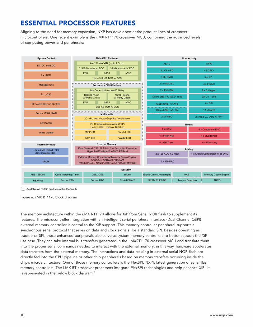
ESSENTIAL PROCESSOR FEATURESAligning to the need for memory expansion, NXP has developed entire product lines of crossover microcontrollers. One recent example is the i.MX RT1170 crossover MCU, combining the advanced levels of computing power and peripherals:
The memory architecture within the i.MX RT1170 allows for XiP from Serial NOR flash to supplement its features. The microcontroller integration with an intelligent serial peripheral interface (Dual Channel QSPI) external memory controller is central to the XiP support. This memory controller peripheral supports a synchronous serial protocol that relies on data and clock signals like a standard SPI. Besides operating as traditional SPI, these enhanced peripherals also serve as system memory controllers to better support the XiP use case. They can take internal bus transfers generated in the i.MXRT1170 crossover MCU and translate them into the proper serial commands needed to interact with the external memory; in this way, hardware accelerates data transfers from the external memory. The instructions and data residing in external serial NOR flash are directly fed into the CPU pipeline or other chip peripherals based on memory transfers occurring inside the chip’s microarchitecture. One of those memory controllers is the FlexSPI, NXP’s latest generation of serial flash memory controllers. The i.MX RT crossover processors integrate FlexSPI technologies and help enhance XiP –it is represented in the below block diagram.7
Figure 6. i.MX RT1170 block diagram
Timers
i.MX RT1170 CROSSOVER MCU FAMILY BLOCK DIAGRAM
2D GPU with Vector Graphics Acceleration
Parallel LCD
Parallel CSI
MIPI DSI
MIPI® CSI
Dual Channel QSPI FLASH x2 w/ Encrypted ExecutionHyperRAM™/HyperFLASH™/PSRAM
2D Graphics Acceleration (PXP)Resize, CSC, Overlay, Rotation
External Memory Controller w/ Memory Crypto Engine 8/16/32-bit SDRAM/LPSDRAM
8/16-bit Parallel NAND/NOR Flash/FPGA/SRAM/8080
Arm® Cortex®-M7 (up to 1 GHz)
2 x eMMC/SD
8-ch. DMIC
10/100 ENET w/ IEEE® 1588
1Gbps ENET w/ AVB
1Gbps ENET w/ TSN
2 x EMVSIM
3 x CAN-FD
2 x FlexIO
Up to 512 KB TCM w/ ECC
32 KB I-cache w/ ECC32 KB D-cache w/ ECC
FPU MPU NVIC
4 x Watchdog6 x GP Timer
4 x Quadrature ENC
4 x QuadTimer4 x FlexPWM
1 x EWM
Up to 2MB SRAM Total(Configurable ECC)
ROM
AES-128/256 Code Watchdog Timer
Secure RAM
Main CPU Platform
Arm Cortex-M4 (up to 400 MHz)
256 KB TCM w/ ECC
16KB I-cachew/ Parity Check
16KB D-cachew/ Parity Check
FPU MPU NVIC
Secondary CPU Platform
Multimedia
Internal Memory
Analog
External Memory
Security
System Control Connectivity
ASRC
2 x 12b ADC 4.2 Msps 4 x Analog Comparator w/ 8b DAC
1 x 12b DAC
Available on certain products within the family
PLL, OSC
Resource Domain Control
2 x eDMA
Message Unit
Semaphore
DC-DC and LDO
Temp Monitor
Secure JTAG, SWD
RSA4096
eFuse Elliptic Curve Cryptography HABDES/3DES Memory Crypto Engine
TRNGSHA-1/SHA-2Secure RTC Tamper DetectionSRAM PUF/UDF
12 x UART
4 x I2S/SAI
2 x USB 2.0 OTG w/ PHY
GPIO
HS GPIO
6 x I2C
8 x 8 Keypad
6 x SPI
S/PDIF Tx/Rx

11www.nxp.com
The 64bit AHB bus is the interface to the system bus, which will come from a CPU or other on-chip masters (like an LCD controller).
The IPS BUS is an external interface but allows the software to directly send commands to the NOR flash device through the FlexSPI register model. This interface is also used to initialize and configure the external serial flash, as it can be used to initiate the process of sending commands.
Connected to the AHB_CTL block, transmit (TX) and receive (RX) buffers prefetch data when reading the external memory to improve latency and overall compute performance for the XiP operation.
The sequence control block (SEQ_CTL) is a large look-up table holding preset instructions for different serial flash operations such as read, erase and program. The SEQ_CTL links access from the 64-bit AHB bus to the read command sequence, which is sent to the external serial flash. Not every flash will have the same command set or I/O interface.
Figure 7. FlexSPI BLOCK DIAGRAM
FLEXSPI BLOCK DIAGRAM
AHB_CTL
AHB_CTL
RX_FIFOASYNC
CDC_SYNCH(Clock domain
Cross)
TX_FIFOASYNC
AHB_CTL SEQ_CTL(Sequence) IO_CTL
SPI BusFA Port
Data
DataData
Data Data
ARB_CMD SEQ_CMD
Data
Data
Data
SPI BusFB Port
AHB_CMD
IP_CMD
IP_RX_FIFOIP_RX_CTL
(arbitrator)
AHB_RX_BUF
AHB_TX_BUF
AHB BUS 64 bit
IPS BUS 32 bit IP_RX_FIFO
IP_RX_CTL
The sequence control engine is programmable for adjusting the SPI transfers based on the command set defined by the serial flash, allowing processors (like the i.MX RT1170) to interface with a broad range of external flash types and capabilities. Furthermore, this flexibility enables the crossover processor to utilize flash attributes that play a critical role in supporting the most capable XiP embedded systems.
CONCLUSIONConsumer demands for innovative and helpful features continuously change in the automotive space and the whole electronic world, creating new trends for engineers to work with. Richer human-machine interactions influence all aspects of embedded design.
As vehicles become smarter and demand more resources, considering memory architecture and planning for scalability is essential to reliable, successful, and robust systems. With the open architecture and Execute-In-Place (XiP) operation, embedded designs can be flexible enough to match these demands and ensure design efficiency.

www.nxp.com
NXP and the NXP logo are trademarks of NXP B.V. All other product or service names are the property of their respective owners. © 2021 NXP B.V.
Document Number: SMRTVEHXIPWP REV 0
REFERENCES1. https://eleks.com/blog/vehicle-infotainment-systems-automotive-industry/
2. http://www.globenewswire.com/en/news-release/2020/12/28/2150968/28124/en/Growing-Advancement-in-Infotainment-Systems-in-the-World-Automotive-Infotainment-Systems-Market.html
3. https://www.choice.com.au/transport/cars/general/articles/accessible-text-files/millions-of-lines-of-code-in-modern-aircraft-and-cars-compared
4. https://www.nxp.com/products/processors-and-microcontrollers/arm-microcontrollers/i-mx-rt-crossover-mcus/i-mx-rt1170-crossover-mcu-family-first-ghz-mcu-with-arm-cortex-m7-and-cortex-m4-cores:i.MX-RT1170
5. https://www.nxp.com/docs/en/white-paper/NXPADESTOWP.pdf
6. https://www.issi.com/WW/pdf/IS25LE-WE-512M.pdf
7. ISSI App Note, AN25R002: “XIP mode conversion to ISSI SPI NOR” Please contact [email protected] for more information