smd/block type emi suppression filters 'emifil' bnx series.pdf · !note • please read...
TRANSCRIPT

!Note • Please read rating and !CAUTION (for storage, operating, rating, soldering, mounting and handling) in this catalog to prevent smoking and/or burning, etc.• This catalog has only typical specifications because there is no space for detailed specifications. Therefore, please review our product specifications or consult the approval sheet for product specifications before ordering.
C31E.pdfMar.28,2011

BNX188
188
191
195
197
201
202
Series Line Up
Function Example
Product Detail
!Caution/Notice
Soldering and Mounting
Packaging
Design Kits
Block Type EMIFILr
!Note • Please read rating and !CAUTION (for storage, operating, rating, soldering, mounting and handling) in this catalog to prevent smoking and/or burning, etc.• This catalog has only typical specifications because there is no space for detailed specifications. Therefore, please review our product specifications or consult the approval sheet for product specifications before ordering.
C31E.pdfMar.28,2011
Chip
Fer
rite
Bead
Chip
EM
IFILr
Chip
Com
mon
Mod
e Ch
oke
Coil
Bloc
k Ty
pe E
MIF
ILr
188
70
60
50
40
30
20
100 200 400 600 800 1000
Frequency (MHz)
Leve
l (dB
uV/m
)
70
60
50
40
30
20
100 200 400 600 800 1000
Frequency (MHz)
Leve
l (dB
uV/m
)
Digital BlockAC100V
12Vdc
12V
100µF
PowerCircuit(SW)
OUT5V
Power Block
Clock Drive(30MHz)
INBNX012
Noise Suppression of Radiation Noise from Power Line Cable
AntennaTest Board
AC Adaptor
Cable
DC-DC Converter
cTest Result
Without Filter With BNX012-01
Part NumberType Rated Voltage Effective Frequency Range Rated Current
SMD Typefor Power Lines
Lead Typefor Power Lines
Lead TypeLow Profile for Power Lines
p191
p193
p194
BNX022-01 50Vdc
Thickness(mm)
3.13.1
18.018.018.58.08.0
10A1MHz to 1GHz:35dB min.BNX023-01
3.5BNX024H013.5BNX025H01
100Vdc50Vdc25Vdc
15A15A15A
1MHz to 1GHz:35dB min.100kHz to 1GHz:35dB min.50kHz to 1GHz:35dB min.
BNX002-01 50Vdc 10A1MHz to 1GHz:40dB min.BNX003-01 150Vdc 10A5MHz to 1GHz:40dB min.BNX005-01 50Vdc 15A1MHz to 1GHz:40dB min.BNX012-01 50Vdc 15A1MHz to 1GHz:40dB min.BNX016-01 25Vdc 15A100kHz to 1GHz:40dB min.
Block Type EMIFILr Series Line Up / Function ExampleBNX

!Note • Please read rating and !CAUTION (for storage, operating, rating, soldering, mounting and handling) in this catalog to prevent smoking and/or burning, etc.• This catalog has only typical specifications because there is no space for detailed specifications. Therefore, please review our product specifications or consult the approval sheet for product specifications before ordering.
C31E.pdfMar.28,2011
Chip
Fer
rite
Bead
Chip
EM
IFILr
Chip
Com
mon
Mod
e Ch
oke
Coil
Bloc
k Ty
pe E
MIF
ILr
189
BNX
5000
4000
3000
2000
1000
-1000-10 0 10 20 30 40 50 60 70 80 90 100 110 120 130 140 150 160 170 180 190 200
0
+B CB
PSG CG
60dB(40dB+20dB)
ATT
BNX002-01 BNX012-01 BNX022-01
4kV
ESD Countermeasure
cWithout Filter
Applied Impulse Voltage: 4kV/50nSY-AXIS: 1kV/div
cWith Filter
ESD Waveform Comparison
Time (nsec)
Wav
e V
olta
ge (
V)
Impulse Noise Generator:INS-4420
(4kV, 50nsec)
Oscilloscope:TDS7254
Initial
with BNX022-01
Impulse Noise Countermeasure
BNX Function Example

!Note • Please read rating and !CAUTION (for storage, operating, rating, soldering, mounting and handling) in this catalog to prevent smoking and/or burning, etc.• This catalog has only typical specifications because there is no space for detailed specifications. Therefore, please review our product specifications or consult the approval sheet for product specifications before ordering.
C31E.pdfMar.28,2011
Chip
Fer
rite
Bead
Chip
EM
IFILr
Chip
Com
mon
Mod
e Ch
oke
Coil
Bloc
k Ty
pe E
MIF
ILr
190
BNX SeriesEMI
Suppression Effect
Example of Impulse Noise SuppressionType of Filter EMI Suppression Effect
Suppression of Ripple Noise of DC Side in the Switching Power Supply
Type of Filter EMI Suppression Effect / Description
Impulse Noise2000V/50ns
Y-axis: 500V/divX-axis: 10ns/sec
Y-axis: 500V/divX-axis: 10ns/sec
Without Filter
When BNX002is used
Without Filter
When BNX002-01is used
There is high frequency noise of 0.5V maximum.
BNX002-01 can suppress most of noise.
+5.0V50µs/div0.2V/div
+5.0V50µs/div0.2V/div
+5V
CG
BNX002-01Test Circuit
Switching Power Supply

!Note • Please read rating and !CAUTION (for storage, operating, rating, soldering, mounting and handling) in this catalog to prevent smoking and/or burning, etc.• This catalog has only typical specifications because there is no space for detailed specifications. Therefore, please review our product specifications or consult the approval sheet for product specifications before ordering.
C31E.pdfMar.28,2011
Chip
Fer
rite
Bead
Chip
EM
IFILr
Chip
Com
mon
Mod
e Ch
oke
Coil
Bloc
k Ty
pe E
MIF
ILr
Pow
er L
ines
Typ
e
191
SMD package of block type EMIFILr.BNX02pSeries
BNX Series Power Lines Type Block Type EMIFILr
Dimensions Equivalent Circuit
Packaging
Dimensions Equivalent Circuit
Packaging
Insertion Loss Characteristics
Rated Value (p: packaging code)Refer to pages from p.197 to p.200 for mounting information.
BNX02p
BNX022/023 BNX024H01
BNX022/BNX023
BNX024H/BNX025H
Continued on the following page.
Code PackagingMinimumQuantity
L 180mm Reel Embossed Tape 400
K 330mm Reel Embossed Tape 1500
B Bulk(Bag) 100
Part Number Rated Voltage Withstand Voltage Rated CurrentInsulation Resistance
(min.)Insertion Loss
(20 to 25 degrees C line impedance=50 ohm)
BNX022-01p 50Vdc 125Vdc 10A 500M ohm 1MHz to 1GHz:35dB min.
BNX023-01p 100Vdc 250Vdc 15A 500M ohm 1MHz to 1GHz:35dB min.
Operating Temperature Range: -40°C to +125°C (BNX022/BNX023), -55°C to +125°C (BNX024H/BNX025H)
Code PackagingMinimumQuantity
L 180mm Reel Embossed Tape 400
K 330mm Reel Embossed Tape 1500
B Bulk(Bag) 100
BNX024H01p 50Vdc 125Vdc 15A 100M ohm 100kHz to 1GHz:35dB min.
BNX025H01p 25Vdc 62.5Vdc 15A 50M ohm 50kHz to 1GHz:35dB min.
BNX02p*
12.1±0.2
Part Number*
BNX022-01BNX023-01
AppearanceBNX022BNX023
9.1±
0.2
1.6±
0.3
4.2±
0.3
(2.4
5)
1.3±
0.2
0.3±
0.1
0.3±
0.1
7.0±0.2
2.5±0.2
1.55±0.2
1.55±0.21.0±0.3
3.1±
0.2
1.05
±0.2
(1) (2)
(3) (4)
(1)
(3) (4)
(2)
(4)
(4)(1) (3) (4) (2)
: Electrode
(in mm)
Frequency (MHz)
Inse
rtio
n Lo
ss (
dB)
1 10 100
0
20
40
60
80
1000.1 1000
BNX022-01BNX023-01
0
10
20
30
40
50
60
70
80
90
1000.01 0.1 1 100010010
Frequency (MHz)
Inse
rtio
n Lo
ss (
dB)
L2
C2L1 L3
C1
B
PSG
CB
CG
(1)-(4): Terminal NumberPSG: Power Supply GroundCG: Circuit GroundCB: Circuit+B
(1) (2)
(3) (4)
BNX02p*
12.1±0.2
Part Number*
BNX024H01BNX025H01
AppearanceBNX024BNX025
9.1±
0.2
1.6±
0.3
4.2±
0.3
(2.4
5)
1.3±
0.2
0.3±
0.1
0.3±
0.1
7.0±0.2
2.5±0.2
1.55±0.2
1.55±0.21.0±0.3
3.5±
0.2
1.05
±0.2
(1) (2)
(3) (4)
(1)
(3) (4)
(2)
(4)
(4)(1) (3) (4) (2)
: Electrode
(in mm)
L2
C2L1 L3
C1
B
PSG
CB
CG
(1)-(4): Terminal NumberPSG: Power Supply GroundCG: Circuit GroundCB: Circuit+B
(1) (2)
(3) (4)

!Note • Please read rating and !CAUTION (for storage, operating, rating, soldering, mounting and handling) in this catalog to prevent smoking and/or burning, etc.• This catalog has only typical specifications because there is no space for detailed specifications. Therefore, please review our product specifications or consult the approval sheet for product specifications before ordering.
C31E.pdfMar.28,2011
Chip
Fer
rite
Bead
Chip
EM
IFILr
Chip
Com
mon
Mod
e Ch
oke
Coil
Bloc
k Ty
pe E
MIF
ILr
Pow
er L
ines
Typ
e
192
Insertion Loss Characteristics
Notice (Rating)
BNX025H010
10
20
30
40
50
60
70
80
90
1000.01 0.1 1 100010010
Frequency (MHz)
Inse
rtio
n Lo
ss (
dB)
In operating temperatures exceeding +85°C, derating of current is necessary for BNX022 series. Please apply the derating curve shown in chart according to the operating temperature.
10
01
85-40 125Operating Temperature (°C)
Der
ated
Cur
rent
(A
)
Derating
In operating temperatures exceeding +85°C, derating of current is necessary for BNX024H/025H series. Please apply the derating curve shown in chart according to the operating temperature.
15
01
85-40 125Operating Temperature (°C)
Der
ated
Cur
rent
(A
)
Derating
In operating temperatures exceeding +85°C, derating of current is necessary for BNX023 series. Please apply the derating curve shown in chart according to the operating temperature.
15
01
85-40 125Operating Temperature (°C)
Der
ated
Cur
rent
(A
)
Derating
BNX Series Power Lines Type Block Type EMIFILrBNX02p Series
BNX02p

!Note • Please read rating and !CAUTION (for storage, operating, rating, soldering, mounting and handling) in this catalog to prevent smoking and/or burning, etc.• This catalog has only typical specifications because there is no space for detailed specifications. Therefore, please review our product specifications or consult the approval sheet for product specifications before ordering.
C31E.pdfMar.28,2011
Chip
Fer
rite
Bead
Chip
EM
IFILr
Chip
Com
mon
Mod
e Ch
oke
Coil
Bloc
k Ty
pe E
MIF
ILr
Pow
er L
ines
Typ
e
193
Large insertion loss from several hundred kHz to several GHz.BNX00pSeries
BNX Series Power Lines Type Block Type EMIFILr
Dimensions Equivalent Circuit
Packaging
Dimensions Equivalent Circuit
Packaging
Insertion Loss Characteristics
Rated Value
BNX002/BNX003
BNX005
Refer to pages from p.197 to p.200 for mounting information.
BNX00p
Code Packaging Minimum Quantity
- Box 100
Code Packaging Minimum Quantity
- Box 100
Part Number Rated Voltage Withstand Voltage Rated CurrentInsulation Resistance
(min.)Insertion Loss
(20 to 25 degrees C line impedance=50 ohm)
BNX002-01 50Vdc 125Vdc 10A 100M ohm 1MHz to 1GHz:40dB min.
BNX003-01 150Vdc 375Vdc 10A 100M ohm 5MHz to 1GHz:40dB min.
BNX005-01 50Vdc 125Vdc 15A 100M ohm 1MHz to 1GHz:40dB min.Operating Temperature Range: -30°C to +85°C
ø0.8
3.5±
1.0
7.5±0.2 2.5±0.2
12.0±0.5
13 m
ax.
5.0±
0.5
18 m
ax.
0.8±0.1
11.0±0.5
ø0.8 ø0.80.6
±0.1
2.5±0.2 2.5±0.2
(in mm)
PSG: Power supply groundCG: Load circuit groundCB: Load circuit + Bias
CG
CB CG
BPSG
(in mm)
ø1.0
3.5±
1.0
7.5±0.2 2.5±0.2
12.0±0.5
13.5
max
.5.
0±0.
5
18.5
max
.
0.8±0.1
11.0±0.5
ø1.0 ø1.00.6
±0.12.5±0.2 2.5±0.2
PSG: Power supply groundCG: Load circuit groundCB: Load circuit + Bias
CG
CB CG
BPSG
Frequency (MHz)
Inse
rtio
n Lo
ss (
dB)
(50Ω - 50Ω)0
0.001 0.01 0.1 1 10 100 1000
BNX002-01(BNX005-01)
BNX003-01
100
80
60
40
20
L2
C2L1 L3
C1
B
PSG
CB
CG
(1)-(4): Terminal NumberPSG: Power Supply GroundCG: Circuit GroundCB: Circuit+B
(1) (2)
(3) (4)
L2
C2L1 L3
C1
B
PSG
CB
CG
(1)-(4): Terminal NumberPSG: Power Supply GroundCG: Circuit GroundCB: Circuit+B
(1) (2)
(3) (4)

!Note • Please read rating and !CAUTION (for storage, operating, rating, soldering, mounting and handling) in this catalog to prevent smoking and/or burning, etc.• This catalog has only typical specifications because there is no space for detailed specifications. Therefore, please review our product specifications or consult the approval sheet for product specifications before ordering.
C31E.pdfMar.28,2011
Chip
Fer
rite
Bead
Chip
EM
IFILr
Chip
Com
mon
Mod
e Ch
oke
Coil
Bloc
k Ty
pe E
MIF
ILr
Pow
er L
ines
Typ
e
194
Low profile version of BNX series.BNX01pSeries
BNX Series Power Lines Type Block Type EMIFILr
Dimensions Equivalent Circuit
Packaging
Insertion Loss Characteristics
Rated Value
Notice (Rating)
Refer to pages from p.197 to p.200 for mounting information.
BNX01p
Code Packaging Minimum Quantity
- Box 150
Part Number Rated Voltage Withstand Voltage Rated CurrentInsulation Resistance
(min.)Insertion Loss
(20 to 25 degrees C line impedance=50 ohm)
BNX012-01 50Vdc 125Vdc 15A 500M ohm 1MHz to 1GHz:40dB min.
BNX016-01 25Vdc 62.5Vdc 15A 50M ohm 100kHz to 1GHz:40dB min.Operating Temperature Range: -40°C to +125°C
12.0±0.2
8.0±
0.5
4.0±
0.5
2.5±0.2
0.6±0.1
ø0.8±0.1
ø0.8±0.10.8
±0.10.8±0.1
2.5±0.27.5±0.2
11.0±0.2
12.0
±0.5
3.2±
0.5
BNX***
*** : 012/016
(in mm)
PSG: Power supply groundCG: Load circuit groundCB: Load circuit + Bias
CG
CB CG
BPSG
Frequency (MHz)
Inse
rtio
n Lo
ss (
dB)
(50Ω - 50Ω)
80
100
60
40
20
0
0.001 0.01 0.1 1 10 100 1000
BNX012-01
BNX016-01
In operating temperatures exceeding +85°C, derating of current is necessary for BNX01p series. Please apply the derating curve shown in chart according to the operating temperature.
15
10
5
01
85-40 125102.5 120Operating Temperature [°C]
Der
ated
Cur
rent
[A]
Derating
" Connecting ± power lineIn case of using ± power line, please connect to each terminal as shown.
Power Supply(BNX Input)
CircuitBNX
PSGB
CGCB
PSGB
CGCB
Power Supply Ground
Power Supply +Bias
Power Supply Ground
Power Supply -Bias
(BNX Output)
Load Circuit Ground
Load Circuit +Bias
Load Circuit Ground
Load Circuit -Bias
L2
C2L1 L3
C1
B
PSG
CB
CG
(1)-(4): Terminal NumberPSG: Power Supply GroundCG: Circuit GroundCB: Circuit+B
(1) (2)
(3) (4)

!Note • Please read rating and !CAUTION (for storage, operating, rating, soldering, mounting and handling) in this catalog to prevent smoking and/or burning, etc.• This catalog has only typical specifications because there is no space for detailed specifications. Therefore, please review our product specifications or consult the approval sheet for product specifications before ordering.
C31E.pdfMar.28,2011
Chip
Fer
rite
Bead
Chip
EM
IFILr
Chip
Com
mon
Mod
e Ch
oke
Coil
Bloc
k Ty
pe E
MIF
ILr
!Ca
utio
n/N
otic
e
195
Block Type EMIFILr SMD Type !Caution/Notice
Notice (Soldering and Mounting)
<Operating Environment>Do not use products in a chemical atmosphere such as chlorine gas, acid or sulfide gas.Do not use products in the environment close to the organic solvent.<Storage and Handling Requirements>1. Storage Period
BNX series should be used within 12 months. Solderability should be checked if this period isexceeded.
2. Storage Conditions (1) Storage temperature: -10 to +40˚C Relative humidity: 15 to 85% Avoid sudden changes in temperature and humidity. (2) Do not store products in a chemical atmosphere such as chlorine gas, acid or sulfide gas.
1. Cleaning Do not clean BNX series (SMD Type). Before cleaning, please contact Murata engineering.
2. Soldering Reliability decreases with improper soldering methods. Please solder by the standard soldering conditions shown in mounting information.
3. OtherNoise suppression levels resulting from Murata's EMI suppression filters EMIFILr may vary, depending on the circuits and ICs used, type of noise, mounting pattern, mounting location, and other operating conditions. Be sure to check and confirm in advance the noise suppression effect of each filter, in actual circuits, etc. before applying the filter in a commercial-purpose equipment design.
Rating
!Caution
Handling1. Resin Coating
Using resin for coating/molding products may affect the products performance. So please pay careful attention in selecting resin.Prior to use, please make the reliability evaluation with the product mounted in your application set.
Do not use products beyond the rated current and rated voltage as this may create excessive heat and deteriorate the insulation resistance.
Storage and Operating Conditions
Notice
2. Handling of a Substrate (for BNX02p)After mounting products on a substrate, do not apply any stress to the product caused by bending or twisting to the substrate when cropping the substrate, inserting and removing a connector from the substrate or tightening screw to the substrate. Excessive mechanical stress may cause cracking in the Product.Bending Twisting

!Note • Please read rating and !CAUTION (for storage, operating, rating, soldering, mounting and handling) in this catalog to prevent smoking and/or burning, etc.• This catalog has only typical specifications because there is no space for detailed specifications. Therefore, please review our product specifications or consult the approval sheet for product specifications before ordering.
C31E.pdfMar.28,2011
Chip
Fer
rite
Bead
Chip
EM
IFILr
Chip
Com
mon
Mod
e Ch
oke
Coil
Bloc
k Ty
pe E
MIF
ILr
!Ca
utio
n/N
otic
e
196
Block Type EMIFILr Lead Type
Do not use products beyond the rated current and rated voltage as this may create excessive heat and deteriorate the insulation resistance.
!Caution/Notice
Notice (Soldering and Mounting)
<Operating Environment>1. Do not use products in a chemical atmosphere such
as chlorine gas, acid or sulfide gas.2. Do not use products near water, oil or organic
solvents. <Storage and Handling Requirements>1. Storage Period
BNX Series should be used within 12 months.Solderability should be checked if this period isexceeded.
2. Storage Conditions (1) Storage temperature: -10 to +40˚C
Relative humidity: 15 to 85%Avoid sudden changes in temperature and humidity.
(2) Do not store products in a chemical atmosphere such as chlorine gas, acid or sulfide gas.
1. Cleaning Failure and degradation of a product are causedby the cleaning method. When you clean in conditions that are not in mounting information, please contact Murata engineering.
2. Soldering Reliability decreases with improper soldering methods. Please solder by the standard soldering conditions shown in mounting information.
3. OtherNoise suppression levels resulting from Murata's EMI suppression filters "EMIFIL" may vary, depending on the circuits and ICs used, type of noise, mounting pattern, lead wire length, mounting location, and other operating conditions. Be sure to check and confirm in advance the noise suppression effect of each filter, in actual circuits, etc. before applying the filter in a commercial-purpose equipment design.
Rating
!Caution
Storage and Operating Conditions
Notice

!Note • Please read rating and !CAUTION (for storage, operating, rating, soldering, mounting and handling) in this catalog to prevent smoking and/or burning, etc.• This catalog has only typical specifications because there is no space for detailed specifications. Therefore, please review our product specifications or consult the approval sheet for product specifications before ordering.
C31E.pdfMar.28,2011
Chip
Fer
rite
Bead
Chip
EM
IFILr
Chip
Com
mon
Mod
e Ch
oke
Coil
Bloc
k Ty
pe E
MIF
ILr
Sold
erin
g an
d M
ount
ing
197
BNX1. Standard Land Pattern Dimensions
Soldering and MountingBlock Type EMIFILr SMD Type
When reflow soldering the block type EMIFILr, the printing must be conducted in accordance with the following cream solder printing conditions. If too much solder is applied, the chip will be prone to
damage by mechanical and thermal stress from the PCB and may crack. Standard land dimensions should be used for resist and copper foil patterns.
BNX022BNX023BNX024BNX025
(1) A double-sided print board (or multilayer board) as shown in the left figure is designed, and please apply a soldering Cu electrode with a product electrode to a "Land Pattern", apply resist to a "Land Pattern + Solder Resist" at Cu electrode.
(2) This product has large rated current of 10A/15A. Please consider real current and make Cu electrode thick enough. (Please design line resistance suitable for real current)
(3) Please drop CG on a ground electrode on the back layer (the same also in a multilayer case) by the through hole. And a surface grand electrode layer may also take a large area as much as possible.
(4) It is recommended to use a double-sided printed circuit board with BNX mounting on one side and the ground pattern on the other in order to maximize filtering performance, multiple feed through holes are required to maximize the BNX's connection to ground.
(5) The ground pattern should be designed to be as large as possible to achieve maximum filtering performance.
B
PSG
CG
CG
CB
CG12.510.2
9.99.67.16.25.3
2.82.3
0
0
3.8
5.8
10.3
13.7
17.5
13.2
2. Solder Paste Printing and Adhesive Application
BNX022BNX023BNX024BNX025
oGuideline of solder paste thickness: 150-200µm
Series Solder Paste Printing Adhesive Application
B
PSG
CG
CG
CG12.5
10.29.6
7.15.3
2.82.3
0
0
3.8
5.8
10.3
13.7
17.5
CB
Land Pattern
Land Pattern+ Solder Resist
Solder Resist (in mm)
o PCB Warping (for BNX02p)
PCB should be designed so that products are not subjected to the mechanical stress caused by warping the board.
Poor example
Products should be located in the sideways direction (Length: a<b) to the mechanical stress.
Good example
a
b

!Note • Please read rating and !CAUTION (for storage, operating, rating, soldering, mounting and handling) in this catalog to prevent smoking and/or burning, etc.• This catalog has only typical specifications because there is no space for detailed specifications. Therefore, please review our product specifications or consult the approval sheet for product specifications before ordering.
C31E.pdfMar.28,2011
Chip
Fer
rite
Bead
Chip
EM
IFILr
Chip
Com
mon
Mod
e Ch
oke
Coil
Bloc
k Ty
pe E
MIF
ILr
Sold
erin
g an
d M
ount
ing
198
4. Cleaning
Soldering and MountingBNX Block Type EMIFILr SMD Type
oReflow Soldering Profile (Sn-3.0Ag-0.5Cu solder)
Series
Standard Profile Limit Profile
Temp. (T1) Time. (t1)
Heating Cycle of Reflow
Peak Temperature
(T2) Temp. (T3) Time. (t2)
Heating Cycle of Reflow
Peak Temperature
(T4)
BNX022/023/024/025 220°C min. 30 to 60s 250±3°C 2 timesmax. 230°C min. 260°C/10s 2 times
max.60s max.
150180
T2T4
T3T1
Tem
pera
ture
(°C
)
90s±30s Time (s)
t2
t1Limit Profile
Standard ProfilePre-heating
(2) Soldering Profile
Do not clean BNX022/023/024/025 series. In case of cleaning, please contact Murata engineering.
(3) Reworking with Solder IronThe following conditions must be strictly followed when using a soldering iron.Pre-heating: 150°C 60s min.Soldering iron power output: 100W max.Temperature of soldering iron tip / Soldering time / Times:
450°C max. / 5s max. / 1 time
Do not allow the tip of the soldering iron to directly contact the chip.For additional methods of reworking with a soldering iron, please contact Murata engineering.
3. Standard Soldering Conditions
(1) Soldering MethodsUse reflow soldering methods only.Use standard soldering conditions when soldering block type EMIFILr SMD type.In cases where several different parts are soldered, each having different soldering conditions, use those conditions requiring the least heat and minimum time.
Solder: Use Sn-3.0Ag-0.5Cu solder. Use of Sn-Zn based solder will deteriorate performance of products.
Flux:o Use Rosin-based flux.
In case of using RA type solder, products should be cleaned completely with no residual flux.
o Do not use strong acidic flux (with chlorine content exceeding 0.20wt%)
o Do not use water-soluble flux.
For additional mounting methods, please contact Murata.
!Note • Please read rating and !CAUTION (for storage, operating, rating, soldering, mounting and handling) in this catalog to prevent smoking and/or burning, etc.• This catalog has only typical specifications because there is no space for detailed specifications. Therefore, please review our product specifications or consult the approval sheet for product specifications before ordering.
C31E.pdfMar.28,2011
Chip
Fer
rite
Bead
Chip
EM
IFILr
Chip
Com
mon
Mod
e Ch
oke
Coil
Bloc
k Ty
pe E
MIF
ILr
Sold
erin
g an
d M
ount
ing
199
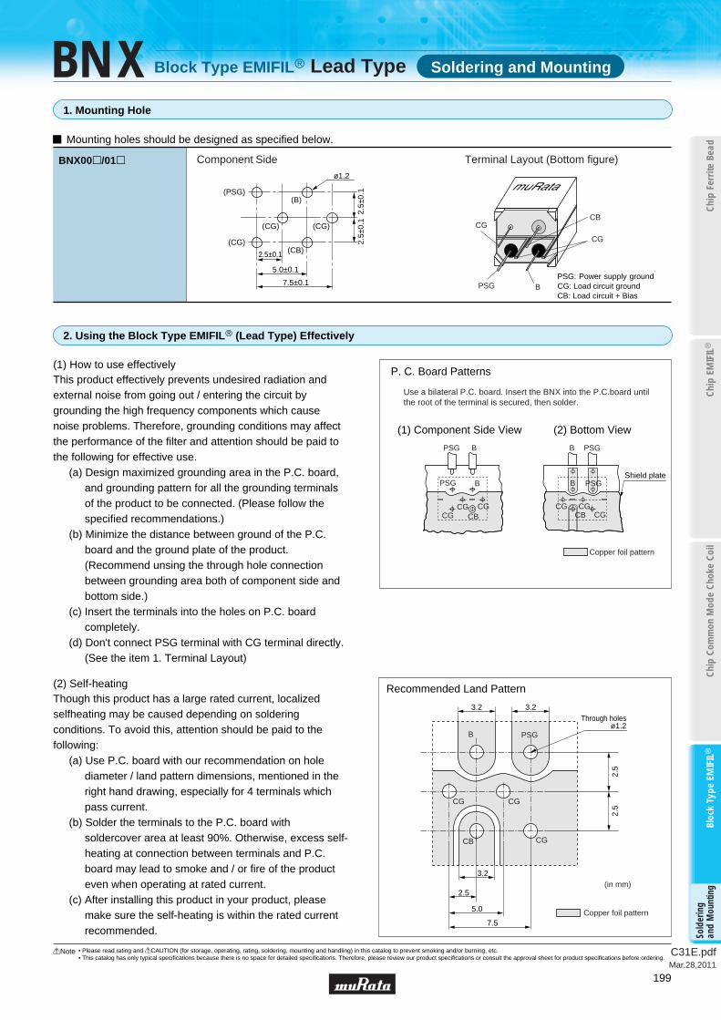
1. Mounting Hole
2. Using the Block Type EMIFILr (Lead Type) Effectively
Mounting holes should be designed as specified below.
BNX00p/01p Terminal Layout (Bottom figure)Component Side
7.5±0.1
(PSG)(B)
(CG)
(CG) (CG)
(CB)
5.0±0.1
2.5±0.1
2.5±
0.1
2.5±
0.1
ø1.2
PSG: Power supply groundCG: Load circuit groundCB: Load circuit + Bias
CG
CB CG
BPSG
This product effectively prevents undesired radiation and external noise from going out / entering the circuit by grounding the high frequency components which cause noise problems. Therefore, grounding conditions may affect the performance of the filter and attention should be paid to the following for effective use.
(a) Design maximized grounding area in the P.C. board, and grounding pattern for all the grounding terminals of the product to be connected. (Please follow the specified recommendations.)
(b) Minimize the distance between ground of the P.C. board and the ground plate of the product. (Recommend unsing the through hole connection between grounding area both of component side and bottom side.)
(c) Insert the terminals into the holes on P.C. board completely.
(d) Don't connect PSG terminal with CG terminal directly. (See the item 1. Terminal Layout)
(1) How to use effectively
Use a bilateral P.C. board. Insert the BNX into the P.C.board until the root of the terminal is secured, then solder.
PSGBB
CG CG CGCG
CGCG CB CB
PSG
PSG B
Copper foil pattern
PSGB
(1) Component Side View (2) Bottom View
Shield plate
P. C. Board Patterns
Though this product has a large rated current, localized selfheating may be caused depending on soldering conditions. To avoid this, attention should be paid to the following:
(a) Use P.C. board with our recommendation on hole diameter / land pattern dimensions, mentioned in the right hand drawing, especially for 4 terminals which pass current.
(b) Solder the terminals to the P.C. board with soldercover area at least 90%. Otherwise, excess self-heating at connection between terminals and P.C. board may lead to smoke and / or fire of the product even when operating at rated current.
(c) After installing this product in your product, please make sure the self-heating is within the rated current recommended.
(2) Self-heating
Copper foil pattern
(in mm)
Through holes
Recommended Land Pattern
PSGB
CG CG
CGCB
7.5
5.0
2.5
2.5
2.5
3.2
3.2 3.2
ø1.2
BNX Soldering and MountingBlock Type EMIFILr Lead Type

!Note • Please read rating and !CAUTION (for storage, operating, rating, soldering, mounting and handling) in this catalog to prevent smoking and/or burning, etc.• This catalog has only typical specifications because there is no space for detailed specifications. Therefore, please review our product specifications or consult the approval sheet for product specifications before ordering.
C31E.pdfMar.28,2011
Chip
Fer
rite
Bead
Chip
EM
IFILr
Chip
Com
mon
Mod
e Ch
oke
Coil
Bloc
k Ty
pe E
MIF
ILr
Sold
erin
g an
d M
ount
ing
200
3. Soldering
4. Cleaning
Clean the block Type EMIFILr(Lead Type) in the following conditions.(1) Cleaning temperature should be limited to 60°C max.
(40°C max for alcohol type cleaner).(2) Ultrasonic cleaning should comply with the following
conditions, avoiding the resonance phenomenon at the mounted products and P.C.B.Power: 20W/liter max. Frequency: 28 to 40kHz Time: 5 min. max.
(3) Cleaner(a) Alcohol type cleaner
Isopropyl alcohol (IPA)(b) Aqueous agent
Pine Alpha ST-100S
(4) There should be no residual flux or residual cleaner left after cleaning.In the case of using aqueous agent, products should be dried completely after rinsing with de-ionized water in order to remove the cleaner.
(5) The surface of products may become dirty after cleaning, but there is no deterioration on mechanical, electrical characteristics and reliability.
(6) Other cleaning: Please contact us.
(1) Use Sn-3.0Ag-0.5Cu solder.(2) Use Rosin-based flux. Do not use strong acidic flux with
halide content exceeding 0.2wt% (chlorine conversion value).
(3) Products and the leads should not be subjected to any mechanical stress during the soldering process, or while subjected to the equivalent high temperatures.
(4) Standard flow soldering profile
Solder Soldering Temperature Soldering Time
Sn-3.0Ag-0.5Cu solder 250 to 260˚C 4 to 6s
Pre-heating Soldering Gradual cooling(in air)
150°C
300
250
200
150
100
50
Tem
pera
ture
(°C
)
60s min. Soldering Time
Soldering temperature
Soldering and MountingBNX Block Type EMIFILr Lead Type

!Note • Please read rating and !CAUTION (for storage, operating, rating, soldering, mounting and handling) in this catalog to prevent smoking and/or burning, etc.• This catalog has only typical specifications because there is no space for detailed specifications. Therefore, please review our product specifications or consult the approval sheet for product specifications before ordering.
C31E.pdfMar.28,2011
Chip
Fer
rite
Bead
Chip
EM
IFILr
Chip
Com
mon
Mod
e Ch
oke
Coil
Bloc
k Ty
pe E
MIF
ILr
Pack
agin
g
201
BNX Block Type EMIFILr SMD Type
(in mm)
Minimum Quantity and Dimensions of 24mm Width Embossed Tape
BNX022/023
Part NumberCavity Size Minimum Qty. (pcs.)
12.4 9.4 3.3
cba
400 1500
ø180mm Reel ø330mm Reel
100
Bulk
4.0x10pitch=40.0±0.2
12.0±0.1
b: 9.4±0.1
3° max.
4.0±0.1 2.0±0.1
3.3±
0.1
11.5
±0.1
a: 1
2.4±
0.1
0.3±0.1
c: 3.3±0.1 c: Depth of Cavity
Dimension of the cavity is measured at the bottom side.
24.0
±0.2
1.75
±0.1
ø1.5 +0.1-0
ø1.5 +0.5-0
Packaging
"Minimum Quantity" means the number of units of each delivery or order. The quantity should be an integral multiple of the "Minimum Quantity".
BNX024/025
Part NumberCavity Size Minimum Qty. (pcs.)
12.4 9.4 3.6
cba
400 1500
ø180mm reel ø330mm reel
100
Bulk
4.0x10pitch=40.0±0.2
12.0±0.1
b: 9.4±0.1
4.0±0.1 2.0±0.1
3.6±
0.1
11.5
±0.1
a: 1
2.4±
0.1
0.3±0.1
c: 3.6±0.1
24.0
±0.2
1.75
±0.1
ø1.5 +0.1-0
ø1.5 +0.5-0
Dimension of the cavity is measured at the bottom side.

!Note • Please read rating and !CAUTION (for storage, operating, rating, soldering, mounting and handling) in this catalog to prevent smoking and/or burning, etc.• This catalog has only typical specifications because there is no space for detailed specifications. Therefore, please review our product specifications or consult the approval sheet for product specifications before ordering.
C31E.pdfMar.28,2011
Chip
Fer
rite
Bead
Chip
EM
IFILr
Chip
Com
mon
Mod
e Ch
oke
Coil
Bloc
k Ty
pe E
MIF
ILr
Des
ign
Kits
202
Part NumberNo.Rated Current
(A)Rated Voltage
(Vdc)Insertion Loss
Quantity(pcs.)
Part NumberNo.Rated Current
(A)Rated Voltage
(Vdc)Insertion Loss
Quantity(pcs.)
oEKEPBNX0A
oEKEPBLCKA
BNX002-01BNX012-01BNX016-01BNX012H01BNX022-01BNX023-01BNX024H01BNX025H01
12345678
11113333
1MHz to 1GHz : 40dB min.1MHz to 1GHz : 40dB min.
100kHz to 1GHz : 40dB min.1MHz to 1GHz : 40dB min.1MHz to 1GHz : 35dB min.1MHz to 1GHz : 35dB min.
100kHz to 1GHz : 35dB min.50kHz to 1GHz : 35dB min.
BNX002-01BNX003-01BNX005-01BNX012-01BNX016-01BNX012H01BNP002-02BNX022-01BNX023-01BNX024H01BNX025H01
1234567891011
11111113333
1MHz to 1GHz : 40dB min.5MHz to 1GHz : 40dB min.1MHz to 1GHz : 40dB min.1MHz to 1GHz : 40dB min.
100kHz to 1GHz : 40dB min.1MHz to 1GHz : 40dB min.
20MHz to 500MHz : 40dB min.1MHz to 1GHz : 35dB min.1MHz to 1GHz : 35dB min.
100kHz to 1GHz : 35dB min.50kHz to 1GHz : 35dB min.
5050255050
1005025
1015151510151515
50150505025505050
1005025
1010151515151010151515
Block Type EMIFILr BNX Design Kits