sn55110a, sn75110a, sn75112 (rev. g) - texas … − december 1975 − revised november 2004 4 post...
TRANSCRIPT
SLLS106G − DECEMBER 1975 − REVISED NOVEMBER 2004
1POST OFFICE BOX 655303 • DALLAS, TEXAS 75265
Improved Stability Over Supply Voltage andTemperature Ranges
Constant-Current Outputs
High Speed
Standard Supply Voltages
High Output Impedance
High Common-Mode Output Voltage Range. . . −3 V to 10 V
TTL-Input Compatibility
Inhibitor Available for Driver Selection
Glitch Free During Power Up/Power Down
SN75112 and External Circuit Meets orExceeds the Requirements of CCITTRecommendation V.35
description/ordering information
The SN55110A, SN75110A, and SN75112 dualline drivers have improved output currentregulation with supply-voltage and temperaturevariations. In addition, the higher current of theSN75112 (27 mA) allows data to be transmittedover longer lines. These drivers offer optimumperformance when used with the SN55107A,SN75107A, and SN75108A line receivers.
ORDERING INFORMATION
TA PACKAGE † ORDERABLEPART NUMBER
TOP-SIDEMARKING
PDIP (N) Tube of 25SN75110AN SN75110AN
PDIP (N) Tube of 25SN75112N SN75112N
Tube of 50 SN75110ADSN75110A
0°C to 70°CSOIC (D)
Reel of 2500 SN75110ADRSN75110A
0 C to 70 CSOIC (D)
Tube of 50 SN75112DSN75112
Reel of 2500 SN75112DRSN75112
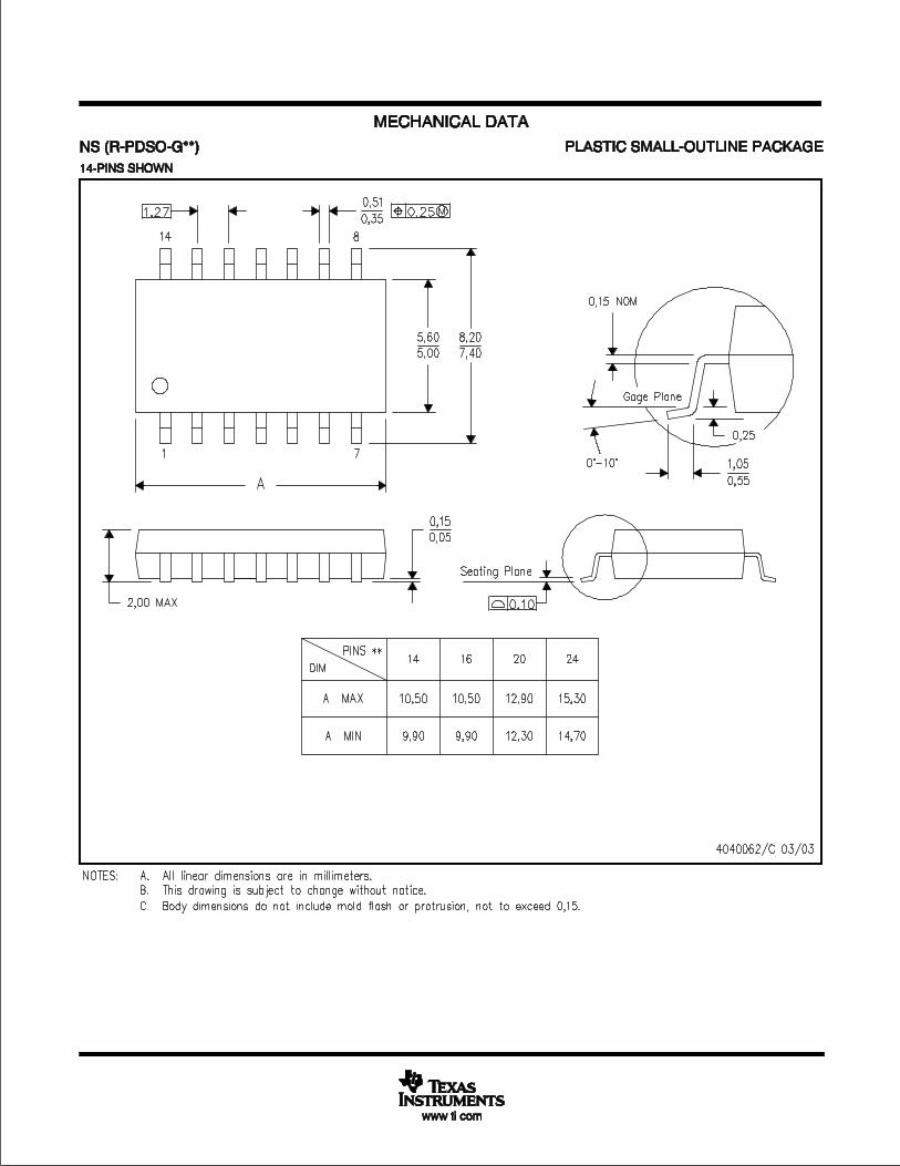
SOP (NS) Reel of 2000 SN75110ANSR SN75110A
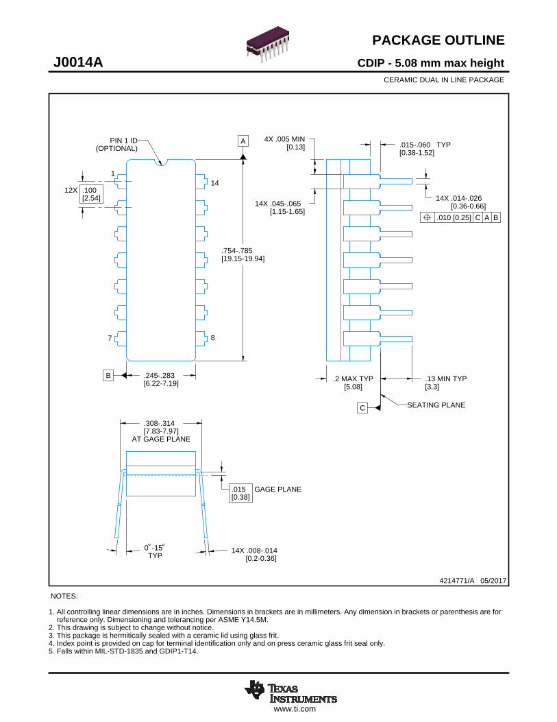
CDIP (J) Tube of 25SN55110AJ SN55110AJ
−55°C to 125°CCDIP (J) Tube of 25
SNJ55110AJ SNJ55110AJ−55°C to 125°C
CFP (W) Tube of 150 SNJ55110AW SNJ55110AW
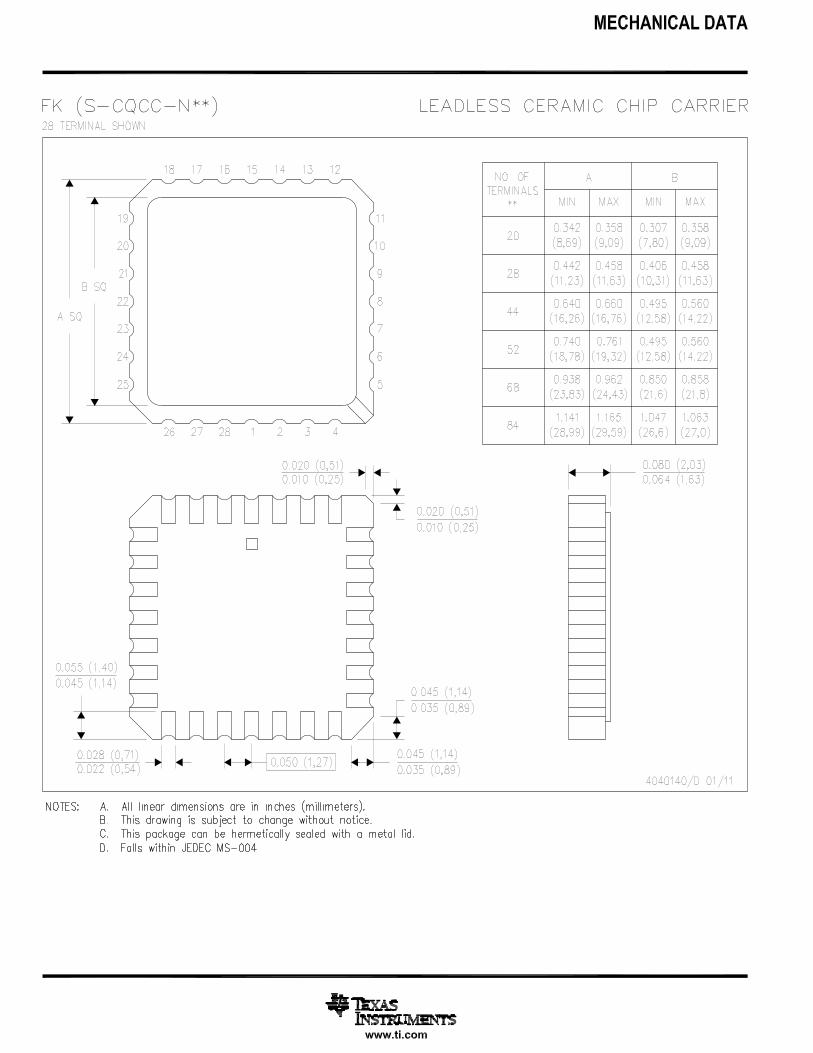
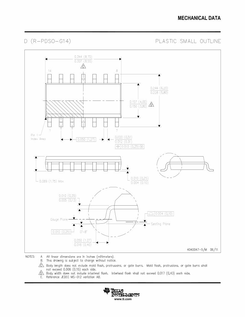
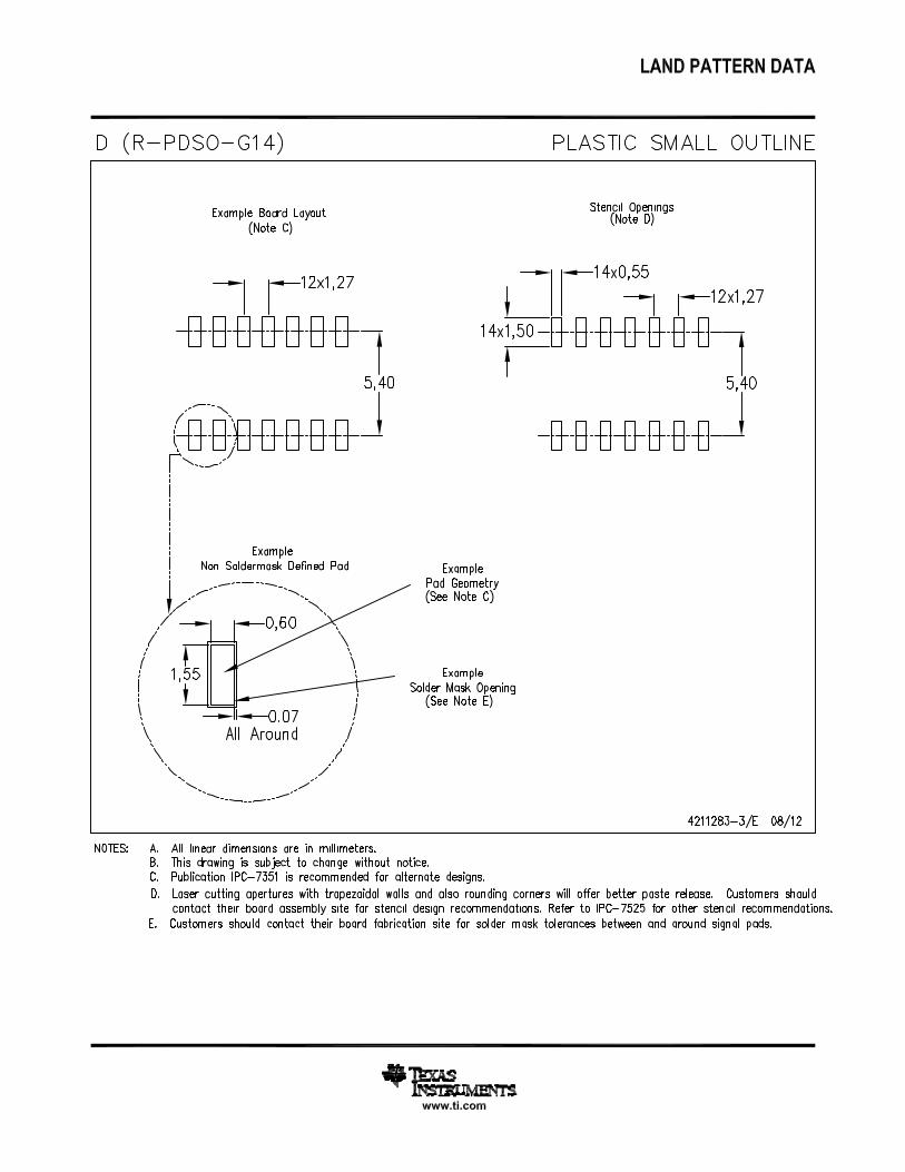
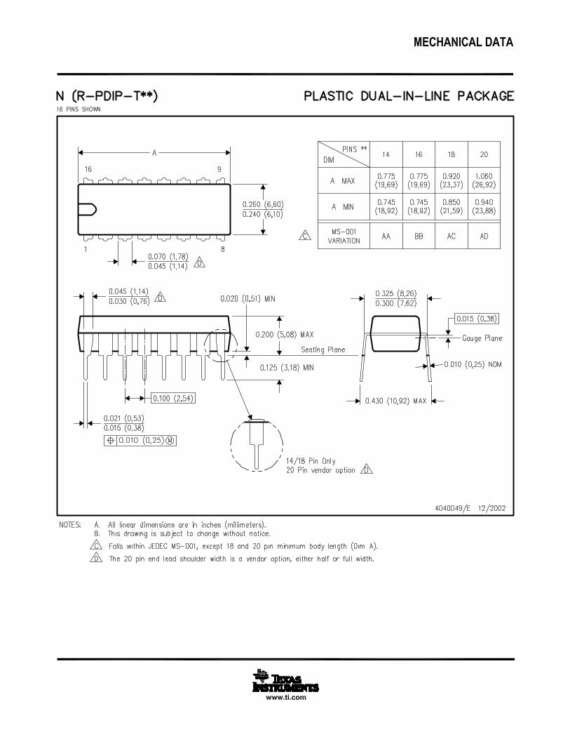
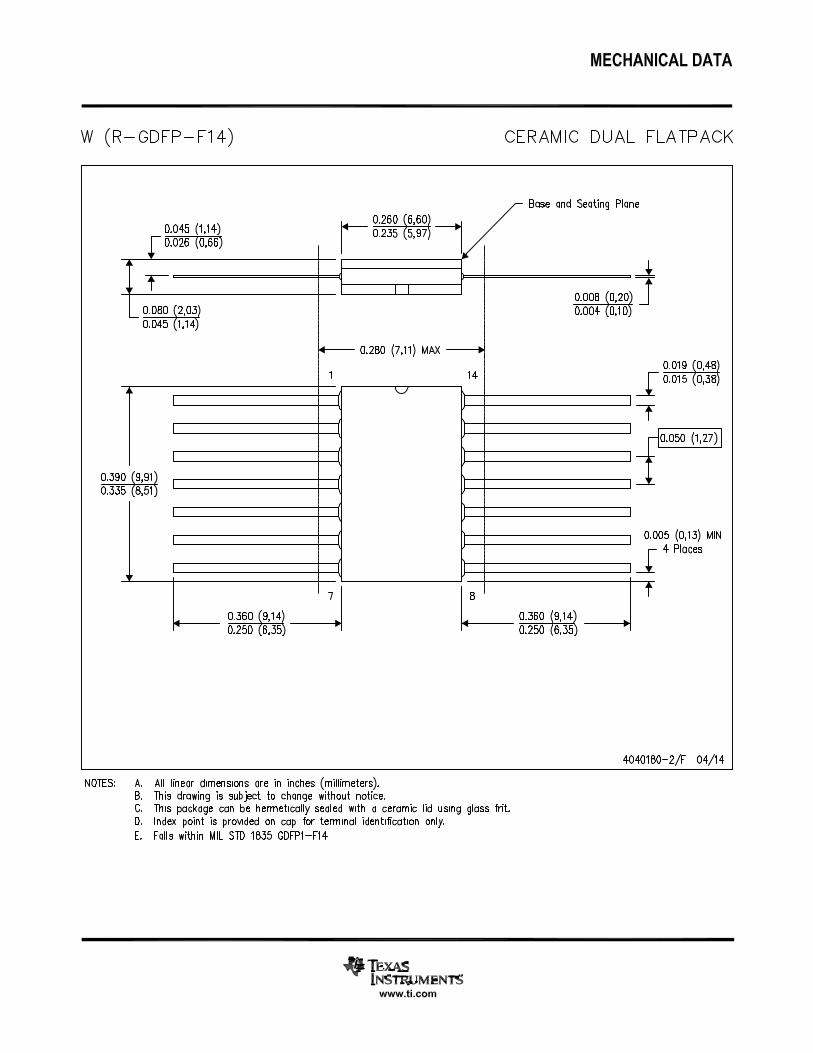
LCCC (FK) Tube of 55 SNJ55110AFK SNJ55110AFK† Package drawings, standard packing quantities, thermal data, symbolization, and PCB design guidelines
are available at www.ti.com/sc/package.
Please be aware that an important notice concerning availability, standard warranty, and use in critical applications ofTexas Instruments semiconductor products and disclaimers thereto appears at the end of this data sheet.
Copyright 2004, Texas Instruments Incorporated ! "#$ %!&% "! "! '! ! !( !%% )*& % "!+ %! !!$* $%!!+ $$ "!!&
1
2
3
4
5
6
7
14
13
12
11
10
9
8
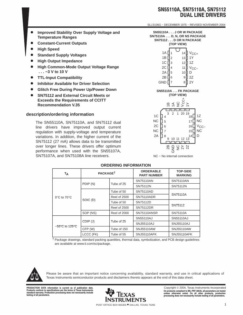
1A1B1C2C2A2B
GND
VCC+1Y1ZVCC−D2Z2Y
SN55110A . . . J OR W PACKAGESN75110A . . . D, N, OR NS PACKAGE
SN75112 . . . D OR N PACKAGE(TOP VIEW)
3 2 1 20 19
9 10 11 12 13
4
5
6
7
8
18
17
16
15
14
1ZNCVCC−NCD
1CNC2CNC2A
SN55110A . . . FK PACKAGE(TOP VIEW)
1B 1A NC
2Z1Y
2BG
ND
NC
CC
+V
2Y
NC − No internal connection
"% "$ , -.-/0/ $$ "!! ! !!%$! '!)! !%& $$ '! "% "%"!+ %! !!$* $%! !+ $$ "!!&
SLLS106G − DECEMBER 1975 − REVISED NOVEMBER 2004
2 POST OFFICE BOX 655303 • DALLAS, TEXAS 75265
description/ordering information (continued)
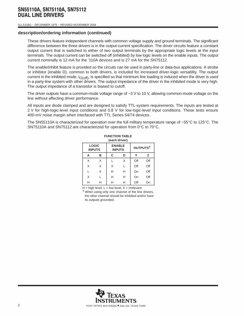
These drivers feature independent channels with common voltage supply and ground terminals. The significantdifference between the three drivers is in the output-current specification. The driver circuits feature a constantoutput current that is switched to either of two output terminals by the appropriate logic levels at the inputterminals. The output current can be switched off (inhibited) by low logic levels on the enable inputs. The outputcurrent nominally is 12 mA for the ’110A devices and is 27 mA for the SN75112.
The enable/inhibit feature is provided so the circuits can be used in party-line or data-bus applications. A strobeor inhibitor (enable D), common to both drivers, is included for increased driver-logic versatility. The outputcurrent in the inhibited mode, IO(off), is specified so that minimum line loading is induced when the driver is usedin a party-line system with other drivers. The output impedance of the driver in the inhibited mode is very high.The output impedance of a transistor is biased to cutoff.
The driver outputs have a common-mode voltage range of −3 V to 10 V, allowing common-mode voltage on theline without affecting driver performance.
All inputs are diode clamped and are designed to satisfy TTL-system requirements. The inputs are tested at2 V for high-logic-level input conditions and 0.8 V for low-logic-level input conditions. These tests ensure400-mV noise margin when interfaced with TTL Series 54/74 devices.
The SN55110A is characterized for operation over the full military temperature range of −55°C to 125°C. TheSN75110A and SN75112 are characterized for operation from 0°C to 70°C.
FUNCTION TABLE(each driver)
LOGICINPUTS
ENABLEINPUTS OUTPUTS†
A B C D Y Z
X X L X Off Off
X X X L Off Off
L X H H On Off
X L H H On Off
H H H H Off On
H = high level, L = low level, X = irrelevant† When using only one channel of the line drivers,
the other channel should be inhibited and/or haveits outputs grounded.

SLLS106G − DECEMBER 1975 − REVISED NOVEMBER 2004
3POST OFFICE BOX 655303 • DALLAS, TEXAS 75265
schematic (each driver)
To Other Driver
Y
Z
GND
B
A
. . . VCC+ Bus
. . . VCC− Bus
To OtherDriver
C
D
2.2 kΩNOM
VCC−
Common to Both Drivers
2.2 kΩNOM
VCC+
Pin numbers shown are for the D, J, N, NS, and W packages.
+
−
14
3, 4
10
1, 5
2, 6
7
11
8, 13
9, 12
+
−
−
−
+
+
− −
SLLS106G − DECEMBER 1975 − REVISED NOVEMBER 2004
4 POST OFFICE BOX 655303 • DALLAS, TEXAS 75265
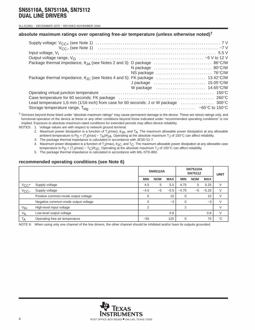
absolute maximum ratings over operating free-air temperature (unless otherwise noted) †
Supply voltage: VCC+ (see Note 1) 7 V. . . . . . . . . . . . . . . . . . . . . . . . . . . . . . . . . . . . . . . . . . . . . . . . . . . . . . . . . . . . VCC− (see Note 1) −7 V. . . . . . . . . . . . . . . . . . . . . . . . . . . . . . . . . . . . . . . . . . . . . . . . . . . . . . . . . .
Input voltage, VI 5.5 V. . . . . . . . . . . . . . . . . . . . . . . . . . . . . . . . . . . . . . . . . . . . . . . . . . . . . . . . . . . . . . . . . . . . . . . . . . Output voltage range, VO −5 V to 12 V. . . . . . . . . . . . . . . . . . . . . . . . . . . . . . . . . . . . . . . . . . . . . . . . . . . . . . . . . . . . Package thermal impedance, θJA (see Notes 2 and 3): D package 86°C/W. . . . . . . . . . . . . . . . . . . . . . . . . . . .
N package 80°C/W. . . . . . . . . . . . . . . . . . . . . . . . . . . . NS package 76°C/W. . . . . . . . . . . . . . . . . . . . . . . . . . .
Package thermal impedance, θJC (see Notes 4 and 5): FK package 13.42°C/W. . . . . . . . . . . . . . . . . . . . . . . . J package 15.05°C/W. . . . . . . . . . . . . . . . . . . . . . . . . W package 14.65°C/W. . . . . . . . . . . . . . . . . . . . . . . .
Operating virtual junction temperature 150°C. . . . . . . . . . . . . . . . . . . . . . . . . . . . . . . . . . . . . . . . . . . . . . . . . . . . . . Case temperature for 60 seconds: FK package 260°C. . . . . . . . . . . . . . . . . . . . . . . . . . . . . . . . . . . . . . . . . . . . . . Lead temperature 1,6 mm (1/16 inch) from case for 60 seconds: J or W package 300°C. . . . . . . . . . . . . . . . Storage temperature range, Tstg −65°C to 150°C. . . . . . . . . . . . . . . . . . . . . . . . . . . . . . . . . . . . . . . . . . . . . . . . . .
† Stresses beyond those listed under “absolute maximum ratings” may cause permanent damage to the device. These are stress ratings only, andfunctional operation of the device at these or any other conditions beyond those indicated under “recommended operating conditions” is notimplied. Exposure to absolute-maximum-rated conditions for extended periods may affect device reliability.
NOTES: 1. Voltage values are with respect to network ground terminal.2. Maximum power dissipation is a function of TJ(max), θJA, and TA. The maximum allowable power dissipation at any allowable
ambient temperature is PD = (TJ(max) − TA)/θJA. Operating at the absolute maximum TJ of 150°C can affect reliability.3. The package thermal impedance is calculated in accordance with JESD 51-7.4. Maximum power dissipation is a function of TJ(max), θJC, and TC. The maximum allowable power dissipation at any allowable case
temperature is PD = (TJ(max) − TC)/θJC. Operating at the absolute maximum TJ of 150°C can affect reliability.5. The package thermal impedance is calculated in accordance with MIL-STD-883.
recommended operating conditions (see Note 6)
SN55110ASN75110ASN75112 UNIT
MIN NOM MAX MIN NOM MAXUNIT
VCC+ Supply voltage 4.5 5 5.5 4.75 5 5.25 V
VCC− Supply voltage −4.5 −5 −5.5 −4.75 −5 −5.25 V
Positive common-mode output voltage 0 10 0 10 V
Negative common-mode output voltage 0 −3 0 −3 V
VIH High-level input voltage 2 2 V
VIL Low-level output voltage 0.8 0.8 V
TA Operating free-air temperature −55 125 0 70 °C
NOTE 6: When using only one channel of the line drivers, the other channel should be inhibited and/or have its outputs grounded.
SLLS106G − DECEMBER 1975 − REVISED NOVEMBER 2004
5POST OFFICE BOX 655303 • DALLAS, TEXAS 75265
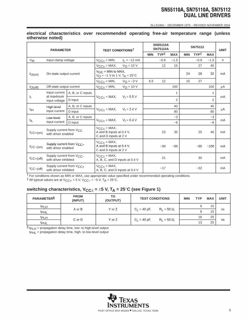
electrical characteristics over recommended operating free-air temperature range (unlessotherwise noted)
PARAMETER TEST CONDITIONS†SN55110ASN75110A SN75112
UNITPARAMETER TEST CONDITIONS†
MIN TYP‡ MAX MIN TYP‡ MAXUNIT
VIK Input clamp voltage VCC± = MIN, IL = −12 mA −0.9 −1.5 −0.9 −1.5 V
VCC± = MAX, VO = 10 V 12 15 27 40
IO(on) On-state output currentVCC = MIN to MAX,
24 28 32 mAIO(on) On-state output currentVCC = MIN to MAX,VO = −1 V to 1 V, TA = 25°C 24 28 32 mA
VCC± = MIN, VO = −3 V 6.5 12 15 27
IO(off) Off-state output current VCC± = MIN, VO = 10 V 100 100 µA
II
Input currentat maximum
A, B, or C inputsVCC = MAX, VI = 5.5 V
1 1mAII at maximum
input voltage D inputVCC± = MAX, VI = 5.5 V
2 2mA
IIHHigh-level A, B, or C inputs
VCC = MAX, VI = 2.4 V40 40
AIIHHigh-levelinput current D input
VCC± = MAX, VI = 2.4 V80 80
µA
IILLow-level A, B, or C inputs
VCC = MAX, VI = 0.4 V−3 −3
mAIILLow-levelinput current D input
VCC± = MAX, VI = 0.4 V−6 −6
mA
ICC+(on)Supply current from VCCwith driver enabled
VCC± = MAX,A and B inputs at 0.4 V,C and D inputs at 2 V
23 35 25 40 mA
ICC−(on)Supply current from VCC−
VCC± = MAX,A and B inputs at 0.4 V, −34 −50 −65 −100 mAICC−(on)
Supply current from VCC−with driver enabled
CCA and B inputs at 0.4 V,C and D inputs at 2 V
−34 −50 −65 −100 mA
ICC+(off)Supply current from VCC−with driver inhibited
VCC± = MAX,A, B, C, and D inputs at 0.4 V
21 30 mA
ICC−(off)Supply current from VCC±with driver inhibited
VCC± = MAX,A, B, C, and D inputs at 0.4 V
−17 −32 mA
† For conditions shown as MIN or MAX, use appropriate value specified under recommended operating conditions.‡ All typical values are at VCC+ = 5 V, VCC− = −5 V, TA = 25°C.
switching characteristics, V CC± = ±5 V, TA = 25°C (see Figure 1)
PARAMETER§ FROM(INPUT)
TO(OUTPUT) TEST CONDITIONS MIN TYP MAX UNIT
tPLHA or B Y or Z CL = 40 pF, RL = 50 Ω
9 15ns
tPHLA or B Y or Z CL = 40 pF, RL = 50 Ω,
9 15ns
tPLHC or D Y or Z CL = 40 pF, RL = 50 Ω
16 25ns
tPHLC or D Y or Z CL = 40 pF, RL = 50 Ω,
13 25ns
§ tPLH = propagation delay time, low- to high-level outputtPHL = propagation delay time, high- to low-level output
SLLS106G − DECEMBER 1975 − REVISED NOVEMBER 2004
6 POST OFFICE BOX 655303 • DALLAS, TEXAS 75265
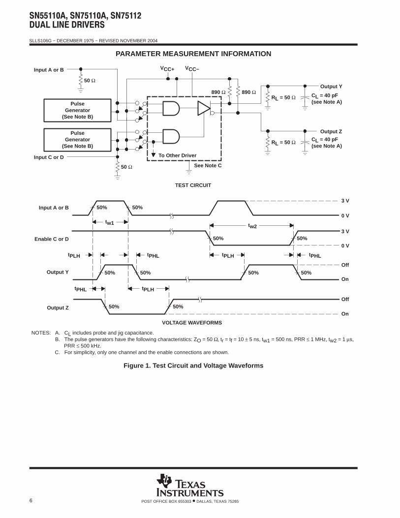
PARAMETER MEASUREMENT INFORMATION
Input A or B
PulseGenerator
(See Note B)
PulseGenerator
(See Note B)
Input A or B
Enable C or D
3 V
0 V
3 V
0 V
TEST CIRCUIT
Off
On
tPLH tPHL tPHLtPLH
tPHL
On
Off
Output Y
Output Z
VOLTAGE WAVEFORMS
890 ΩOutput Y
Output Z
RL = 50 Ω890 Ω
VCC+ VCC−
To Other Driver
50 Ω See Note C
RL = 50 Ω
50 Ω
Input C or D
CL = 40 pF(see Note A)
CL = 40 pF(see Note A)
NOTES: A. CL includes probe and jig capacitance.B. The pulse generators have the following characteristics: ZO = 50 Ω, tr = tf = 10 ± 5 ns, tw1 = 500 ns, PRR ≤ 1 MHz, tw2 = 1 µs,
PRR ≤ 500 kHz.C. For simplicity, only one channel and the enable connections are shown.
tw1 tw2
tPLH
50% 50%
50% 50%
50% 50% 50% 50%
50% 50%
Figure 1. Test Circuit and Voltage Waveforms
SLLS106G − DECEMBER 1975 − REVISED NOVEMBER 2004
7POST OFFICE BOX 655303 • DALLAS, TEXAS 75265
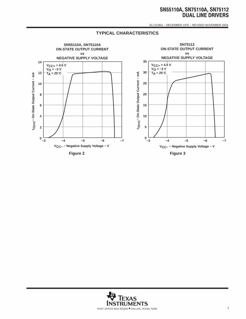
TYPICAL CHARACTERISTICS
VCC− − Negative Supply Voltage − V
Figure 2
12
10
8
6
4
14
−3 −7−4 −5 −6
2
0
− O
n-S
tate
Out
put C
urre
nt −
mA
I O(o
n)
SN55110A, SN75110AON-STATE OUTPUT CURRENT
vsNEGATIVE SUPPLY VOLTAGE
VCC+ = 4.5 VVO = −3 VTA = 25°C
Figure 3
−3
35
−70
−4 −5 −6
5
10
15
20
25
30
VCC− − Negative Supply Voltage − V
SN75112ON-STATE OUTPUT CURRENT
vsNEGATIVE SUPPLY VOLTAGE
VCC+ = 4.5 VVO = −3 VTA = 25°C
− O
n-S
tate
Out
put C
urre
nt −
mA
I O(o
n)
SLLS106G − DECEMBER 1975 − REVISED NOVEMBER 2004
8 POST OFFICE BOX 655303 • DALLAS, TEXAS 75265
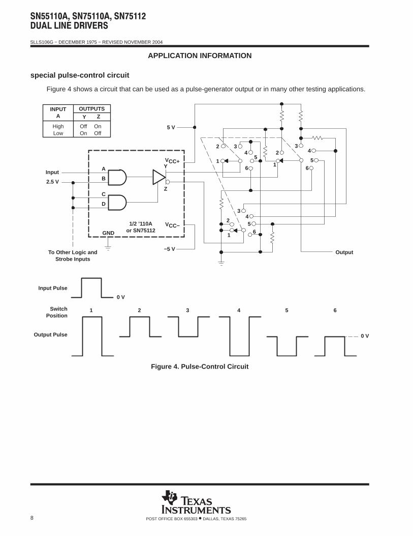
APPLICATION INFORMATION
special pulse-control circuit
Figure 4 shows a circuit that can be used as a pulse-generator output or in many other testing applications.
Input
2.5 V
To Other Logic andStrobe Inputs
1/2 ’110Aor SN75112
VCC−
VCC+
Output
Output Pulse
Input Pulse
SwitchPosition
0 V
0 V
INPUTA
HighLow
OffOn
OnOff
1 2 3 4 5 6
A
B
C
D
Y
Z
GND
−5 V
5 V
2
1
34
5
6
2
1
34
56
1
2
345
6
OUTPUTS
Y Z
Figure 4. Pulse-Control Circuit
SLLS106G − DECEMBER 1975 − REVISED NOVEMBER 2004
9POST OFFICE BOX 655303 • DALLAS, TEXAS 75265
APPLICATION INFORMATION
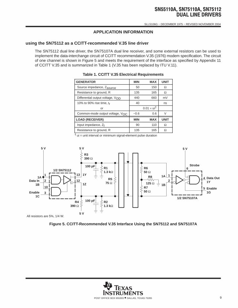
using the SN75112 as a CCITT-recommended V.35 line driver
The SN75112 dual line driver, the SN75107A dual line receiver, and some external resistors can be used toimplement the data-interchange circuit of CCITT recommendation V.35 (1976) modem specification. The circuitof one channel is shown in Figure 5 and meets the requirement of the interface as specified by Appendix 11of CCITT V.35 and is summarized in Table 1 (V.35 has been replaced by ITU V.11).
Table 1. CCITT V.35 Electrical Requirements
GENERATOR MIN MAX UNIT
Source impedance, Zsource 50 150 Ω
Resistance to ground, R 135 165 Ω
Differential output voltage, VOD 440 660 mV
10% to 90% rise time, tr 40 ns
or 0.01 × ui†
Common-mode output voltage, VOC −0.6 0.6 V
LOAD (RECEIVER) MIN MAX UNIT
Input impedance, ZI 90 110 Ω
Resistance to ground, R 135 165 Ω† ui = unit interval or minimum signal-element pulse duration
Data Out1YData In
1B
Enable1C
1A
R3390 Ω
R11.3 kΩ
R575 Ω
R4390 Ω
R21.3 kΩ
R650 Ω
R750 Ω
R8
100 pF
All resistors are 5%, 1/4 W.
5 V 5 V 5 V
5 V
13
12
1/2 SN75112
1
2
10
3
100 pF
1Y
1Z
1
2125 Ω
1A
1B
1/2 SN75107A
Enable1G
4
5
6Strobe
Figure 5. CCITT-Recommended V.35 Interface Using the SN75112 and SN75107A
PACKAGE OPTION ADDENDUM
www.ti.com 17-Mar-2017
Addendum-Page 1
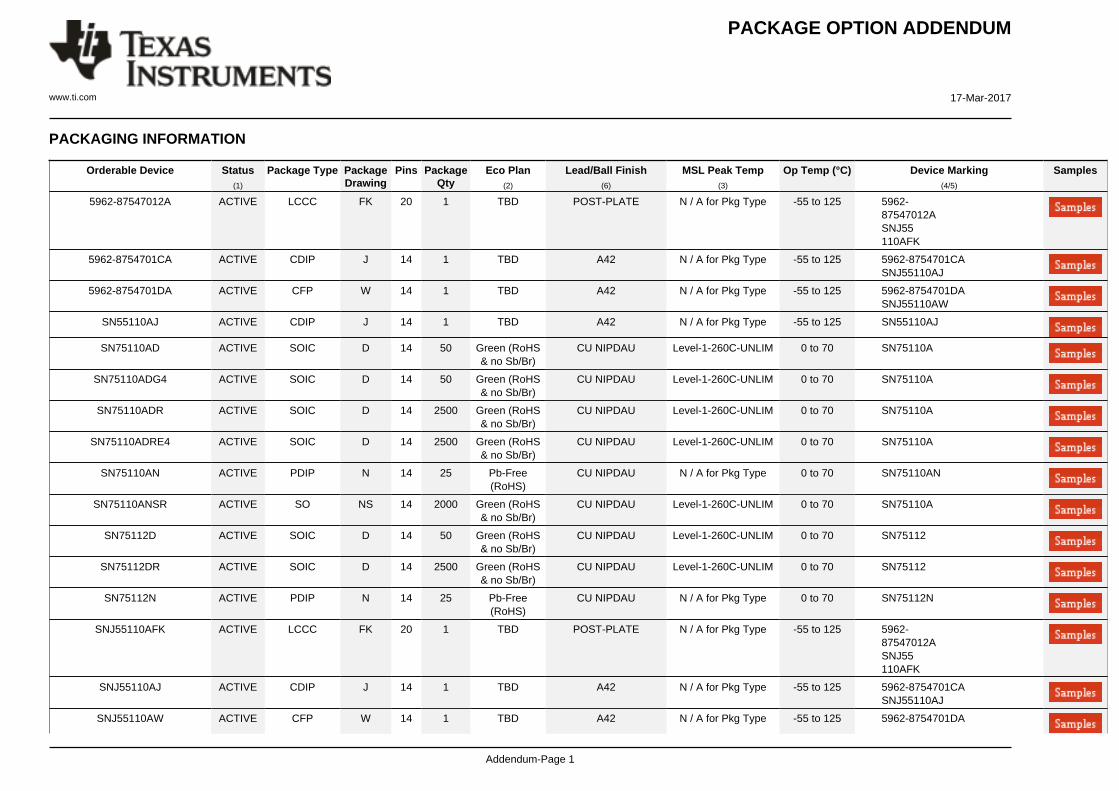
PACKAGING INFORMATION
Orderable Device Status(1)
Package Type PackageDrawing
Pins PackageQty
Eco Plan(2)
Lead/Ball Finish(6)
MSL Peak Temp(3)
Op Temp (°C) Device Marking(4/5)
Samples
5962-87547012A ACTIVE LCCC FK 20 1 TBD POST-PLATE N / A for Pkg Type -55 to 125 5962-87547012ASNJ55110AFK
5962-8754701CA ACTIVE CDIP J 14 1 TBD A42 N / A for Pkg Type -55 to 125 5962-8754701CASNJ55110AJ
5962-8754701DA ACTIVE CFP W 14 1 TBD A42 N / A for Pkg Type -55 to 125 5962-8754701DASNJ55110AW
SN55110AJ ACTIVE CDIP J 14 1 TBD A42 N / A for Pkg Type -55 to 125 SN55110AJ
SN75110AD ACTIVE SOIC D 14 50 Green (RoHS& no Sb/Br)
CU NIPDAU Level-1-260C-UNLIM 0 to 70 SN75110A
SN75110ADG4 ACTIVE SOIC D 14 50 Green (RoHS& no Sb/Br)
CU NIPDAU Level-1-260C-UNLIM 0 to 70 SN75110A
SN75110ADR ACTIVE SOIC D 14 2500 Green (RoHS& no Sb/Br)
CU NIPDAU Level-1-260C-UNLIM 0 to 70 SN75110A
SN75110ADRE4 ACTIVE SOIC D 14 2500 Green (RoHS& no Sb/Br)
CU NIPDAU Level-1-260C-UNLIM 0 to 70 SN75110A
SN75110AN ACTIVE PDIP N 14 25 Pb-Free(RoHS)
CU NIPDAU N / A for Pkg Type 0 to 70 SN75110AN
SN75110ANSR ACTIVE SO NS 14 2000 Green (RoHS& no Sb/Br)
CU NIPDAU Level-1-260C-UNLIM 0 to 70 SN75110A
SN75112D ACTIVE SOIC D 14 50 Green (RoHS& no Sb/Br)
CU NIPDAU Level-1-260C-UNLIM 0 to 70 SN75112
SN75112DR ACTIVE SOIC D 14 2500 Green (RoHS& no Sb/Br)
CU NIPDAU Level-1-260C-UNLIM 0 to 70 SN75112
SN75112N ACTIVE PDIP N 14 25 Pb-Free(RoHS)
CU NIPDAU N / A for Pkg Type 0 to 70 SN75112N
SNJ55110AFK ACTIVE LCCC FK 20 1 TBD POST-PLATE N / A for Pkg Type -55 to 125 5962-87547012ASNJ55110AFK
SNJ55110AJ ACTIVE CDIP J 14 1 TBD A42 N / A for Pkg Type -55 to 125 5962-8754701CASNJ55110AJ
SNJ55110AW ACTIVE CFP W 14 1 TBD A42 N / A for Pkg Type -55 to 125 5962-8754701DA
PACKAGE OPTION ADDENDUM
www.ti.com 17-Mar-2017
Addendum-Page 2
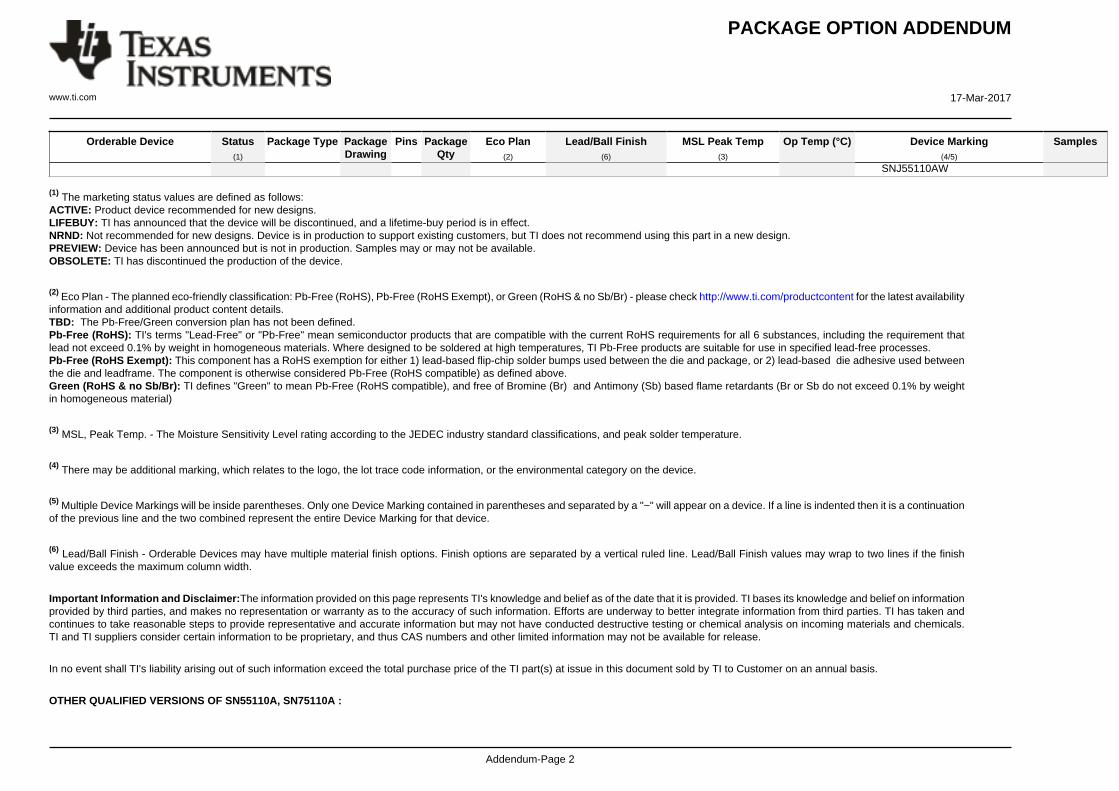
Orderable Device Status(1)
Package Type PackageDrawing
Pins PackageQty
Eco Plan(2)
Lead/Ball Finish(6)
MSL Peak Temp(3)
Op Temp (°C) Device Marking(4/5)
Samples
SNJ55110AW (1) The marketing status values are defined as follows:ACTIVE: Product device recommended for new designs.LIFEBUY: TI has announced that the device will be discontinued, and a lifetime-buy period is in effect.NRND: Not recommended for new designs. Device is in production to support existing customers, but TI does not recommend using this part in a new design.PREVIEW: Device has been announced but is not in production. Samples may or may not be available.OBSOLETE: TI has discontinued the production of the device.
(2) Eco Plan - The planned eco-friendly classification: Pb-Free (RoHS), Pb-Free (RoHS Exempt), or Green (RoHS & no Sb/Br) - please check http://www.ti.com/productcontent for the latest availabilityinformation and additional product content details.TBD: The Pb-Free/Green conversion plan has not been defined.Pb-Free (RoHS): TI's terms "Lead-Free" or "Pb-Free" mean semiconductor products that are compatible with the current RoHS requirements for all 6 substances, including the requirement thatlead not exceed 0.1% by weight in homogeneous materials. Where designed to be soldered at high temperatures, TI Pb-Free products are suitable for use in specified lead-free processes.Pb-Free (RoHS Exempt): This component has a RoHS exemption for either 1) lead-based flip-chip solder bumps used between the die and package, or 2) lead-based die adhesive used betweenthe die and leadframe. The component is otherwise considered Pb-Free (RoHS compatible) as defined above.Green (RoHS & no Sb/Br): TI defines "Green" to mean Pb-Free (RoHS compatible), and free of Bromine (Br) and Antimony (Sb) based flame retardants (Br or Sb do not exceed 0.1% by weightin homogeneous material)
(3) MSL, Peak Temp. - The Moisture Sensitivity Level rating according to the JEDEC industry standard classifications, and peak solder temperature.
(4) There may be additional marking, which relates to the logo, the lot trace code information, or the environmental category on the device.
(5) Multiple Device Markings will be inside parentheses. Only one Device Marking contained in parentheses and separated by a "~" will appear on a device. If a line is indented then it is a continuationof the previous line and the two combined represent the entire Device Marking for that device.
(6) Lead/Ball Finish - Orderable Devices may have multiple material finish options. Finish options are separated by a vertical ruled line. Lead/Ball Finish values may wrap to two lines if the finishvalue exceeds the maximum column width.
Important Information and Disclaimer:The information provided on this page represents TI's knowledge and belief as of the date that it is provided. TI bases its knowledge and belief on informationprovided by third parties, and makes no representation or warranty as to the accuracy of such information. Efforts are underway to better integrate information from third parties. TI has taken andcontinues to take reasonable steps to provide representative and accurate information but may not have conducted destructive testing or chemical analysis on incoming materials and chemicals.TI and TI suppliers consider certain information to be proprietary, and thus CAS numbers and other limited information may not be available for release.
In no event shall TI's liability arising out of such information exceed the total purchase price of the TI part(s) at issue in this document sold by TI to Customer on an annual basis.
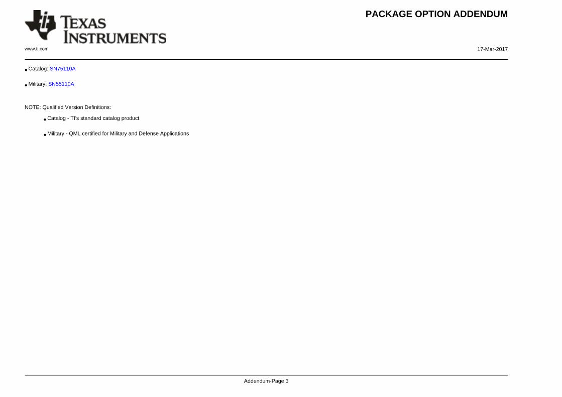
OTHER QUALIFIED VERSIONS OF SN55110A, SN75110A :
PACKAGE OPTION ADDENDUM
www.ti.com 17-Mar-2017
Addendum-Page 3
• Catalog: SN75110A
• Military: SN55110A
NOTE: Qualified Version Definitions:
• Catalog - TI's standard catalog product
• Military - QML certified for Military and Defense Applications
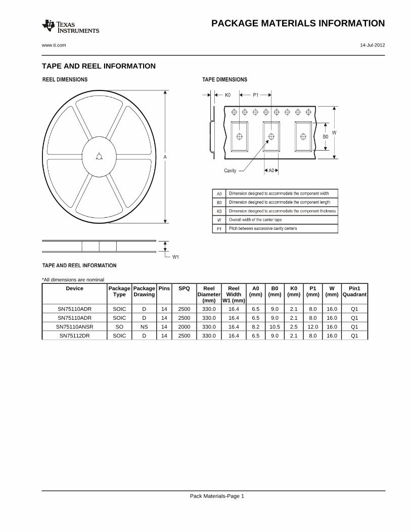
TAPE AND REEL INFORMATION
*All dimensions are nominal
Device PackageType
PackageDrawing
Pins SPQ ReelDiameter
(mm)
ReelWidth
W1 (mm)
A0(mm)
B0(mm)
K0(mm)
P1(mm)
W(mm)
Pin1Quadrant
SN75110ADR SOIC D 14 2500 330.0 16.4 6.5 9.0 2.1 8.0 16.0 Q1
SN75110ADR SOIC D 14 2500 330.0 16.4 6.5 9.0 2.1 8.0 16.0 Q1
SN75110ANSR SO NS 14 2000 330.0 16.4 8.2 10.5 2.5 12.0 16.0 Q1
SN75112DR SOIC D 14 2500 330.0 16.4 6.5 9.0 2.1 8.0 16.0 Q1
PACKAGE MATERIALS INFORMATION
www.ti.com 14-Jul-2012
Pack Materials-Page 1

*All dimensions are nominal
Device Package Type Package Drawing Pins SPQ Length (mm) Width (mm) Height (mm)
SN75110ADR SOIC D 14 2500 333.2 345.9 28.6
SN75110ADR SOIC D 14 2500 367.0 367.0 38.0
SN75110ANSR SO NS 14 2000 367.0 367.0 38.0
SN75112DR SOIC D 14 2500 367.0 367.0 38.0
PACKAGE MATERIALS INFORMATION
www.ti.com 14-Jul-2012
Pack Materials-Page 2

www.ti.com
PACKAGE OUTLINE
C
14X .008-.014 [0.2-0.36]TYP
-150
AT GAGE PLANE
-.314.308-7.977.83[ ]
14X -.026.014-0.660.36[ ]14X -.065.045
-1.651.15[ ]
.2 MAX TYP[5.08]
.13 MIN TYP[3.3]
TYP-.060.015-1.520.38[ ]
4X .005 MIN[0.13]
12X .100[2.54]
.015 GAGE PLANE[0.38]
A
-.785.754-19.9419.15[ ]
B -.283.245-7.196.22[ ]
CDIP - 5.08 mm max heightJ0014ACERAMIC DUAL IN LINE PACKAGE
4214771/A 05/2017
NOTES: 1. All controlling linear dimensions are in inches. Dimensions in brackets are in millimeters. Any dimension in brackets or parenthesis are for reference only. Dimensioning and tolerancing per ASME Y14.5M.2. This drawing is subject to change without notice. 3. This package is hermitically sealed with a ceramic lid using glass frit.4. Index point is provided on cap for terminal identification only and on press ceramic glass frit seal only.5. Falls within MIL-STD-1835 and GDIP1-T14.
7 8
141
PIN 1 ID(OPTIONAL)
SCALE 0.900
SEATING PLANE
.010 [0.25] C A B
www.ti.com
EXAMPLE BOARD LAYOUT
ALL AROUND[0.05]
MAX.002
.002 MAX[0.05]ALL AROUND
SOLDER MASKOPENING
METAL
(.063)[1.6]
(R.002 ) TYP[0.05]
14X ( .039)[1]
( .063)[1.6]
12X (.100 )[2.54]
(.300 ) TYP[7.62]
CDIP - 5.08 mm max heightJ0014ACERAMIC DUAL IN LINE PACKAGE
4214771/A 05/2017
LAND PATTERN EXAMPLENON-SOLDER MASK DEFINED
SCALE: 5X
SEE DETAIL A SEE DETAIL B
SYMM
SYMM
1
7 8
14
DETAIL ASCALE: 15X
SOLDER MASKOPENING
METAL
DETAIL B13X, SCALE: 15X

IMPORTANT NOTICE
Texas Instruments Incorporated (TI) reserves the right to make corrections, enhancements, improvements and other changes to itssemiconductor products and services per JESD46, latest issue, and to discontinue any product or service per JESD48, latest issue. Buyersshould obtain the latest relevant information before placing orders and should verify that such information is current and complete.TI’s published terms of sale for semiconductor products (http://www.ti.com/sc/docs/stdterms.htm) apply to the sale of packaged integratedcircuit products that TI has qualified and released to market. Additional terms may apply to the use or sale of other types of TI products andservices.Reproduction of significant portions of TI information in TI data sheets is permissible only if reproduction is without alteration and isaccompanied by all associated warranties, conditions, limitations, and notices. TI is not responsible or liable for such reproduceddocumentation. Information of third parties may be subject to additional restrictions. Resale of TI products or services with statementsdifferent from or beyond the parameters stated by TI for that product or service voids all express and any implied warranties for theassociated TI product or service and is an unfair and deceptive business practice. TI is not responsible or liable for any such statements.Buyers and others who are developing systems that incorporate TI products (collectively, “Designers”) understand and agree that Designersremain responsible for using their independent analysis, evaluation and judgment in designing their applications and that Designers havefull and exclusive responsibility to assure the safety of Designers' applications and compliance of their applications (and of all TI productsused in or for Designers’ applications) with all applicable regulations, laws and other applicable requirements. Designer represents that, withrespect to their applications, Designer has all the necessary expertise to create and implement safeguards that (1) anticipate dangerousconsequences of failures, (2) monitor failures and their consequences, and (3) lessen the likelihood of failures that might cause harm andtake appropriate actions. Designer agrees that prior to using or distributing any applications that include TI products, Designer willthoroughly test such applications and the functionality of such TI products as used in such applications.TI’s provision of technical, application or other design advice, quality characterization, reliability data or other services or information,including, but not limited to, reference designs and materials relating to evaluation modules, (collectively, “TI Resources”) are intended toassist designers who are developing applications that incorporate TI products; by downloading, accessing or using TI Resources in anyway, Designer (individually or, if Designer is acting on behalf of a company, Designer’s company) agrees to use any particular TI Resourcesolely for this purpose and subject to the terms of this Notice.TI’s provision of TI Resources does not expand or otherwise alter TI’s applicable published warranties or warranty disclaimers for TIproducts, and no additional obligations or liabilities arise from TI providing such TI Resources. TI reserves the right to make corrections,enhancements, improvements and other changes to its TI Resources. TI has not conducted any testing other than that specificallydescribed in the published documentation for a particular TI Resource.Designer is authorized to use, copy and modify any individual TI Resource only in connection with the development of applications thatinclude the TI product(s) identified in such TI Resource. NO OTHER LICENSE, EXPRESS OR IMPLIED, BY ESTOPPEL OR OTHERWISETO ANY OTHER TI INTELLECTUAL PROPERTY RIGHT, AND NO LICENSE TO ANY TECHNOLOGY OR INTELLECTUAL PROPERTYRIGHT OF TI OR ANY THIRD PARTY IS GRANTED HEREIN, including but not limited to any patent right, copyright, mask work right, orother intellectual property right relating to any combination, machine, or process in which TI products or services are used. Informationregarding or referencing third-party products or services does not constitute a license to use such products or services, or a warranty orendorsement thereof. Use of TI Resources may require a license from a third party under the patents or other intellectual property of thethird party, or a license from TI under the patents or other intellectual property of TI.TI RESOURCES ARE PROVIDED “AS IS” AND WITH ALL FAULTS. TI DISCLAIMS ALL OTHER WARRANTIES ORREPRESENTATIONS, EXPRESS OR IMPLIED, REGARDING RESOURCES OR USE THEREOF, INCLUDING BUT NOT LIMITED TOACCURACY OR COMPLETENESS, TITLE, ANY EPIDEMIC FAILURE WARRANTY AND ANY IMPLIED WARRANTIES OFMERCHANTABILITY, FITNESS FOR A PARTICULAR PURPOSE, AND NON-INFRINGEMENT OF ANY THIRD PARTY INTELLECTUALPROPERTY RIGHTS. TI SHALL NOT BE LIABLE FOR AND SHALL NOT DEFEND OR INDEMNIFY DESIGNER AGAINST ANY CLAIM,INCLUDING BUT NOT LIMITED TO ANY INFRINGEMENT CLAIM THAT RELATES TO OR IS BASED ON ANY COMBINATION OFPRODUCTS EVEN IF DESCRIBED IN TI RESOURCES OR OTHERWISE. IN NO EVENT SHALL TI BE LIABLE FOR ANY ACTUAL,DIRECT, SPECIAL, COLLATERAL, INDIRECT, PUNITIVE, INCIDENTAL, CONSEQUENTIAL OR EXEMPLARY DAMAGES INCONNECTION WITH OR ARISING OUT OF TI RESOURCES OR USE THEREOF, AND REGARDLESS OF WHETHER TI HAS BEENADVISED OF THE POSSIBILITY OF SUCH DAMAGES.Unless TI has explicitly designated an individual product as meeting the requirements of a particular industry standard (e.g., ISO/TS 16949and ISO 26262), TI is not responsible for any failure to meet such industry standard requirements.Where TI specifically promotes products as facilitating functional safety or as compliant with industry functional safety standards, suchproducts are intended to help enable customers to design and create their own applications that meet applicable functional safety standardsand requirements. Using products in an application does not by itself establish any safety features in the application. Designers mustensure compliance with safety-related requirements and standards applicable to their applications. Designer may not use any TI products inlife-critical medical equipment unless authorized officers of the parties have executed a special contract specifically governing such use.Life-critical medical equipment is medical equipment where failure of such equipment would cause serious bodily injury or death (e.g., lifesupport, pacemakers, defibrillators, heart pumps, neurostimulators, and implantables). Such equipment includes, without limitation, allmedical devices identified by the U.S. Food and Drug Administration as Class III devices and equivalent classifications outside the U.S.TI may expressly designate certain products as completing a particular qualification (e.g., Q100, Military Grade, or Enhanced Product).Designers agree that it has the necessary expertise to select the product with the appropriate qualification designation for their applicationsand that proper product selection is at Designers’ own risk. Designers are solely responsible for compliance with all legal and regulatoryrequirements in connection with such selection.Designer will fully indemnify TI and its representatives against any damages, costs, losses, and/or liabilities arising out of Designer’s non-compliance with the terms and provisions of this Notice.
Mailing Address: Texas Instruments, Post Office Box 655303, Dallas, Texas 75265Copyright © 2017, Texas Instruments Incorporated