sn74lvc1g07 single buffer/driver with open-drain … single buffer/driver with open-drain output ......
TRANSCRIPT
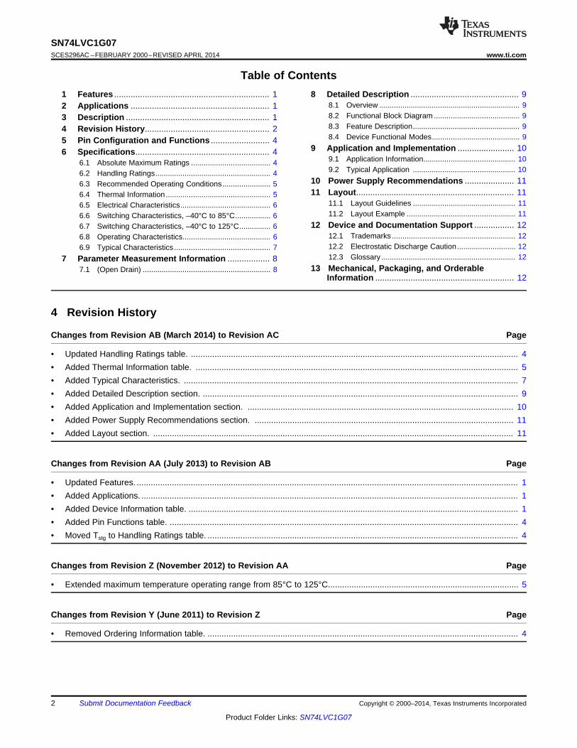
A Y
Product
Folder
Sample &Buy
Technical
Documents
Tools &
Software
Support &Community
SN74LVC1G07SCES296AC –FEBRUARY 2000–REVISED APRIL 2014
SN74LVC1G07 Single Buffer/Driver With Open-Drain Output1 Features 3 Description
This single buffer/driver is designed for 1.65-V to1• Available in the Ultra Small 0.64-mm2
5.5-V VCC operation.Package (DPW) With 0.5-mm PitchThe output of the SN74LVC1G07 device is open• Supports 5-V VCC Operationdrain and can be connected to other open-drain• Input and Open-Drain Output Accept outputs to implement active-low wired-OR or active-Voltages up to 5.5 V high wired-AND functions. The maximum sink current
• Can Translate Up or Down is 32 mA.• Max tpd of 4.2 ns at 3.3 V The SN74LVC1G07 is available in a variety of• Low Power Consumption, 10-µA Max ICC packages, including the ultra-small DPW package
with a body size of 0.8 mm × 0.8 mm.• ±24-mA Output Drive at 3.3 V• Ioff Supports Live Insertion, Partial-Power-Down white space
Mode, and Back-Drive Protection white space• Latch-Up Performance Exceeds 100 mA Per
JESD 78, Class II Device Information(1)
• ESD Protection Exceeds JESD 22 DEVICE NAME PACKAGE BODY SIZESOT-23 (5) 2.9mm × 1.6mm– 2000-V Human-Body Model (A114-A)SC70 (5) 2.0mm × 1.25mm– 200-V Machine Model (A115-A)
SN74LVC1G07 X2SON (4) 0.8mm × 0.8mm– 1000-V Charged-Device Model (C101)SON (6) 1.45mm × 1.0mmSON (6) 1.0mm × 1.0mm2 Applications
(1) For all available packages, see the orderable addendum at• AV Receiverthe end of the datasheet.• Blu-ray Player and Home Theater
• DVD Recorder and Player• Desktop or Notebook PC• Digital Radio or Internet Radio Player• Digital Video Camera (DVC)• Embedded PC• GPS: Personal Navigation Device• Mobile Internet Device• Network Projector Front End• Portable Media Player• Pro Audio Mixer• Smoke Detector• Solid State Drive (SSD): Enterprise• High-Definition (HDTV)• Tablet: Enterprise• Audio Dock: Portable• DLP Front Projection System• DVR and DVS• Digital Picture Frame (DPF)• Digital Still Camera
1
An IMPORTANT NOTICE at the end of this data sheet addresses availability, warranty, changes, use in safety-critical applications,intellectual property matters and other important disclaimers. PRODUCTION DATA.
SN74LVC1G07SCES296AC –FEBRUARY 2000–REVISED APRIL 2014 www.ti.com
Table of Contents1 Features .................................................................. 1 8 Detailed Description .............................................. 9
8.1 Overview ................................................................... 92 Applications ........................................................... 18.2 Functional Block Diagram ......................................... 93 Description ............................................................. 18.3 Feature Description................................................... 94 Revision History..................................................... 28.4 Device Functional Modes.......................................... 95 Pin Configuration and Functions ......................... 4
9 Application and Implementation ........................ 106 Specifications......................................................... 49.1 Application Information............................................ 106.1 Absolute Maximum Ratings ...................................... 49.2 Typical Application ................................................. 106.2 Handling Ratings....................................................... 4
10 Power Supply Recommendations ..................... 116.3 Recommended Operating Conditions....................... 511 Layout................................................................... 116.4 Thermal Information .................................................. 5
11.1 Layout Guidelines ................................................. 116.5 Electrical Characteristics........................................... 611.2 Layout Example .................................................... 116.6 Switching Characteristics, –40°C to 85°C................. 6
12 Device and Documentation Support ................. 126.7 Switching Characteristics, –40°C to 125°C............... 612.1 Trademarks ........................................................... 126.8 Operating Characteristics.......................................... 612.2 Electrostatic Discharge Caution............................ 126.9 Typical Characteristics .............................................. 712.3 Glossary ................................................................ 127 Parameter Measurement Information .................. 8
13 Mechanical, Packaging, and Orderable7.1 (Open Drain) ............................................................. 8Information ........................................................... 12
4 Revision History
Changes from Revision AB (March 2014) to Revision AC Page
• Updated Handling Ratings table. ........................................................................................................................................... 4• Added Thermal Information table. ......................................................................................................................................... 5• Added Typical Characteristics. .............................................................................................................................................. 7• Added Detailed Description section. ...................................................................................................................................... 9• Added Application and Implementation section. ................................................................................................................. 10• Added Power Supply Recommendations section. .............................................................................................................. 11• Added Layout section. ......................................................................................................................................................... 11
Changes from Revision AA (July 2013) to Revision AB Page
• Updated Features. .................................................................................................................................................................. 1• Added Applications. ................................................................................................................................................................ 1• Added Device Information table. ............................................................................................................................................ 1• Added Pin Functions table. .................................................................................................................................................... 4• Moved Tstg to Handling Ratings table. .................................................................................................................................... 4
Changes from Revision Z (November 2012) to Revision AA Page
• Extended maximum temperature operating range from 85°C to 125°C................................................................................. 5
Changes from Revision Y (June 2011) to Revision Z Page
• Removed Ordering Information table. .................................................................................................................................... 4
2 Submit Documentation Feedback Copyright © 2000–2014, Texas Instruments Incorporated
Product Folder Links: SN74LVC1G07
SN74LVC1G07www.ti.com SCES296AC –FEBRUARY 2000–REVISED APRIL 2014
Changes from Revision W (June 2008) to Revision X Page
• Added DSF Package to data sheet. ....................................................................................................................................... 4
Copyright © 2000–2014, Texas Instruments Incorporated Submit Documentation Feedback 3
Product Folder Links: SN74LVC1G07
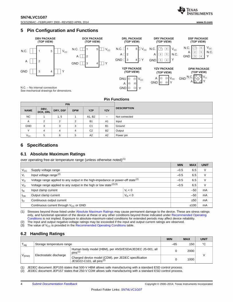
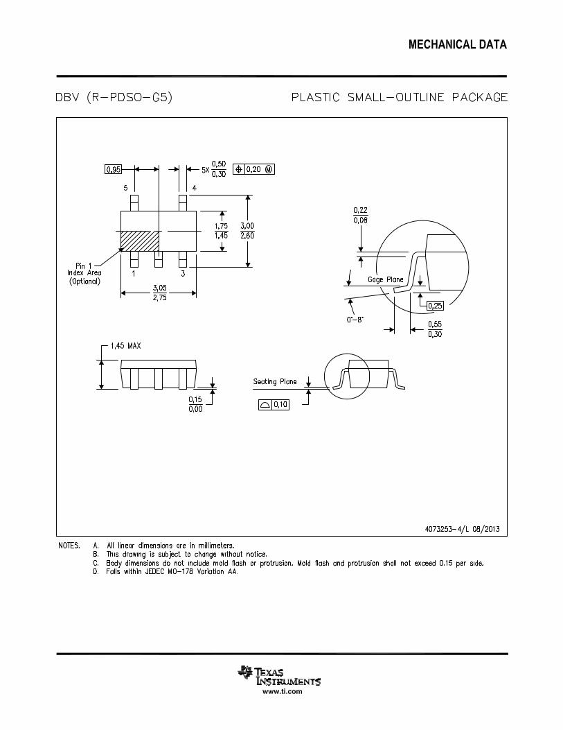
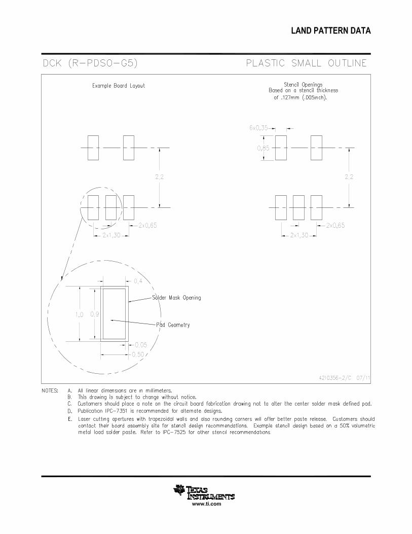
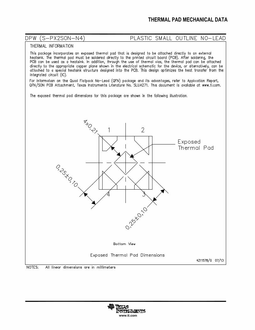
N.C. – No internal connectionSee mechanical drawings for dimensions.
DBV PACKAGE(TOP VIEW)
2
5
3 4 Y
1
A
GND
N.C. VCC
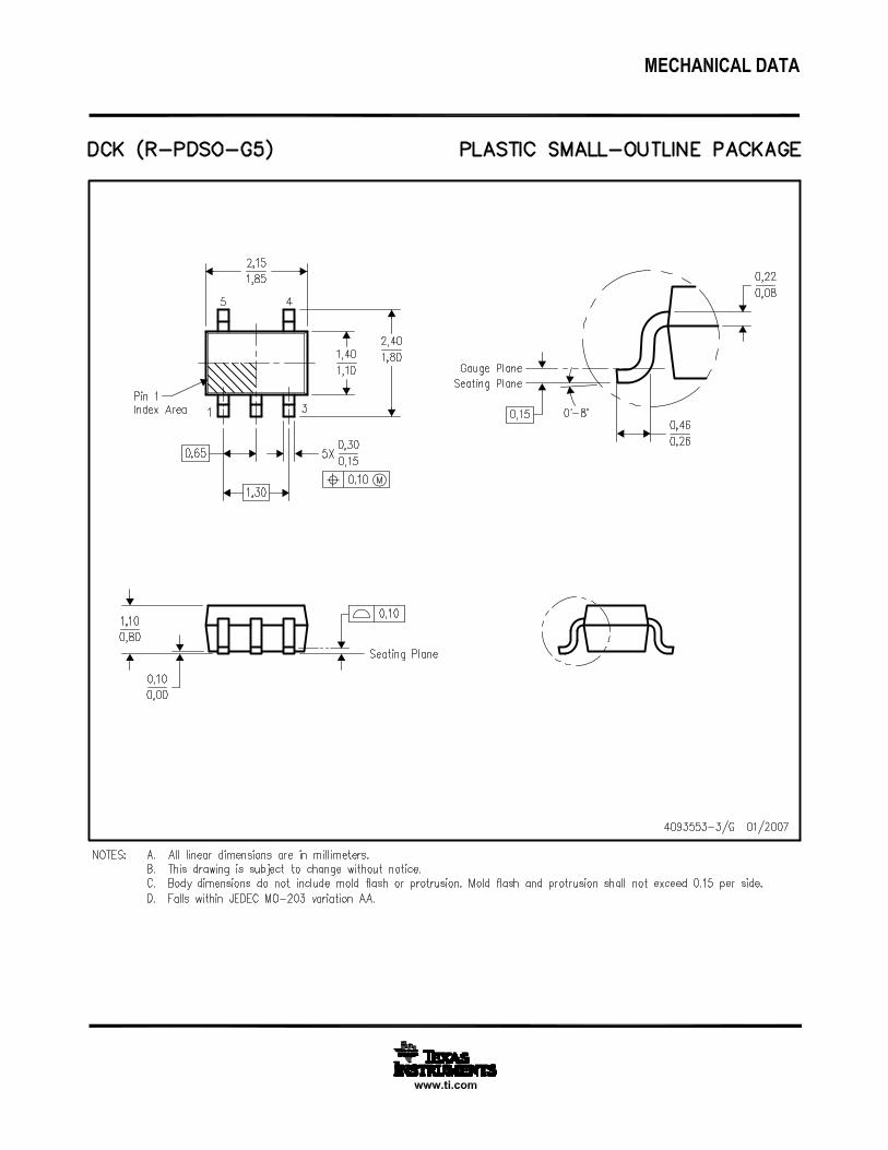
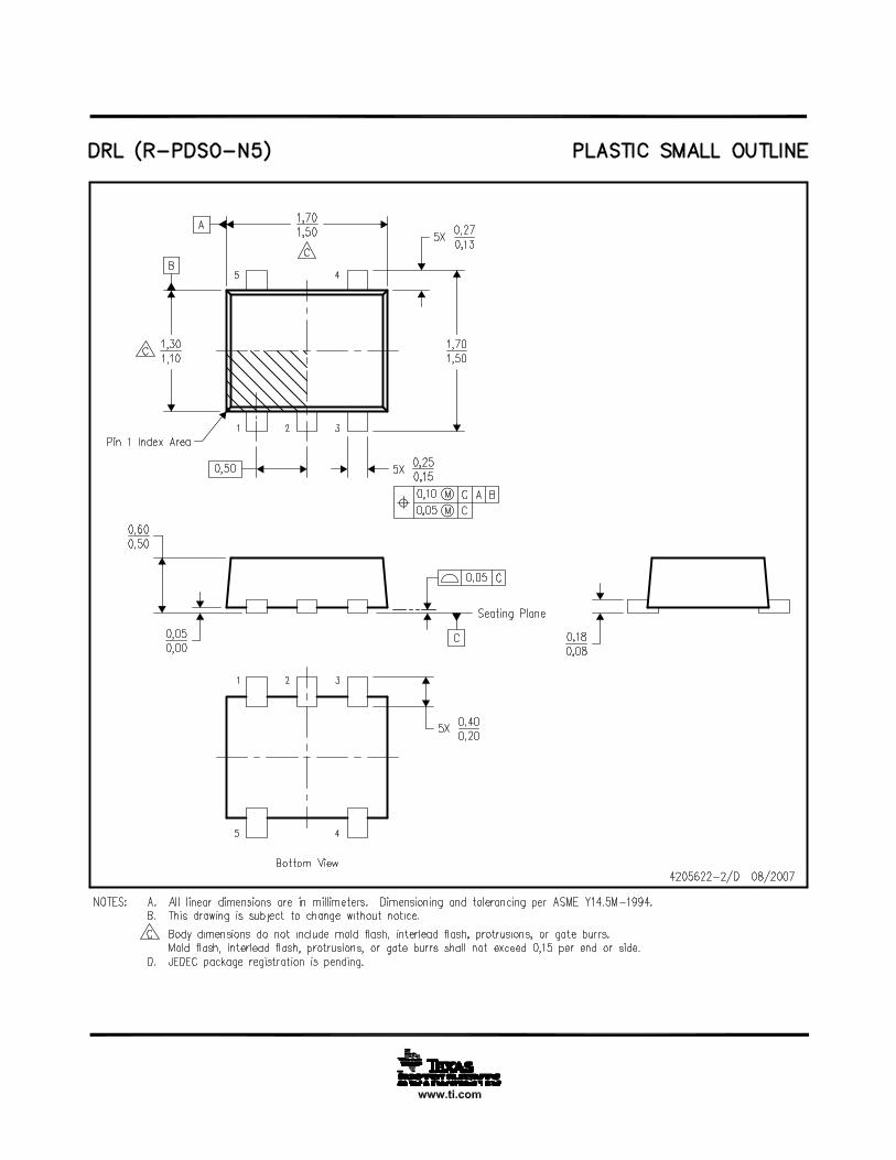
DCK PACKAGE(TOP VIEW)
3 4
2
Y
1
GND
A
N.C. 5 VCC
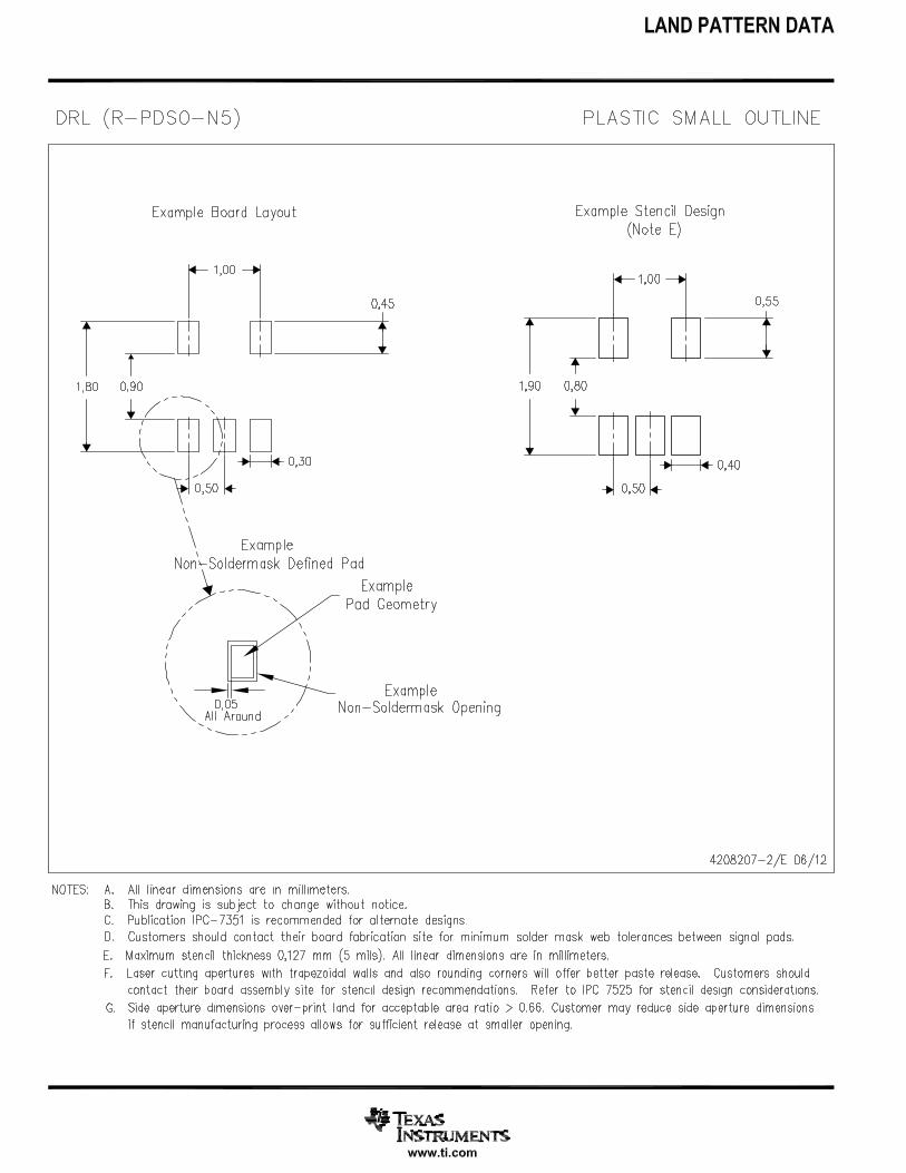
DRL PACKAGE(TOP VIEW)
2A
1N.C.
3 4GND Y
5 VCC
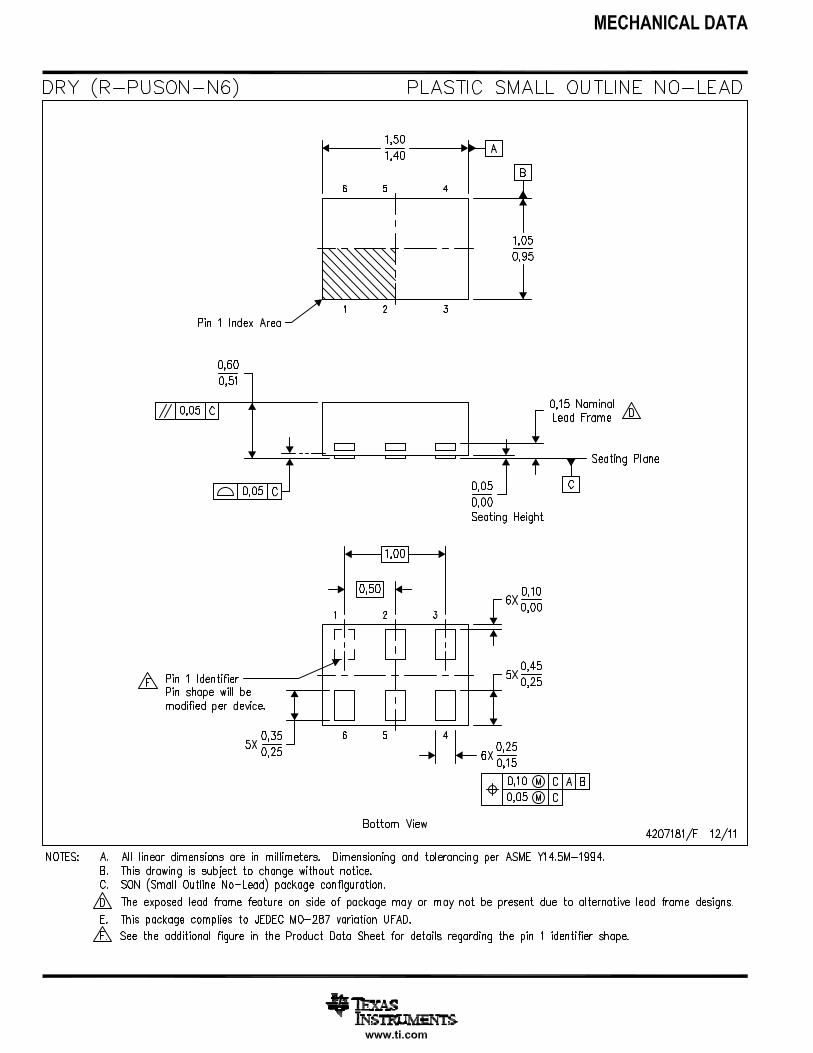
DRY PACKAGE(TOP VIEW)
A N.C.
N.C. 6
5
4
2
3GND Y
VCC1 N.C.
GND
DSF PACKAGE(TOP VIEW)
A
VCC
Y
N.C.
6
5
4
2
3
1
1 5
2
3
AGND
Y
VCC
DPW PACKAGE
(TOP VIEW)
N.C.
4
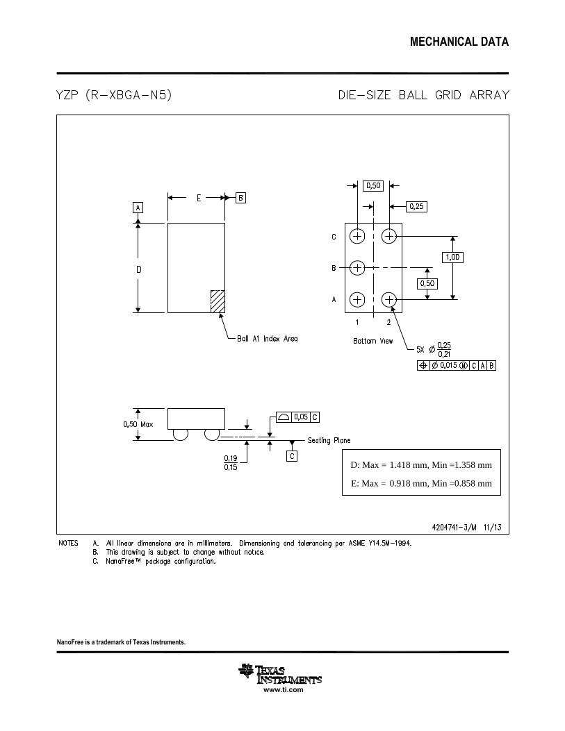
YZP PACKAGE
(TOP VIEW)
A
GND
DNU VCC
YC2C1
B1 B2
A1 A2
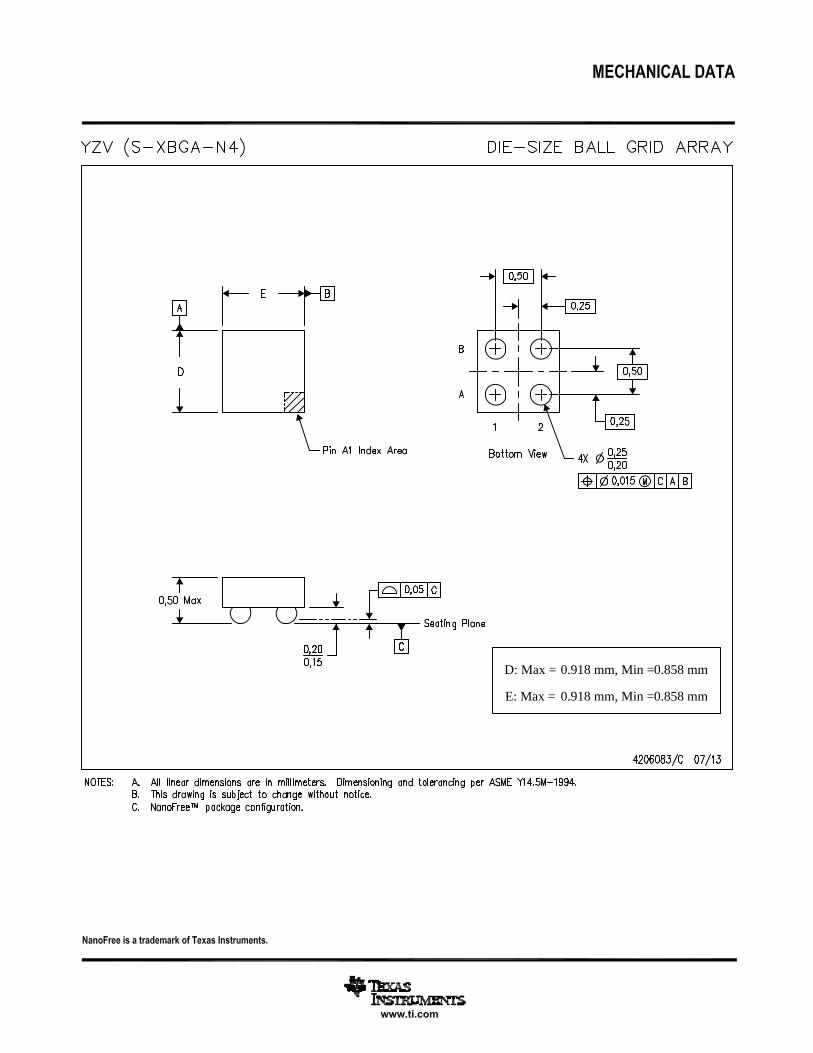
YZV PACKAGE
(TOP VIEW)
A
GND Y
VCCA1 A2
B1 B2
SN74LVC1G07SCES296AC –FEBRUARY 2000–REVISED APRIL 2014 www.ti.com
5 Pin Configuration and Functions
Pin FunctionsPIN
DESCRIPTIONDBV,NAME DRY, DSF DPW YZP YZVDCK, DRL
NC 1 1, 5 1 A1, B2 – Not connected
A 2 2 2 B1 A1 Input
GND 3 3 3 C1 B1 Ground
Y 4 4 4 C2 B2 Output
VCC 5 6 5 A2 A2 Power pin
6 Specifications
6.1 Absolute Maximum Ratingsover operating free-air temperature range (unless otherwise noted) (1)
MIN MAX UNITVCC Supply voltage range –0.5 6.5 VVI Input voltage range (2) –0.5 6.5 VVO Voltage range applied to any output in the high-impedance or power-off state (2) –0.5 6.5 VVO Voltage range applied to any output in the high or low state (2) (3) –0.5 6.5 VIIK Input clamp current VI < 0 –50 mAIOK Output clamp current VO < 0 –50 mAIO Continuous output current ±50 mA
Continuous current through VCC or GND ±100 mA
(1) Stresses beyond those listed under Absolute Maximum Ratings may cause permanent damage to the device. These are stress ratingsonly, and functional operation of the device at these or any other conditions beyond those indicated under Recommended OperatingConditions is not implied. Exposure to absolute-maximum-rated conditions for extended periods may affect device reliability.
(2) The input and output negative-voltage ratings may be exceeded if the input and output current ratings are observed.(3) The value of VCC is provided in the Recommended Operating Conditions table.
6.2 Handling RatingsMIN MAX UNIT
Tstg Storage temperature range –65 150 °CHuman body model (HBM), per ANSI/ESDA/JEDEC JS-001, all 0 2000pins (1)
V(ESD) Electrostatic discharge VCharged device model (CDM), per JEDEC specification 0 1000JESD22-C101, all pins (2)
(1) JEDEC document JEP155 states that 500-V HBM allows safe manufacturing with a standard ESD control process.(2) JEDEC document JEP157 states that 250-V CDM allows safe manufacturing with a standard ESD control process.
4 Submit Documentation Feedback Copyright © 2000–2014, Texas Instruments Incorporated
Product Folder Links: SN74LVC1G07
SN74LVC1G07www.ti.com SCES296AC –FEBRUARY 2000–REVISED APRIL 2014
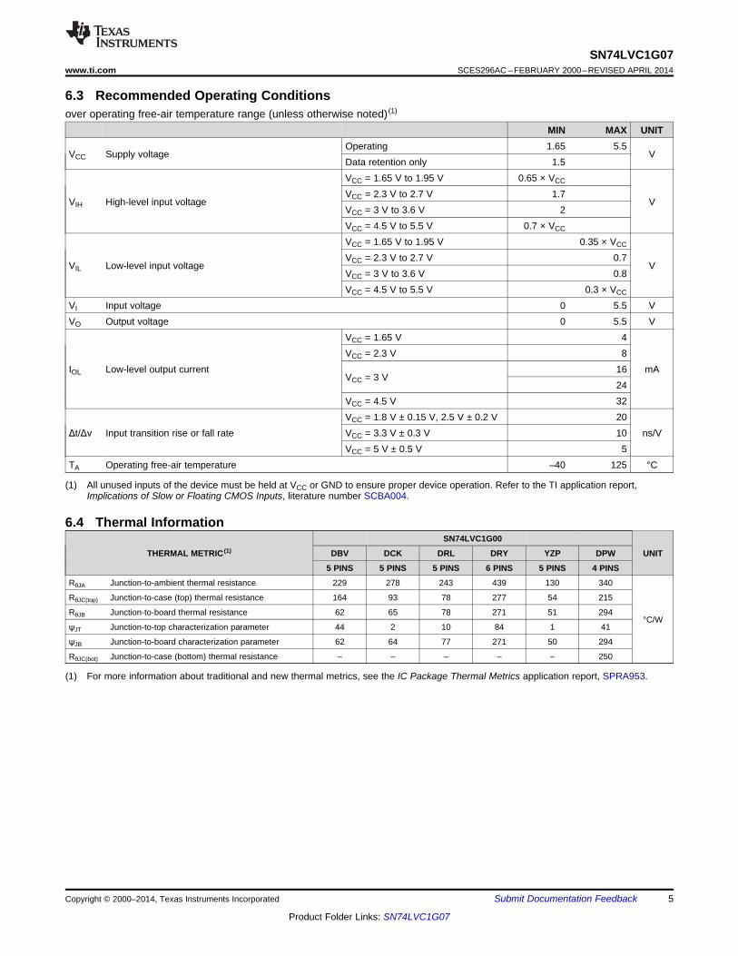
6.3 Recommended Operating Conditionsover operating free-air temperature range (unless otherwise noted) (1)
MIN MAX UNITOperating 1.65 5.5
VCC Supply voltage VData retention only 1.5VCC = 1.65 V to 1.95 V 0.65 × VCC
VCC = 2.3 V to 2.7 V 1.7VIH High-level input voltage V
VCC = 3 V to 3.6 V 2VCC = 4.5 V to 5.5 V 0.7 × VCC
VCC = 1.65 V to 1.95 V 0.35 × VCC
VCC = 2.3 V to 2.7 V 0.7VIL Low-level input voltage V
VCC = 3 V to 3.6 V 0.8VCC = 4.5 V to 5.5 V 0.3 × VCC
VI Input voltage 0 5.5 VVO Output voltage 0 5.5 V
VCC = 1.65 V 4VCC = 2.3 V 8
IOL Low-level output current 16 mAVCC = 3 V
24VCC = 4.5 V 32VCC = 1.8 V ± 0.15 V, 2.5 V ± 0.2 V 20
Δt/Δv Input transition rise or fall rate VCC = 3.3 V ± 0.3 V 10 ns/VVCC = 5 V ± 0.5 V 5
TA Operating free-air temperature –40 125 °C
(1) All unused inputs of the device must be held at VCC or GND to ensure proper device operation. Refer to the TI application report,Implications of Slow or Floating CMOS Inputs, literature number SCBA004.
6.4 Thermal InformationSN74LVC1G00
THERMAL METRIC (1) DBV DCK DRL DRY YZP DPW UNIT
5 PINS 5 PINS 5 PINS 6 PINS 5 PINS 4 PINS
RθJA Junction-to-ambient thermal resistance 229 278 243 439 130 340
RθJC(top) Junction-to-case (top) thermal resistance 164 93 78 277 54 215
RθJB Junction-to-board thermal resistance 62 65 78 271 51 294°C/W
ψJT Junction-to-top characterization parameter 44 2 10 84 1 41
ψJB Junction-to-board characterization parameter 62 64 77 271 50 294
RθJC(bot) Junction-to-case (bottom) thermal resistance – – – – – 250
(1) For more information about traditional and new thermal metrics, see the IC Package Thermal Metrics application report, SPRA953.
Copyright © 2000–2014, Texas Instruments Incorporated Submit Documentation Feedback 5
Product Folder Links: SN74LVC1G07
SN74LVC1G07SCES296AC –FEBRUARY 2000–REVISED APRIL 2014 www.ti.com
6.5 Electrical Characteristicsover recommended operating free-air temperature range (unless otherwise noted)
–40°C TO 125°C–40°C TO 85°C RECOMMENDEDPARAMETER TEST CONDITIONS VCC UNITTYP (1) MAX TYP MAX
IOL = 100 µA 1.65 V to 5.5 V 0.1 0.1
IOL = 4 mA 1.65 V 0.45 0.45
IOL = 8 mA 2.3 V 0.3 0.3VOL V
IOL = 16 mA 0.4 0.43 V
IOL = 24 mA 0.55 0.55
IOL = 32 mA 4.5 V 0.55 0.55
II A input VI = 5.5 V or GND 0 to 5.5 V ±5 ±5 µA
Ioff VI or VO = 5.5 V 0 ±10 ±10 µA
ICC VI = 5.5 V or GND, IO = 0 1.65 V to 5.5 V 10 10 µA
ΔICC One input at VCC – 0.6 V, Other inputs at VCC or GND 3 V to 5.5 V 500 500 µA
Ci VI = VCC or GND 3.3 V 4 4 pF
Co VO = VCC or GND 3.3 V 5 5 pF
(1) All typical values are at VCC = 3.3 V, TA = 25°C.
6.6 Switching Characteristics, –40°C to 85°Cover recommended operating free-air temperature range (unless otherwise noted) (see Figure 3)
–40°C TO 85°C
FROM TO VCC = 1.8 V VCC = 2.5 V VCC = 3.3 V VCC = 5 VPARAMETER UNIT(INPUT) (OUTPUT) ± 0.15 V ± 0.2 V ± 0.3 V ± 0.5 V
MIN MAX MIN MAX MIN MAX MIN MAX
tpd A Y 2.4 8.3 1 5.5 1.5 4.2 1 3.5 ns
6.7 Switching Characteristics, –40°C to 125°Cover recommended operating free-air temperature range (unless otherwise noted) (see Figure 3)
–40°C TO 125°CRECOMMENDED
FROM TOPARAMETER VCC = 1.8 V VCC = 2.5 V VCC = 3.3 V VCC = 5 V UNIT(INPUT) (OUTPUT) ± 0.15 V ± 0.2 V ± 0.3 V ± 0.5 V
MIN MAX MIN MAX MIN MAX MIN MAX
tpd A Y 2.4 8.6 1 6 1.5 4.7 1 4 ns
6.8 Operating CharacteristicsTA = 25°C
VCC = 1.8 V VCC = 2.5 V VCC = 3.3 V VCC = 5 VPARAMETER TEST CONDITIONS UNIT
TYP TYP TYP TYPCpd Power dissipation capacitance f = 10 MHz 3 3 4 6 pF
6 Submit Documentation Feedback Copyright © 2000–2014, Texas Instruments Incorporated
Product Folder Links: SN74LVC1G07
Temperature - °C
TPD
- ns
-100 -50 0 50 100 1500
0.5
1
1.5
2
2.5
D001
TPD
Vcc - V
TPD
- ns
0 1 2 3 4 5 60
1
2
3
4
5
6
D002
TPD
SN74LVC1G07www.ti.com SCES296AC –FEBRUARY 2000–REVISED APRIL 2014
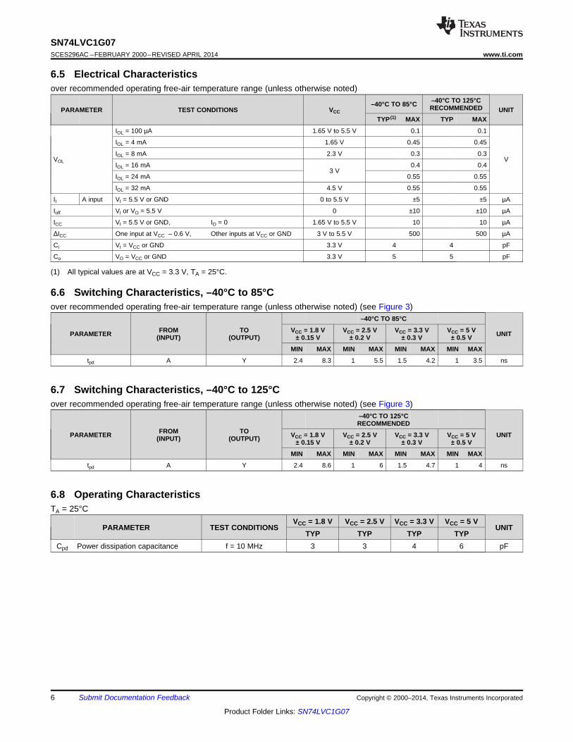
6.9 Typical Characteristics
Figure 1. TPD Across Temperature at 3.3V Vcc Figure 2. TPD Across Vcc at 25°C
Copyright © 2000–2014, Texas Instruments Incorporated Submit Documentation Feedback 7
Product Folder Links: SN74LVC1G07
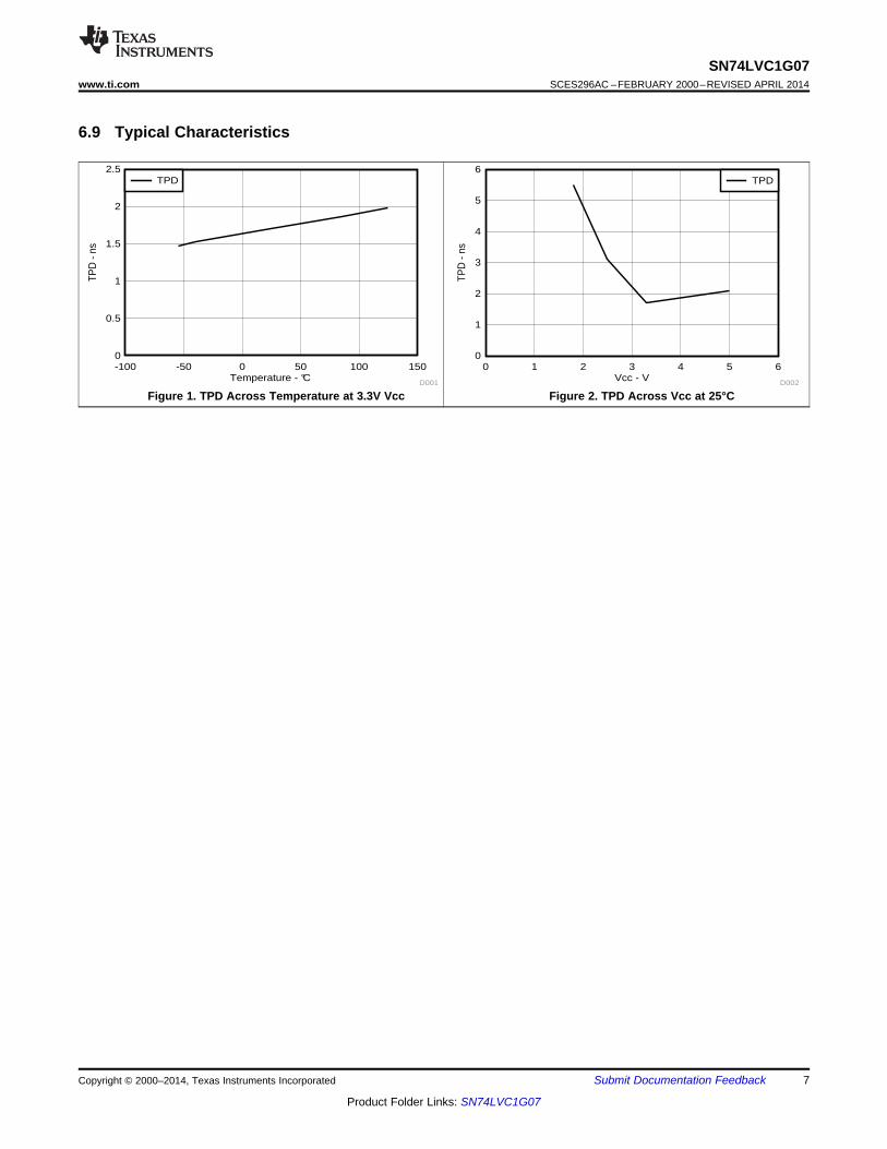
VM
thtsu
From OutputUnder Test
CL(see Note A)
LOAD CIRCUIT
S1VLOAD
Open
GNDRL
RL
Data Input
Timing InputVI
0 V
VI
0 V0 V
tw
Input
VOLTAGE WAVEFORMSSETUP AND HOLD TIMES
VOLTAGE WAVEFORMSPROPAGATION DELAY TIMES
INVERTING AND NONINVERTING OUTPUTS
VOLTAGE WAVEFORMSPULSE DURATION
tPLH
tPHL
tPHL
tPLH
VOH
VOH
VOL
VOL
VI
0 VInput
OutputWaveform 1S1 at VLOAD(see Note B)
OutputWaveform 2S1 at VLOAD(see Note B)
VOL
tPZL
tPZH
tPLZ
tPHZ
VLOAD/2
0 V
VOL + V∆
VLOAD/2 − V∆
≈0 V
VI
VOLTAGE WAVEFORMSENABLE AND DISABLE TIMES
LOW- AND HIGH-LEVEL ENABLING
Output
Output
NOTES: A. CL includes probe and jig capacitance.B. Waveform 1 is for an output with internal conditions such that the output is low, except when disabled by the output control.
Waveform 2 is for an output with internal conditions such that the output is high, except when disabled by the output control.C. All input pulses are supplied by generators having the following characteristics: PRR ≤ 10 MHz, ZO = 50 Ω.D. The outputs are measured one at a time, with one transition per measurement.E. Since this device has open-drain outputs, tPLZ and tPZL are the same as tpd.F. tPZL is measured at VM.G. tPLZ is measured at VOL + V∆.H. All parameters and waveforms are not applicable to all devices.
OutputControl
VM VM
VM VM
VM VM
VM
VM VM
VM
VM
VM
VI
VM
VM
1.8 V ± 0.15 V2.5 V ± 0.2 V3.3 V ± 0.3 V5 V ± 0.5 V
1 kΩ500 Ω500 Ω500 Ω
VCC RL
2 × VCC2 × VCC
6 V2 × VCC
VLOAD CL
30 pF30 pF50 pF50 pF
0.15 V0.15 V0.3 V0.3 V
V∆
VCCVCC3 VVCC
VI
VCC/2VCC/21.5 VVCC/2
VMtr/tf
≤ 2 ns≤ 2 ns
≤ 2.5 ns≤ 2.5 ns
INPUT
tPZL (see Notes E and F)
tPLZ (see Notes E and G)
tPHZ/tPZH
VLOAD
VLOAD
VLOAD
TEST S1
VLOAD/2
SN74LVC1G07SCES296AC –FEBRUARY 2000–REVISED APRIL 2014 www.ti.com
7 Parameter Measurement Information
7.1 (Open Drain)
Figure 3. Load Circuit and Voltage Waveforms
8 Submit Documentation Feedback Copyright © 2000–2014, Texas Instruments Incorporated
Product Folder Links: SN74LVC1G07
A Y
SN74LVC1G07www.ti.com SCES296AC –FEBRUARY 2000–REVISED APRIL 2014
8 Detailed Description
8.1 OverviewThe SN74LVC1G07 device contains one open drain buffer with a maximum sink current of 32 mA. This device isfully specified for partial-power-down applications using Ioff. The Ioff circuitry disables the outputs, preventingdamaging current backflow through the device when it is powered down.
The DPW package technology is a major breakthrough in IC packaging. Its tiny 0.64 mm square footprint savessignificant board space over other package options while still retaining the traditional manufacturing friendly leadpitch of 0.5 mm.
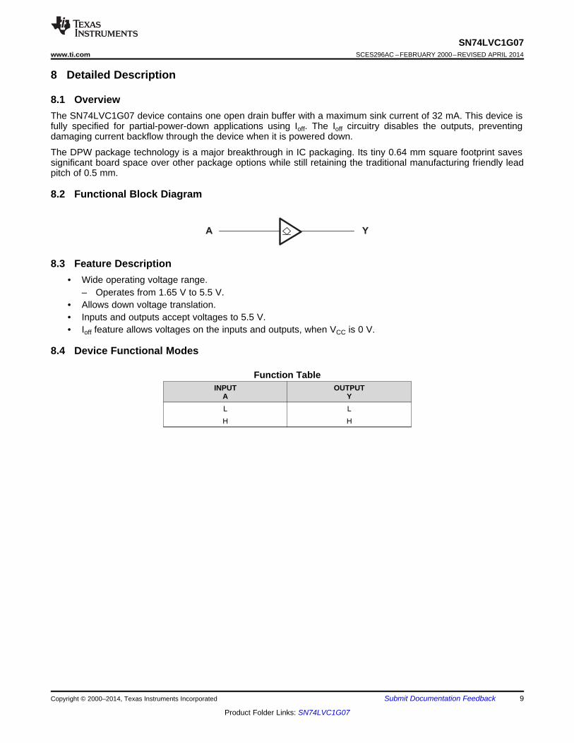
8.2 Functional Block Diagram
8.3 Feature Description• Wide operating voltage range.
– Operates from 1.65 V to 5.5 V.• Allows down voltage translation.• Inputs and outputs accept voltages to 5.5 V.• Ioff feature allows voltages on the inputs and outputs, when VCC is 0 V.
8.4 Device Functional Modes
Function TableINPUT OUTPUT
A YL LH H
Copyright © 2000–2014, Texas Instruments Incorporated Submit Documentation Feedback 9
Product Folder Links: SN74LVC1G07
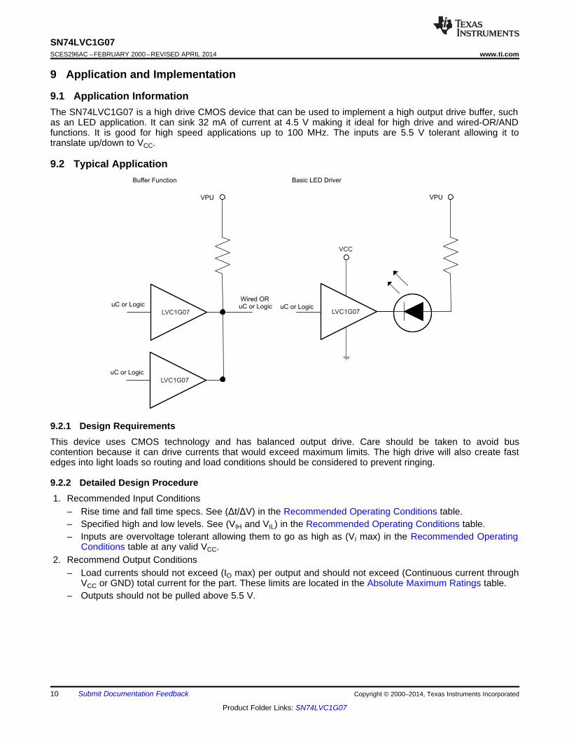
uC or Logic
Basic LED Driver
Wired ORuC or Logic
Buffer Function
uC or Logic
VPU
uC or Logic
VPU
LVC1G07
LVC1G07
LVC1G07
VCC
SN74LVC1G07SCES296AC –FEBRUARY 2000–REVISED APRIL 2014 www.ti.com
9 Application and Implementation
9.1 Application InformationThe SN74LVC1G07 is a high drive CMOS device that can be used to implement a high output drive buffer, suchas an LED application. It can sink 32 mA of current at 4.5 V making it ideal for high drive and wired-OR/ANDfunctions. It is good for high speed applications up to 100 MHz. The inputs are 5.5 V tolerant allowing it totranslate up/down to VCC.
9.2 Typical Application
9.2.1 Design RequirementsThis device uses CMOS technology and has balanced output drive. Care should be taken to avoid buscontention because it can drive currents that would exceed maximum limits. The high drive will also create fastedges into light loads so routing and load conditions should be considered to prevent ringing.
9.2.2 Detailed Design Procedure1. Recommended Input Conditions
– Rise time and fall time specs. See (Δt/ΔV) in the Recommended Operating Conditions table.– Specified high and low levels. See (VIH and VIL) in the Recommended Operating Conditions table.– Inputs are overvoltage tolerant allowing them to go as high as (VI max) in the Recommended Operating
Conditions table at any valid VCC.2. Recommend Output Conditions
– Load currents should not exceed (IO max) per output and should not exceed (Continuous current throughVCC or GND) total current for the part. These limits are located in the Absolute Maximum Ratings table.
– Outputs should not be pulled above 5.5 V.
10 Submit Documentation Feedback Copyright © 2000–2014, Texas Instruments Incorporated
Product Folder Links: SN74LVC1G07
VCC
Unused Input
Input
Output Output
Input
Unused Input
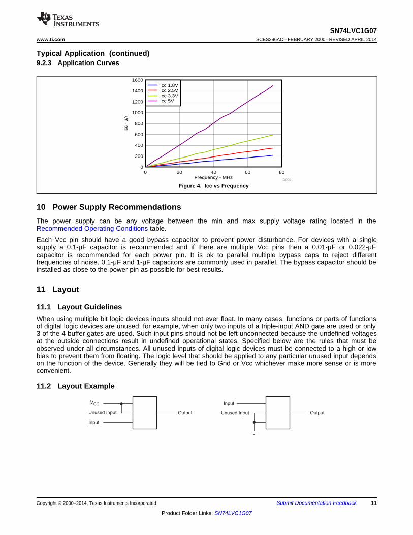
Frequency - MHz
Icc
- µA
0 20 40 60 800
200
400
600
800
1000
1200
1400
1600
D001
Icc 1.8VIcc 2.5VIcc 3.3VIcc 5V
SN74LVC1G07www.ti.com SCES296AC –FEBRUARY 2000–REVISED APRIL 2014
Typical Application (continued)9.2.3 Application Curves
Figure 4. Icc vs Frequency
10 Power Supply RecommendationsThe power supply can be any voltage between the min and max supply voltage rating located in theRecommended Operating Conditions table.
Each Vcc pin should have a good bypass capacitor to prevent power disturbance. For devices with a singlesupply a 0.1-μF capacitor is recommended and if there are multiple Vcc pins then a 0.01-μF or 0.022-μFcapacitor is recommended for each power pin. It is ok to parallel multiple bypass caps to reject differentfrequencies of noise. 0.1-μF and 1-μF capacitors are commonly used in parallel. The bypass capacitor should beinstalled as close to the power pin as possible for best results.
11 Layout
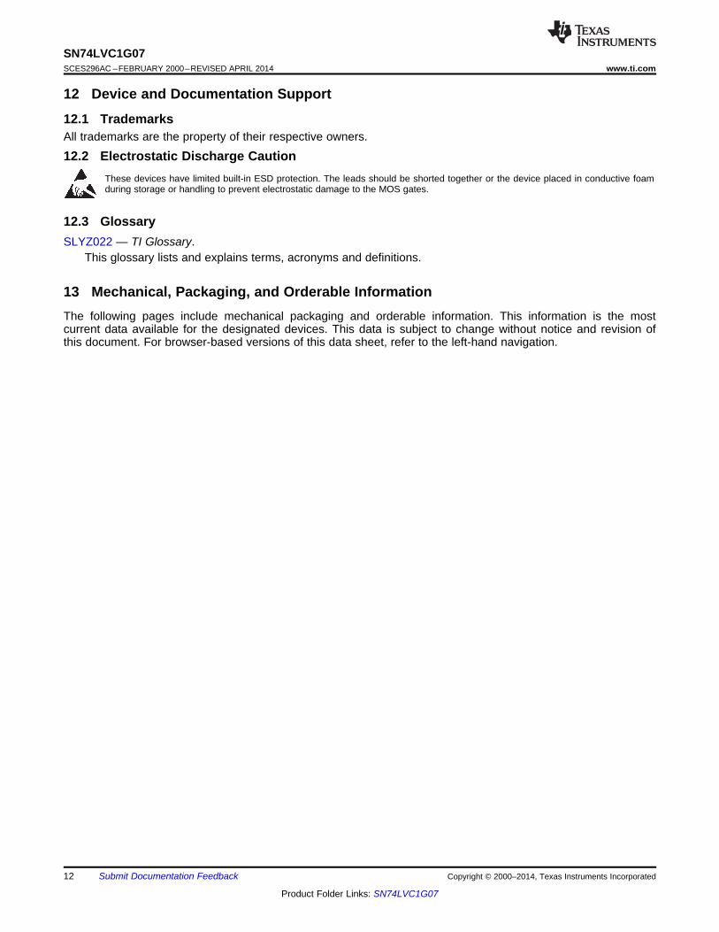
11.1 Layout GuidelinesWhen using multiple bit logic devices inputs should not ever float. In many cases, functions or parts of functionsof digital logic devices are unused; for example, when only two inputs of a triple-input AND gate are used or only3 of the 4 buffer gates are used. Such input pins should not be left unconnected because the undefined voltagesat the outside connections result in undefined operational states. Specified below are the rules that must beobserved under all circumstances. All unused inputs of digital logic devices must be connected to a high or lowbias to prevent them from floating. The logic level that should be applied to any particular unused input dependson the function of the device. Generally they will be tied to Gnd or Vcc whichever make more sense or is moreconvenient.
11.2 Layout Example
Copyright © 2000–2014, Texas Instruments Incorporated Submit Documentation Feedback 11
Product Folder Links: SN74LVC1G07
SN74LVC1G07SCES296AC –FEBRUARY 2000–REVISED APRIL 2014 www.ti.com
12 Device and Documentation Support
12.1 TrademarksAll trademarks are the property of their respective owners.
12.2 Electrostatic Discharge CautionThese devices have limited built-in ESD protection. The leads should be shorted together or the device placed in conductive foamduring storage or handling to prevent electrostatic damage to the MOS gates.
12.3 GlossarySLYZ022 — TI Glossary.
This glossary lists and explains terms, acronyms and definitions.
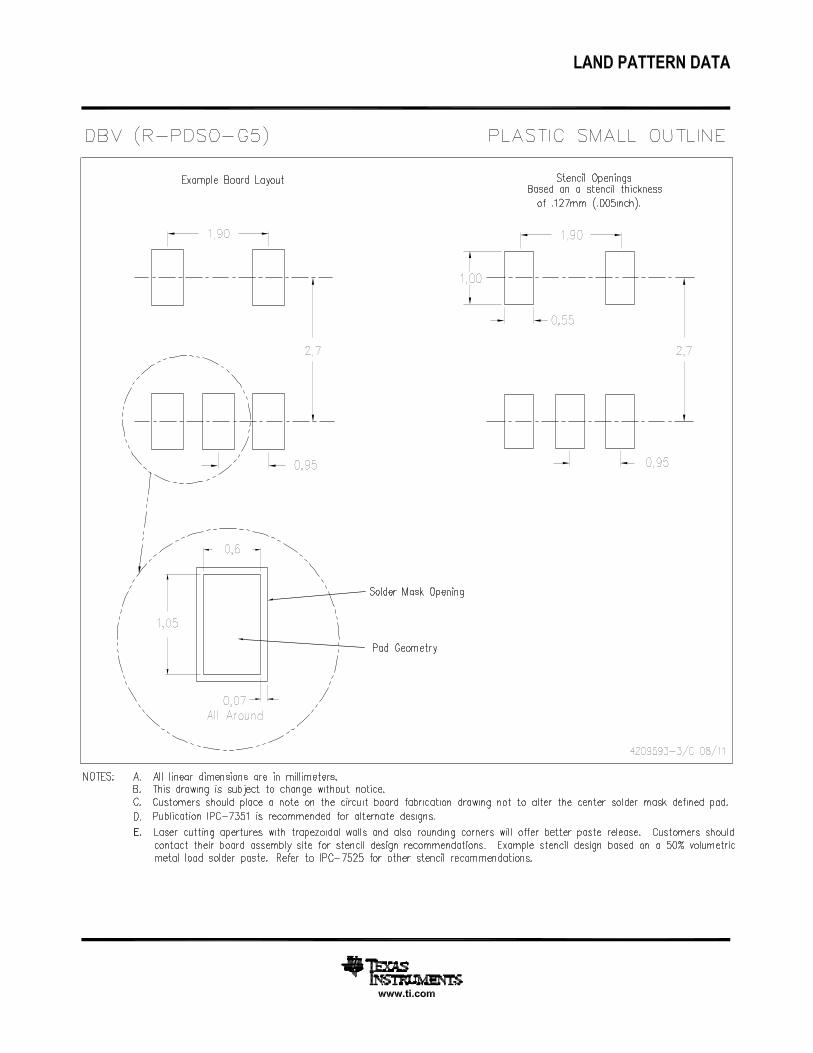
13 Mechanical, Packaging, and Orderable InformationThe following pages include mechanical packaging and orderable information. This information is the mostcurrent data available for the designated devices. This data is subject to change without notice and revision ofthis document. For browser-based versions of this data sheet, refer to the left-hand navigation.
12 Submit Documentation Feedback Copyright © 2000–2014, Texas Instruments Incorporated
Product Folder Links: SN74LVC1G07
PACKAGE OPTION ADDENDUM
www.ti.com 17-May-2014
Addendum-Page 1
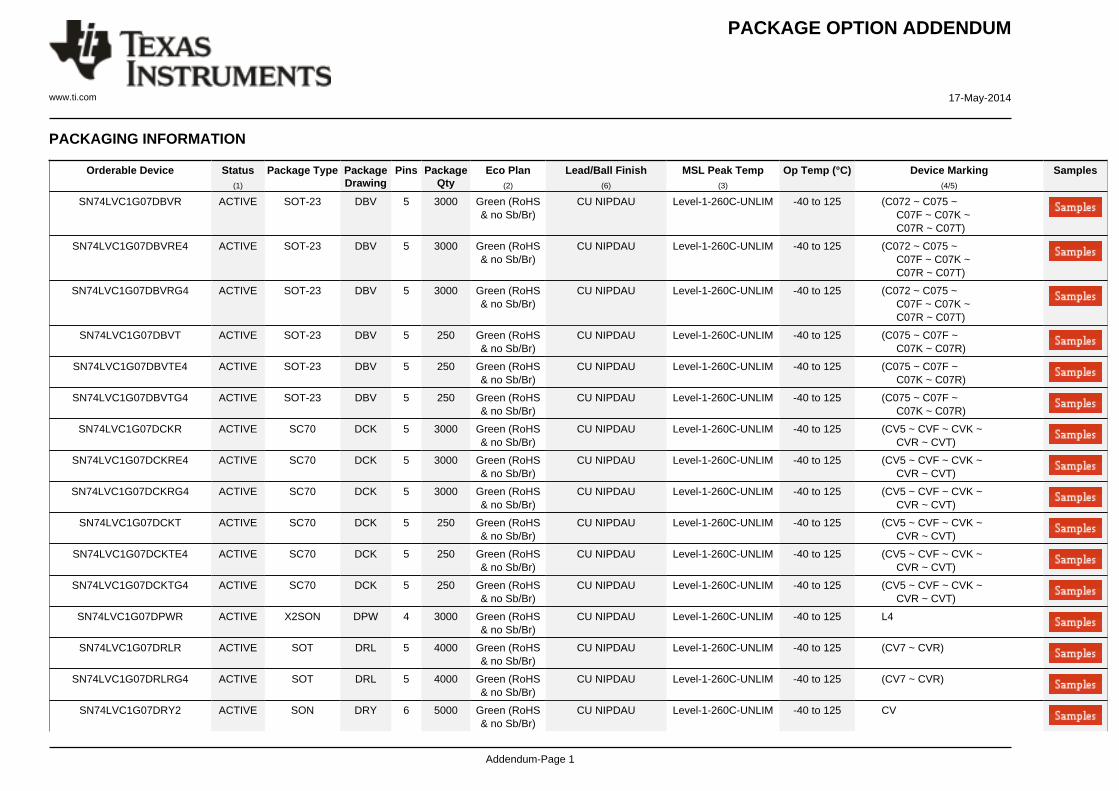
PACKAGING INFORMATION
Orderable Device Status(1)
Package Type PackageDrawing
Pins PackageQty
Eco Plan(2)
Lead/Ball Finish(6)
MSL Peak Temp(3)
Op Temp (°C) Device Marking(4/5)
Samples
SN74LVC1G07DBVR ACTIVE SOT-23 DBV 5 3000 Green (RoHS& no Sb/Br)
CU NIPDAU Level-1-260C-UNLIM -40 to 125 (C072 ~ C075 ~ C07F ~ C07K ~ C07R ~ C07T)
SN74LVC1G07DBVRE4 ACTIVE SOT-23 DBV 5 3000 Green (RoHS& no Sb/Br)
CU NIPDAU Level-1-260C-UNLIM -40 to 125 (C072 ~ C075 ~ C07F ~ C07K ~ C07R ~ C07T)
SN74LVC1G07DBVRG4 ACTIVE SOT-23 DBV 5 3000 Green (RoHS& no Sb/Br)
CU NIPDAU Level-1-260C-UNLIM -40 to 125 (C072 ~ C075 ~ C07F ~ C07K ~ C07R ~ C07T)
SN74LVC1G07DBVT ACTIVE SOT-23 DBV 5 250 Green (RoHS& no Sb/Br)
CU NIPDAU Level-1-260C-UNLIM -40 to 125 (C075 ~ C07F ~ C07K ~ C07R)
SN74LVC1G07DBVTE4 ACTIVE SOT-23 DBV 5 250 Green (RoHS& no Sb/Br)
CU NIPDAU Level-1-260C-UNLIM -40 to 125 (C075 ~ C07F ~ C07K ~ C07R)
SN74LVC1G07DBVTG4 ACTIVE SOT-23 DBV 5 250 Green (RoHS& no Sb/Br)
CU NIPDAU Level-1-260C-UNLIM -40 to 125 (C075 ~ C07F ~ C07K ~ C07R)
SN74LVC1G07DCKR ACTIVE SC70 DCK 5 3000 Green (RoHS& no Sb/Br)
CU NIPDAU Level-1-260C-UNLIM -40 to 125 (CV5 ~ CVF ~ CVK ~ CVR ~ CVT)
SN74LVC1G07DCKRE4 ACTIVE SC70 DCK 5 3000 Green (RoHS& no Sb/Br)
CU NIPDAU Level-1-260C-UNLIM -40 to 125 (CV5 ~ CVF ~ CVK ~ CVR ~ CVT)
SN74LVC1G07DCKRG4 ACTIVE SC70 DCK 5 3000 Green (RoHS& no Sb/Br)
CU NIPDAU Level-1-260C-UNLIM -40 to 125 (CV5 ~ CVF ~ CVK ~ CVR ~ CVT)
SN74LVC1G07DCKT ACTIVE SC70 DCK 5 250 Green (RoHS& no Sb/Br)
CU NIPDAU Level-1-260C-UNLIM -40 to 125 (CV5 ~ CVF ~ CVK ~ CVR ~ CVT)
SN74LVC1G07DCKTE4 ACTIVE SC70 DCK 5 250 Green (RoHS& no Sb/Br)
CU NIPDAU Level-1-260C-UNLIM -40 to 125 (CV5 ~ CVF ~ CVK ~ CVR ~ CVT)
SN74LVC1G07DCKTG4 ACTIVE SC70 DCK 5 250 Green (RoHS& no Sb/Br)
CU NIPDAU Level-1-260C-UNLIM -40 to 125 (CV5 ~ CVF ~ CVK ~ CVR ~ CVT)
SN74LVC1G07DPWR ACTIVE X2SON DPW 4 3000 Green (RoHS& no Sb/Br)
CU NIPDAU Level-1-260C-UNLIM -40 to 125 L4
SN74LVC1G07DRLR ACTIVE SOT DRL 5 4000 Green (RoHS& no Sb/Br)
CU NIPDAU Level-1-260C-UNLIM -40 to 125 (CV7 ~ CVR)
SN74LVC1G07DRLRG4 ACTIVE SOT DRL 5 4000 Green (RoHS& no Sb/Br)
CU NIPDAU Level-1-260C-UNLIM -40 to 125 (CV7 ~ CVR)
SN74LVC1G07DRY2 ACTIVE SON DRY 6 5000 Green (RoHS& no Sb/Br)
CU NIPDAU Level-1-260C-UNLIM -40 to 125 CV

PACKAGE OPTION ADDENDUM
www.ti.com 17-May-2014
Addendum-Page 2
Orderable Device Status(1)
Package Type PackageDrawing
Pins PackageQty
Eco Plan(2)
Lead/Ball Finish(6)
MSL Peak Temp(3)
Op Temp (°C) Device Marking(4/5)
Samples
SN74LVC1G07DRYR ACTIVE SON DRY 6 5000 Green (RoHS& no Sb/Br)
CU NIPDAU Level-1-260C-UNLIM -40 to 125 CV
SN74LVC1G07DRYRG4 ACTIVE SON DRY 6 5000 Green (RoHS& no Sb/Br)
CU NIPDAU Level-1-260C-UNLIM -40 to 125 CV
SN74LVC1G07DSF2 ACTIVE SON DSF 6 5000 Green (RoHS& no Sb/Br)
CU NIPDAU Level-1-260C-UNLIM -40 to 125 CV
SN74LVC1G07DSFR ACTIVE SON DSF 6 5000 Green (RoHS& no Sb/Br)
CU NIPDAU Level-1-260C-UNLIM -40 to 125 CV
SN74LVC1G07YZPR ACTIVE DSBGA YZP 5 3000 Green (RoHS& no Sb/Br)
SNAGCU Level-1-260C-UNLIM -40 to 125 (CV7 ~ CVN)
SN74LVC1G07YZVR ACTIVE DSBGA YZV 4 3000 Green (RoHS& no Sb/Br)
SNAGCU Level-1-260C-UNLIM -40 to 85 CV(7 ~ N)
(1) The marketing status values are defined as follows:ACTIVE: Product device recommended for new designs.LIFEBUY: TI has announced that the device will be discontinued, and a lifetime-buy period is in effect.NRND: Not recommended for new designs. Device is in production to support existing customers, but TI does not recommend using this part in a new design.PREVIEW: Device has been announced but is not in production. Samples may or may not be available.OBSOLETE: TI has discontinued the production of the device.
(2) Eco Plan - The planned eco-friendly classification: Pb-Free (RoHS), Pb-Free (RoHS Exempt), or Green (RoHS & no Sb/Br) - please check http://www.ti.com/productcontent for the latest availabilityinformation and additional product content details.TBD: The Pb-Free/Green conversion plan has not been defined.Pb-Free (RoHS): TI's terms "Lead-Free" or "Pb-Free" mean semiconductor products that are compatible with the current RoHS requirements for all 6 substances, including the requirement thatlead not exceed 0.1% by weight in homogeneous materials. Where designed to be soldered at high temperatures, TI Pb-Free products are suitable for use in specified lead-free processes.Pb-Free (RoHS Exempt): This component has a RoHS exemption for either 1) lead-based flip-chip solder bumps used between the die and package, or 2) lead-based die adhesive used betweenthe die and leadframe. The component is otherwise considered Pb-Free (RoHS compatible) as defined above.Green (RoHS & no Sb/Br): TI defines "Green" to mean Pb-Free (RoHS compatible), and free of Bromine (Br) and Antimony (Sb) based flame retardants (Br or Sb do not exceed 0.1% by weightin homogeneous material)
(3) MSL, Peak Temp. - The Moisture Sensitivity Level rating according to the JEDEC industry standard classifications, and peak solder temperature.
(4) There may be additional marking, which relates to the logo, the lot trace code information, or the environmental category on the device.
(5) Multiple Device Markings will be inside parentheses. Only one Device Marking contained in parentheses and separated by a "~" will appear on a device. If a line is indented then it is a continuationof the previous line and the two combined represent the entire Device Marking for that device.
PACKAGE OPTION ADDENDUM
www.ti.com 17-May-2014
Addendum-Page 3
(6) Lead/Ball Finish - Orderable Devices may have multiple material finish options. Finish options are separated by a vertical ruled line. Lead/Ball Finish values may wrap to two lines if the finishvalue exceeds the maximum column width.
Important Information and Disclaimer:The information provided on this page represents TI's knowledge and belief as of the date that it is provided. TI bases its knowledge and belief on informationprovided by third parties, and makes no representation or warranty as to the accuracy of such information. Efforts are underway to better integrate information from third parties. TI has taken andcontinues to take reasonable steps to provide representative and accurate information but may not have conducted destructive testing or chemical analysis on incoming materials and chemicals.TI and TI suppliers consider certain information to be proprietary, and thus CAS numbers and other limited information may not be available for release.
In no event shall TI's liability arising out of such information exceed the total purchase price of the TI part(s) at issue in this document sold by TI to Customer on an annual basis.
OTHER QUALIFIED VERSIONS OF SN74LVC1G07 :
• Automotive: SN74LVC1G07-Q1
• Enhanced Product: SN74LVC1G07-EP
NOTE: Qualified Version Definitions:
• Automotive - Q100 devices qualified for high-reliability automotive applications targeting zero defects
• Enhanced Product - Supports Defense, Aerospace and Medical Applications
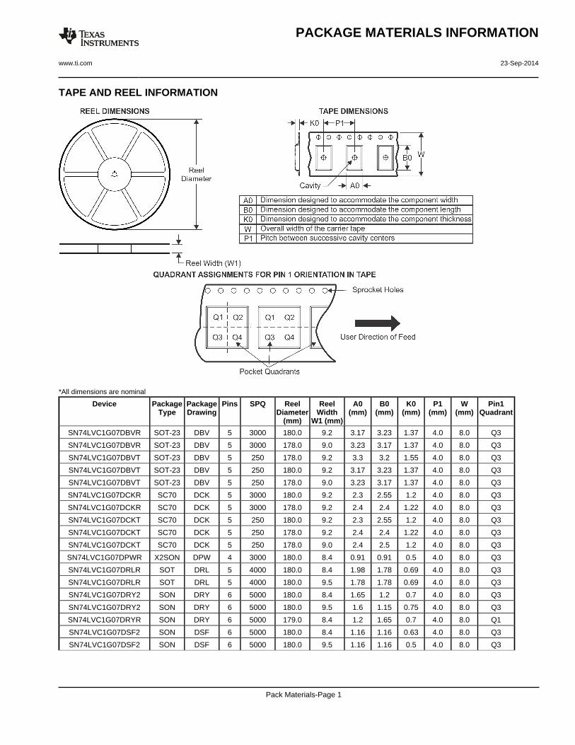
TAPE AND REEL INFORMATION
*All dimensions are nominal
Device PackageType
PackageDrawing
Pins SPQ ReelDiameter
(mm)
ReelWidth
W1 (mm)
A0(mm)
B0(mm)
K0(mm)
P1(mm)
W(mm)
Pin1Quadrant
SN74LVC1G07DBVR SOT-23 DBV 5 3000 180.0 9.2 3.17 3.23 1.37 4.0 8.0 Q3
SN74LVC1G07DBVR SOT-23 DBV 5 3000 178.0 9.0 3.23 3.17 1.37 4.0 8.0 Q3
SN74LVC1G07DBVT SOT-23 DBV 5 250 178.0 9.2 3.3 3.2 1.55 4.0 8.0 Q3
SN74LVC1G07DBVT SOT-23 DBV 5 250 180.0 9.2 3.17 3.23 1.37 4.0 8.0 Q3
SN74LVC1G07DBVT SOT-23 DBV 5 250 178.0 9.0 3.23 3.17 1.37 4.0 8.0 Q3
SN74LVC1G07DCKR SC70 DCK 5 3000 180.0 9.2 2.3 2.55 1.2 4.0 8.0 Q3
SN74LVC1G07DCKR SC70 DCK 5 3000 178.0 9.2 2.4 2.4 1.22 4.0 8.0 Q3
SN74LVC1G07DCKT SC70 DCK 5 250 180.0 9.2 2.3 2.55 1.2 4.0 8.0 Q3
SN74LVC1G07DCKT SC70 DCK 5 250 178.0 9.2 2.4 2.4 1.22 4.0 8.0 Q3
SN74LVC1G07DCKT SC70 DCK 5 250 178.0 9.0 2.4 2.5 1.2 4.0 8.0 Q3
SN74LVC1G07DPWR X2SON DPW 4 3000 180.0 8.4 0.91 0.91 0.5 4.0 8.0 Q3
SN74LVC1G07DRLR SOT DRL 5 4000 180.0 8.4 1.98 1.78 0.69 4.0 8.0 Q3
SN74LVC1G07DRLR SOT DRL 5 4000 180.0 9.5 1.78 1.78 0.69 4.0 8.0 Q3
SN74LVC1G07DRY2 SON DRY 6 5000 180.0 8.4 1.65 1.2 0.7 4.0 8.0 Q3
SN74LVC1G07DRY2 SON DRY 6 5000 180.0 9.5 1.6 1.15 0.75 4.0 8.0 Q3
SN74LVC1G07DRYR SON DRY 6 5000 179.0 8.4 1.2 1.65 0.7 4.0 8.0 Q1
SN74LVC1G07DSF2 SON DSF 6 5000 180.0 8.4 1.16 1.16 0.63 4.0 8.0 Q3
SN74LVC1G07DSF2 SON DSF 6 5000 180.0 9.5 1.16 1.16 0.5 4.0 8.0 Q3
PACKAGE MATERIALS INFORMATION
www.ti.com 23-Sep-2014
Pack Materials-Page 1
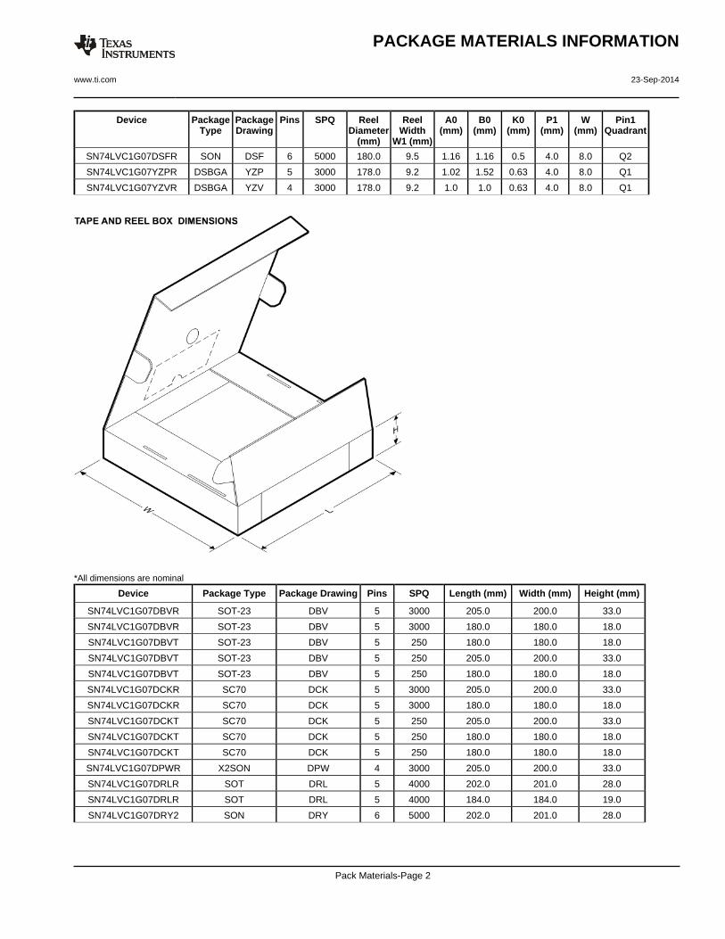
Device PackageType
PackageDrawing
Pins SPQ ReelDiameter
(mm)
ReelWidth
W1 (mm)
A0(mm)
B0(mm)
K0(mm)
P1(mm)
W(mm)
Pin1Quadrant
SN74LVC1G07DSFR SON DSF 6 5000 180.0 9.5 1.16 1.16 0.5 4.0 8.0 Q2
SN74LVC1G07YZPR DSBGA YZP 5 3000 178.0 9.2 1.02 1.52 0.63 4.0 8.0 Q1
SN74LVC1G07YZVR DSBGA YZV 4 3000 178.0 9.2 1.0 1.0 0.63 4.0 8.0 Q1
*All dimensions are nominal
Device Package Type Package Drawing Pins SPQ Length (mm) Width (mm) Height (mm)
SN74LVC1G07DBVR SOT-23 DBV 5 3000 205.0 200.0 33.0
SN74LVC1G07DBVR SOT-23 DBV 5 3000 180.0 180.0 18.0
SN74LVC1G07DBVT SOT-23 DBV 5 250 180.0 180.0 18.0
SN74LVC1G07DBVT SOT-23 DBV 5 250 205.0 200.0 33.0
SN74LVC1G07DBVT SOT-23 DBV 5 250 180.0 180.0 18.0
SN74LVC1G07DCKR SC70 DCK 5 3000 205.0 200.0 33.0
SN74LVC1G07DCKR SC70 DCK 5 3000 180.0 180.0 18.0
SN74LVC1G07DCKT SC70 DCK 5 250 205.0 200.0 33.0
SN74LVC1G07DCKT SC70 DCK 5 250 180.0 180.0 18.0
SN74LVC1G07DCKT SC70 DCK 5 250 180.0 180.0 18.0
SN74LVC1G07DPWR X2SON DPW 4 3000 205.0 200.0 33.0
SN74LVC1G07DRLR SOT DRL 5 4000 202.0 201.0 28.0
SN74LVC1G07DRLR SOT DRL 5 4000 184.0 184.0 19.0
SN74LVC1G07DRY2 SON DRY 6 5000 202.0 201.0 28.0
PACKAGE MATERIALS INFORMATION
www.ti.com 23-Sep-2014
Pack Materials-Page 2
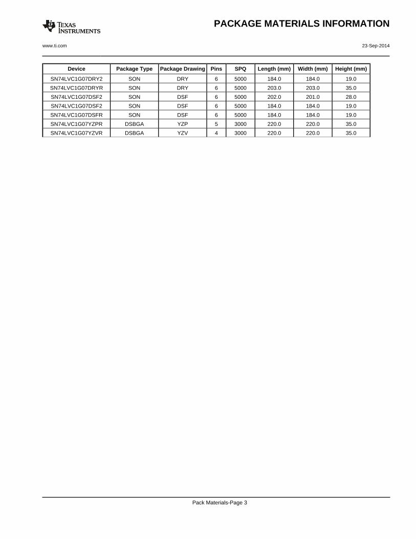
Device Package Type Package Drawing Pins SPQ Length (mm) Width (mm) Height (mm)
SN74LVC1G07DRY2 SON DRY 6 5000 184.0 184.0 19.0
SN74LVC1G07DRYR SON DRY 6 5000 203.0 203.0 35.0
SN74LVC1G07DSF2 SON DSF 6 5000 202.0 201.0 28.0
SN74LVC1G07DSF2 SON DSF 6 5000 184.0 184.0 19.0
SN74LVC1G07DSFR SON DSF 6 5000 184.0 184.0 19.0
SN74LVC1G07YZPR DSBGA YZP 5 3000 220.0 220.0 35.0
SN74LVC1G07YZVR DSBGA YZV 4 3000 220.0 220.0 35.0
PACKAGE MATERIALS INFORMATION
www.ti.com 23-Sep-2014
Pack Materials-Page 3
www.ti.com
C
6X 0.220.12
6X 0.450.35
2X0.7
4X0.35
0.4 MAX
0.050.00
A 1.050.95 B
1.050.95
(0.11) TYP
(0.1)PIN 1 ID
4208186/F 10/2014
PIN 1 INDEX AREA
SEATING PLANE
0.05 C
1
34
6
0.07 C A B0.05 C
SYMM
SYMM
NOTES: 1. All linear dimensions are in millimeters. Any dimensions in parenthesis are for reference only. Dimensioning and tolerancing per ASME Y14.5M. 2. This drawing is subject to change without notice.3. Reference JEDEC registration MO-287, variation X2AAF.
MECHANICAL DATA
DSF (S-PX2SON-N6) PLASTIC SMALL OUTLINE NO-LEAD
D: Max =
E: Max =
1.418 mm, Min =
0.918 mm, Min =
1.358 mm
0.858 mm
D: Max =
E: Max =
0.918 mm, Min =
0.918 mm, Min =
0.858 mm
0.858 mm
IMPORTANT NOTICETexas Instruments Incorporated and its subsidiaries (TI) reserve the right to make corrections, enhancements, improvements and otherchanges to its semiconductor products and services per JESD46, latest issue, and to discontinue any product or service per JESD48, latestissue. Buyers should obtain the latest relevant information before placing orders and should verify that such information is current andcomplete. All semiconductor products (also referred to herein as “components”) are sold subject to TI’s terms and conditions of salesupplied at the time of order acknowledgment.TI warrants performance of its components to the specifications applicable at the time of sale, in accordance with the warranty in TI’s termsand conditions of sale of semiconductor products. Testing and other quality control techniques are used to the extent TI deems necessaryto support this warranty. Except where mandated by applicable law, testing of all parameters of each component is not necessarilyperformed.TI assumes no liability for applications assistance or the design of Buyers’ products. Buyers are responsible for their products andapplications using TI components. To minimize the risks associated with Buyers’ products and applications, Buyers should provideadequate design and operating safeguards.TI does not warrant or represent that any license, either express or implied, is granted under any patent right, copyright, mask work right, orother intellectual property right relating to any combination, machine, or process in which TI components or services are used. Informationpublished by TI regarding third-party products or services does not constitute a license to use such products or services or a warranty orendorsement thereof. Use of such information may require a license from a third party under the patents or other intellectual property of thethird party, or a license from TI under the patents or other intellectual property of TI.Reproduction of significant portions of TI information in TI data books or data sheets is permissible only if reproduction is without alterationand is accompanied by all associated warranties, conditions, limitations, and notices. TI is not responsible or liable for such altereddocumentation. Information of third parties may be subject to additional restrictions.Resale of TI components or services with statements different from or beyond the parameters stated by TI for that component or servicevoids all express and any implied warranties for the associated TI component or service and is an unfair and deceptive business practice.TI is not responsible or liable for any such statements.Buyer acknowledges and agrees that it is solely responsible for compliance with all legal, regulatory and safety-related requirementsconcerning its products, and any use of TI components in its applications, notwithstanding any applications-related information or supportthat may be provided by TI. Buyer represents and agrees that it has all the necessary expertise to create and implement safeguards whichanticipate dangerous consequences of failures, monitor failures and their consequences, lessen the likelihood of failures that might causeharm and take appropriate remedial actions. Buyer will fully indemnify TI and its representatives against any damages arising out of the useof any TI components in safety-critical applications.In some cases, TI components may be promoted specifically to facilitate safety-related applications. With such components, TI’s goal is tohelp enable customers to design and create their own end-product solutions that meet applicable functional safety standards andrequirements. Nonetheless, such components are subject to these terms.No TI components are authorized for use in FDA Class III (or similar life-critical medical equipment) unless authorized officers of the partieshave executed a special agreement specifically governing such use.Only those TI components which TI has specifically designated as military grade or “enhanced plastic” are designed and intended for use inmilitary/aerospace applications or environments. Buyer acknowledges and agrees that any military or aerospace use of TI componentswhich have not been so designated is solely at the Buyer's risk, and that Buyer is solely responsible for compliance with all legal andregulatory requirements in connection with such use.TI has specifically designated certain components as meeting ISO/TS16949 requirements, mainly for automotive use. In any case of use ofnon-designated products, TI will not be responsible for any failure to meet ISO/TS16949.Products ApplicationsAudio www.ti.com/audio Automotive and Transportation www.ti.com/automotiveAmplifiers amplifier.ti.com Communications and Telecom www.ti.com/communicationsData Converters dataconverter.ti.com Computers and Peripherals www.ti.com/computersDLP® Products www.dlp.com Consumer Electronics www.ti.com/consumer-appsDSP dsp.ti.com Energy and Lighting www.ti.com/energyClocks and Timers www.ti.com/clocks Industrial www.ti.com/industrialInterface interface.ti.com Medical www.ti.com/medicalLogic logic.ti.com Security www.ti.com/securityPower Mgmt power.ti.com Space, Avionics and Defense www.ti.com/space-avionics-defenseMicrocontrollers microcontroller.ti.com Video and Imaging www.ti.com/videoRFID www.ti-rfid.comOMAP Applications Processors www.ti.com/omap TI E2E Community e2e.ti.comWireless Connectivity www.ti.com/wirelessconnectivity
Mailing Address: Texas Instruments, Post Office Box 655303, Dallas, Texas 75265Copyright © 2014, Texas Instruments Incorporated