snr characteristics of 850-nm oeic receiver with a silicon avalanche...
TRANSCRIPT

SNR characteristics of 850-nm OEIC receiver with a silicon avalanche photodetector Jin-Sung Youn,1 Myung-Jae Lee,1 Kang-Yeob Park,1 Holger Rücker,2
and Woo-Young Choi1,* 1Department of Electrical and Electronic Engineering, Yonsei University, 50 Yonsei-ro, Seodaemoon-gu, Seoul, 120-
749, South Korea 2lm Technologiepark 25, IHP, 15236 Frankfurt (Oder), Germany
Abstract: We investigate signal-to-noise ratio (SNR) characteristics of an 850-nm optoelectronic integrated circuit (OEIC) receiver fabricated with standard 0.25-µm SiGe bipolar complementary metal-oxide-semiconductor (BiCMOS) technology. The OEIC receiver is composed of a Si avalanche photodetector (APD) and BiCMOS analog circuits including a transimpedance amplifier with DC-balanced buffer, a tunable equalizer, a limiting amplifier, and an output buffer with 50-Ω loads. We measure APD SNR characteristics dependence on the reverse bias voltage as well as BiCMOS circuit noise characteristics. From these, we determine the SNR characteristics of the entire OEIC receiver, and finally, the results are verified with bit-error rate measurement.
©2014 Optical Society of America
OCIS codes: (250.1345) Avalanche photodiodes (APDs); (250.3140) Integrated optoelectronic circuits; (250.0250) Optoelectronics.
References and links 1. F.-P. Chou, G.-Y. Chen, C.-W. Wang, Y.-C. Liu, W.-K. Huang, and Y.-M. Hsin, “Silicon photodiodes in
standard CMOS technology,” IEEE J. Sel. Top. Quantum Electron. 17(3), 730–740 (2011). 2. H. Zimmermann, Integrated silicon optoelectronics, 2nd ed. (Springer, 2010). 3. A. C. Carusone, H. Yasotharan, and T. Kao, “CMOS technology scaling considerations for multi-gbps optical
receivers with integrated photodetectors,” IEEE J. Solid State Circuits 46(8), 1832–1842 (2011). 4. Y. Dong and K. W. Martin, “A high-speed fully-integrated POF receiver with large-area photo detectors in 65
nm CMOS,” IEEE J. Solid State Circuits 47(9), 2080–2092 (2012). 5. T. K. Woodward and A. V. Krishnamoorthy, “1-Gb/s integrated optical detectors and receivers in commercial
CMOS technologies,” IEEE J. Sel. Top. Quantum Electron. 5(2), 146–156 (1999). 6. H.-S. Kang, M.-J. Lee, and W.-Y. Choi, “Si avalanche photodetectors fabricated in standard complementary
metal-oxide-semiconductor process,” Appl. Phys. Lett. 90(15), 151118 (2007). 7. M.-J. Lee and W.-Y. Choi, “A silicon avalanche photodetector fabricated with standard CMOS technology with
over 1 THz gain-bandwidth product,” Opt. Express 18(23), 24189–24194 (2010). 8. J.-S. Youn, M.-J. Lee, K.-Y. Park, and W.-Y. Choi, “10-Gb/s 850-nm CMOS OEIC receiver with a silicon
avalanche photodetector,” IEEE J. Quantum Electron. 48(2), 229–236 (2012). 9. J.-S. Youn, M.-J. Lee, K.-Y. Park, H. Rücker, and W.-Y. Choi, “An integrated 12.5-Gb/s optoelectronic receiver
with a silicon avalanche photodetector in standard SiGe BiCMOS technology,” Opt. Express 20(27), 28153–28162 (2012).
10. B. Heinemann, R. Barth, D. Knoll, H. Rücker, B. Tillack, and W. Winkler, “High-performance BiCMOS technologies without epitaxially-buried subcollectors and deep trenches,” Semicond. Sci. Technol. 22(1), S153–S157 (2007).
11. M.-J. Lee, H.-S. Kang, and W.-Y. Choi, “Equivalent circuit model for Si avalanche photodetectors fabricated in standard CMOS process,” IEEE Electron Device Lett. 29(10), 1115–1117 (2008).
12. P. P. Webb, R. J. McIntyre, and J. Conradi, “Properties of avalanche photodiode,” RCA Rev. 35, 234–278 (1974).
13. E. Säckinger, Broadband Circuits for Optical Fiber Communication (Wiley, 2005). 14. Philips Semiconductors Product Specification (SA5212A) (Philips Semiconductors, 1998). 15. C.-F. Liao and S.-I. Liu, “40 Gb/s transimpedance-AGC amplifier and CDR circuit for broadband data receivers
in 90 nm CMOS,” IEEE J. Solid State Circuits 43(3), 642–655 (2008). 16. P. Muller and Y. Leblebici, CMOS Multichannel Single-Chip Receivers for Multi-Gigabit Optical Data
Communications (Springer, 2007).
#200790 - $15.00 USD Received 6 Nov 2013; revised 28 Dec 2013; accepted 30 Dec 2013; published 8 Jan 2014(C) 2014 OSA 13 January 2014 | Vol. 22, No. 1 | DOI:10.1364/OE.22.000900 | OPTICS EXPRESS 900
1. Introduction
There are active research activities for realizing high-performance optoelectronic integrated circuit (OEIC) receivers for 850-nm short-distance optical interconnect applications. For these applications, the use of standard Si technology is very attractive since it can provide cost-effective solutions with high-volume manufacturability [1]. Moreover, monolithic integration of Si photodetectors (PDs) and Si electronic circuits can provide performance enhancement by eliminating undesired parasitic inductances and capacitances [2–4].
However, PDs realized with standard Si technology suffer from low photo-detection efficiency and/or limited photodetection bandwidth. This is due to narrow depletion regions allowed with standard Si processing technology and consequential slow diffusive transport of photo-carriers generated in charge neutral regions [5]. As a way of overcoming these problems, we have investigated Si avalanche photodetectors (APDs) based on P+/N-well [6] or N+/P-well [7] junction. These APDs provide high responsivity as well as large photodetection bandwidth. In particular, the APD reported in [7] achieved gain-bandwidth product over 1 THz, the largest ever reported for Si APDs. We also realized high-performance Si OEIC receivers in which the APD is monolithically integrated with Si electronics [8], [9].
In these OEIC receivers, the bit-error rate (BER) performance has strong dependence on the APD reverse bias voltage (VR) [8], [9]. In this paper, we investigate signal-to-noise ratio (SNR) characteristics of our OEIC receiver in an attempt to have clear understanding of this dependence and establish design guides for optimized OEIC receivers. Specifically, we measure APD SNR dependence on VR and electronic circuit noises and, from these, SNR characteristics of the entire OEIC receiver are determined. Finally, the results are verified with BER measurements.
2. SiGe BiCMOS OEIC receiver
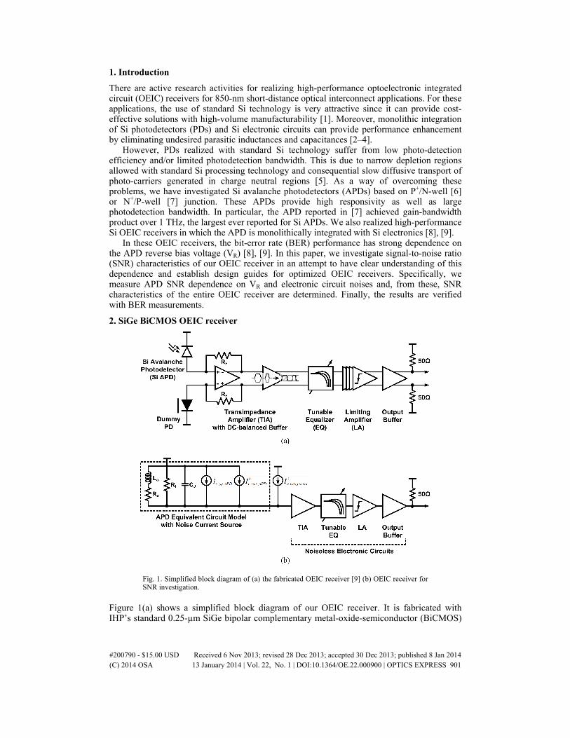
Fig. 1. Simplified block diagram of (a) the fabricated OEIC receiver [9] (b) OEIC receiver for SNR investigation.
Figure 1(a) shows a simplified block diagram of our OEIC receiver. It is fabricated with IHP’s standard 0.25-µm SiGe bipolar complementary metal-oxide-semiconductor (BiCMOS)
#200790 - $15.00 USD Received 6 Nov 2013; revised 28 Dec 2013; accepted 30 Dec 2013; published 8 Jan 2014(C) 2014 OSA 13 January 2014 | Vol. 22, No. 1 | DOI:10.1364/OE.22.000900 | OPTICS EXPRESS 901

technology [10], and composed of a Si APD along with a dummy PD, a transimpedance amplifier (TIA) with DC-balanced buffer, a tunable equalizer, a limiting amplifier, and an output buffer. The APD is realized P+/N-well junction surrounded by shallow trench isolation. The optical window is about 10 µm × 10 µm. The dummy PD provides TIA input symmetry. The TIA is designed in shunt-feedback configuration to achieve low-noise characteristics, and a DC-balanced buffer is used for fully differential signaling. The equalizer compensates bandwidth limitation of APD and TIA, and its high-frequency boosting gain can be tuned with a capacitor array. The limiting amplifier is composed of four-stage differential amplifier having emitter degeneration, and the output buffer is used for driving 50-Ω loads. The power consumption excluding the output buffer is about 59 mW with 2.5-V supply voltage. It can achieve 12.5-Gb/s operation with BER of 10−12. Further details for this OEIC receiver can be found in [9].
3. Signal-to-noise ratio (SNR) determination
Figure 1(b) illustrates a simplified block diagram of our OEIC receiver used for SNR investigation. An APD equivalent circuit model [11] including a noise current source is shown, and the electronic circuit noise is modeled with an input-referred noise current source. Then, SNRs for APD (SNRAPD) and OEIC receiver (SNROEIC) can be described as:
, , RAPD R
2, , R
(V )SNR (V ) ,
(V )
s pp APD
n rms APD
I
I= (1)
, , ROEIC R
2 2, , R , ,
(V )SNR (V ) ,
(V )
s pp APD
n rms APD n rms circuit
I
I I=
+ (2)
where Is,pp,APD and In,rms,APD represent peak-to-peak signal current and root mean square (rms) noise current of APD, respectively, both of which depend on VR. In,rms,circuit represents rms input-referred noise current of the electronic circuits. By measuring Is,pp,APD, In,rms,APD, and In,rms,circuit at different VR values, numerical values for SNRAPD and SNROEIC can be determined.
3.1 Si avalanche photodetector (APD)
Fig. 2. Experimental setups for APD signal and noise measurement.
For measuring Is,pp,APD and In,rms,APD, the setup shown in Fig. 2 is used. For signal measurement, 850-nm light from a laser diode is modulated at 1 GHz by an external electro-
#200790 - $15.00 USD Received 6 Nov 2013; revised 28 Dec 2013; accepted 30 Dec 2013; published 8 Jan 2014(C) 2014 OSA 13 January 2014 | Vol. 22, No. 1 | DOI:10.1364/OE.22.000900 | OPTICS EXPRESS 902

optic modulator. 1-GHz modulation is used because it is experimentally found that APD photodetection frequency response is very flat around this frequency resulting in more reliable experimental results. The modulated light is transmitted through multimode fiber, and injected into the APD through a lensed fiber. The signal power is determined by measuring APD output signal at 1 GHz with a spectrum analyzer having 50-Ω load.
The noise power spectral density at 1 GHz is measured using the spectrum analyzer with unmodulated optical input as shown in Fig. 2. Since the resulting noise level is less than the resolution limit of our spectrum analyzer, APD output signal is amplified with a commercial low-noise amplifier (LNA) having 26-dB gain and 3-dB noise figure. APD noise power spectral density is determined by calibrating these results with LNA gain and noise figure. Since APD noises are dominated by thermal and shot noises, which are white noises [12], the total APD noise power can be obtained by multiplying the measured noise power spectral density at 1 GHz with the equivalent noise bandwidth determined from the measured photodetection frequency response of our APD [9]. Then, the measured APD signal and noise power are converted into Is,pp,APD and In,rms,APD, respectively. For this, the influence of APD output impedance can be ignored since it is much larger than 50-Ω load provided by the spectrum analyzer.
Fig. 3. Measured APD (a) signal and (b) noise characteristics as a function of reverse bias voltage (VR).
Figure 3 shows measured Is,pp,APD and In,rms,APD as a function of VR at two different incident optical powers (Popt) of –8 and –10 dBm. With increasing VR, Is,pp,APD increases due to avalanche gain, reaching the maximum at VR of about 12.4 V. As expected, Is,pp,APD is larger
#200790 - $15.00 USD Received 6 Nov 2013; revised 28 Dec 2013; accepted 30 Dec 2013; published 8 Jan 2014(C) 2014 OSA 13 January 2014 | Vol. 22, No. 1 | DOI:10.1364/OE.22.000900 | OPTICS EXPRESS 903

for larger Popt. The maximum responsivity of our APD is about 1.4 A/W, which is much lower compared to conventional 850-nm APDs. This is due to the fact that our APD is realized with the standard Si technology which does not allow optimal APD device structure. In,rms,APD also increases with increasing VR due to increasing avalanche noise. In,rms,APD is slightly larger for larger Popt as shown in the inset of Fig. 3(b). Both noise currents are nearly the same for VR below about 11.5 V since the thermal noise is the dominant noise for APD in the range. With increasing VR, the shot noise becomes more pronounced, and consequently, larger Popt produces larger In,rms,APD [13].
3.2 Electronic circuits
For measuring In,rms,circuit, a receiver IC without on-chip APD fabricated within the same run as our OEIC receiver is used. For noise measurement, the input node is left open, and one of two differential outputs is terminated with 50-Ω load, and the other is connected to a spectrum analyzer [14]. Equalizer boosting gain is set at it minimum value of 4 dB to minimize the effects of noise boosting. The noise frequency characteristics are measured from 100 MHz to 10 GHz, and the effect of electrical cable loss is compensated. Although noise characteristics can be affected by RF pads used for the measurement purpose, their influence is not significant since the pad capacitance is relatively small. The output noise power is converted into output noise voltage, and then, the output noise voltage is referred to the input node by dividing the resulting output noise voltage with the measured transimpedance frequency response of the receiver IC.
Fig. 4. Measured and simulated signal and noise frequency characteristics of electronic circuits with minimum equalization.
Figure 4 shows the resulting input-referred noise current density (in,circuit) as well as the measured transimpedance frequency response of the receiver IC. In,rms,circuit can be determined using below equation [15]:
2 2, , ,100
,BWs
nn rms circuit n circuitMHz
s
BWI i df
BW = ⋅ (3)
where BWs and BWn is the signal and equivalent noise bandwidth of the receiver IC, respectively. The resulting In,rms,circuit of our electronic circuits is about 0.83 µArms. Figure 4 also shows our measurement results agree well with the simulation results. For both transimpedance and noise simulation, Spectre simulator in Cadence is used.
#200790 - $15.00 USD Received 6 Nov 2013; revised 28 Dec 2013; accepted 30 Dec 2013; published 8 Jan 2014(C) 2014 OSA 13 January 2014 | Vol. 22, No. 1 | DOI:10.1364/OE.22.000900 | OPTICS EXPRESS 904

3.3 OEIC receiver
Fig. 5. Measured APD signal and noise current with and without electronic circuit noise at incident optical power (Popt) of (a) –8 and (b) –10 dBm, respectively.
Figure 5 shows APD signal current along with two different noise currents, one for APD alone and the other for the total OEIC receiver, at different bias voltages with two different Popt levels of –8 and –10 dBm. It can be observed that the total OEIC receiver noise is dominated by the APD noise when VR approaches the breakdown voltage.
Fig. 6. Estimated SNRAPD and SNROEIC as a function of VR at incident optical power (Popt) of –8 and –10 dBm, respectively.
With these measurement results, numerical values for SNRAPD and SNROEIC can be determined using Eq. (1) and Eq. (2). Figure 6 shows the resulting SNRAPD and SNROEIC at different bias voltages. SNRAPD is the highest for VR of about 11.9 V, which is less than VR of 12.4 V that gives the maximum APD signal current shown in Fig. 3(a). For VR below 11.9 V, SNRAPD is degraded because APD does not have sufficient avalanche gain. For VR above 11.9 V, there is too much APD noise. The short-dashed lines in Fig. 6 show the estimated
#200790 - $15.00 USD Received 6 Nov 2013; revised 28 Dec 2013; accepted 30 Dec 2013; published 8 Jan 2014(C) 2014 OSA 13 January 2014 | Vol. 22, No. 1 | DOI:10.1364/OE.22.000900 | OPTICS EXPRESS 905

SNROEIC. It has the highest value for VR of about 12.0 V. The optimal VR for SNROEIC is slightly higher than that for SNRAPD since APD needs to provide slightly larger gain due to the circuit noise.
4. Confirmation by bit-error rate measurement
Fig. 7. Measured and estimated BER as a function of VR at incident optical power (Popt) of –8 and –10 dBm, respectively.
To verify the accuracy of the estimated SNROEIC, BER performance of our OEIC receiver is measured at different reverse bias voltages, and the results are compared with the BER determined from SNROEIC. For this measurement, equalizer boosting gain is minimized to alleviate any noise boosting and signal distortion due to over-equalized frequency response. In addition, the data rate is set below the OEIC receiver 3-dB bandwidth of 7.5 GHz [9] to avoid any BER degradation due to inter-symbol interference caused by limited OEIC receiver bandwidth. Figure 7 shows the measured BER when 6-Gb/s broadband optical data are detected by our OEIC receiver at Popt of –8 and –10 dBm, respectively. The short-dashed lines in Fig. 7 show the estimated BER derived with the following equation:
OEICSNR1BER .
2 2 2erfc
α ⋅ = ⋅
(4)
In Eq. (4), α represents signal penalties due to fiber dispersion, transmitter bandwidth, and experimental loss [16]. In our case, α is estimated to be 0.88 by fitting measured data to Eq. (4) with the minimum squared error. As shown in Fig. 7, for Popt of –10 dBm, the best BER performance is achieved at VR of about 12.0 V, corresponding to VR having the highest SNROEIC as shown in Fig. 6. For Popt of –8 dBm, the measured BER is equal to or less than 10−12 for VR of from 11.6 V to 12.2 V. Although not shown in Fig. 7, the fitting curve has the minimum BER of about 10−19 at VR of about 12.0 V, which corresponds to the VR having the highest SNROEIC for Popt of –8 dBm.
5. Conclusion
We investigate SNR characteristics of an OEIC receiver fabricated with standard 0.25-µm SiGe BiCMOS technology. APD signal and noise characteristics are determined at different VR values, and electronic circuit noise is measured. With measurement results, SNR
#200790 - $15.00 USD Received 6 Nov 2013; revised 28 Dec 2013; accepted 30 Dec 2013; published 8 Jan 2014(C) 2014 OSA 13 January 2014 | Vol. 22, No. 1 | DOI:10.1364/OE.22.000900 | OPTICS EXPRESS 906

characteristics of our OEIC receiver are determined, and the results are verified with BER measurement.
Acknowledgments
This work was supported by the National Research Foundation of Korea (NRF) grant funded by the Korea government (MEST) [2012R1A2A1A01009233]. The authors would like to thank Minsu Ko and Jeong-Min Lee in High-Speed Circuits and Systems Laboratory, Yonsei University, for many helpful discussions. The authors are also very thankful to IC Design Education Center (IDEC) for EDA software support.
#200790 - $15.00 USD Received 6 Nov 2013; revised 28 Dec 2013; accepted 30 Dec 2013; published 8 Jan 2014(C) 2014 OSA 13 January 2014 | Vol. 22, No. 1 | DOI:10.1364/OE.22.000900 | OPTICS EXPRESS 907