‘soft electronic matter’, …ufdcimages.uflib.ufl.edu/uf/e0/04/32/36/00001/mickel_p.pdf‘soft...
TRANSCRIPT
‘SOFT ELECTRONIC MATTER’, MAGNETOELECTRIC COUPLING, ANDMULTIFERROISM IN COMPLEX OXIDES
By
PATRICK R. MICKEL
A DISSERTATION PRESENTED TO THE GRADUATE SCHOOLOF THE UNIVERSITY OF FLORIDA IN PARTIAL FULFILLMENT
OF THE REQUIREMENTS FOR THE DEGREE OFDOCTOR OF PHILOSOPHY
UNIVERSITY OF FLORIDA
2011
c© 2011 Patrick R. Mickel
2

To my father
3

ACKNOWLEDGMENTS
A Ph.D. is a long road that requires committed support from numerous people, both
professionally and personally. As the saying goes, it takes a village to raise a graduate
student - and my case is no exception. It is impossible to thank everyone who has
hepled me along the way, but below are my attempts.
First and foremost, I am forever grateful for the opportunities that Art has provided
me. I came to him lost in the world of bio-physics, and he gave me the guidance and
support I needed, helping me turn my graduate career 180 around. The stimulating
projects, and positive environment that surround him have truly changed my life. Art
provided invaluable feedback and insight into every problem I presented him, and I will
forever aspire to understand physics as simply and deeply as he does.
My committee members have all helped me reach this point successfully. Amlan,
my unofficial second advisor, has provided me indispensable support. Our daily
conversations, which often end in laughter, are a cornerstone in my graduate education.
Without him, none of this work would be possible. Dr. Rinzler has also helped shape my
graduate career, and I am very grateful for his support during my lab transition. As my
teacher, Dr. Hershfield has greatly improved my understanding of quantum mechanics.
His door has always been open for questions concerning both class and research. I am
also very grateful for all the ways I have learned with Dr. Dempere. Through her class
on SEM, and the opportunities she provided me working at MAIC, I learned valuable
characterization techniques and concepts that still help me today.
I have also benefited greatly from many discussions and relationships with other
members of the University of Flordia Physics Department. First, my collaboration
with Dr. Pradeep Kumar was quite fruitful, as he taught me a great deal about
magnetoelectric coupling. The theoretical understanding of magnetoelectric coupling
in this thesis would not have been possible without him. The time I spent in Dr. Tom
Mareci’s lab was also valuable, as I learned the inner workings of Diffusion Tensor
4

Imaging. Also, many students have augmented my education along the way and I list
them here in no particular order: Hyoungjeen Jeen, Sinan Selcuk, Sefaatin Tongay,
Pooja Wadhwa, Evan Donoghue, Manoj Srivastava, Andrei Kamalov, Ritesh Das,
Gueenta Singh-Bhalla, Siddhartha Ghosh, Greg Boyd, Rajiv Misra, Maureen Petterson,
Sanal Buvaev, Dan Pajerowski, Chris Pankow, Mitch McCarthy, Corey Stambaugh, and
Patrick Hearin.
I would also like to acknowledge the staffs of machine shop and electric shop.
In particular the cryogenic staffs, Greg and John, provided our labs an incredible
advantage in research through their constant supply of liquid He and N2 all year around
24/7. Also, thanks to Jay Hornton (a really nice guy) for looking after all the pumps and
chillers. Without the help of these hard workers, my work would have taken exponentially
longer to complete.
Prior to my time at the University of Florida, many people were instrumental
in nurturing my scientific career. Dr. Daniel Fleisch, my first mentor, was incredibly
generous with his time as he introduced me to science and research. My undergraduate
professors at the University of Notre Dame also provided an important chapter in my
education. Their doors were always open, even outside of office hours, as they instilled
confidence and knowledge in me. Dr. Kathy Newman, Dr. Zoltan Neda, and Dr. Mitchell
Wayne were particularly generous and patient.
Last but certainly not least, I would like to thank my family and future wife Kristina.
They support me in everything I do, and have made me who I am. Without them I am
nothing.
5

TABLE OF CONTENTS
page
ACKNOWLEDGMENTS . . . . . . . . . . . . . . . . . . . . . . . . . . . . . . . . . . 4
LIST OF FIGURES . . . . . . . . . . . . . . . . . . . . . . . . . . . . . . . . . . . . . 9
ABSTRACT . . . . . . . . . . . . . . . . . . . . . . . . . . . . . . . . . . . . . . . . . 12
CHAPTER
1 Basic Physics Review . . . . . . . . . . . . . . . . . . . . . . . . . . . . . . . . 14
1.1 Mixed Valence Manganites . . . . . . . . . . . . . . . . . . . . . . . . . . 141.1.1 Introduction . . . . . . . . . . . . . . . . . . . . . . . . . . . . . . . 141.1.2 Structure and Energy Diagrams . . . . . . . . . . . . . . . . . . . . 151.1.3 Effects of Doping and Cation Substitution . . . . . . . . . . . . . . 181.1.4 La1−xCaxMnO3, Pr1−xCaxMnO3, and (La1−yPry )1−xCaxMnO3 . . . 21
1.2 Multiferroics . . . . . . . . . . . . . . . . . . . . . . . . . . . . . . . . . . . 281.2.1 Introduction . . . . . . . . . . . . . . . . . . . . . . . . . . . . . . . 281.2.2 Ferromagnetism . . . . . . . . . . . . . . . . . . . . . . . . . . . . 291.2.3 Ferroelectricity . . . . . . . . . . . . . . . . . . . . . . . . . . . . . 341.2.4 Magnetoelectric Multiferroics . . . . . . . . . . . . . . . . . . . . . 43
1.3 Magnetoelectric Coupling . . . . . . . . . . . . . . . . . . . . . . . . . . . 481.3.1 Introduction . . . . . . . . . . . . . . . . . . . . . . . . . . . . . . . 481.3.2 Maxwell Equations vs. Magnetoelectric Coupling . . . . . . . . . . 501.3.3 Free Energy . . . . . . . . . . . . . . . . . . . . . . . . . . . . . . . 52
2 Experimental Techniques . . . . . . . . . . . . . . . . . . . . . . . . . . . . . . 54
2.1 Sample Fabrication . . . . . . . . . . . . . . . . . . . . . . . . . . . . . . . 542.1.1 Growth Methods . . . . . . . . . . . . . . . . . . . . . . . . . . . . 542.1.2 Structural and Compositional Characterizations . . . . . . . . . . . 55
2.2 Temperature and Magnetic Field Control . . . . . . . . . . . . . . . . . . . 562.3 Resistance . . . . . . . . . . . . . . . . . . . . . . . . . . . . . . . . . . . 572.4 Capacitance Measurements . . . . . . . . . . . . . . . . . . . . . . . . . . 58
2.4.1 Capacitance Bridge and Stick . . . . . . . . . . . . . . . . . . . . . 582.4.2 Dielectric Electrodes . . . . . . . . . . . . . . . . . . . . . . . . . . 602.4.3 Interdigital Capacitance . . . . . . . . . . . . . . . . . . . . . . . . 632.4.4 Bandwidth Temperature Sweeps . . . . . . . . . . . . . . . . . . . 65
2.5 Ferroelectric Measurements . . . . . . . . . . . . . . . . . . . . . . . . . . 672.5.1 Sawyer-Tower Circuit . . . . . . . . . . . . . . . . . . . . . . . . . . 672.5.2 Precision LC: Ferroelectric Tester . . . . . . . . . . . . . . . . . . . 692.5.3 Remanent Polarization . . . . . . . . . . . . . . . . . . . . . . . . . 70
6
3 ‘Soft Electronic Matter’ in LPCMO . . . . . . . . . . . . . . . . . . . . . . . . . 73
3.1 Introduction . . . . . . . . . . . . . . . . . . . . . . . . . . . . . . . . . . . 733.2 Transport Properties . . . . . . . . . . . . . . . . . . . . . . . . . . . . . . 74
3.2.1 Resistance . . . . . . . . . . . . . . . . . . . . . . . . . . . . . . . 743.2.2 Complex Capacitance . . . . . . . . . . . . . . . . . . . . . . . . . 74
3.3 Competing Dielectric Phases . . . . . . . . . . . . . . . . . . . . . . . . . 793.3.1 Modeling . . . . . . . . . . . . . . . . . . . . . . . . . . . . . . . . . 803.3.2 Temperature Dependence of Model Parameters . . . . . . . . . . . 81
3.4 ‘Soft Electronic Matter’ . . . . . . . . . . . . . . . . . . . . . . . . . . . . . 853.4.1 Polarons and Detailed Balance . . . . . . . . . . . . . . . . . . . . 853.4.2 Testing Detailed Balance Constraints . . . . . . . . . . . . . . . . . 873.4.3 Lattice Relaxation Rates . . . . . . . . . . . . . . . . . . . . . . . . 903.4.4 Charge Density Waves . . . . . . . . . . . . . . . . . . . . . . . . . 91
3.5 Summary . . . . . . . . . . . . . . . . . . . . . . . . . . . . . . . . . . . . 93
4 Strain Mediated Magnetoelectric Coupling in (La1−yPry )1−xCaxMnO3 . . . . . 95
4.1 Introduction . . . . . . . . . . . . . . . . . . . . . . . . . . . . . . . . . . . 954.2 Dielectric Constant Tuning . . . . . . . . . . . . . . . . . . . . . . . . . . . 96
4.2.1 Experimental Results . . . . . . . . . . . . . . . . . . . . . . . . . . 964.2.2 Modeling . . . . . . . . . . . . . . . . . . . . . . . . . . . . . . . . . 97
4.3 Activation Energy Tuning . . . . . . . . . . . . . . . . . . . . . . . . . . . 994.3.1 Experimental Results . . . . . . . . . . . . . . . . . . . . . . . . . . 994.3.2 Comparison of Magnetoelectric Couplings . . . . . . . . . . . . . . 101
4.4 Film Thickness Study . . . . . . . . . . . . . . . . . . . . . . . . . . . . . 1014.5 Summary . . . . . . . . . . . . . . . . . . . . . . . . . . . . . . . . . . . . 103
5 Multiferroism in BiMnO3 . . . . . . . . . . . . . . . . . . . . . . . . . . . . . . . 105
5.1 Introduction . . . . . . . . . . . . . . . . . . . . . . . . . . . . . . . . . . . 1055.2 Characterizations . . . . . . . . . . . . . . . . . . . . . . . . . . . . . . . . 105
5.2.1 Structural Characterization . . . . . . . . . . . . . . . . . . . . . . . 1065.2.2 Magnetic Characterization . . . . . . . . . . . . . . . . . . . . . . . 1075.2.3 Resistive Characterization . . . . . . . . . . . . . . . . . . . . . . . 1095.2.4 Ferroelectric Characterization . . . . . . . . . . . . . . . . . . . . . 1095.2.5 Dielectric Characterization . . . . . . . . . . . . . . . . . . . . . . . 112
5.3 Nature of Ferroelectricity . . . . . . . . . . . . . . . . . . . . . . . . . . . . 1155.3.1 Relaxor Review . . . . . . . . . . . . . . . . . . . . . . . . . . . . . 1155.3.2 Comparison . . . . . . . . . . . . . . . . . . . . . . . . . . . . . . . 1165.3.3 Pulse Sequencing . . . . . . . . . . . . . . . . . . . . . . . . . . . 1185.3.4 Island Growth . . . . . . . . . . . . . . . . . . . . . . . . . . . . . . 119
5.4 Summary . . . . . . . . . . . . . . . . . . . . . . . . . . . . . . . . . . . . 121
7

6 Tuning Ferroelectricity in BiMnO3 . . . . . . . . . . . . . . . . . . . . . . . . . . 122
6.1 Introduction . . . . . . . . . . . . . . . . . . . . . . . . . . . . . . . . . . . 1226.2 Strain: External and Island Edges . . . . . . . . . . . . . . . . . . . . . . 123
6.2.1 External Strain . . . . . . . . . . . . . . . . . . . . . . . . . . . . . 1236.2.2 Electrode “Lensing” . . . . . . . . . . . . . . . . . . . . . . . . . . . 1256.2.3 Island Edge Strain Gradients . . . . . . . . . . . . . . . . . . . . . 125
6.3 Magnetoelectric Coupling in BiMnO3 . . . . . . . . . . . . . . . . . . . . . 1266.3.1 Remanent Polarization Tuning . . . . . . . . . . . . . . . . . . . . . 1266.3.2 Reorientation Time-Scales . . . . . . . . . . . . . . . . . . . . . . . 1276.3.3 Connection to Lattice Transition . . . . . . . . . . . . . . . . . . . . 128
6.4 Summary . . . . . . . . . . . . . . . . . . . . . . . . . . . . . . . . . . . . 130
REFERENCES . . . . . . . . . . . . . . . . . . . . . . . . . . . . . . . . . . . . . . . 131
BIOGRAPHICAL SKETCH . . . . . . . . . . . . . . . . . . . . . . . . . . . . . . . . 137
8
LIST OF FIGURES
Figure page
1-1 Cubic ABO3 Perovskite Manganite Structure . . . . . . . . . . . . . . . . . . . 16
1-2 Orbital Energy Levels: Crystal Field Splitting and Jahn-Teller Distortions . . . . 16
1-3 Cubic and Jahn-Teller Distrotion of MnO6 Octahedra . . . . . . . . . . . . . . . 18
1-4 3d Orbitals: eg and t2g . . . . . . . . . . . . . . . . . . . . . . . . . . . . . . . . 19
1-5 Polaron Depiction . . . . . . . . . . . . . . . . . . . . . . . . . . . . . . . . . . 19
1-6 La1−xCaxMnO3 Phase Diagram . . . . . . . . . . . . . . . . . . . . . . . . . . . 22
1-7 Pr1−xCaxMnO3 Phase Diagram . . . . . . . . . . . . . . . . . . . . . . . . . . . 23
1-8 (La1−yPry )1−xCaxMnO3 Phase Diagram . . . . . . . . . . . . . . . . . . . . . . 25
1-9 Dark-Field Electron Diffraction Image of Phase Separation . . . . . . . . . . . 26
1-10 Magnetic Force Microscopy . . . . . . . . . . . . . . . . . . . . . . . . . . . . . 27
1-11 Multiferroic Coupling Schematic . . . . . . . . . . . . . . . . . . . . . . . . . . . 30
1-12 Types of Magnetic Ordering . . . . . . . . . . . . . . . . . . . . . . . . . . . . . 31
1-13 M-H Loops for Different Magnetic Orderings . . . . . . . . . . . . . . . . . . . . 32
1-14 Stoner Band Theory of Ferromagnetism . . . . . . . . . . . . . . . . . . . . . . 35
1-15 Polarization vs. Electric Field Loops for Different Electric Orderings . . . . . . . 36
1-16 Ferroelectric Bananas . . . . . . . . . . . . . . . . . . . . . . . . . . . . . . . . 37
1-17 Ferroelectric Unit Cell . . . . . . . . . . . . . . . . . . . . . . . . . . . . . . . . 39
1-18 Ferroelectric Energy Diagrams . . . . . . . . . . . . . . . . . . . . . . . . . . . 40
1-19 Antisymmetric Dzyaloshinskii-Moriya Interaction . . . . . . . . . . . . . . . . . 42
1-20 Composite Multiferroic Geometries . . . . . . . . . . . . . . . . . . . . . . . . . 45
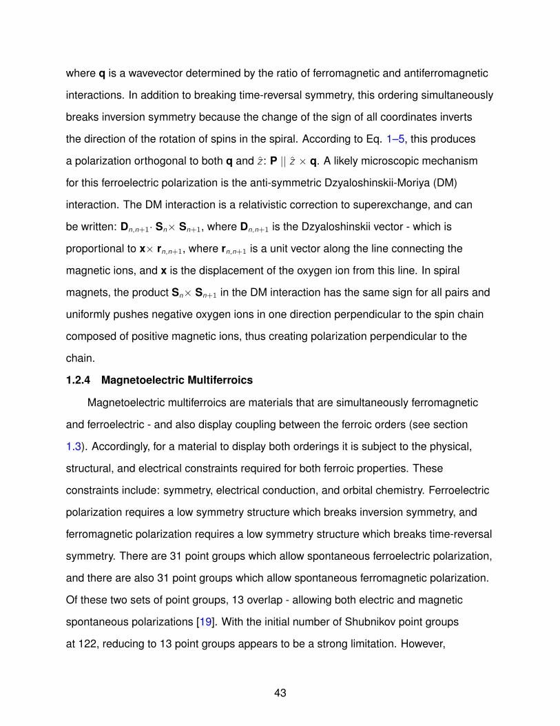
1-21 Bi 6s Lone Pair . . . . . . . . . . . . . . . . . . . . . . . . . . . . . . . . . . . . 47
1-22 Magnetoelectric Revival . . . . . . . . . . . . . . . . . . . . . . . . . . . . . . . 49
1-23 Magnetoelectric Multiferroic Venn Diagram . . . . . . . . . . . . . . . . . . . . 50
2-1 PLD Schematic and Image . . . . . . . . . . . . . . . . . . . . . . . . . . . . . 55
2-2 PPMS Sample Chamber Schematic . . . . . . . . . . . . . . . . . . . . . . . . 57
9

2-3 Four-Terminal Resistance Geometry . . . . . . . . . . . . . . . . . . . . . . . . 58
2-4 HP4284 Circuitry . . . . . . . . . . . . . . . . . . . . . . . . . . . . . . . . . . . 59
2-5 Dielectric Electrode Circuits . . . . . . . . . . . . . . . . . . . . . . . . . . . . . 61
2-6 Maxwell-Wagner Circuit Simulation . . . . . . . . . . . . . . . . . . . . . . . . . 63
2-7 Interdigital Capacitance Fundamentals . . . . . . . . . . . . . . . . . . . . . . . 64
2-8 Interdigital Capacitance Fabrication . . . . . . . . . . . . . . . . . . . . . . . . 65
2-9 Multi-Frequency Consistency Check . . . . . . . . . . . . . . . . . . . . . . . . 67
2-10 Sawyer-Tower Circuit . . . . . . . . . . . . . . . . . . . . . . . . . . . . . . . . 68
2-11 Precision LC Circuitry . . . . . . . . . . . . . . . . . . . . . . . . . . . . . . . . 70
2-12 Remanent Polarization Pulse Sequence . . . . . . . . . . . . . . . . . . . . . . 72
3-1 DC Resistance vs. Temperature . . . . . . . . . . . . . . . . . . . . . . . . . . 75
3-2 Complex Capacitance vs. Frequency . . . . . . . . . . . . . . . . . . . . . . . . 76
3-3 Cole-Cole Plot . . . . . . . . . . . . . . . . . . . . . . . . . . . . . . . . . . . . 77
3-4 Logarithmic Parametric Slope . . . . . . . . . . . . . . . . . . . . . . . . . . . . 78
3-5 Competing Dielectric Phase Ansatz . . . . . . . . . . . . . . . . . . . . . . . . 79
3-6 Circuit Model . . . . . . . . . . . . . . . . . . . . . . . . . . . . . . . . . . . . . 81
3-7 Model Results . . . . . . . . . . . . . . . . . . . . . . . . . . . . . . . . . . . . 82
3-8 β vs. Temperature . . . . . . . . . . . . . . . . . . . . . . . . . . . . . . . . . . 83
3-9 ramp vs. Temperature . . . . . . . . . . . . . . . . . . . . . . . . . . . . . . . . . 84
3-10 Arrheniuis Plot of Relaxation Time-Scales . . . . . . . . . . . . . . . . . . . . . 84
3-11 Polaron Depiction . . . . . . . . . . . . . . . . . . . . . . . . . . . . . . . . . . 85
3-12 Detailed Balance 3 State Model . . . . . . . . . . . . . . . . . . . . . . . . . . . 86
3-13 ramp vs. Temperature . . . . . . . . . . . . . . . . . . . . . . . . . . . . . . . . . 88
3-14 Energy/Population Schematic . . . . . . . . . . . . . . . . . . . . . . . . . . . . 89
3-15 Thickness Dependence of Dielectric Constatns . . . . . . . . . . . . . . . . . . 91
3-16 Energy/Population Schematic . . . . . . . . . . . . . . . . . . . . . . . . . . . . 92
3-17 Charge Density Wave Schematic . . . . . . . . . . . . . . . . . . . . . . . . . . 93
10

4-1 Magnetic Tuning of Dielectric Constants . . . . . . . . . . . . . . . . . . . . . . 97
4-2 Magnetic Tuning of Activation Energies . . . . . . . . . . . . . . . . . . . . . . 100
4-3 Modeling Results for Multiple Thickness Films . . . . . . . . . . . . . . . . . . . 102
4-4 Strain Dependence of Magnetoelectric Coupling . . . . . . . . . . . . . . . . . 103
5-1 Monoclinic Unit Cell of BiMnO3 . . . . . . . . . . . . . . . . . . . . . . . . . . . 106
5-2 BiMnO3 Θ− 2Θ Scans . . . . . . . . . . . . . . . . . . . . . . . . . . . . . . . 108
5-3 Magnetic Characterization . . . . . . . . . . . . . . . . . . . . . . . . . . . . . . 110
5-4 Remanent Hysteresis Loops . . . . . . . . . . . . . . . . . . . . . . . . . . . . 111
5-5 Frequency Dependence of Imaginary Capacitance . . . . . . . . . . . . . . . . 113
5-6 Arrhenius Plot of Relaxtion Time-Scales . . . . . . . . . . . . . . . . . . . . . . 114
5-7 Temperature Dependence of Real Capacitance . . . . . . . . . . . . . . . . . . 115
5-8 Dielectric Prediction of Ferroelectric TC . . . . . . . . . . . . . . . . . . . . . . 118
5-9 Dual Pulse Sequence Results . . . . . . . . . . . . . . . . . . . . . . . . . . . . 120
6-1 External Strain Geometry . . . . . . . . . . . . . . . . . . . . . . . . . . . . . . 124
6-2 Strain Tuning of Ferroelectricity . . . . . . . . . . . . . . . . . . . . . . . . . . . 124
6-3 Electrode “Lensing” . . . . . . . . . . . . . . . . . . . . . . . . . . . . . . . . . 126
6-4 Island Strain . . . . . . . . . . . . . . . . . . . . . . . . . . . . . . . . . . . . . 127
6-5 Magnetoelectric Coupling in BiMnO3 . . . . . . . . . . . . . . . . . . . . . . . . 128
6-6 Pulse Sequence in Magnetic Fields . . . . . . . . . . . . . . . . . . . . . . . . 129
6-7 Correlation of Couplings . . . . . . . . . . . . . . . . . . . . . . . . . . . . . . . 129
11

Abstract of Dissertation Presented to the Graduate Schoolof the University of Florida in Partial Fulfillment of theRequirements for the Degree of Doctor of Philosophy
‘SOFT ELECTRONIC MATTER’, MAGNETOELECTRIC COUPLING, ANDMULTIFERROISM IN COMPLEX OXIDES
By
Patrick R. Mickel
August 2011
Chair: Arthur F. HebardMajor: Physics
This thesis has focused on the electronic and magnetic properties of thin-film
oxide crystals. Oxides are home to some of the richest physics in condensed matter,
producing complex features in response to changes in temperature, electric/magnetic
fields, and strain. Three of these features have gained particular prominence, and
are among the most active research topics today: phase separation, magnetoelectric
coupling, and multiferroism.
“Phase separation” describes the state of materials containing neighboring regions
with distinct electronic and magnetic properties - an important phenomenon associated
with some of the most exotic material properties known: colossal magnetoresistance,
multiferriosm, and high-temperature superconductivity. Phase separation is commonly
explained by disorder and strain, resulting in static and stationary phases. However,
It is shown here that competing dielectric phases dynamically transform into one
another over macroscopic lengths and long time periods (10−3 − 10−5 seconds, and 1
µm2), indicating the phases are far from static. These results argue for a fundamental
reinterpretation of the physics of phase separation from localized rigid structures to
wave-like thermodynamic entities.
Magnetoelectric coupling describes the induction of electric (magnetic) polarization
via magnetic (electric) fields, and has myriad applications from sensors to data storage.
Lattice strain is commonly proposed as a mediating mechanism, but these conjectures
12

have remained primarily phenomenological. However, this thesis introduces a first
principles strain-based microscopic model that describes the measured magnetoelectric
coupling of competing dielectric phases. The results of this model accurately reproduce
the effects of magnetic fields on the capacitive properties of both dielectric phases,
as well as predict additional results seen in the literature. These results provides a
direct experimental check of strain’s role in magnetoelectric coupling of single phases,
and marks an important step forward in understanding the mechanisms producing
magnetoelectric coupling.
Multiferroics are materials that display two separate orderings, typically spontaneous
magnetization (ferromagnetism) and electric polarization (ferroelectricity). These
materials promise technological revolutions and are arguably the most intensely
researched subject in materials science today. This thesis describes the single-phase
multiferroic, BiMnO3, providing important evidence for the growing debate concerning its
ferroelectric nature. It is shown that BiMnO3 displays relaxor ferroelectricity, and that its
remanent polarization is highly tunable, decreasing by as much as 10% in 7 T magnetic
fields, and increasing by almost 50% under small externally induced strains.
13

CHAPTER 1BASIC PHYSICS REVIEW
1.1 Mixed Valence Manganites
1.1.1 Introduction
The basic electric and thermal properties of manganites were first investigated
as early as the 1950’s [1], where a large magnetoresistance was discovered near
the ferromagnetic Curie temperature, TC , producing moderate interest in the physics
community. In 1994, however, research in manganites surged in response to a
new-found phenomena: colossal magnetoresistance, where magnetic fields were
found to induce a decrease in resistance by more than a factor of 103 [2]. The initial
dream was to someday replace the ubiquitous giant-magnetoresistance (GMR) effect,
which had quickly become the standard in the magnetic information storage industry
for read-heads. GMR is based on spin-valve mechanisms and results in a few tens of
percent change in resistance, so colossal magnetoresistance provided a huge potential
for improved device performance.
As research progressed, however, the vision of manganites changed radically from
what seemed a straightforward application in the magnetic-information-storage industry,
to a colossal challenge to condensed-matter physics. Soon after the reemergence of
manganites, it was realized that their initial theoretical description (i.e. double exchange,
see section 1.1.3) was incapable of quantitatively reproducing the new-found colossal
properties, and that these systems were much more complex than originally thought.
Manganites are now thought of as a quintessential complex-oxide system where
the simultaneous interplay of spin, charge, orbital, and lattice degrees of freedom
spawn some of the most complicated and exotic material properties and physics in
condensed-matter today. These properties include: insulator-to-metal transitions,
charge and orbital ordering, ferro and anti-ferromagnetic ordering, charge density
waves, and multiferroism. Additionally, manganites are extrememly sensitive to external
14

perturbations, with temperature, pressure, light, electric and magnetic fields capable of
drastically altering the balance of phases.
1.1.2 Structure and Energy Diagrams
Manganites crystallize in multiple configurations, including the cubic perovskite,
double-perovskite, and hexagonal structures as well as the general Ruddlesden-Popper
series: An+1BnO3n+1. The manganites studied in this thesis, however, are exclusively
“cubic” perovskites with the B site occupied by Mn atoms and the A site occupied
by a variety of ions: La, Ca, and Pr in the mixed valence manganites, and also Bi in
the following multiferroic discussion. Figure 1-1 shows the basic cubic structure of
the manganite unit cell. The A site atoms occupy the corners of the unit cell and act
primarily as charge reservoirs for doping and space fillers for structural integrity. The Mn
atoms occupy the center of MnO6 oxygen octahedra, the network of which is the primary
mediator of electrical conductivity and magnetic structure within the crystal. The A site
atoms indirectly control the electric and magnetic properties by influencing the valence
and bond angles of the Mn atoms (which necessarily affects its magnetic moment).
Specifically, the electronic and magnetic properties of the crystal are controlled by
the 3d electrons of the Mn atom. Therefore, it is useful to consider the energies of these
orbitals. In isolation, the Mn 3d electrons share a five fold degeneracy: the dxy , dyz , dxz ,
dz2, and dx2−y2 orbitals. However, when the Mn atoms are brought near neighboring
ions, the ambient electric fields can alter the energy levels of the electronic orbitals. This
effect is called “crystal field splitting,” [3] and in cubic perovskites it results in splitting the
5 degenerate 3d orbitals into two groups of energy levels: 3 low-energy t2g orbitals and 2
high-energy eg orbitals. Figure 1-2 illustrates this degeneracy splitting. The energy level
splitting can be understood in terms of Coulomb interactions between the O2p electrons
which lie along the x, y, and z axis of the MnO6 octahedra. The Coulomb potential is
largest for orbitals along these axes, raising the energy of the dz2, and dx2−y2 orbitals
(eg), and lowering the energy of the dxy , dyz , and dxz off axis orbitals (t2g).
15

Figure 1-1. In the cubic perovskite manganite structure, the B site Mn atom (red) isencaged in an O octahetron (black). A site atoms (blue) constitute the cubicshell that supports the octahedron structurally. Alternatively, the structuremay be viewed in terms of MnO2 planes that are separated by AO planes,where the A site atoms lie in the same plane as the apical O atoms of eachoctahedron.
Figure 1-2. The 3d orbital energy levels display to modifications: crystal field splittingand Jahn-Teller distortions. On the left are the 5 degenerage 3d electronorbitals for an atom in isolation. When the atom is placed in the presence ofambient electric fields from ions within a crystal structure the degeneracy isbroken (middle section). And when one eg orbital is occupied by a singleelectron, a spontaneous Jahn-Teller deformation lowers the energy of thesytem by ∆EJT by elongating the z-axis of the unit cell and lowering theCoulomb interaction of the dz2 orbital which is aligned with the neighboringO2p orbital. See Figs. 1-4 and 1-3.
16

For certain valence states of the Mn atom, coulomb repulsions also drive a second
splitting of the orbital energy levels. Odd numbered valence states, such as Mn3+, result
in a singly occupied eg orbital, either dz2 or dx2−y2 - both of which are directly aligned
with the neighboring O2p orbitals. In this configuration, the system may lower its energy
by ∆EJT by spontaneously distorting and elongating along the z-axis to decrease the
Coulomb interaction of the dz2 and O2p electrons, thereby decreasing the potential
energy of the orbital (see Figs. 1-2 and 1-3). Because the overall Coloumbic potential
does not increase, the overall volume of the unit cell remains constant, resulting in a
contraction in the x-y plane which increases the Coulomb interaction of the dx2−y2 and
O2p orbital, raising its potential energy. The t2g orbitals are also effected, with the yz
and xz levels now lower than the xy orbitals, again because of the proximity of the O2p
electrons. This spontaneous energy lowering distortion is called a Jahn-Teller distortion
[4], and is depicted in Figs. 1-2 and 1-3. We note here that this energy gain through
spontaneous distortion is not available in Mn4+ systems because all eg orbitals are
empty and so there are no occupied electron states that decrease in energy, since
the total energy of the t2g levels is constant. This type of distortion, that is dependent
on the presence of an electron is called a polaron. A Polaron is a quasi-particle that
encompasses an electron and the induced lattice distortion surrounding it, see Fig. 1-5.
The crystal field and Jahn-Teller energetic adjustments are important because they
have a direct effect on the magnetic and electric transport properties of manganites.
The lowering of the t2g energy levels results in a localized 3/2 spin which can be treated
as a classical core spin that is tied to the lattice, providing a basis for all the magnetic
orderings present. The formation of the Jahn-Teller polaron and lowering of the eg
energy level modifies the electronic conduction by localizing the eg electrons in a “self”
potential well, resulting in a Mott like insulating state - since the conventional band
picture dictates that LaMnO3 (the prototypical Mn3+ manganite) with it’s singly occupied
eg state should be conducting.
17

B)A)
Figure 1-3. A) The oxygen octahedra of the cubic perovskite structure is shown. B) TheJahn-Teller distorsion is shown. The eg orbital is occupied by a singleelectron allowing it to become energetically favorable for the unit cell todistort from a cubic MnO6 octahedra to an octahedra that is elongated alongthe z-axis (Jahn-Teller distorted). This reduces the orbital overlap andresulting Coulomb potential energy between the Mn dz2 and O2p orbitals.See Fig. 1-4 for 3d orbital orientations, and Fig. 1-2 for the orbital energylevel modifications.
1.1.3 Effects of Doping and Cation Substitution
As mentioned above, the A site atoms indirectly control the electronic and magnetic
properties of the crystal by tunning the valence of the Mn atoms. A site atoms bond
ionically to O atoms, donating their electrons, thus obviating the further ionization of
the Mn atoms by the oxygen octahedra. By populating the A site with a combination of
tri- and di-valent atoms, a mixture of Mn3+ and Mn4+ sites can be created, which can
increase the conductivity by allowing the Mn3+ Jahn-Teller polarons to hop to cubic
undistorted/unoccupied Mn4+ cites. While the conductivity does increase, hopping
between Mn3+ and Mn4+ cites is still an insulating mechanism, due to the inherent
energy barrier involved. However, a balance of Mn3+ and Mn4+ sites can also facilitate a
special form of metallic conduction which is particularly important in manganites: double
exchange.
18

t2g:
eg:
Figure 1-4. The 5 3d orbitals are split into two groups: eg(2) and t2g(3). The 2 eg orbitalsare oriented toward the O atoms on the x, y, and z axes, while the 3 t2gorbitals are not. The Jahn-Teller distortion (see Figs. 1-2 and 1-3) causes anelongation of the unit cell along the z-axis and a contraction in the x-y planemoving O2p orbitals further away and closer, respectively. The decreasedoverlap along the z-axis lowers the energy of the dz2, dxz , and dyz orbitals,and raises the energy of the dx2−y2 and dxy orbitals.
Figure 1-5. A polaron is a quasi-particle that is defined by an electron and the “cloud” ofdistortions it induces in the surrounding lattice sites.
19
Double exchange was first proposed by Zener in 1951 [5] and was later reformulated
by Anderson and Hasegawa in 1955 [6], and consists of the simultaneous transfer of
an electron from a Mn3+ site to an O2− site and the transfer of an electron from an
O2− site to a Mn4+ site. In the charge transfer process, the hopping electrons/polarons
are coupled magnetically to the 3/2 core spin of the t2g orbitals through a large Hund
coupling (> 1eV) that energetically requires that the eg electrons have the same spin
orientation as the core spin at the new location. This results in an effective hopping
matrix between the two Mn atoms of the (simplified) form [6]:
ti ,j = t0i ,jcos(θi ,j/2) (1–1)
where θi ,j is the angle between the core spin and the spin of the eg electron (which
should have approximately the same orientation as the core spin at its initial site). This
hopping process also mediates the paramagnetic-ferromagnetic transition, because as
each eg electron/polaron aligns magnetically with the core spin at the new lattice site it
also induces a slight rotation of the core spin so that effectively, as hopping continues
the orientation of the core spins are gradually rotated to align with the core spins of the
neighboring lattice sites. Once the temperature is low enough to limit thermal fluctuation
of the core spins, this process results in the ferromagnetic alignment of all the spins in
the crystal, and induces an almost simultaneous ferromagnetic and insulator-to-metal
transition [7]. An additional consequence of the large Hund coupling is that at low
temperatures half-doped manganites are half metals with near 100% spin polarization of
the conduction electrons, making them prime candidates for spintronic applications [8].
Double exchange provides a basic description of the magnetoresistance observed
in manganites, near TC the induced alignment of core spins by external fields facilitates
hopping thereby increasing the conductivity resulting in the observed negative
magnetoresistance. This description is only qualitative, however, failing to reproduce
20

the magnitude of the effect. To accurately describe manganites, polaronic, Coulombic,
and exchange interactions must all be accounted for [9–11].
In addition to the valence of the A site atoms, their size also has a strong effect on
the electric and magnetic properties of the crystal. Varying the ionic radii of the A site
atoms can induce additional distortions of the MnO6 octahedra by allowing the O-Mn-O
bonds to buckle away from 180o . This effect is commonly quantified using the “tolerance
factor”:
f =< rA > +rO√2(rMn + rO)
(1–2)
where rA, rO , rMn are the ionic radii of the A site atom, O atom, and Mn atom respectively.
As the tolerance factor decreases from 1, the space group and crystal structure can vary
greatly, from cubic to rhombohedral to orthorhombic. Various tolerance factors can also
promote different orbital and charge ordering which in turn support different magnetic
structures: ferromagnetic, and antiferromagnetic (A, C, CE, and G type. See Ref.
[11]). Additionally, buckling the O-Mn-O bond angle encumbers double exchange by
lowering the hopping integral, preventing the alignment of core spins and delaying the
ferromagnetic and insulator-to-metal transitions to lower temperatures or eliminating
them altogether.
1.1.4 La1−xCaxMnO3, Pr1−xCaxMnO3, and (La1−yPry )1−xCaxMnO3
The manganite discussed in this chapter is the mixed valence manganite of the
composition (La1−yPry )1−xCaxMnO3 (LPCMO). LPCMO is a mixture of two parent
compounds, namely La1−xCaxMnO3 (LCMO) and Pr1−xCaxMnO3 (PCMO), each
of which have complex phase diagrams driven by valence and ionic radii changes
produced by cation substitution (discussed in section 1.1.3). LPCMO is composed
of an incommensurate (inhomogeneous) mixture of LCMO and PCMO, therefore to
understand its properties, it is necessary to review each parent compound.
The two limiting compounds in LCMO’s phase diagram (see Fig. 1-6) are the Mn3+
LaMnO3 and the Mn4+ CaMnO3, however, the properties of LCMO are considerably
21

Figure 1-6. The La1−xCaxMnO3 phase diagram shows the effect of Ca doping, whichintroduces Mn4+ into the completely Mn3+ system LaMnO3. Intermediatedopings produce physics not seen in either parent compound (LaMnO3 andCaMnO3):. At intermediate dopings below 50% a ferromagnetic metallicphase is formed at low temperatures, and intermediate dopings above 50%a charge-ordered insulator with a spatial modulation of the chargedistribution on Mn sites is formed (Mn4+ Mn3+ Mn4+ Mn3+... ). Here, CAFstands for canted antiferromagnet, FI for ferromagnetic insulator, and CO forcharge ordered. The CAF and FI could have spatial inhomogeneity with bothferro- and antiferro-magnetic states present. Figure adapted from Ref.[12, 13].
different than a simple interpolation between the properties of the limiting compounds.
LaMnO3 and CaMnO3 are both paramagnetic insulators at high-temperature and
transition to canted-antiferromagnetic insulators at low temperature. The high-temperature
paramagnetic insulating state remains at all compositions, however, at intermediate
mixings LCMO develops entirely new low-temperature electromagnetic phases. As Ca
doping increases to between 5% and 20% the lower-temperature phase transitions
to a ferromagnetic insulator. Then as Ca increases further to between 20% and 50%
the low-temperature phase becomes a ferromagnetic metal, with the development
22

Figure 1-7. The Pr1−xCaxMnO3 phase diagram shows the effects of Ca doping. Cadoping introduces Mn4+ into the completely Mn3+ system PrMnO3, and alsointroduces structural distortions because the ionic radii of Ca is significantlysmaller than Pr. Like La1−xCaxMnO3, Pr1−xCaxMnO3 develops chargeordering at intermediate dopings, but unlike La1−xCaxMnO3, remainsinsulating for all dopings. The PI, PM, and CI denote the paramagneticinsulating, paramagnetic metallic, and canted insulating states, respectively.The FI and FM denote the ferromagnetic insulating and ferromagneticmetallic states, respectively. TC and TN denote the ferromagnetic Curie andantiferromagnetic Neel temperatures, respectively. Figure reproduced fromRef. [14]
of an insulator-to-metal transition mediated by double exchange. Above 50% Ca
doping results in a low-temperature antiferromagnetic charge-ordered insulating phase
where there is a spatial modulation of the Mn charge distribution (Mn4+ Mn3+ Mn4+
Mn3+...). Above 7/8ths Ca doping the system transitions back to the original canted
antiferromagnetic phase. It should be noted that Ca and La have comparable ionic radii,
so the rich physics embodied in LCMO’s phase diagram are primarily the result of the
balance of the mixed valences, Mn3+ and Mn4+.
23

On the contrary, in PCMO, Pr and Ca have not only different valences but
considerably different ionic radii as well. Therefore, as the Ca doping is increased
the tolerance factor of the crystal decreases from 1, promoting distortions of the unit
cell which decrease the Mn-O-Mn bond angle (see section 1.1.3). These distortions
cause a larger alternating tilting of the MnO6 octahedra which reduces the one-electron
bandwidth thereby hindering double exchange [14]. As a result, PCMO’s conduction is
insulating over its entire phase diagram (see Fig. 1-7). However, there are still complex
low-temperature phases that arise with increasing Ca doping. At 15% Ca doping a low
temperature ferromagnetic insulating phase develops, and above 30% Ca doping there
are charge-ordered antiferromagnetic and canted-antiferromagnetic phases. While
PCMO is naturally insulating over its phase diagram, it is important to note that the
application of magnetic fields iss able to “melt” the charge-ordered insulating phases
and induce a low-temperature insulator-to-metal transition [15].
Naturally, the phase diagram of LPCMO is even more complex than the phase
diagrams of its two parent compounds. In this thesis, we focus on the stoichiometry with
an equal mixture of LCMO and PCMO: (La1−yPry )1−xCaxMnO3, with y = 0.5 and x =
0.33. A simplified phase diagram is shown in Fig. 1-8. At low temperatures and for the
composition x = 0.33, LCMO is a ferromagnetic metal and PCMO is a charge-ordered
insulator. Combining these compounds at equal ratios (y = 0.5) results in a coexistence
and competition between these two dissimilar phases. This coexistence has been
termed “phase-separation” and has been shown to occur over quasi-macroscopic length
scales approaching 1 µm. Figures 1-9 and 1-10 show the most convincing evidence of
phase separation in manganites. Figure 1-9 is a dark-field electron-diffraction image
taken at a second-order Bragg reflection peak. The bright spots are the result of the
constructive interference of the spatial modulation of the charge ordering of Mn3+ and
Mn4+, whereas the dark regions are charge-disordered regions which are believed to be
the ferromagnetic metallic phase (regardless of what phase they represent, the image
24

Figure 1-8. The (La,Pr,Ca)MnO3 phase diagram shows a combination of the phasediagrams of the parent compounds (La,Ca)MnO3 and (Pr,Ca)MnO3. The redline denotes the x = 0.33 Ca doping concentration, and the grey box denotesa range of compositions which exhibit phase-separation, however, this workfocuses exclusively on the center of this region at y = 0.5. In the phaseseparated region, the charge-ordered insulating phase of PCMO competeswith the paramagnetic-insulating phase of LCMO at intermediatetemperatures. At low temperatures the ferromagnetic metallic phase ofLCMO competes with the charge-ordered phase of PCMO. Illustrationprovided by Dr.Amlan Biswas.
still demonstrates phase separation between charge ordered and charge disordered
phases on µm length scales). Figure 1-10 is a magnetic-force-microscopy (MFM) image
which provides direct evidence of the percolation and the evolution of ferromagnetic
metallic phase as temperature is swept through the insulator-to-metal transition.
For the composition of LPCMO with y = 0.5 and x = 0.33, at high temperatures
the entire crystal is in the paramagnetic insulating (PMI) phase. Then at intermediate
temperatures phase separation occurs as a portion of the sample becomes charge-ordered
insulating (COI) near 240 K. Finally at low temperatures (below ≈ 115 K for 30 nm films)
the ferromagnetic metallic (FMM) phase is formed, which supplants the PMI phase and
competes with the COI phase. The competition between these three phases (PMI, COI,
25
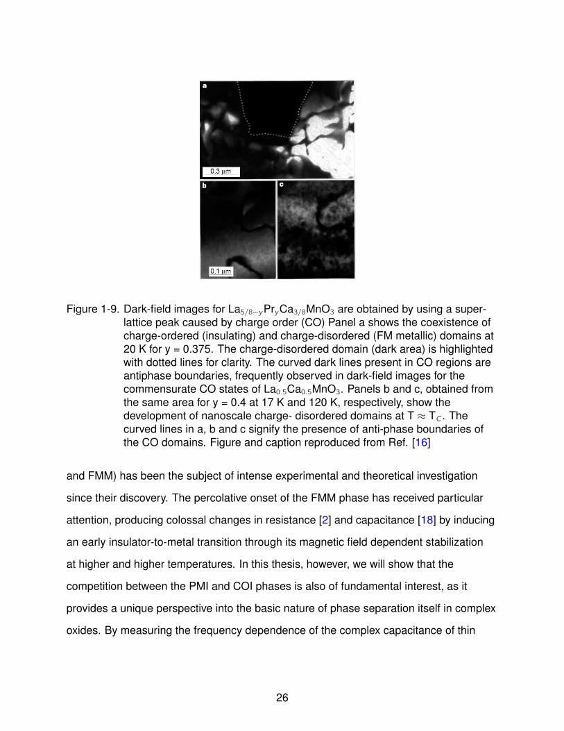
Figure 1-9. Dark-field images for La5/8−yPryCa3/8MnO3 are obtained by using a super-lattice peak caused by charge order (CO) Panel a shows the coexistence ofcharge-ordered (insulating) and charge-disordered (FM metallic) domains at20 K for y = 0.375. The charge-disordered domain (dark area) is highlightedwith dotted lines for clarity. The curved dark lines present in CO regions areantiphase boundaries, frequently observed in dark-field images for thecommensurate CO states of La0.5Ca0.5MnO3. Panels b and c, obtained fromthe same area for y = 0.4 at 17 K and 120 K, respectively, show thedevelopment of nanoscale charge- disordered domains at T ≈ TC . Thecurved lines in a, b and c signify the presence of anti-phase boundaries ofthe CO domains. Figure and caption reproduced from Ref. [16]
and FMM) has been the subject of intense experimental and theoretical investigation
since their discovery. The percolative onset of the FMM phase has received particular
attention, producing colossal changes in resistance [2] and capacitance [18] by inducing
an early insulator-to-metal transition through its magnetic field dependent stabilization
at higher and higher temperatures. In this thesis, however, we will show that the
competition between the PMI and COI phases is also of fundamental interest, as it
provides a unique perspective into the basic nature of phase separation itself in complex
oxides. By measuring the frequency dependence of the complex capacitance of thin
26
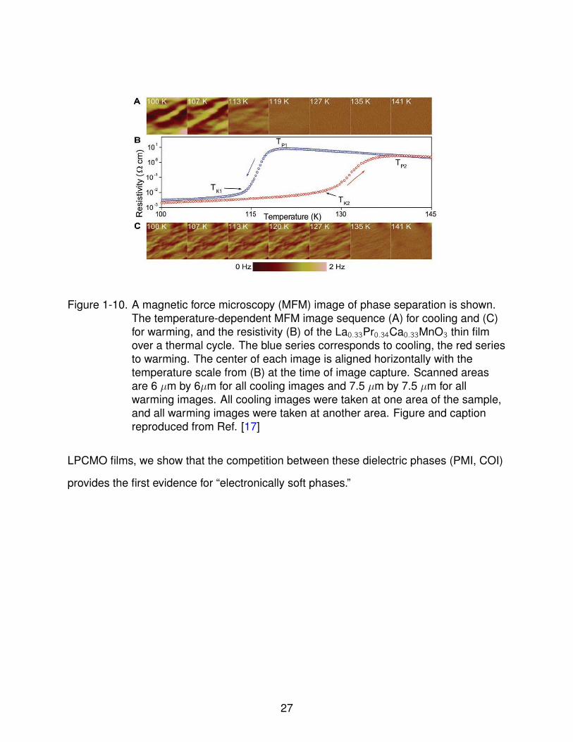
Figure 1-10. A magnetic force microscopy (MFM) image of phase separation is shown.The temperature-dependent MFM image sequence (A) for cooling and (C)for warming, and the resistivity (B) of the La0.33Pr0.34Ca0.33MnO3 thin filmover a thermal cycle. The blue series corresponds to cooling, the red seriesto warming. The center of each image is aligned horizontally with thetemperature scale from (B) at the time of image capture. Scanned areasare 6 µm by 6µm for all cooling images and 7.5 µm by 7.5 µm for allwarming images. All cooling images were taken at one area of the sample,and all warming images were taken at another area. Figure and captionreproduced from Ref. [17]
LPCMO films, we show that the competition between these dielectric phases (PMI, COI)
provides the first evidence for “electronically soft phases.”
27
1.2 Multiferroics
1.2.1 Introduction
Multiferroics - defined as materials possesing at least two ferroic orderings [19] -
have quickly become one of the most widely researched topics in condensed matter
physics today, both for their potential applications and for their complex physical origins.
Ferromagnetism, ferroelectricity, and ferroelasticity are the classic ferroic orders,
however, contemporary focus has placed little emphasis on ferroelastic properties, and
the magnetic ferroic requirements have been broadened to include antiferromagnetism
and ferrotoroidic orderings. The first attempts to combine multiple ferroic properties
into one material started in the 1960’s by Smolenskii and Venevtsev [20, 21]. Initially,
these results inspired moderate interest in the physics community, but multiferroics have
recently undergone an intense renaissance [22–26].
The multiferroic renaissance has been fueled by multiple factors. First in 2000,
a seminal paper highlighted the curious (and inconvenient) lack of overlap between
ferromagnetic and ferroelectric materials, resulting in a dearth of single-phase
multiferroics [27]. This paper in effect issued a grand challenge to materials development
which - thanks to recent advancements in both theoretical and experimental tools - has
been aggressively (and sucessfully) pursued. Experimentally, thin film crystal growth
has progressed significantly since the initial multiferroic interest of the 1960’s, with the
advent of strain engineering through epitaxial lattice mismatch and new high-pressure
growth techniques [28, 29]. Additionally, new experimental techniques for observing
electric and magnetic domains have developed [30]. Theoretically, improvements in
first-principles and density functional theory (DFT) computational techniques have
provided insight into relevant microscopic mechanisms promoting ferromagnetism,
ferroelectricity, and their couplings. Most important, however, is the growing intersection
of experiment and theory in multiferroics - where the newfound attainability of high
quality samples creates synergy through the direct feedback between both disciplines.
28

Finally, the multiferroic renaissance has been motivated by a broad realization of
potential applications for multiferroic materials. Ferromagnets are ubiquitous in the
transformer and information storage industries, and the sensing and actuation industries
rely heavily on ferroelectrics. With the strong trend toward device miniaturization,
the potential of combining multiple functionalities into a single material has made
single-phase multiferroics highly desirable. Multiferroics can also display strong
couplings in their ferroic orders, providing a large design space which will inevitably
lead to higher efficiencies and increased capabilities (see Fig. 1-11). Coupling between
elastic and ferroic properties is widely observed in the form of piezoelectricity and
piezomagnetism, where strain can induce electric or magnetic polarization (and vice
versa). However, the most interesting coupling is between the electric and magnetic
orderings themselves: magnetoelectric coupling - for a complete discussion of
magnetoelectric coupling see Sec. 1.3
This section will cover the basic physics of multiferroics, beginning with the two most
popular ferroic orderings: ferromagnetism and ferroelectricity. This leads to a discussion
of “d0-ness,” and their seemingly incompatible mechanisms. Finally we discuss novel
approaches to combine ferromagnetism and ferroelectricity in a single material.
1.2.2 Ferromagnetism
Magnetism is one of the most ancient physical phenomenon know to man, and was
first discussed scientifically in Greece more than 2500 years ago. Since then, multiple
types of magnetic ordering have been identified: diamagnetism, paramagnetism,
ferromagnetism, ferrimagnetism, antiferromagnetism, and canted antiferromagnetism
(see Fig. 1-12). Diamagnetic systems exhibit magnetizations (coherent orientations
of internal magnetic moments) which can be induced under external fields, with
the magnetization linearly proportional to the magnitude of applied field and aligned
anti-parallel to the field. Paramagnetic systems exhibit induced magnetizations under
external fields, with the magnetization linearly proportional to the magnitude of applied
29
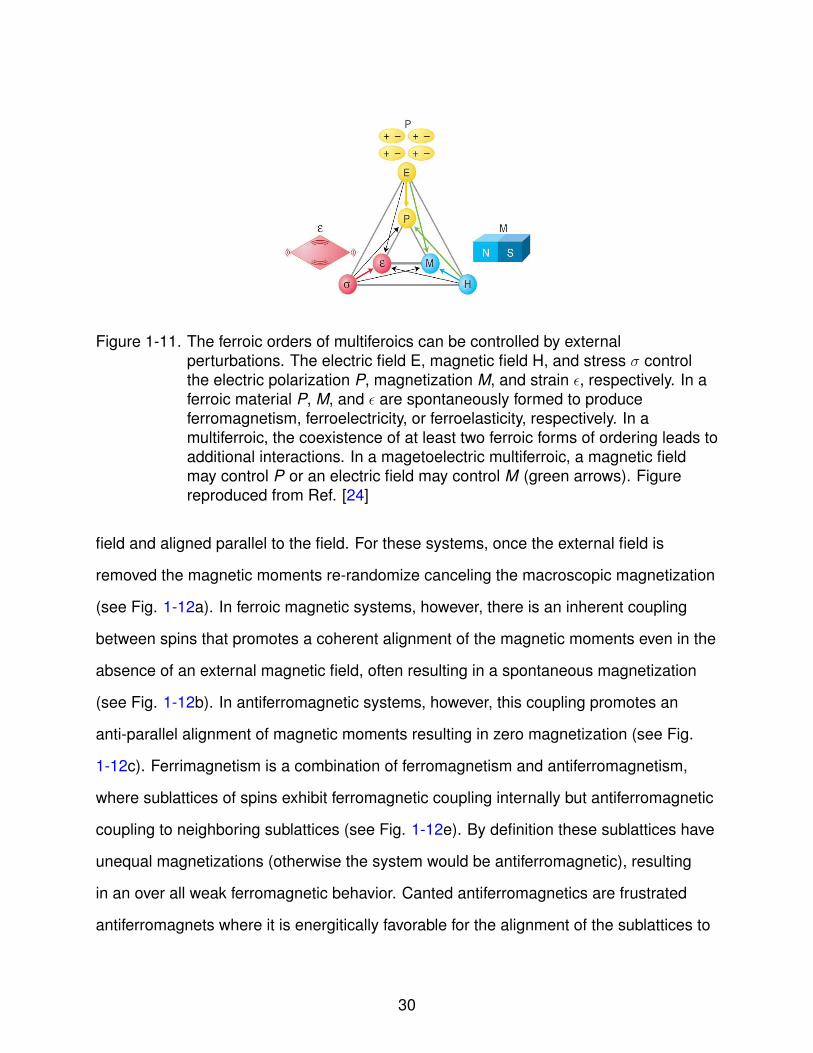
Figure 1-11. The ferroic orders of multiferoics can be controlled by externalperturbations. The electric field E, magnetic field H, and stress σ controlthe electric polarization P, magnetization M, and strain ε, respectively. In aferroic material P, M, and ε are spontaneously formed to produceferromagnetism, ferroelectricity, or ferroelasticity, respectively. In amultiferroic, the coexistence of at least two ferroic forms of ordering leads toadditional interactions. In a magetoelectric multiferroic, a magnetic fieldmay control P or an electric field may control M (green arrows). Figurereproduced from Ref. [24]
field and aligned parallel to the field. For these systems, once the external field is
removed the magnetic moments re-randomize canceling the macroscopic magnetization
(see Fig. 1-12a). In ferroic magnetic systems, however, there is an inherent coupling
between spins that promotes a coherent alignment of the magnetic moments even in the
absence of an external magnetic field, often resulting in a spontaneous magnetization
(see Fig. 1-12b). In antiferromagnetic systems, however, this coupling promotes an
anti-parallel alignment of magnetic moments resulting in zero magnetization (see Fig.
1-12c). Ferrimagnetism is a combination of ferromagnetism and antiferromagnetism,
where sublattices of spins exhibit ferromagnetic coupling internally but antiferromagnetic
coupling to neighboring sublattices (see Fig. 1-12e). By definition these sublattices have
unequal magnetizations (otherwise the system would be antiferromagnetic), resulting
in an over all weak ferromagnetic behavior. Canted antiferromagnetics are frustrated
antiferromagnets where it is energitically favorable for the alignment of the sublattices to
30

Figure 1-12. A sampling of magnetic order is shown. A) Paramagnetism: Magneticmoments are randomized for no net magnetization in zero external field. B)Antiferromagnetism: Magnetic moments are ordered in sublattices whichare anti-aligned with each other resulting in no net magnetization. C)Ferromagnetism: Magnetic moments are aligned parallel producing a largenet magnetization in zero external field. D) Canted-antiferromagnetism:Magnetic moments are ordered in sublattices which are only partiallyanti-aligned, producing a net magnetization (to the right here). E)Ferrimagnetism: Magnetic moments are ordered in sublattices which areanti-aligned, but unequal, resulting in a net magnetization.
skew from the 180o anti-parallel alignment, resulting in a small net magnetization (see
Fig. 1-12d).
At high temperatures, ferroic magnetic systems are typically paramagnetic before
undergoing a time-reversal invariance breaking transition at lower temperatures (the
Curie temperature, TC , for ferromagnetics; the Neel temperature, TN , for antiferromagnetics)
with the onset of magnetic coupling and the manifestation of spontaneous ordering.
Experimentally, in ferromagnets this transition is observed by the opening of magnetization
vs. magnetic field (M-H) hysteresis loops, see Fig. 1-13. Initially the system orders into
local domains which cancel globally to zero macroscopic magnetization. When a field of
sufficient strength is applied, the domains align and remain aligned after the removal of
31

M M
H
M
H H
HC
MS
T > TC T TC T < TC
Paramagnetic (PM) PM-FM Transition Ferromagnetic (FM)
M
H
Diamagnetic
Any T
A) D)C)B)
M M
H
M
H H
HC
MS
T > TC T TC T < TC
Paramagnetic (PM) PM-FM Transition Ferromagnetic (FM)
M
H
Diamagnetic
Any T
M M
H
M
H H
HC
MS
T > TC T TC T < TC
Paramagnetic (PM) PM-FM Transition Ferromagnetic (FM)
M
H
Diamagnetic
Any T
A) D)C)B)
Figure 1-13. M-H loops are shown for different magnetic orderings. A) Diamagnetism:M-H loop is closed, with a linearly induced magnetization that opposes theapplied field. B) Paramagnetism: M-H loop is closed, with a linearlyinduced magnetization aligned with the applied field. C) PM-FM transition:Near TC M-H loops begin to open with the onset of spontaneousmagnetization. D) Ferromagnetism: M-H loops are open, as there isspontaneous magnetization at zero external field (MS). MS can bereorientated under a “coercive” field, HC . Ferrimagnets andcanted-antiferromagnets have M-H loops similar to but smaller thanferromagnets.
the external field resulting in a large remanent spontaneous magnetization, MS (see Fig.
1-13). Ferrimagnets and canted antiferromagnets display reduced magnetic hysteresis
loops, however, pure antiferromagnets (with zero spontaneous magnetization) have no
magnetic hysteresis. Thus, ferromagnets are the most technologically relevant magnetic
materials, and accordingly they have received the most attention in research. Two
phenomenological theories have successfully reproduced many of the properties of
ferromagnetism: the Curie-Weiss local-moment theory, and the Stoner band theory of
ferromagnetism.
32

In 1907, Weiss developed a theory proposing that there existed some internal
“molecular field” which intrinsically aligned the individual magnetic moments of a
ferromagnet (which is now interpreted as an exchange interaction). At high temperatures
the thermal fluctuations were thought to be larger than the alignment energy of the
“molecular field,” resulting in randomized orientations of the magnetic moments and
the observed paramagnetic behavior. Below the Curie temperature, TC , the magnetic
alignment energy dominated, producing a coherent reorientation of the magnetic
moments and creating spontaneous magnetization. The Weiss local-moment theory
predicts the temperature dependence of the magnetic susceptibility for magnetic
materials according to the Curie-Weiss law:
χ =C
(T − TC)γ (1–3)
where C is the Curie constant, T and TC (the Curie temperature) are measured in
Kelvins, and γ is a critical exponent. The Curie-Weiss law accurately captures the
the high temperature behavior of ferro-, ferri-, and anti-ferromagnets, as well as the
divergence in susceptibility near TC in ferromagnets. However, the theory has two
shortcomings, namely: the theory requires the dipole moment at each site be equal in
both the paramagnetic phase and the ferromagnetic phase, and the theory also requires
the moments at each site to correspond to an integer number of electrons - neither of
which is observed experimentally. These contradictions, however, are resolved by the
Stoner band theory of ferromagnetism.
The Stoner band theory of ferromagnets is also derived from an exchange
interaction between magnetic moments. The exchange energy is minimized when
all magnetic moments are aligned parallel, however, opposing this energy gain is the
band energy required for electrons to occupy energy states higher than the nominally
degenerate anti-parallel states. The increased band energy is the primary obstacle to
magnetic order in most materials. For ferromagnetic transition metals, such as Fe, Ni,
33

and Co, the Fermi energy lies in a region of overlap between 3d and 4s orbital bands
causing the valence electrons to partially occupy both bands. The 4s bands have a low
density of states over a large energy range, meaning that to further populate this band
the electrons would have to reach to much higher energy states, as low levels fill quickly.
This large energy cost renders the energy gain from exchange coupling insignificant.
The 3d band, however, has a narrow but large density of states near the Fermi level -
meaning the cost of populating higher energy levels is much lower, and the energy gain
from exchange coupling becomes relevant again.
The exchange interaction can be thought of as shifting the 3d minority spin band
up in energy, see Fig. 1-14. The magnitude of the shift is uniform for all wavevectors,
resulting in a rigid displacement between minority and majority spin carriers. When the
Fermi level lies within the 3d band this results in an increased population of majority
spin carriers, and a spontaneous magnetization: M = µB(n↑-n↓), where n↑ and n↓ are the
majority and minority populations, respectively (see red and blue areas in Fig. 1-14),
and µB is the Bohr magneton. By incorporating Fermi statistics, this model succinctly
resolves the observation that magnetic moments do not correspond to integer numbers
of electrons, as well as the potential change of magnetic moments as energies change
during phase transitions. The model also explains the trend of ferromagnetism in
transition metals: in later transition metals the Fermi level rises above the 3d bands
causing both spin bands to be occupied equally, canceling the net magnetization.
Hence, for transition metal ions, ferromagnetism requires a partially occupied 3d band.
1.2.3 Ferroelectricity
Ferroelectricity was first discovered in 1920, in the Rochelle salt compound
(KNa(C4H4O6)•4H2O) [31], and since then numerous similarities to ferromagnetism
have been documented. Analogous to the energy gain from exchange coupling in
ferromagnetism, ferroelectricity is commonly driven by an energy gain associated
with the hybridization of ionic orbitals. Like in magnetism, there are multiple electronic
34
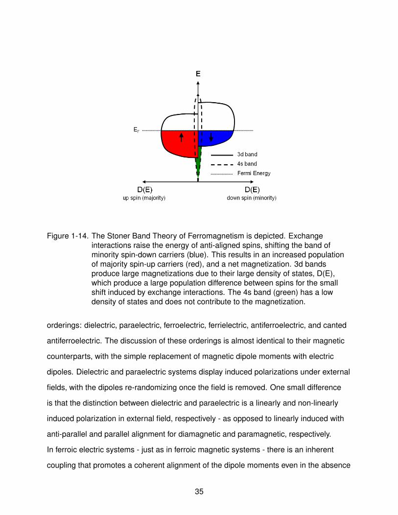
Figure 1-14. The Stoner Band Theory of Ferromagnetism is depicted. Exchangeinteractions raise the energy of anti-aligned spins, shifting the band ofminority spin-down carriers (blue). This results in an increased populationof majority spin-up carriers (red), and a net magnetization. 3d bandsproduce large magnetizations due to their large density of states, D(E),which produce a large population difference between spins for the smallshift induced by exchange interactions. The 4s band (green) has a lowdensity of states and does not contribute to the magnetization.
orderings: dielectric, paraelectric, ferroelectric, ferrielectric, antiferroelectric, and canted
antiferroelectric. The discussion of these orderings is almost identical to their magnetic
counterparts, with the simple replacement of magnetic dipole moments with electric
dipoles. Dielectric and paraelectric systems display induced polarizations under external
fields, with the dipoles re-randomizing once the field is removed. One small difference
is that the distinction between dielectric and paraelectric is a linearly and non-linearly
induced polarization in external field, respectively - as opposed to linearly induced with
anti-parallel and parallel alignment for diamagnetic and paramagnetic, respectively.
In ferroic electric systems - just as in ferroic magnetic systems - there is an inherent
coupling that promotes a coherent alignment of the dipole moments even in the absence
35
P P
E
P
E E
EC
PS
T > TC T TC T < TC
Paraelectric (PE) PE-FE Transition Ferroelectric (FE)P
E
Dielectric
Any T
A) D)C)B)
P P
E
P
E E
EC
PS
T > TC T TC T < TC
Paraelectric (PE) PE-FE Transition Ferroelectric (FE)P
E
Dielectric
Any T
A) D)C)B)
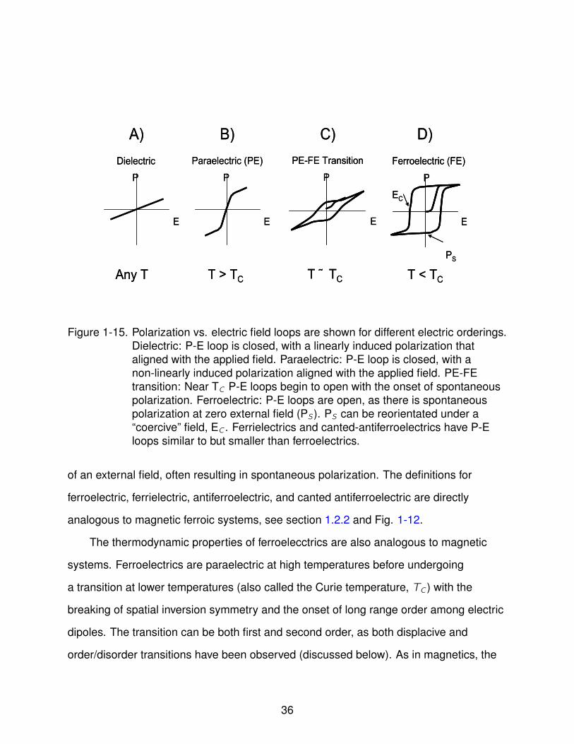
Figure 1-15. Polarization vs. electric field loops are shown for different electric orderings.Dielectric: P-E loop is closed, with a linearly induced polarization thataligned with the applied field. Paraelectric: P-E loop is closed, with anon-linearly induced polarization aligned with the applied field. PE-FEtransition: Near TC P-E loops begin to open with the onset of spontaneouspolarization. Ferroelectric: P-E loops are open, as there is spontaneouspolarization at zero external field (PS). PS can be reorientated under a“coercive” field, EC . Ferrielectrics and canted-antiferroelectrics have P-Eloops similar to but smaller than ferroelectrics.
of an external field, often resulting in spontaneous polarization. The definitions for
ferroelectric, ferrielectric, antiferroelectric, and canted antiferroelectric are directly
analogous to magnetic ferroic systems, see section 1.2.2 and Fig. 1-12.
The thermodynamic properties of ferroelecctrics are also analogous to magnetic
systems. Ferroelectrics are paraelectric at high temperatures before undergoing
a transition at lower temperatures (also called the Curie temperature, TC ) with the
breaking of spatial inversion symmetry and the onset of long range order among electric
dipoles. The transition can be both first and second order, as both displacive and
order/disorder transitions have been observed (discussed below). As in magnetics, the
36

Figure 1-16. Ferroelectric Bananas. A) Charge versus voltage loop typical for a lossydielectric, in this case the skin of a banana B) electroded using silver paste.The hysteresis loop for a truly ferroelectric material such as Ba2NaNb5O15C) is shown in D) ferroelectric hysteresis curve for ceramic barium sodiumniobate. Figure and caption reproduced from Ref. [32].
most common technique for observing ferroelectric transitions is hysteresis loops, here
polarization vs. electric field (P-E loops), which open near TC . Ferroelectric dipoles
also initially order into local domains, which can be aligned under a strong electric field
resulting in a remanent spontaneous polarization, PS , when the field is removed, see
Fig. 1-15d. The dipole moments in antiferroelectrics are anti-aligned resulting in zero
remanent polarization, while ferrielectrics and canted antiferroelectrics display weak
but open P-E loops. Unlike ferromagnetism, however, ferroelectric hysteresis loops are
constructed from transport measurements, making them susceptible to multiple potential
artifacts such as leakage and dielectric loss. To drive home this point, recently one
researcher humorously demonstrated that transport measurements on a banana could
produce open P-E hysteresis loops similar to those reported in the literature, despite the
obvious absence of inherent ferroelectricty [32].
37

Early work on ferroelectrics centered around Rochelle salt which was useful
for identifying basic properties, however, its complex structure and large number of
atoms per unit cell prevented theoretical progress. Today, perovskite oxides with the
cubic ABO3 structure are the most widely studied ferroelectrics, and their simplified
structure has facilitated a theoretical understanding of fundamental ferroelectric
mechanisms. Below the Curie temperature, perovskite ferroelectrics undergo a
symmetry lowering distortion caused by the off-center shift of their B site cations,
which induces a spontaneous dipole moment (see Fig. 1-17). Ferroelectricity is the
result of a delicate balance between short-range repulsions which favor non-polar cubic
states, and long-range Coloumb forces which stabilize ferroelectric distortions. Density
functional theory has provided a significant contribution to the understanding of this
balance, as it has been clearly demonstrated that the off-center shifts are the result of
the hybridization of B site 3d orbitals with O 2p orbitals, which is essential to weaken
short-range repulsions and lowers the energy of the distorted ferroelectric state (see
Figs. 1-18 and 1-17).
The energy gain associated with this hybridization can also be described analytically
[26, 33]. Upon distortion, the hybridization matrix element tpd modifies to tpd(1 + gu)
where u is the distortion and g is the coupling constant. The first order terms in the
hybridization energy cancel, with the second order approximation producing an energy
gain:
δE ≈ −(tpd(1 + gu))2/∆− (tpd(1− gu))2/∆ + 2t2pd/∆ = −2t2pd(gu)2/∆ (1–4)
where ∆ is the charge transfer gap. This energy gain is depicted in Fig. 1-18a, where
the two O 2p electrons occupy a lower energy hybridized bonding state. However,
the energy gain associated with this hybridization is dependent on the valance of
the 3d orbital. If the 3d orbital contains an electron, then one electron is forced to
occupy the higher energy, anti-bonding hybridized state - lowering the energy gain and
38
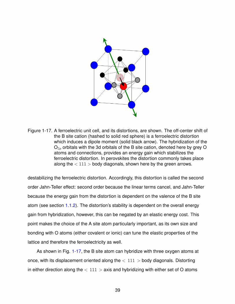
Figure 1-17. A ferroelectric unit cell, and its distortions, are shown. The off-center shift ofthe B site cation (hashed to solid red sphere) is a ferroelectric distortionwhich induces a dipole moment (solid black arrow). The hybridization of theO2p orbitals with the 3d orbitals of the B site cation, denoted here by grey Oatoms and connections, provides an energy gain which stabilizes theferroelectric distortion. In perovskites the distortion commonly takes placealong the < 111 > body diagonals, shown here by the green arrows.
destabilizing the ferroelectric distortion. Accordingly, this distortion is called the second
order Jahn-Teller effect: second order because the linear terms cancel, and Jahn-Teller
because the energy gain from the distortion is dependent on the valence of the B site
atom (see section 1.1.2). The distortion’s stability is dependent on the overall energy
gain from hybridization, however, this can be negated by an elastic energy cost. This
point makes the choice of the A site atom particularly important, as its own size and
bonding with O atoms (either covalent or ionic) can tune the elastic properties of the
lattice and therefore the ferroelectricity as well.
As shown in Fig. 1-17, the B site atom can hybridize with three oxygen atoms at
once, with its displacement oriented along the < 111 > body diagonals. Distorting
in either direction along the < 111 > axis and hybridizing with either set of O atoms
39

b)
A) B)
Figure 1-18. Ferroelectric Energy Diagrams. A) This hybridization energy diagramshows the energy gain from hybridizing O2p and B site 3d orbitals when the3d orbital is empty. When the 3d orbital is occupied (shown here withdashed arrows), its electron(s) must occupy the anti-bonding hybridizationstate, lowering the energy gain. B) This potential energy diagram shows thedouble well associated with hybridizing with both sets oxygen along the< 111 > body diagonal.
results in an identical energy gain, leading to a double well potential (see Fig. 1-18b).
This double well results in the characteristic “switchable” ferroelectric states, as opposite
distortions invert the induced dipole moment (and therefore the bulk polarization vector).
In the order/disorder interpretation, the B site cations are displaced along the body
diagonals, producing (microscopic) spontaneous dipole moments at every temperature.
At high temperatures, all eight dipole orientations are stable - which when averaged
across the sample results in zero net polarization. Then near TC the dipoles adopt either
the same orientation (rhombohedral symmetry) or two or three preferred orientations
(tetragoal or orthorhombic symmetry). The order/disorder model therefore predicts
a second order transition. Alternatively, the soft-mode model predicts a first order
transition. In the soft-mode interpretation, B site displacements are only stable below
TC . At higher temperatures, phonon modes provide a restoring force that eliminates the
40

displacement. According to the model, as temperature is reduced the frequency of the
phonon mode “softens,” decreasing to zero at TC resulting in a static ferroelectric lattice
deformation that extends throughout the crystal, and a first order volume change.
When ferroelectricity occurs via an off-center shift of the B site cation, as described
above, it is deemed ‘proper’ ferroelectricity. However, as long as inversion symmetry is
broken, there are multiple ‘improper’ mechanisms which can produce ferroelectricity.
The renaissance of multiferroics has led to the discovery of multiple new ‘improper’
ferroelectric mechanisms: interfacial effects, charge-frustration, bonding distributions,
lone-pairs, and magnetic interactions/orderings. In short-period superlattices it has
been shown that interfacial effects can break inversion symmetry through cooperative
rotations of oxygen octahedra, which produce a spontaneous electric dipole moment
[34]. Charge-frustration based ferroelectricity has been demonstrated in charge-ordered
systems with triangular lattices which introduce geometric frustration, here the
lattice is centrosymmetric, and it is the asymmetric charge distribution that breaks
inversion symmetry [29]. It was also shown that the coexistence of bond-centered and
site-centered charge orders in half-doped Pr1−xCaxMnO3 leads to a non-centrosymmetric
charge distribution and a net electric polarization [35]. Additionally, A site cations with
lone-pairs have been shown to induce ferroelectricity even when their corresponding
B site cations have partially filled 3d orbitals (see Section 1.2.2). However, despite
these promising avenues, magnetic ferroelectric mechanisms have received the most
attention.
Magnetic mechanisms began receiving attention after the popular report of a
spin-flop transition in TbMnO3 where a magnetic field of ≈ 5T was shown to rotate
the ferroelectric polarization 90o from the a-axis to the c-axis, as well as increase the
dielectric constant as much as 500% [28]. Interestingly, these phenomena were linked
to the magnetic frustration. It has been shown that inhomogeneous magnetic order
allows for third-order free-energy terms of the form PM∂M. In cubic crystals this results
41

Figure 1-19. This figure shows the effects of the antisymmetric DzyaloshinskiiMoriyainteraction. The interaction HDM = D12· [S1×S2]. The Dzyaloshinskii vectorD12 is proportional to spin-orbit coupling constant λ, and depends on theposition of the oxygen ion (open circle) between two magnetic transitionmetal ions (filled circles), D12 ∝ λx×r12. Weak ferromagnetism inantiferromagnets (for example, LaCu2O4 layers) results from the alternatingDzyaloshinskii vector, whereas (weak) ferroelectricity can be induced by theexchange striction in a magnetic spiral state, which pushes negativeoxygen ions in one direction transverse to the spin chain formed by positivetransition metal ions. Figure and caption reproduced from Ref. [22]
in polarization of the form [36]:
P = [(M · ∂)M−M(∂ ·M)]. (1–5)
Magnetic frustration induces spatial variations in magnetization, thereby inducing a
polarization through ∂M. Ferromagnetic interactions (J > 0) between neighboring spins,
with antiferromagnetic interactions (J’ < 0) between next nearest neighbors can induce
spiral magnetic states of the form:
Sn = S [cos(qxxn)x+ sin(qyxn)y], (1–6)
42
where q is a wavevector determined by the ratio of ferromagnetic and antiferromagnetic
interactions. In addition to breaking time-reversal symmetry, this ordering simultaneously
breaks inversion symmetry because the change of the sign of all coordinates inverts
the direction of the rotation of spins in the spiral. According to Eq. 1–5, this produces
a polarization orthogonal to both q and z : P || z × q. A likely microscopic mechanism
for this ferroelectric polarization is the anti-symmetric Dzyaloshinskii-Moriya (DM)
interaction. The DM interaction is a relativistic correction to superexchange, and can
be written: Dn,n+1· Sn× Sn+1, where Dn,n+1 is the Dzyaloshinskii vector - which is
proportional to x× rn,n+1, where rn,n+1 is a unit vector along the line connecting the
magnetic ions, and x is the displacement of the oxygen ion from this line. In spiral
magnets, the product Sn× Sn+1 in the DM interaction has the same sign for all pairs and
uniformly pushes negative oxygen ions in one direction perpendicular to the spin chain
composed of positive magnetic ions, thus creating polarization perpendicular to the
chain.
1.2.4 Magnetoelectric Multiferroics
Magnetoelectric multiferroics are materials that are simultaneously ferromagnetic
and ferroelectric - and also display coupling between the ferroic orders (see section
1.3). Accordingly, for a material to display both orderings it is subject to the physical,
structural, and electrical constraints required for both ferroic properties. These
constraints include: symmetry, electrical conduction, and orbital chemistry. Ferroelectric
polarization requires a low symmetry structure which breaks inversion symmetry, and
ferromagnetic polarization requires a low symmetry structure which breaks time-reversal
symmetry. There are 31 point groups which allow spontaneous ferroelectric polarization,
and there are also 31 point groups which allow spontaneous ferromagnetic polarization.
Of these two sets of point groups, 13 overlap - allowing both electric and magnetic
spontaneous polarizations [19]. With the initial number of Shubnikov point groups
at 122, reducing to 13 point groups appears to be a strong limitation. However,
43

considering that there are multiple materials within these 13 point groups which are
not magnetoelectric multiferroics, clearly additional limitations play an important role.
The electrical constraint is that ferroelectric materials must be insulating, as free charge
carriers would immediately screen the spontaneous electric polarizaiton rendering the
ferroelectricity undetectable. This is an important point because empirically almost all
ferromagnets are metallic. Despite these important factors, however, one constraint has
proved to be the most dominant: orbital chemistry.
As discussed in Sections 1.2.2 and 1.2.3 orbital chemistry plays a vital role in the
primary mechanisms for both ferromagnetism and ferroelectricity. In the Stoner band
theory of ferromagnetism, a partially full 3d orbital with exchange interactions between
spins shifts the population balance of spin-up and spin-down electrons resulting in
a net magnetization. Ferroelectricity, however, typically relies on the hybridization of
empty 3d orbitals with O2p orbitals producing an off-center shift of the B site cation which
breaks inversion symmetry and induces a net spontaneous electric dipole moment.
Therefore, the fundamental mechanisms for the two ferroic orderings seem to be
mutually exclusive, requiring both empty 3d orbitals for ferroelectricity (termed d0-ness)
and paritally full 3d orbitals for ferromagnetism. While it has been demonstrated that
ferroelectricity can also be established via ‘improper’ mechanisms (see Section 1.2.3),
it is certainly true that these conflicting processes strongly limit the coexistence of
ferromagnetism and ferroelectricity making single-phase magnetoelectric multiferroics
exceptionally rare.
The first attempts to bypass this mutual exclusion involved constructing elaborate
materials which included separate structural units to produce the individual ferroic
properties. These attempts centered around materials with BO3 groups, such as
GdFe3(BO3)4 and Ni3B7O13I, and were successful in producing multiferroic properties
[37]. However, due to the isolation of the ferromagnetic and ferroelectric components,
coupling between the ferroic orders was extremely limited. With the recent improvement
44

B)A)
Figure 1-20. Composite Multiferroic Geometries. A) Composite multiferroic can begrown in a horizontal laminated structure of epitaxial layers grownsuccessively. b) Composite multiferroic can be also grown in a verticalcolumnar structure with self organizing columns of one ferroic materialinside a parent matrix of another.
in thin film growth techniques, modern efforts have focused on nanoscale heterostructures.
Both horizontal heterostructures composed of alternating layers of ferromagnetic and
ferroelectric compounds, and vertical heterostructures composed of self-assembled
nano-pillars inside parent matrices have been investigated [38, 39]. When the
ferromagnetic and ferroelectric compounds are also piezoelectric and piezomagnetic (or
electrostrictive and magnetostrictive) this geometry produces efficient magnetoelectric
coupling mediated by strain. Here, applied electric (magnetic) fields induce a mechanical
strain in the piezoelectric (piezomagnetic) layers which, through the epitaxial growth
conditions, additionally strains the piezomagnetic (piezoelectric) layers producing
a magnetic (electric) polarization. The composite approach has proven successful
for several niche technological applications such as microwave applications and
high-resolution magnetic field sensors, however, it fails to encompass the full vision
of magnetoelectric multiferroics.
45

Composites fall short in terms of both technology and physics. Technologically,
stacking/mixing ferroic layers and coupling them via strain is incapable of producing the
properties needed for emerging technologies such as spintronics and tunnel junctions.
True magnetoelectric multiferroics are prime candidates for spintronic applications
because they are magnetic insulators in which the band gap may be tuned by the
orientations of the ferroelectric polarization. This is useful because when the band gap
is large, only majority spins can tunnel through the barrier creating a spin-filter which
passes spin-polarized currents. When the gap is reduced, the spin-polarization of the
current decreases and the spin-filter can essentially be switched “off.” Alternatively,
composites cannot emulate this functionality because the ferroelectric components
are not magnetic and spins decohere traveling through these layers. Physically, the
composite shortcut offers little insight into fundamental principles of the compatibility of
ferromagnetism and ferroelectricity. Multiferroics present condensed matter physics a
challenging puzzle, the solution of which could teach us valuable lessons about two of
the most technologically relevant material properties known. Additionally, isolating the
interaction between ferroic properties to the interfaces limits the ability to learn about
inherent couplings between them. Thus, the study of single-phase magnetoelectric
multiferroics is important, both technologically and physically.
Several single-phase magnetoelectric multiferroics have recently been discovered
thanks to ‘improper’ ferroelectric mechanisms (see Section 1.2.3). Frustrated magnets
where the spatial variation in magnetization breaks inversion symmetry have emerged
as a ferroic hotbed. Here, because the ferroelectricity is caused by the magnetic
ordering, it is particularly sensitive to magnetic fields leading these systems to have
displayed the largest magnetoelectric coupling observed in single phases to date.
Unfortunately, the coupling is unidirectional as electric fields have no effect on magnetic
properties, limiting their potential application. However, another approach has also
proved promising: Bi based multiferroics. In Bi based multiferroics, the Bi ion contains
46
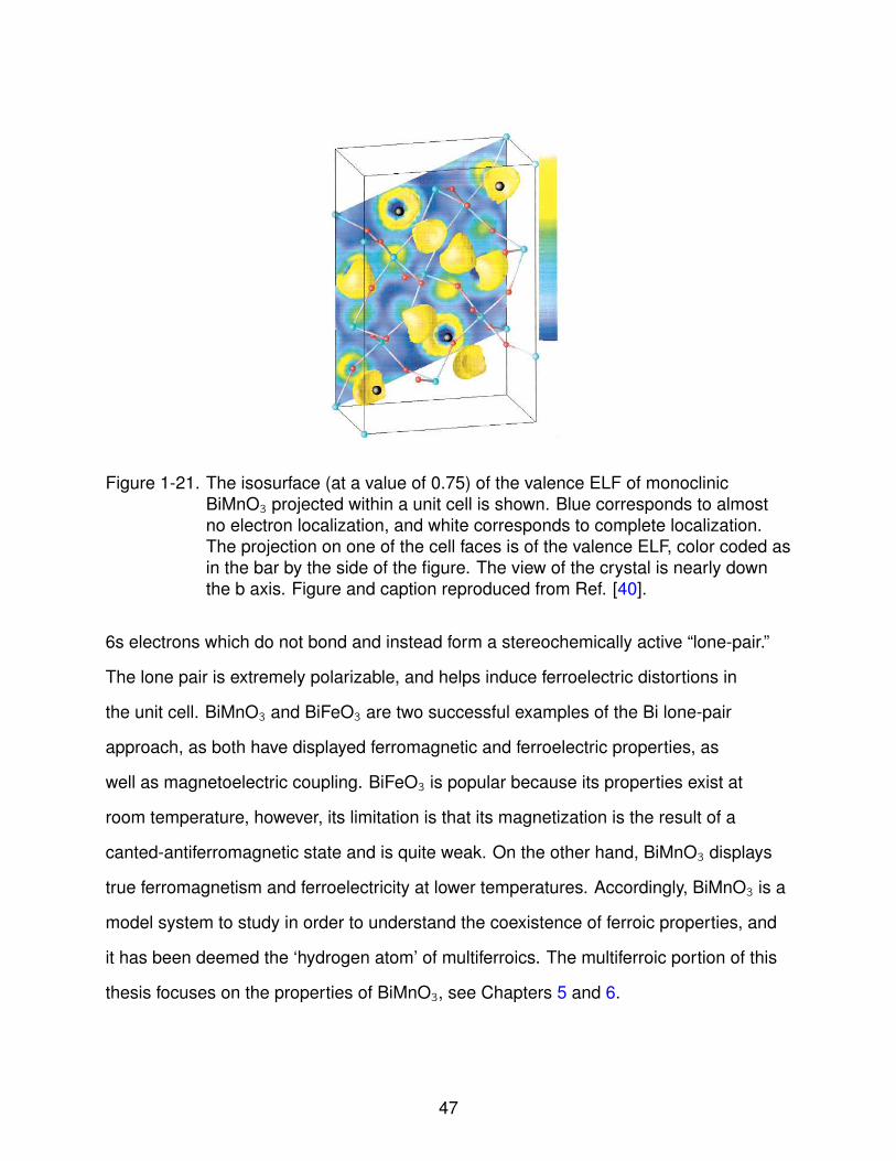
Figure 1-21. The isosurface (at a value of 0.75) of the valence ELF of monoclinicBiMnO3 projected within a unit cell is shown. Blue corresponds to almostno electron localization, and white corresponds to complete localization.The projection on one of the cell faces is of the valence ELF, color coded asin the bar by the side of the figure. The view of the crystal is nearly downthe b axis. Figure and caption reproduced from Ref. [40].
6s electrons which do not bond and instead form a stereochemically active “lone-pair.”
The lone pair is extremely polarizable, and helps induce ferroelectric distortions in
the unit cell. BiMnO3 and BiFeO3 are two successful examples of the Bi lone-pair
approach, as both have displayed ferromagnetic and ferroelectric properties, as
well as magnetoelectric coupling. BiFeO3 is popular because its properties exist at
room temperature, however, its limitation is that its magnetization is the result of a
canted-antiferromagnetic state and is quite weak. On the other hand, BiMnO3 displays
true ferromagnetism and ferroelectricity at lower temperatures. Accordingly, BiMnO3 is a
model system to study in order to understand the coexistence of ferroic properties, and
it has been deemed the ‘hydrogen atom’ of multiferroics. The multiferroic portion of this
thesis focuses on the properties of BiMnO3, see Chapters 5 and 6.
47

1.3 Magnetoelectric Coupling
1.3.1 Introduction
Magnetoelectric coupling has also undergone an intense revival [41], as shown
in Fig. 1-22, where the number of publications citing ‘magnetoelectric’ as a keyword
is shown to have increased exponentially over the past 20 years. Initially, interest in
magnetoelectric coupling started modestly, with the first experimental observations
and theoretical predictions dating as far back as the 1800’s. In 1888, Rontgen found
that when a dielectric was placed in motion in an external electric field it became
magnetized - soon followed by the observation of the reverse effect (polarization of
a moving dielectric in a magnetic field) [42, 43]. Then in 1894 Curie provided the
first theoretical description of the potential for static magnetoelectric coupling on the
basis of symmetry. Much later, it was realized that magnetoelectric coupling was
only possible in materials which break time-reversal symmetry, such as: materials in
motion, materials in the presence of magnetic fields, or materials with intrinsic magnetic
ordering. Finally, in the late 1950’s a linear magnetoelectric effect based on the violation
of time-reversal symmetry was predicted by Dzyaloshinskii in a specific static material,
Cr2O3, which was followed shorty by the experimental observation of its electric field
induced magnetization. These findings galvanized the physics community briefly,
however, a general weakness of the coupling, a dearth of systems displaying it, and
a limited understanding of the microscopic mechanisms led to a decreased interest in
magnetoelectric phenomena.
After a 20 year lull, the field has been reignited in response the recent developments
in multiferroic research. Magnetoelectric coupling of as many as 5 orders of magnitude
larger than that observed in Cr2O3 has been achieved in composites of piezoelectric
and piezomagnetic materials, with strain inducing polarizations in each component.
Single-phase multiferroics have also shown great potential, where fundamental
limitations on the magnitude of magnetoelectric coupling have been shown to be
48
Figure 1-22. This figure shows the publications per year with ‘magetoelectric’ as akeyword according to the Web of Science. Figure and caption reproducedfrom Ref. [41]
loosened in these systems (see Section 1.3.3). However, as shown by the venn
diagram of Fig. 1-23, magnetoelectric coupling is not limited to ferroic materials,
and this magnetoelectric ‘momentum’ has also spilled over into additional materials
research areas. In particular, the effect of magnetic fields on the electric properties of
correlated electron systems has become an extremely active area of research. Spin
offs of magnetoelectric couplings termed ‘magnetocapacitance’ and ‘magnetodielectric’
have become ubiquitous, exemplified by report of colossal magnetoresistance and
magnetocapacitance in mixed valence manganites [18]. Magnetocapacitance was even
shown to be possible non-magnetic media as long as it is inhomogeneous [44]. Thus,
the search for magnetic field induced electric polarization has been reinvigorated, and
has expanded to multiple new landscapes.
Finally, it should be noted that the current revival is also due to a long list of
potential technological applicaitons for magnetoelectric coupling. Although many
of these concepts were conceived following the initial research surge, the recent
progress has made the realization of their potential tantalizingly close. In particular,
magnetoelectric coupling could one day lead to the writing and reading of magnetic data
with electric fields, a capability that would decrease the power usage and increase the
49

Figure 1-23. This figure shows the relationship between multiferroic and magnetoelectricmaterials. Ferromagnets (ferroelectrics) form a subset of magnetically(electrically) polarizable materials such as paramagnets andantiferromagnets (paraelectrics and antiferroelectrics). The intersection(red hatching) represents materials that are multiferroic. Magnetoelectriccoupling (blue hatching) is an independent phenomenon that can, but neednot, arise in and of the materials that are both magnetically and electricallypolarizable. In practice, it is likely to arise in all such materials, eitherdirectly or indirectly via strain. Figure and caption reproduced from Ref.[25]
speed of nearly every device involving memory. Additional devices proposed include
high-resolution magnetic field sensors, electrically tunable microwave applications such
as filters, oscillators and phase-shifters, and spintronic applications such as spin-wave
generation, amplification, and frequency conversion.
1.3.2 Maxwell Equations vs. Magnetoelectric Coupling
Classical electromagnetism is one of the most successful and influential branches
of physics in history. In 1865, Maxwell unified the theories of electric and magnetic
fields in four concise equations which now famously bear his name. These equations
predicted and explained an inherent coupling between electricity and magnetism - where
one changing field can induce the other - and successfully describe almost all physical
50

phenomena ruled by one of the four fundamental physical forces: the electromagnetic
interaction. Maxwell’s equations elegantly describe the nature of electric and magnetic
fields in vacuum (the propagation of light), and can even account for electric and
magnetic phenomena in polarizable media as well by introducing constitutive equations
(the electric displacement and magnetizing fields). Therefore, it is quite surprisingly that
the fundamental coupling between electricity and magnetism described by Maxwell’s
equations has little to offer in terms of magnetoelectric coupling.
The crux of the matter is that the coupling in Maxwell’s equations only deals with the
electric and magnetic fields and not the electric and magnetic polarization themselves.
In order to describe and understand magnetoelectric coupling, it is necessary to
understand how the polarization is induced. In solids, magnetic polarization is related
to the spins of electrons in partially filled orbitals and electric polarization results from
the covalently driven shifts of negative and positive ions. The constitutive equations of
classical electromagnetism are not equipped to describe either of these processes.
Quantum mechanics, on the other hand, has all the tools necessary to describe
the manifestations of polarization and their coupling. On the most fundamental level
the exchange interaction combines the electrostatic and magnetic interaction in solids.
The exchange interaction is strictly a quantum mechanical phenomenon which is a
geometric consequence of the symmetrization requirement, and therefore has no
classical counterpart. It determines the extent of the overlap of wavefunctions in real
space, and is also dependent on relative spin states. This directly affects the cooperative
alignment of electron spins and the charge distributions of electronic bonds, thereby
controlling the magnetization and charge separation (electric polarization).
Multiple microscopic mechanisms have been shown to modify these exchange
interactions and thereby indirectly affect magnetoelectric properties: single-ion
anisotropy (∝ (Szi )2), symmetric superexchange (∝ ri ,j(Sxi Syj + Syi Sxj )), antisymmetric
superexchange (∝ ri ,j(Sxi Syj −Syi Sxj )), dipolar interactions (∝ ~mi ~mi/r3i ,j−3( ~mi ~ri ,j)( ~mi ~ri ,j)/r 5i ,j),
51

and Zeeman energies (∝ BgiSi). Strain/stress is also an efficient mechanism to
modulate exchange interactions, because by changing crystal lattice constants the
overlap of electronic wavefunctions is directly affected. This strain can be applied
mechanically or via external fields, as described by Maxwell’s stress tensor.
1.3.3 Free Energy
Theoretically, ME coupling is typically described using Ginzburg-Landau theory,
where a free energy analysis provides a unified temperature and field dependence
of the thermodynamics and stability of the constituent electronic phases. The free
energy is commonly written phenomenologically as a series expansion in powers of the
magnetic and electric fields, ~H and ~E respectively:
− F (~E , ~H) = 12ε0εi ,jEiEj +
1
2µ0µi ,jHiHj + αi ,jEiHj +
βi ,j ,k2EiHjHk +
γi ,j ,k2HiEjEk + · · · (1–7)
where ε0 and µ0 are the permittivity and permeability of free space, εi ,j and µi ,j are the
relative permittivity and permeability, and α and β and γ are the phenomenological
magnetoelectric coupling constants. In this notation, polarizations can easily be
calculated as a function of applied fields,
Pi = (− ∂F
∂Ei) = ε0εi ,jEj + αi ,jHj +
βi ,j ,k2HjHk + · · · (1–8)
µ0Mi = (− ∂F
∂Hi) = µ0µi ,jHj + αi ,jEj +
βi ,j ,k2EjEk + · · · (1–9)
The free energy formalism is convenient because it also serves as an infrastructure
for testing specific microscopic coupling mechanisms, and multiple mechanisms have
been shown to produce ME coupling (see section 1.3.2). These mechanisms can then
be mapped onto the phenomenological expansion for systematic comparisons.
Analysis of the free energy has also provided important insight and guidelines to
researchers. In particular, it was shown that enforcing a stability condition on εi ,j and µi ,j
by requiring the sum of the first three terms in Eq. 1–7 to be greater than zero (ignoring
higher order coupling), the linear magnetoelectric coupling constant, αi ,j , is bounded by
52
the geometric mean of the diagonalized tensors εi ,j and µi ,j such that:
α2i ,j ≤ ε0µ0εi ,jµi ,j . (1–10)
This result is important because researchers knew to only investigate magnetoelectric
coupling in materials with large permittivities and permeabilities. In fact, this is the
reason that multiferroics are the most popular magnetoelectric materials - with
their typically large permittivities and permeabilities, they relax one of the strongest
constraints on magnetoelectric coupling.
53

CHAPTER 2EXPERIMENTAL TECHNIQUES
2.1 Sample Fabrication
2.1.1 Growth Methods
This thesis includes data from two types of thin film complex oxides:
(La1−yPry )1−xCaxMnO3 (LPCMO) and BiMnO3 (BMO). Both films were grown via pulsed
laser deposition (PLD) in Dr. Biswas’ lab. The growth is epitaxial (lattice matched),
where the structure of a thin (0.5 mm) single crystal substrate acts as a template for the
crystal structure of the film. The substrates used in this thesis were NdGaO3 and SrTiO3
for LPCMO and BMO respectively.
The PLD system is composed of a KrF excimer laser (248 nm), a vacuum chamber,
a target material, and a substrate heater. The laser is pulsed on and off, ablating the
target and creating a stoichiometric plume of the material’s elements that extends to just
above the substrate, resulting in the deposition of less than one monolayer per pulse.
The heater supplies the thermal energy necessary to allow the elements to shift into the
most energetically favorable configuration, resulting in the crystalline structure.
Careful optimization of multiple growth parameters was required to obtain
high-quality, stoichiometric, epitaxial, and crystalline samples. This optimization was
primarily performed by Dr. Tara Dhakal and Hyoungjeen Jeen of Dr. Biswas’ research
group for LPCMO and BMO respectively. For the LPCMO films the substrate was heated
to 820 oC in a vacuum of 10−6 Torr, then a partial pressure of oxygen of 450 mTorr was
applied during film growth with a laser pulse frequency of 5 Hz and laser energy of 480
mJ, with a pre-ablation period priming the target before a shutter guarding the sample is
removed. For the BMO films the substrate was heated to 632 oC (a lower temperature
than for LPCMO was necessary to avoid Bi evaporation) under a vacuum of 10−6, then
a partial pressure of oxygen of 37 mTorr was applied during film growth with laser pulse
frequency of 5 Hz and laser energy of 480 mJ. Additionally, the BMO films required a
54

B)A)
Figure 2-1. A) A schematic of PLD chamber is shown B) An image illustrating the plumecreated by the laser ablating the target during film growth (white) is shown.The tip of the outer edge of the plume very nearly coincides with the heater(red/orange, 820C) where the sample is mounted on the substrate, resultingin slow controlled growth. TheiImages were provided by Dr. Biswas.
non-stoichiometric target of Bi2.4MnO3 as well as an quenching oxygen pressure of 680
Torr during cooling. Film thicknesses ranged 30-150nm for LPCMO and 30-60 nm for
BMO.
For the LPCMO samples, a 10-15 nm capping dielectric layer of AlOx was grown
using rf magnetron sputtering of an alumnina target in an ultra-high vacuum chamber
with a base pressure of 10−9 Torr. Both LPCMO and BMO films also had top electrodes
deposited by thermal evaporation in a vacuum of 10−6 of high-quality metals held in
tungsten boats. The LPCMO electrodes were Al, deposited through a shadow-mask
to attain designed sizes and shapes. The BMO electrodes (Cr/Au) were an interdigital
array requiring multiple processing steps which are described in section 2.4.3.
2.1.2 Structural and Compositional Characterizations
The structure and composition of each film was confirmed using various X-ray
diffraction techniques. For LPCMO standard Θ − 2Θ X-ray diffraction measurements
were performed determining the samples were epitaxial and of a single chemical
phase [45]. For BMO, Θ − 2Θ X-ray diffraction and Auger electron spectroscopy
55
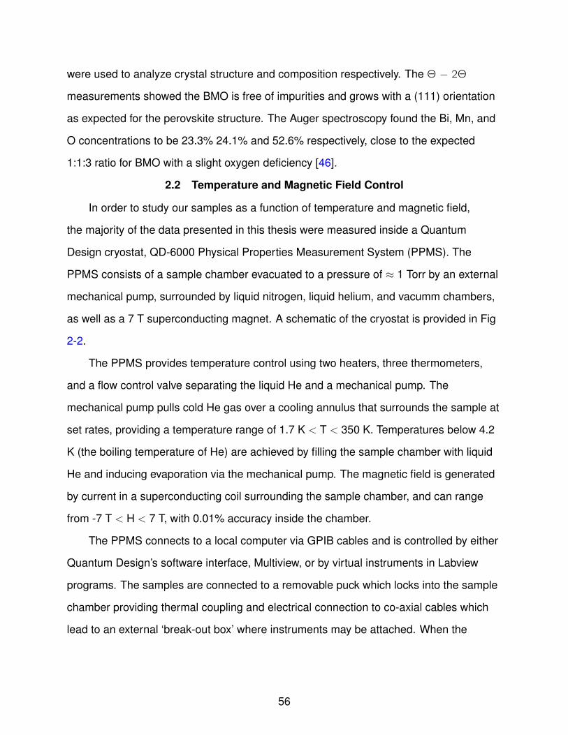
were used to analyze crystal structure and composition respectively. The Θ − 2Θmeasurements showed the BMO is free of impurities and grows with a (111) orientation
as expected for the perovskite structure. The Auger spectroscopy found the Bi, Mn, and
O concentrations to be 23.3% 24.1% and 52.6% respectively, close to the expected
1:1:3 ratio for BMO with a slight oxygen deficiency [46].
2.2 Temperature and Magnetic Field Control
In order to study our samples as a function of temperature and magnetic field,
the majority of the data presented in this thesis were measured inside a Quantum
Design cryostat, QD-6000 Physical Properties Measurement System (PPMS). The
PPMS consists of a sample chamber evacuated to a pressure of ≈ 1 Torr by an external
mechanical pump, surrounded by liquid nitrogen, liquid helium, and vacumm chambers,
as well as a 7 T superconducting magnet. A schematic of the cryostat is provided in Fig
2-2.
The PPMS provides temperature control using two heaters, three thermometers,
and a flow control valve separating the liquid He and a mechanical pump. The
mechanical pump pulls cold He gas over a cooling annulus that surrounds the sample at
set rates, providing a temperature range of 1.7 K < T < 350 K. Temperatures below 4.2
K (the boiling temperature of He) are achieved by filling the sample chamber with liquid
He and inducing evaporation via the mechanical pump. The magnetic field is generated
by current in a superconducting coil surrounding the sample chamber, and can range
from -7 T < H < 7 T, with 0.01% accuracy inside the chamber.
The PPMS connects to a local computer via GPIB cables and is controlled by either
Quantum Design’s software interface, Multiview, or by virtual instruments in Labview
programs. The samples are connected to a removable puck which locks into the sample
chamber providing thermal coupling and electrical connection to co-axial cables which
lead to an external ‘break-out box’ where instruments may be attached. When the
56
A) B)
Figure 2-2. A) A schematic of the PPMS is shown, with its insulation layers - N2,vacuum, and He. B) This schematic shows the temperature and magneticfield control design. Figures are reproduced from the PPMS manual and aQuantum-Design brochure.
capacitance stick (discussed below) is used, the electrical connections are made directly
to the stick.
2.3 Resistance
In resistance measurements one has the choice of either sourcing voltage or
current across a sample and then sensing the induced current or voltage. In principle
both of these procedures require only two contacts, with both sourcing and sensing
occurring at the positive and negative terminals. However, if there is a large resistance
associated with the contacts to the sample then there will be a large voltage drop across
the contacts, and in two terminal measurements this leads to artifacts in the measured
resistance. In a four terminal geometry, however, this problem is circumvented by
sourcing and sensing at separate locations. Because the input impedance of the
sensing voltmeter is typically large enough that there is nominally no current in its leads,
57

Figure 2-3. The four-point measurement of resistance is made between voltage senseconnections 2 and 3. The current is supplied via source connections 1 and4. The figure was provided by wikipedia.
the measured voltage drop between the sensing leads is due purely to the current
through the sample. This geometry is illustrated in 2-3. The resistance measurements
discussed in this thesis were made using the four-terminal geometry and a Keithley 220
Current Source and Keithley 2182 Nanovoltmeter. Contacts were made using gold wires
with either silver paint, carbon paint, or pressed indium.
2.4 Capacitance Measurements
2.4.1 Capacitance Bridge and Stick
The capacitance measurements in this thesis were made using a Hewlett Packard
LCR meter, the HP4284. The HP4284 has an internal voltage oscillator that is used to
excite the device under test (DUT), and has a wide range of operational frequencies,
f: 8610 frequencies over the bandwidth 20 Hz < f < 1 MHz. The excitation voltage can
range from ± 20 V, and an external bias can be applied up to ± 40 V. The impedance
measurement is made by measuring the induced current out of the DUT at a point just
below a virtual ground that is created by an “Auto Balancing Bridge,” which undoubtedly
involves operational-amplifiers, but the inner workings of which are not disclosed.
The amplitude and phase of the current with respect to the applied voltage provides a
complex impedance which can be reported in multiple formats which assume various
model circuit configurations. In our work the parallel model (a capacitor in parallel to a
58
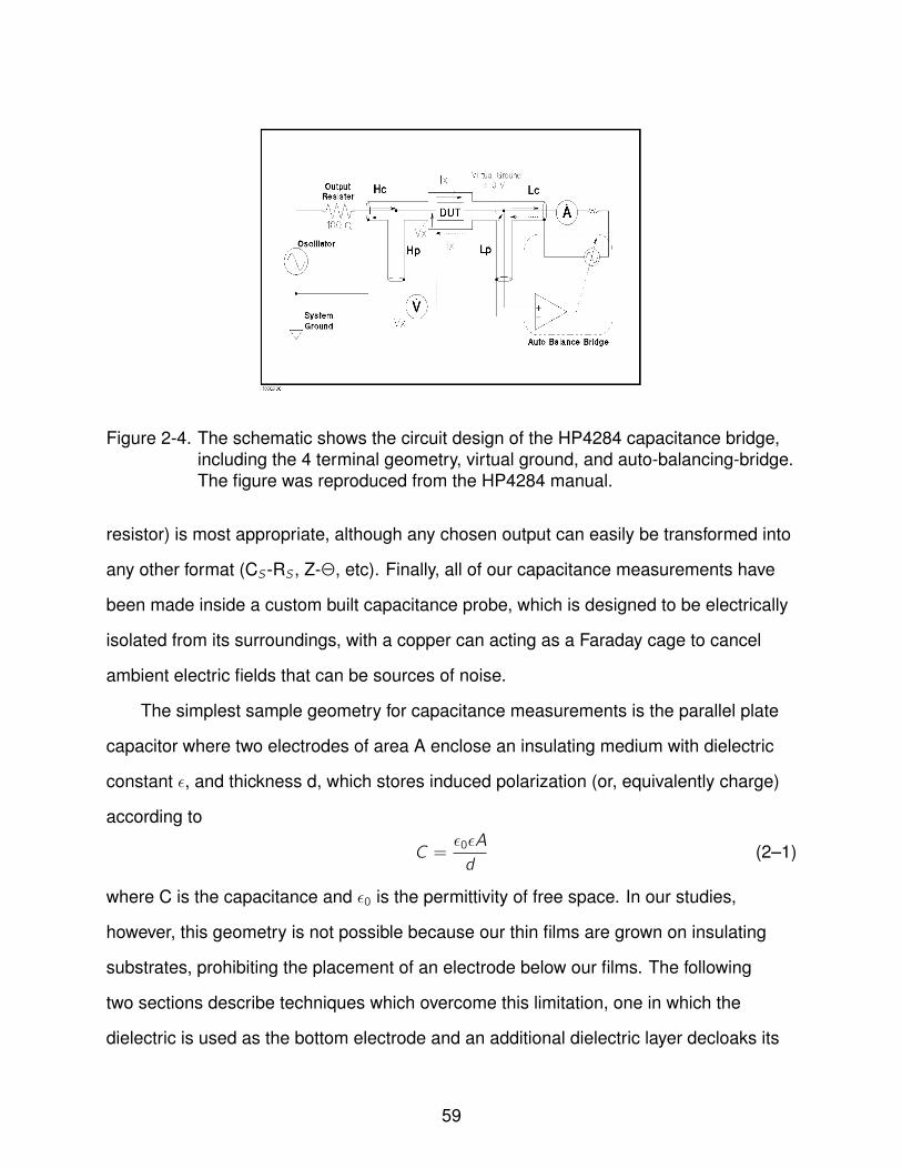
Figure 2-4. The schematic shows the circuit design of the HP4284 capacitance bridge,including the 4 terminal geometry, virtual ground, and auto-balancing-bridge.The figure was reproduced from the HP4284 manual.
resistor) is most appropriate, although any chosen output can easily be transformed into
any other format (CS-RS , Z-Θ, etc). Finally, all of our capacitance measurements have
been made inside a custom built capacitance probe, which is designed to be electrically
isolated from its surroundings, with a copper can acting as a Faraday cage to cancel
ambient electric fields that can be sources of noise.
The simplest sample geometry for capacitance measurements is the parallel plate
capacitor where two electrodes of area A enclose an insulating medium with dielectric
constant ε, and thickness d, which stores induced polarization (or, equivalently charge)
according to
C =ε0εA
d(2–1)
where C is the capacitance and ε0 is the permittivity of free space. In our studies,
however, this geometry is not possible because our thin films are grown on insulating
substrates, prohibiting the placement of an electrode below our films. The following
two sections describe techniques which overcome this limitation, one in which the
dielectric is used as the bottom electrode and an additional dielectric layer decloaks its
59
capacitance, and a second one in which a modified top interdigital electrode geometry is
used.
2.4.2 Dielectric Electrodes
A dielectric analysis technique was developed in Dr. Hebard’s lab (prior to this
thesis research) which demonstrated that it is possible to detect the dielectric response
of the bottom electrode in a tri-layer (metal-insulator-metal) parallel plate capacitor [18].
Analyzing the complex impedance of appropriate circuit models, it was shown that if
certain experimental constraints are met, the equipotential planes in the electrode will
be parallel to the electrode-dielectric layer interface, resulting in sensitivity to the c-axis
capacitance of the bottom electrode.
They began by modeling the entire structure as a resistance in series to a lossy and
leaky capacitor, where the series resistance is the a-b plane resistance of the LPCMO
film (see Fig 2-5 a)). The term lossy here refers to a complex capacitor (C ∗ = C1 − iC2)that dissipates energy from dipole reorientations, but does not pass dc current. Thus,
the addition of a shunting resistance in parallel results in a lossy, leaky capacitor that
does pass dc. In our structures the shunting resistance was found to be extremely large
R0 > 1010Ω, whereas at maximum RS ≈ 107Ω, meaning that 99.9% of a dc voltage is
applied across C ∗ and that RS can be ignored.
However, when the voltage is ac there are multiple current paths available (R0 and
R2 = 1/ωC2, see Fig. 2-5 b)). Since we are interested in the dielectric properties, we
choose our frequency range so that R2 << R0 ensuring the current passes through R2.
By measuring at frequencies above this lower bound we ensure that we are sensitive
to C ∗, but as frequency increases the voltage drop across RS (which is frequency
independent) will increase and eventually distort the capacitance measurements.
Analyzing the complex impedance of the circuit, however, provides a set of impedance
constraints that determine when the voltage drop across RS is negligble.
60

A) B)
C) D)
Figure 2-5. A) The circuit equivalent of the two-terminal measurement configurationwhere RS is the series resistance of the LPCMO sample and the parallelcombination of a complex (lossy) capacitor C ∗(ω) with a resistor R0represents the impedance of the LPCMO in series with the aluminum oxidecapacitor is shown. In the two-terminal configuration, the longitudinal voltagedrop across Rs cannot be distinguished from the perpendicular voltage dropacross the parallel combination of C ∗(ω) and R0. B) The decomposition ofC ∗(ω) = C1(ω) iC2(ω) into a parallel combination of C1(ω) and R2(ω) =1/ωC2(ω) is shown. C), The circuit equivalent for the capacitance CP(ω) andconductance 1/RP(ω) reported by the capacitance bridge is shown. D) TheMaxwell-Wagner circuit equivalent for the LPCMO impedance in series withthe Al/AlOx capacitor is shown. The LPCMO manganite film impedance isrepresented as a lossy capacitor C ∗M(ω) shunted by a resistor RM . There isno shunting resistor across CAlOx because the measured lower bound on R0is 1010, well above the highest impedance of the other circuit elements. Thefigure is reproduced from Ref. [18]
61

With the capacitance bridge set in parallel mode, the measured complex impedance
is reported in terms of a parallel capacitance, CP , and resistance, RP (see Fig. 2-5 c)).
Using simple circuit analysis it can be shown that the CP and RP of the model circuit can
be written in terms of the model circuit components as,
CP = C1(R22 (ω)
(R2(ω) + RS)2 + (ωRSR2(ω)C1(ω))2) (2–2)
RP =(R2(ω) + RS)
2 + (ωRSR2(ω)C1(ω))2
(R2(ω) + RS) + ω2RSR22 (ω)C21 (ω))
(2–3)
. If RS is small enough that,
RS << min 1
ωC1(ω),1
ωC2(ω),C2
ωC 21 (ω) (2–4)
then RP ≈ R2 and CP ≈ C1. The constraint can then be rewritten in terms of our
measurement parameters making it directly testable.
RS << min 1
ωCP(ω),1
ωC2(ω),C2
ωC 2P(ω). (2–5)
Once it has been determined that RS has not corrupted the capacitance
measurements, complex plane analysis can be used to ensure that the measured signal
is not a convolution of the electrode and the capping dielectric layer’s capacitances,
but that the measurement of each is separated into isolated regimes of the frequency
spectrum. The complex capacitance, C ∗, is now interpreted in terms of the classic
Maxwell-Wagner circuit, shown in Fig. 2-5 d). The Maxwell-Wagner circuit is commonly
used to account for the effects of contacts in dielectric measurements and is composed
of two leaky capacitors in series - here the manganite capacitance and the AlOx
capacitance. Fig. 2-6 b) shows a parametric plot of the complex impedance of a model
Maxwell-Wagner circuit with frequency the implicit variable. If CM << CAlOx then the
impedances of each capacitor will be isolated in separate frequency ranges as shown in
Fig. 2-6, and high-frequency measurements are guaranteed to be sensitive to only the
62

Figure 2-6. A Maxwell-Wagner circuit simulation is shown. This is a parametric plot ofthe complex imepedance (with frequency the implicit variable) of a simulatedMaxwell-Wagner circuit. Note the three time-scales, one characteristic foreach series component, and one marking the cross-over in the dominantresponse.
dielectric response of the electrode. Because the transverse voltage drop is known to be
negligible, this means the measurement is sensitive to the c-axis capacitance.
2.4.3 Interdigital Capacitance
Interdigital capacitance is a well established dielectric technique enabling
polarization measurements while only connecting to a single side of a dielectric. This
geometry has proved useful for a myriad applications including microwave integrated
devices, optical and surface acoustic wave devices, optically controlled microwave
devices, thin-film acoustic/electronic transducerss, chemical and biological sensors, and
finally dielectric studies on thin films. The geometry consists of interwoven electrode
”fingers” which create fringing fields that penetrate the dielectric and create equipotential
planes between the positive and negative electrodes, thereby creating an effective
capacitance (see Fig. 2-7). We use this technique to study thin film BMO, which is
grown on insulating substrates making the placement of a bottom electrode challenging,
63

A)
B)
Figure 2-7. A) A z-axis view of an interdigital electrode array is shown λ is the spacingbetween electrode fingers of the same voltage. B) An x-axis view of aninterdigical array is shown. The alternating voltage of the fingers results inequipotential planes separating them. Figure reproduced from [47]
and the transverse resistance of which is too large to utilize dielectric-electrode
analysis described in section 2.4.2. Our interdigital electrodes were fabricated using
photolithography and thermal evaporation.
A 3:1 mixture of Shipley 1813 and thinner was spin coated at 4000 rpm for 45
seconds, depositing a 1.5 µm photoresist polymer layer on our BMO samples. The
samples were then pre-baked at 115 C for 45 seconds. Next, the sample was
positioned underneath a photolithography mask with a pattern similar to that shown
in Fig. 2-7 using a Karl Suss MA-6 Contact Mask Aligner. Once aligned the portions
of the sample visible through mask were exposed to UV light for 14.5 seconds, and
subsequently dissolved in AZ300 MIF developer and rinsed in deionized water. Finally
the samples were post-baked at 115 C for 1.5 minutes to harden them in preparation for
further processing. At this point in the process the samples now have open areas in the
shape of the electrodes, which are separated by a “snake” of photoresist that weaves
in-between the electrode fingers.
64
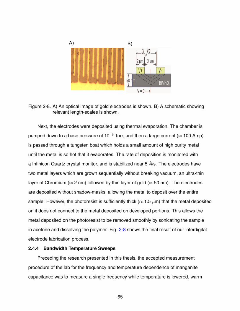
B)A)
Figure 2-8. A) An optical image of gold electrodes is shown. B) A schematic showingrelevant length-scales is shown.
Next, the electrodes were deposited using thermal evaporation. The chamber is
pumped down to a base pressure of 10−6 Torr, and then a large current (≈ 100 Amp)
is passed through a tungsten boat which holds a small amount of high purity metal
until the metal is so hot that it evaporates. The rate of deposition is monitored with
a Infinicon Quartz crystal monitor, and is stabilized near 5 A/s. The electrodes have
two metal layers which are grown sequentially without breaking vacuum, an ultra-thin
layer of Chromium (≈ 2 nm) followed by thin layer of gold (≈ 50 nm). The electrodes
are deposited without shadow-masks, allowing the metal to deposit over the entire
sample. However, the photoresist is sufficiently thick (≈ 1.5 µm) that the metal deposited
on it does not connect to the metal deposited on developed portions. This allows the
metal deposited on the photoresist to be removed smoothly by sonicating the sample
in acetone and dissolving the polymer. Fig. 2-8 shows the final result of our interdigital
electrode fabrication process.
2.4.4 Bandwidth Temperature Sweeps
Preceding the research presented in this thesis, the accepted measurement
procedure of the lab for the frequency and temperature dependence of manganite
capacitance was to measure a single frequency while temperature is lowered, warm
65
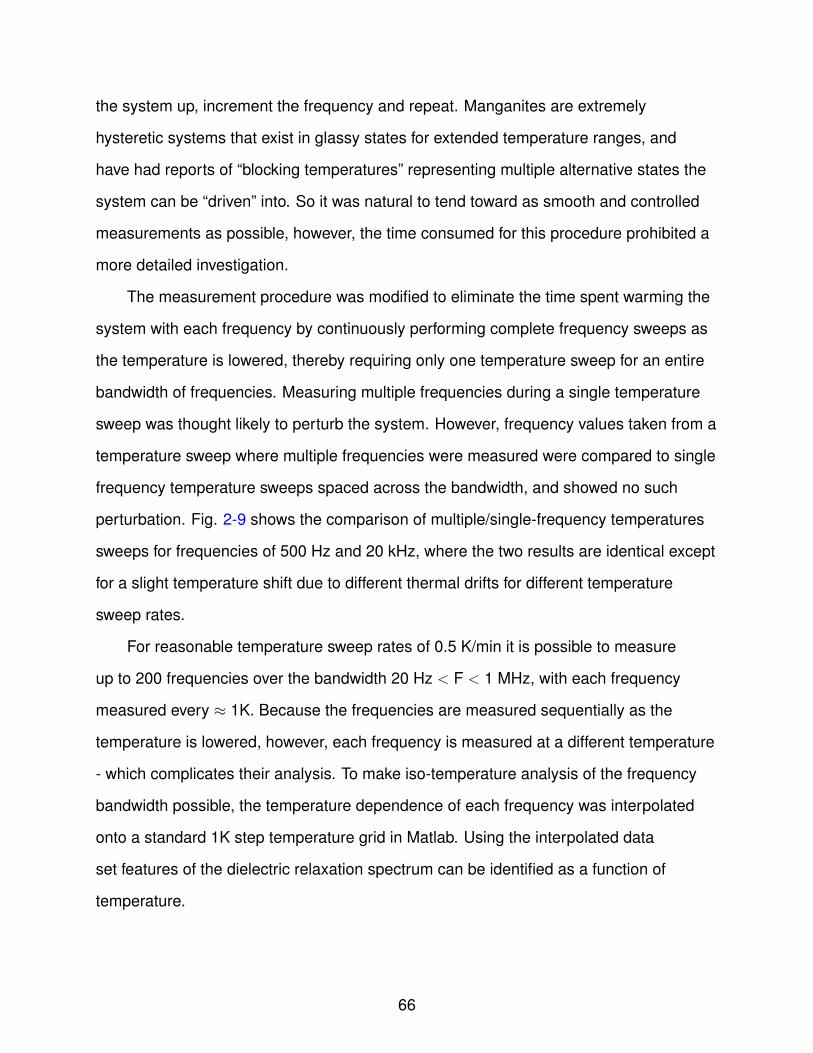
the system up, increment the frequency and repeat. Manganites are extremely
hysteretic systems that exist in glassy states for extended temperature ranges, and
have had reports of “blocking temperatures” representing multiple alternative states the
system can be “driven” into. So it was natural to tend toward as smooth and controlled
measurements as possible, however, the time consumed for this procedure prohibited a
more detailed investigation.
The measurement procedure was modified to eliminate the time spent warming the
system with each frequency by continuously performing complete frequency sweeps as
the temperature is lowered, thereby requiring only one temperature sweep for an entire
bandwidth of frequencies. Measuring multiple frequencies during a single temperature
sweep was thought likely to perturb the system. However, frequency values taken from a
temperature sweep where multiple frequencies were measured were compared to single
frequency temperature sweeps spaced across the bandwidth, and showed no such
perturbation. Fig. 2-9 shows the comparison of multiple/single-frequency temperatures
sweeps for frequencies of 500 Hz and 20 kHz, where the two results are identical except
for a slight temperature shift due to different thermal drifts for different temperature
sweep rates.
For reasonable temperature sweep rates of 0.5 K/min it is possible to measure
up to 200 frequencies over the bandwidth 20 Hz < F < 1 MHz, with each frequency
measured every ≈ 1K. Because the frequencies are measured sequentially as the
temperature is lowered, however, each frequency is measured at a different temperature
- which complicates their analysis. To make iso-temperature analysis of the frequency
bandwidth possible, the temperature dependence of each frequency was interpolated
onto a standard 1K step temperature grid in Matlab. Using the interpolated data
set features of the dielectric relaxation spectrum can be identified as a function of
temperature.
66
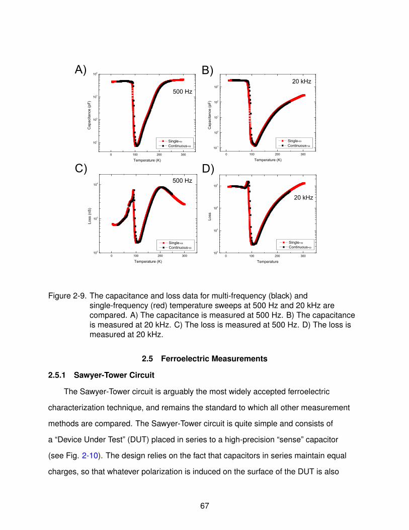
0 100 200 300102
103
104
105
Loss
Temperature
Single- Continuous-
20 kHz
0 100 200 300
101
102
103
104
Cap
acita
nce
(pF)
Temperature (K)
Single- Continuous-
500 Hz
0 100 200 300102
103
104
Loss
(nS
)
Temperature (K)
Single- Continuous-
500 Hz
0 100 200 300
10-1
100
101
102
103
Single- Continuous-
Cap
acita
nce
(pF)
Temperature (K)
20 kHzA) B)
C) D)
Figure 2-9. The capacitance and loss data for multi-frequency (black) andsingle-frequency (red) temperature sweeps at 500 Hz and 20 kHz arecompared. A) The capacitance is measured at 500 Hz. B) The capacitanceis measured at 20 kHz. C) The loss is measured at 500 Hz. D) The loss ismeasured at 20 kHz.
2.5 Ferroelectric Measurements
2.5.1 Sawyer-Tower Circuit
The Sawyer-Tower circuit is arguably the most widely accepted ferroelectric
characterization technique, and remains the standard to which all other measurement
methods are compared. The Sawyer-Tower circuit is quite simple and consists of
a “Device Under Test” (DUT) placed in series to a high-precision “sense” capacitor
(see Fig. 2-10). The design relies on the fact that capacitors in series maintain equal
charges, so that whatever polarization is induced on the surface of the DUT is also
67
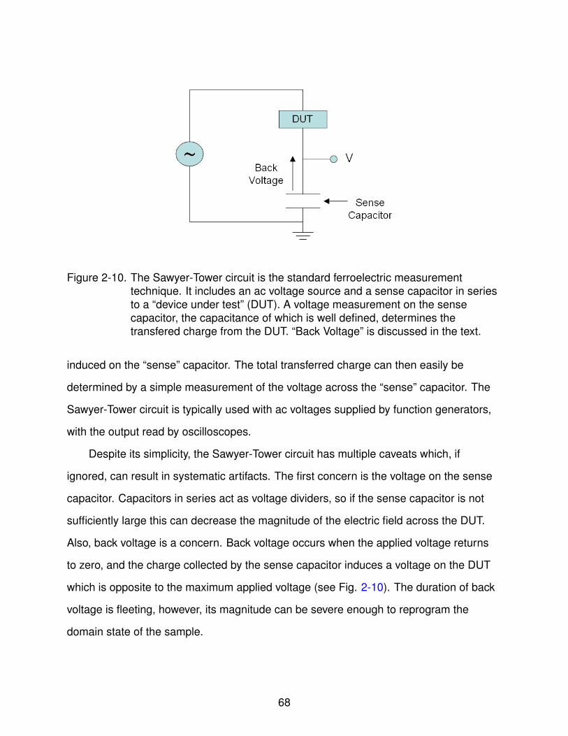
Figure 2-10. The Sawyer-Tower circuit is the standard ferroelectric measurementtechnique. It includes an ac voltage source and a sense capacitor in seriesto a “device under test” (DUT). A voltage measurement on the sensecapacitor, the capacitance of which is well defined, determines thetransfered charge from the DUT. “Back Voltage” is discussed in the text.
induced on the “sense” capacitor. The total transferred charge can then easily be
determined by a simple measurement of the voltage across the “sense” capacitor. The
Sawyer-Tower circuit is typically used with ac voltages supplied by function generators,
with the output read by oscilloscopes.
Despite its simplicity, the Sawyer-Tower circuit has multiple caveats which, if
ignored, can result in systematic artifacts. The first concern is the voltage on the sense
capacitor. Capacitors in series act as voltage dividers, so if the sense capacitor is not
sufficiently large this can decrease the magnitude of the electric field across the DUT.
Also, back voltage is a concern. Back voltage occurs when the applied voltage returns
to zero, and the charge collected by the sense capacitor induces a voltage on the DUT
which is opposite to the maximum applied voltage (see Fig. 2-10). The duration of back
voltage is fleeting, however, its magnitude can be severe enough to reprogram the
domain state of the sample.
68

The second concern when using the Sawyer-Tower circuit is that of parasitic
capacitance. The accuracy of the Sawyer-Tower circuit is tied directly to the known
precision of the sense capacitor, so parasitic capacitances in parallel can compromise
the confidence of the calculations of induced charge. Parasitic capacitances come from
multiple sources including measurement circuitry, and sample cables each of which can
add as much as 10pF.
The final and most important concern when using the Sawyer-Tower circuit is that it
provides no information about the origin of the charge induced on the sense capacitor.
The charge could be due to leakage in the DUT, to the capacitance of DUT, or to the
reversal of ferroelectric domains in the DUT. While the shape of hysteresis curves
can suggest which sources are responsible, ultimately the Sawyer-Tower circuit is not
equipped to discriminate the sources of charge contributions.
2.5.2 Precision LC: Ferroelectric Tester
The ferroelectric measurements in this thesis are made using a Radiant
Technologies Precision LC, Ferroelctric Tester. The Precision LC’s design is essentially
an evolution of the Sawyer-Tower circuit, with the addition of a virtual ground preceding
the sense capacitor (see 2-11). A virtual ground is a negative feedback system that
guarantees that a specific point in a circuit maintains a desired potential, in this case
V=0. The feedback is generated by connecting the specified location to the inverting
input and a ground to the non-inverting input of an op-amp. If the specified location
develops a positive (negative) potential, then the result of the inverting input is to create
a negative (positive) voltage at the output. Because this output is connected to the
specified location this inversion provides feedback that shifts the potential until the two
inputs are equal, and in this case grounded.
The addition of a virtual ground to the circuit design elegantly solves two of the
caveats described in the ”Sawyer-Tower Circuit” section above. By guaranteeing that
the potential just below the DUT is maintained at ground, the issue of back voltage is
69

0 2 4 6 8 100
2
4
6
8
10
Figure 2-11. Precision LC circuitry is reproduced from the Radiant manual.
completely circumvented. Similarly, parasitic capacitances are also greatly reduced
because the return path is always grounded, therefore both sides of the parasitic
capacitances are at ground and no charge can accumulate. Charge only accumulates
on the integrator, which is on the other side of the virtual ground.
2.5.3 Remanent Polarization
In ferroelectrics, the most important physical quantity is typically the remanent
polarization. The remanent polarization is composed of domains of spontaneous
dipoles, the orientations of which are dependent on the voltage history of the sample.
The Sawyer-Tower circuit and Precision LC are sensitive to the remanent polarization
because once a critical voltage (the coercive voltage) is reached the spontaneous
dipoles will flip and align themselves with the electric field. This results in a transfer of
charge which is detected by a voltage across the sense capacitor. This detection is
ambiguous, however, as it is difficult to definitively state the charge is due to domain
reversals and not an alternative source of charge such as resistive leakage or the
displacement current from capacitor charging. The total polarization measured in a
70

typical PE loop can be approximated to be composed as,
Ptot ≈ remanent + capacitance + diodes + resistors. (2–6)
The current explosion of interest in multiferroics has fallen victim to this subtlety on
many occasions, and this point was recently driven home sarcastically in a paper
entitled ”Ferroelectrics go bananas” where the author literally measured a banana to
show that its resistive leakage leads to polarization-vs-electric-field (PE) loops which
resembles those claiming to be ferroelectric in the multiferroic literature. Unequivocally
determining the presence of remanent polarization is therefore crucial for studying
ferroelectrics and identifying multiferroics. By implementing specific pulse sequences
and voltage waveforms the Precision LC is capable of resolving this issue, determining
the contributions of each component to the total transferred charge.
The equation for the total polarization (2–6) may be rewritten in terms of only two
components: remanent polarization, and non-remanent polarization,
Ptot ≈ remanent + non-remanent. (2–7)
The principle that allows these components to be resolved is that the remanent
polarization is sensitive to previously applied voltages, and the non-remanent
polarization is not. By applying presetting pulses that exceed the coercive voltage,
the orientation of the polarization of the ferroelectric domains, and thus their contribution
to hysteresis loops, can be controlled. Figure 2-12 shows two hysteresis waveforms
which utilize this principle. Presetting pulses align the ferroelectric domains along the
direction of the subsequent electric field (for both the positive and negative portions of
the hysteresis voltage waveform), guaranteeing that any charge transferred during the
hysteresis measurement cannot be from ferroelectric domain reversals - the domains
are already oriented along the field. Figure 2-12b illustrates the opposite scenario, in this
waveform presetting pulses align the domains anti-parallel to the following electric fields,
71

A)
B)
Figure 2-12. In the remanent polarization pulse sequence, presetting pulses (blue)precede hysteresis-loop voltage sections (red), guaranteeing either none A)or all B) of the ferroelectric dipoles are available to flip and contribute to themeasured transfer charge.
guaranteeing that all of the domains are available to flip during the hysteresis voltage
sweeps. The non-remanent polarization is the same in both hysteresis measurements,
however, only b) has contributions from ferroelectric domain reversals. Therefore,
subtracting the hysteresis loop of waveform a) from the hysteresis loop of waveform
b) results in a purely remanent hysteresis loop. This measurement procedure is used
extensively in the discussion of multiferroics in this thesis.
72

CHAPTER 3‘SOFT ELECTRONIC MATTER’ IN LPCMO
3.1 Introduction
This chapter will present strong experimental evidence for the existence of
‘electronically soft’ phases in mixed-valence manganites, providing important context
to the debate of the fundamental mechanisms driving phase separation/competition
in complex oxides. Measuring the frequency dependence of the complex
capacitance, we identify signatures of phase separation in the dielectric response of
(La1−yPry )1−xCaxMnO3 thin films, and present an analysis enabling the simultaneous
characterization of both dielectric phases, thereby enabling a spatial and temporal
description of the dynamic competition between these phases over a broad temperature
range. We find that the thermodynamic constraints imposed by detailed balance
strongly support the notion of an ‘electronically soft’ material, as we observe continuous
conversions between micron size dielectric phases with comparable free energies
competing on time scales that are long compared with electron-phonon scattering times.
Phase separation and phase competition are associated with many of the most
exotic material properties that complex oxides have to offer and are found ubiquitously
in high-temperature superconductors [48, 49], spinels [50], multiferroics [51, 52], and
mixed-valence manganites [16, 17]. Accordingly, understanding the fundamental
mechanisms of phase separation/competition is a strong priority for physicists, and
is necessary for the technological implementation of these next generation materials.
Importantly, the findings described in this chapter support a recent theory that predicted
‘electronically soft’ phases composed of ‘charge-density-waves’, challenging the static
disorder and strain based explanations of phase separation. This theory has broad
implications for complex oxides with coexisting and competing phases [53–55], however,
evidence for ‘electronically soft’ phases has yet to be provided.
73
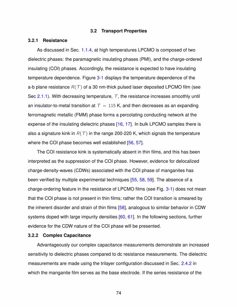
3.2 Transport Properties
3.2.1 Resistance
As discussed in Sec. 1.1.4, at high temperatures LPCMO is composed of two
dielectric phases: the paramagnetic insulating phases (PMI), and the charge-ordered
insulating (COI) phases. Accordingly, the resistance is expected to have insulating
temperature dependence. Figure 3-1 displays the temperature dependence of the
a-b plane resistance R(T ) of a 30 nm-thick pulsed laser deposited LPCMO film (see
Sec 2.1.1). With decreasing temperature, T , the resistance increases smoothly until
an insulator-to-metal transition at T = 115 K, and then decreases as an expanding
ferromagnetic metallic (FMM) phase forms a percolating conducting network at the
expense of the insulating dielectric phases [16, 17]. In bulk LPCMO samples there is
also a signature kink in R(T ) in the range 200-220 K, which signals the temperature
where the COI phase becomes well established [56, 57].
The COI resistance kink is systematically absent in thin films, and this has been
interpreted as the suppression of the COI phase. However, evidence for delocalized
charge-density-waves (CDWs) associated with the COI phase of manganites has
been verified by multiple experimental techniques [55, 58, 59]. The absence of a
charge-ordering feature in the resistance of LPCMO films (see Fig. 3-1) does not mean
that the COI phase is not present in thin films; rather the COI transition is smeared by
the inherent disorder and strain of thin films [58], analogous to similar behavior in CDW
systems doped with large impurity densities [60, 61]. In the following sections, further
evidence for the CDW nature of the COI phase will be presented.
3.2.2 Complex Capacitance
Advantageously our complex capacitance measurements demonstrate an increased
sensitivity to dielectric phases compared to dc resistance measurements. The dielectric
measurements are made using the trilayer configuration discussed in Sec. 2.4.2 in
which the manganite film serves as the base electrode. If the series resistance of the
74
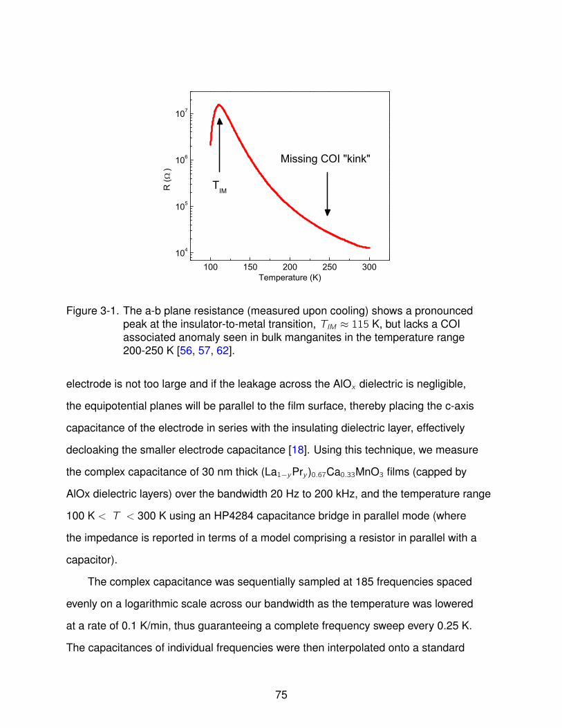
100 150 200 250 300104
105
106
107
R (
)
Temperature (K)
TIM
Missing COI "kink"
Figure 3-1. The a-b plane resistance (measured upon cooling) shows a pronouncedpeak at the insulator-to-metal transition, TIM ≈ 115 K, but lacks a COIassociated anomaly seen in bulk manganites in the temperature range200-250 K [56, 57, 62].
electrode is not too large and if the leakage across the AlOx dielectric is negligible,
the equipotential planes will be parallel to the film surface, thereby placing the c-axis
capacitance of the electrode in series with the insulating dielectric layer, effectively
decloaking the smaller electrode capacitance [18]. Using this technique, we measure
the complex capacitance of 30 nm thick (La1−yPry )0.67Ca0.33MnO3 films (capped by
AlOx dielectric layers) over the bandwidth 20 Hz to 200 kHz, and the temperature range
100 K < T < 300 K using an HP4284 capacitance bridge in parallel mode (where
the impedance is reported in terms of a model comprising a resistor in parallel with a
capacitor).
The complex capacitance was sequentially sampled at 185 frequencies spaced
evenly on a logarithmic scale across our bandwidth as the temperature was lowered
at a rate of 0.1 K/min, thus guaranteeing a complete frequency sweep every 0.25 K.
The capacitances of individual frequencies were then interpolated onto a standard
75
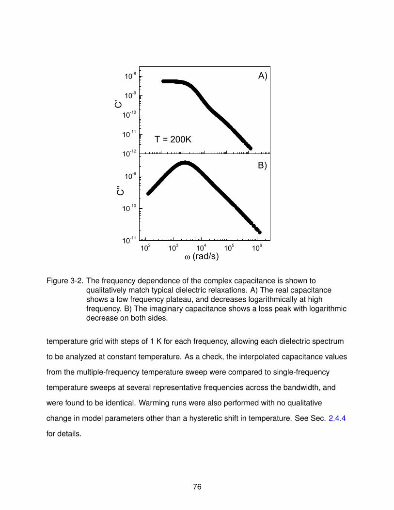
102 103 104 105 10610-11
10-10
10-9
(rad/s)
C''
B)10-12
10-11
10-10
10-9
10-8
A)
C'
T = 200K
Figure 3-2. The frequency dependence of the complex capacitance is shown toqualitatively match typical dielectric relaxations. A) The real capacitanceshows a low frequency plateau, and decreases logarithmically at highfrequency. B) The imaginary capacitance shows a loss peak with logarithmicdecrease on both sides.
temperature grid with steps of 1 K for each frequency, allowing each dielectric spectrum
to be analyzed at constant temperature. As a check, the interpolated capacitance values
from the multiple-frequency temperature sweep were compared to single-frequency
temperature sweeps at several representative frequencies across the bandwidth, and
were found to be identical. Warming runs were also performed with no qualitative
change in model parameters other than a hysteretic shift in temperature. See Sec. 2.4.4
for details.
76

10-12 10-11 10-10 10-9 10-810-11
10-10
10-9
10-8
C'' (
F)
C' (F)
Figure 3-3. In the Cole-Cole representation of the complex capacitance, the imaginarycapacitance is plotted parametrically as a function of the real capacitancewith the measuring frequency, ω, varied as the implicit parameter.
At first glance our complex capacitance data (where C = C ′ − iC ′′) displays all of
the qualitative features of a dielectric relaxation (see 3-2): in the real component there
is a low frequency plateau with minimal dispersion, followed by a logarithmic decrease
at high frequencies, while the imaginary component displays a clear loss peak with
logarithmic decreases on either side. However, when the dielectric data is analyzed
quantitatively, it is not consistent with dielectric theories describing single phases.
A common convention for analyzing complex capacitance data utilizes the
Cole-Cole representation. In Cole-Cole plots, the imaginary capacitance is plotted
parametrically as a function of the real capacitance, with the measurement frequency
varied as the implicit parameter, allowing for a simultaneous analysis of both
components. Figure 3-3 shows a Cole-Cole plot of our complex capacitance data
at 200 K. To compare our data to standard dielectric theories, we further calculate
the logarithmic parametric slope, (∂(ln C ′′)/∂ω)/(∂(ln C ′)/∂ω), at each point of Fig.
3-3. Figure 3-4 shows the calculated logarithimc parametric slope as a function of
77

103 104 105 1060.0
0.4
0.8
1.2
C'/C
''(C
''/C
')
UDR
Cole-Cole
(rad/s)
T = 200K
Figure 3-4. The logarithmic parametric-slope, (C ′/C ′′)(∂C ′′/∂C ′) (green), is shown todiffer from the Cole-Cole [64] dielectric response and ‘Universal’ dielectricresponse [63].
frequency, compared to a Cole-Cole dielectric response function, and ‘Universal’
dielectric response (UDR). Cole-Cole dielectric functions have the form:
ε(ω) = ε∞ +ε0 − εinf
1 + (iωτ)1−α, (3–1)
where τ is a characteristic relaxation time-scale, α is a time-scale broadening, and
the difference between the zero frequency and infinite frequency dielectric constants,
ε0 − εinf , determines the amplitude of the relaxation. UDR refers to the ubiquitous trend
in dielectrics that at high frequency both components share a fractional power-law
dependence in frequency: ∝ ωn−1 [63]. UDR results in a logarithmic parametric slope of
1, as both components are changing with frequency at the same rate.
As seen in Fig. 3-4, our data are inconsistent with both dielectric theories (only
slopes greater than zero are shown for clarity). The Cole-Cole response increases
monotonically toward the UDR slope of 1, while our data displays a high-frequency
non-monotonic anamoly, and then appears to saturate for an extended bandwidth.
78
103 104 105 1060.0
0.4
0.8
1.2
C'/C
''(C
''/C
')
(rad/s)
PMI
COI
Figure 3-5. The logarithmic parametric-slope, (C ′/C ′′)(∂C ′′/∂C ′) (green), is shown todiffer from the Cole-Cole [64] dielectric response, providing a signature ofmultiple phases.
The following sections will demonstrate that both of these features are the result of the
first order competition between the PMI and COI dielectric phases [65]. Furthermore,
characterizing the temperature dependence of their competition reveals a highly
correlated collective transport mode of the COI phase domains, similar to the ‘coherent
creep’ preceding ‘sliding’ in CDW systems [66].
3.3 Competing Dielectric Phases
It appears that there are two dominant time-scales in the logarithmic parametric
slope of the dielectric response. The first time-scale is centered at the loss peak, where
the logarithmic parametric slope is zero (locally C ′′ does not change with frequency
there), and the second time-scale is centered at the high-frequency non-monotonic
anomaly. Knowing that there are two competing dielectric phases at high temperatures
in bulk samples motivated a simple hypothesis: one dielectric phase’s relaxation is
centered at the loss peak, and the other dielectric phase’s relaxation is centered at the
high frequency anomaly. This hypothesis is illustrated in Fig. 3-5.
79

3.3.1 Modeling
Figure 3-6 displays a circuit model that was developed which takes this hypothesis
into account. The circuit is composed of three parallel components all in series to
fractional areas of the AlOx dielectric layer: aCOI , aPMI , and aR (the fractional area of the
FMM phase, which acts as a resistive short at low temperatures), with the constraint∑ai = 1. The series resistance is an artifact of measuring the dielectric response
of an electrode in a MIM structure, and is discussed in detail in Sec. 2.4.2. Placing
the capacitances of each phase in parallel requires that the domains of each phase
span the film thickness, thus obviating a series configuration. Our film thickness of
30 nm, however, satisfies this requirement for the phase domains of manganites, the
length-scales of which are known to be on the order of microns [17]. Above TIM , aR ≈ 0,and the circuit is dominated by CPMI and CCOI in our frequency range, so that the
total complex dielectric response may be approximated by the superimposition of two
Cole-Cole dielectric functions,
C ∝ ε(ω) = ε∞ +APMI
1 + (iωτPMI )1−α+
ACOI1 + (iωτCOI )1−β
, (3–2)
where the amplitudes Ai are the product of the fractional area ai and dielectric constant
εi of each phase, i.e., Ai = aiεi , and ε∞ is the sum of the infinite frequency response of
each dielectric phase.
We model our complex capacitance data with Eq. 3–2 at fixed temperatures in 1 K
steps between 100 K and 350 K by varying ω = 2πf over 185 frequencies. The fits are
produced by simultaneously minimizing the difference between the measured complex
capacitance and both the real and imaginary parts of Eq. (2). In the low-frequency limit,
ε(0) ≈ APMI + ACOI , allowing a fitting variable to be eliminated by reparameterizing the
dielectric amplitudes in terms of their ratio, ramp = ACOI/APMI , and the measured ε(0),
i.e., APMI = ε(0)/(1 + ramp),and ACOI = ramp ε(0)/(1 + ramp). As τPMI is determined from
80

aCOIaPMI
RmetRS
CPMI & COI
CAlOx
~
aR
Figure 3-6. In our circuit model, three parallel components, CPMI , CCOI , and Rmet , are inseries to fractional areas (aPMI , aCOI , and aR respectively) of the AlOx layer.Above the insulator to metal transition temperature, TIM , aR ≈ 0.
the loss peak frequency (see Fig. 3-7), five free variables are determined by the fits: ε∞,
ramp, α, β, and τCOI .
Figure 3-7 shows a typical fit to Eq. 3–2 (green curve) where the average relative
error is less than 10−3 for each temperature. Also shown are the individual relaxations
of each phase, the low frequency PMI phase (red) and the high frequency COI phase
(blue) (their identifications are discussed below). Importantly, Fig. 3-7 explains the
high-frequency non-monotonic anomaly in the logarithmic parametric slope. At low
frequencies, the PMI phase dominates both channels, and at high frequencies the COI
dominates in the real channel, but not the imaginary channel. This mixing of relaxation
components at high frequencies results in the logarithmic parametric-slope behaviour
seen in Figs. 3-4 and 3-5, and thus are a signature of phase separation between two
separate and readily identifiable dielectrics.
3.3.2 Temperature Dependence of Model Parameters
The temperature dependence of the model parameters provides a wealth of
physical knowledge, allowing us to identify the individual dielectric phases and
determine the microscopic mechanisms that manifest their material properties.
Dielectric broadening provides a measure of the correlations among relaxors, and
81
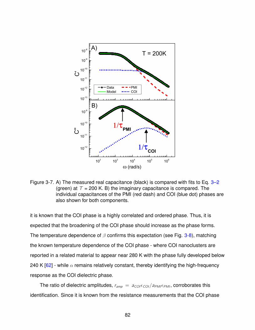
102 103 104 105 106
10-12
10-11
10-10
10-9
COI
PMI
(rad/s)
C''
B)10-13
10-12
10-11
10-10
10-9
10-8
A)
Data PMI Model COI
C'
T = 200K
Figure 3-7. A) The measured real capacitance (black) is compared with fits to Eq. 3–2(green) at T = 200 K. B) the imaginary capacitance is compared. Theindividual capacitances of the PMI (red dash) and COI (blue dot) phases arealso shown for both components.
it is known that the COI phase is a highly correlated and ordered phase. Thus, it is
expected that the broadening of the COI phase should increase as the phase forms.
The temperature dependence of β confirms this expectation (see Fig. 3-8), matching
the known temperature dependence of the COI phase - where COI nanoclusters are
reported in a related material to appear near 280 K with the phase fully developed below
240 K [62] - while α remains relatively constant, thereby identifying the high-frequency
response as the COI dielectric phase.
The ratio of dielectric amplitudes, ramp = aCOI εCOI/aPMI εPMI , corroborates this
identification. Since it is known from the resistance measurements that the COI phase
82
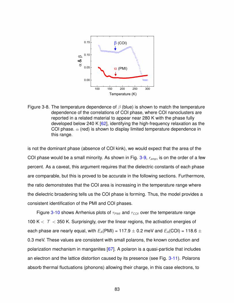
100 150 200 250 300
0.00
0.05
0.10
0.15 (COI)
Temperature (K)
&
(PMI)
Figure 3-8. The temperature dependence of β (blue) is shown to match the temperaturedependence of the correlations of COI phase, where COI nanoclusters arereported in a related material to appear near 280 K with the phase fullydeveloped below 240 K [62], identifying the high-frequency relaxation as theCOI phase. α (red) is shown to display limited temperature dependence inthis range.
is not the dominant phase (absence of COI kink), we would expect that the area of the
COI phase would be a small minority. As shown in Fig. 3-9, ramp, is on the order of a few
percent. As a caveat, this argument requires that the dielectric constants of each phase
are comparable, but this is proved to be accurate in the following sections. Furthermore,
the ratio demonstrates that the COI area is increasing in the temperature range where
the dielectric broadening tells us the COI phase is forming. Thus, the model provides a
consistent identification of the PMI and COI phases.
Figure 3-10 shows Arrhenius plots of τPMI and τCOI over the temperature range
100 K < T < 350 K. Surprisingly, over the linear regions, the activation energies of
each phase are nearly equal, with EA(PMI) = 117.9 ± 0.2 meV and EA(COI) = 118.6 ±0.3 meV. These values are consistent with small polarons, the known conduction and
polarization mechanism in manganites [67]. A polaron is a quasi-particle that includes
an electron and the lattice distortion caused by its presence (see Fig. 3-11). Polarons
absorb thermal fluctuations (phonons) allowing their charge, in this case electrons, to
83

100 150 200 250 300 3500.0000
0.0125
0.0250
Temperature (K)
r amp
Figure 3-9. The temperature dependence of ramp is shown to match the temperaturedependence of the COI phase, where COI nanoclusters are reported in arelated material to appear near 280 K with the phase fully developed below240 K [62], and identifying the high-frequency relaxation as the COI phase -consistent with the dielectric broadening data (β).
2 4 6 8 10
10-6
10-5
10-4
10-3
10-2
PMI
COI
1000/T (K-1)
PM
I&
CO
I
Figure 3-10. The Arrhenius plots are shown for τCOI and τPMI , with EA ≈ 118 meV in thelinear region for both dielectric phases, which identifies the polarizationmechanism as small polarons. The nearly identical EA’s suggest thephases share a single energy barrier.
hop to new spatial locations, where the local lattice site subsequently relaxes to the
(lower energy) distorted state. In manganites, this process is adiabatic where electrons
hop quickly and the lattice relaxes slowly around the relocated electron with a time-scale
at least as long as the electron hopping time-scale [67].
84

Figure 3-11. A polaron is a quasi-particle that includes an electron and the surrounding“cloud” of lattice distortions induced by its presence.
3.4 ‘Soft Electronic Matter’
3.4.1 Polarons and Detailed Balance
The strikingly similar activation energies of the two phases suggests the relaxations
are coupled, possibly sharing a common energy barrier. Crossing this energy barrier
would result in the two phases converting into each other. In our system, however,
each dielectric also polarizes independently without converting into the other phase.
Therefore, the phases would have to be connected through a common excited state
from which relaxations can occur to either phase. This common state is consistent
with adiabatic polaron hopping in manganites [67], where the lattice relaxes slowly in
response to fast electronic hopping.
We model this process in our samples by the three state system shown in Fig. 3-12.
The electrons of the polarons of both dielectric phases absorb thermal fluctuations that
activate them over their hopping barriers to an equivalent “excited” state: a relocated
electron surrounded by a lattice site that has yet to relax. The new lattice site has some
initial distortion (either PMI or COI), but as it accommodates the new electron it can
transform/relax into distortions that correspond to either dielectric phase. The electronic
hopping happens at characteristic rates which we measure directly from loss peak
positions in the complex capacitance (γPMI = 1/τPMI , and γCOI = 1/τCOI ). The lattice site
relaxation, however, occurs at unknown rates, γE and γ′E , for the PMI and COI phases
85
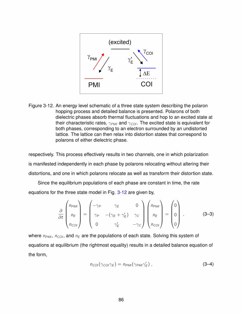
COI
PMI
E
E
COI
PMI
(excited)
'
Figure 3-12. An energy level schematic of a three state system describing the polaronhopping process and detailed balance is presented. Polarons of bothdielectric phases absorb thermal fluctuations and hop to an excited state attheir characteristic rates, γPMI and γCOI . The excited state is equivalent forboth phases, corresponding to an electron surrounded by an undistortedlattice. The lattice can then relax into distortion states that correspond topolarons of either dielectric phase.
respectively. This process effectively results in two channels, one in which polarization
is manifested independently in each phase by polarons relocating without altering their
distortions, and one in which polarons relocate as well as transform their distortion state.
Since the equilibrium populations of each phase are constant in time, the rate
equations for the three state model in Fig. 3-12 are given by,
∂
∂t
nPMI
nE
nCOI
=
−γP γE 0
γP −(γE + γ′E) γC
0 γ′E −γC
nPMI
nE
nCOI
=
0
0
0
, (3–3)
where nPMI , nCOI , and nE are the populations of each state. Solving this system of
equations at equilibrium (the rightmost equality) results in a detailed balance equation of
the form,
nCOI (γCOIγE) = nPMI (γPMIγ′E) , (3–4)
86
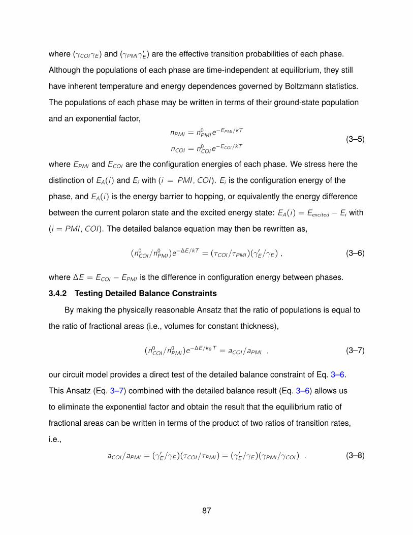
where (γCOIγE ) and (γPMIγ′E ) are the effective transition probabilities of each phase.
Although the populations of each phase are time-independent at equilibrium, they still
have inherent temperature and energy dependences governed by Boltzmann statistics.
The populations of each phase may be written in terms of their ground-state population
and an exponential factor,
nPMI = n0PMIe
−EPMI /kT
nCOI = n0COIe
−ECOI /kT(3–5)
where EPMI and ECOI are the configuration energies of each phase. We stress here the
distinction of EA(i) and Ei with (i = PMI ,COI ). Ei is the configuration energy of the
phase, and EA(i) is the energy barrier to hopping, or equivalently the energy difference
between the current polaron state and the excited energy state: EA(i) = Eexcited − Ei with
(i = PMI ,COI ). The detailed balance equation may then be rewritten as,
(n0COI/n0PMI )e
−∆E/kT = (τCOI/τPMI )(γ′E/γE) , (3–6)
where ∆E = ECOI − EPMI is the difference in configuration energy between phases.
3.4.2 Testing Detailed Balance Constraints
By making the physically reasonable Ansatz that the ratio of populations is equal to
the ratio of fractional areas (i.e., volumes for constant thickness),
(n0COI/n0PMI )e
−∆E/kBT = aCOI/aPMI , (3–7)
our circuit model provides a direct test of the detailed balance constraint of Eq. 3–6.
This Ansatz (Eq. 3–7) combined with the detailed balance result (Eq. 3–6) allows us
to eliminate the exponential factor and obtain the result that the equilibrium ratio of
fractional areas can be written in terms of the product of two ratios of transition rates,
i.e.,
aCOI/aPMI = (γ′E/γE)(τCOI/τPMI ) = (γ
′E/γE)(γPMI/γCOI ) . (3–8)
87

100 150 200 250 300 3500.000
0.025
0.050
0.075 r ramp
Temperature (K)
r amp &
r
Figure 3-13. The temperature dependence of ramp is shown to mirror that of rτ intemperature (with a constant offset factor), confirming our use of thedetailed balance equation.
We are able to verify this equation constrains our system because our model
determines the variables on either side to within a constant factor: rτ =τCOI/τPMI and
ramp = (aCOI/aPMI )(εCOI/εPMI ). Since detailed balance does in fact constrain our system,
then the independently determined ratios should have a constant offset factor over the
measured temperature range of, rτ/ramp = (εPMI/εCOI ) (assuming that γ′E/γE ≈ 1,which is discussed below). Figure 3-13 shows the temperature dependence of the
independently determined ratios, rτ and ramp. The two ratios follow a similar trend with a
ratio of ratios,
rτ/ramp = (τCOI/τPMI )(aPMI/aCOI )(εPMI/εCOI ) ≈ 2.4 (3–9)
which is constant within ±10% in the ranges 100 < T < 250 and 270 < T < 350,
with a small deviation near 260K which we ascribe to a modification to the ratio γE/γ′E
caused by the increase of correlations in the COI phase. Therefore, the temperature
dependence of the ratios differs only by a constant factor, thus confirming that detailed
balance constrains our system.
The combination of Eq. 3–6 and Eq. 3–7 together with the result that γ′E/γE ≈ 1leads to the relation aCOIγCOI ≈ aPMIγPMI which with the normalization, aCOI + aPMI = 1,
88
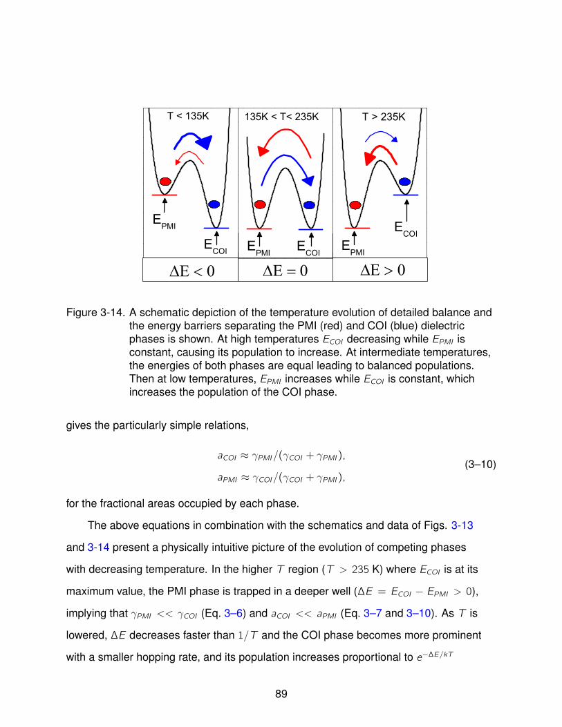
ECOI
T < 135K
ECOIEPMI
135K < T< 235K
ECOIEPMI
EPMI
T > 235K
Figure 3-14. A schematic depiction of the temperature evolution of detailed balance andthe energy barriers separating the PMI (red) and COI (blue) dielectricphases is shown. At high temperatures ECOI decreasing while EPMI isconstant, causing its population to increase. At intermediate temperatures,the energies of both phases are equal leading to balanced populations.Then at low temperatures, EPMI increases while ECOI is constant, whichincreases the population of the COI phase.
gives the particularly simple relations,
aCOI ≈ γPMI/(γCOI + γPMI ),
aPMI ≈ γCOI/(γCOI + γPMI ),(3–10)
for the fractional areas occupied by each phase.
The above equations in combination with the schematics and data of Figs. 3-13
and 3-14 present a physically intuitive picture of the evolution of competing phases
with decreasing temperature. In the higher T region (T > 235 K) where ECOI is at its
maximum value, the PMI phase is trapped in a deeper well (∆E = ECOI − EPMI > 0),
implying that γPMI << γCOI (Eq. 3–6) and aCOI << aPMI (Eq. 3–7 and 3–10). As T is
lowered, ∆E decreases faster than 1/T and the COI phase becomes more prominent
with a smaller hopping rate, and its population increases proportional to e−∆E/kT
89

(polarons remain in the state longer because of a deeper potential well). In this limit,
Eq. 3–10 shows aCOI ≈ γPMI/γCOI and aPMI ≈ 1 − γPMI/γCOI , confirming that the
fractional area occupied by the COI phase is substantially smaller than that of the
PMI phase. Then at intermediate temperatures, the two phases are at equal energies
(∆E = 0) over the surprisingly large temperature range of ∼ 100 K, making their
populations temperature independent. Within this region the energy barrier to escape
to the excited state is the same for each phase (118 meV) (Fig. 3-10. Finally, at low
temperatures the PMI phase destabilizes and ∆E becomes negative as EPMI increases
relative to ECOI . As a result the COI’s population increases proportional to e−∆E/kT as
seen in Fig. 3-13.
3.4.3 Lattice Relaxation Rates
Thus far, we have assumed that the ratio of relaxation rates from the excited state
was constant in temperature, and approximately equal to 1. In this section we will
discuss both of these claims. We gain additional insight into the lattice relaxation rates
by substituting Eq. 3–8 into Eq. 3–9 to obtain the result,
εPMI/εCOI = 2.4(γ′E/γE) . (3–11)
The implication of this result becomes apparent by recalling that in our modeling of
the total dielectric response as a superposition of two Cole-Cole dielectric functions
(Eq.3–2), we assumed the dielectric constants εi of the COI and PMI phases to be
temperature independent with all of the temperature dependence in the numerators
of the respective dielectric functions subsumed into the fractional areas ai = Ai/εi .
Accordingly, Eq. 3–11 then tells us that the ratio of lattice relaxation rates γ′E/γE is a
temperature-independent constant which for simplicity we assume is unity (discussed
further below). With this choice equations 3–7 and 3–8 can be combined to give
(n0COI/n0PMI )e
−∆E/kT = aCOI/aPMI = (τCOI/τPMI ) = (γPMI/γCOI ) , (3–12)
90

30 60 90 120 1500
15
30
45
Film Thickness (nm)
PM
I &
CO
I PMI COI
Figure 3-15. The dielectric constants, calculated from the dielectric amplitudes andareas of each phase, εi = Ai/ai , are shown to saturate near their bulkvalues once substrate strain is relaxed. The agreement with bulk datavalidates the areas calculated assuming equal lattice relaxation rates,γE ≈ γ′E .
hence confirming that rτ = τCOI/τPMI does, in fact, represent the ratio of areas.
Knowledge of the ratio of fractional areas aCOI/aPMI and the ratio of dielectric
amplitudes ACOI/APMI together with the respective constraining normalizations, aCOI +
aPMI = 1 and ACOI + APMI = ε(0), allow an experimental determination of the respective
dielectric constants εCOI = ACOI/aCOI and εPMI = APMI/aPMI . Figure 3-15 shows the
dielectric constants determined in this manner for four films with thickness ranging from
30 nm to 150 nm. The dielectric constants of each phase increase and saturate near
their known bulk values [68–70] as the substrate strain relaxes. In manganites grown
on NGO, the film is relaxed at a thickness of d ≈ 100 nm [15, 18] in agreement with the
saturation of the data in the figure. The agreement of the data with these expectations
tends to validate our assumption that γ′E/γE ≈ 1.3.4.4 Charge Density Waves
Interestingly, our data also present strong evidence for the existence of
charge-density waves (CDWs) in LPCMO, describing a collective and delocalized
91

10-6 10-5 10-4 10-3 10-2
0.0
0.5
1.0
(s)
G(
Figure 3-16. The normalized distributions of hopping-rate time-scales are shown to benarrow for both phases, suggesting temporally coherent hopping (PMIdotted red, and COI solid blue).
propagation of the charge-density distribution of the COI phase. The constraints of the
parallel model require that the hopping mechanism is correlated over sufficiently long
length scales that regions equal to at least the film thickness hop together collectively,
so that as the phases convert the entire phase boundaries progress simultaneously in a
‘creep’ like manner. ‘Creep’ is typically a random phenomenon, however, transforming
our dielectric broadening to a distribution of time-scales [71] (shown in the inset of
Fig. 4) we find a narrow distribution of hopping rates suggesting an ordered process
similar to the ‘temporally coherent creep’ found in the CDW system NbSe3 [66].
The exact nature of the order is ambiguous, with two likely scenarios. The first
possibility is the coherent propagation of phase domains, where as the phase boundary
‘creeps’ forward the regions behind synchronously hop, guaranteeing the continuity of
the phase. This scenario is depicted in the schematic of Fig. 3-17, where the boundaries
of the Mn3+/Mn4+ charge ordered phase (blue) coherently propagate with successive
phase boundary hops/creeping, supplanting and converting into the charge-disordered
paramagnetic insulating phase (red). The second scenario is a ‘breathing’ mode in
which the area of different phase domains cooperatively increase and decrease at a
characteristic frequency (with total area conserved). Both scenarios demonstrate the
92
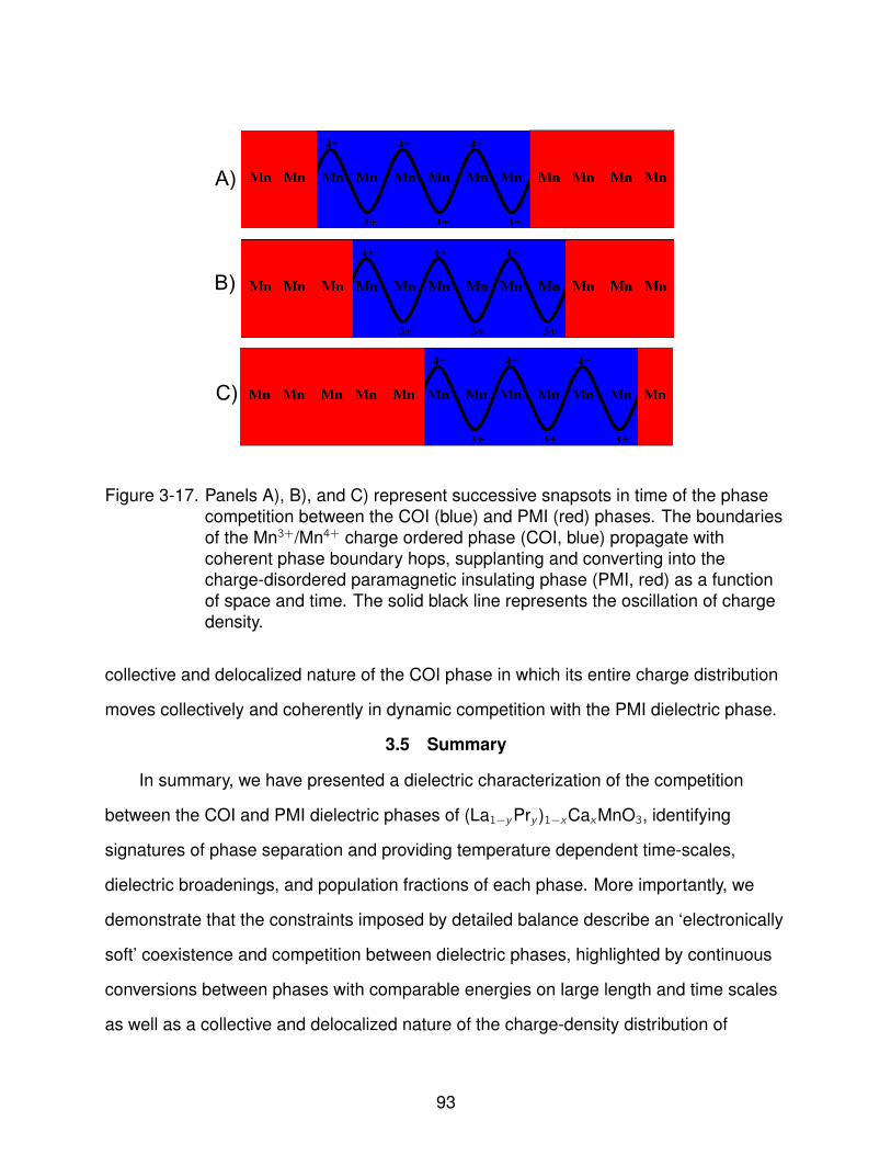
C)
B)
A)
Figure 3-17. Panels A), B), and C) represent successive snapsots in time of the phasecompetition between the COI (blue) and PMI (red) phases. The boundariesof the Mn3+/Mn4+ charge ordered phase (COI, blue) propagate withcoherent phase boundary hops, supplanting and converting into thecharge-disordered paramagnetic insulating phase (PMI, red) as a functionof space and time. The solid black line represents the oscillation of chargedensity.
collective and delocalized nature of the COI phase in which its entire charge distribution
moves collectively and coherently in dynamic competition with the PMI dielectric phase.
3.5 Summary
In summary, we have presented a dielectric characterization of the competition
between the COI and PMI dielectric phases of (La1−yPry )1−xCaxMnO3, identifying
signatures of phase separation and providing temperature dependent time-scales,
dielectric broadenings, and population fractions of each phase. More importantly, we
demonstrate that the constraints imposed by detailed balance describe an ‘electronically
soft’ coexistence and competition between dielectric phases, highlighted by continuous
conversions between phases with comparable energies on large length and time scales
as well as a collective and delocalized nature of the charge-density distribution of
93

the COI phase. Our findings provide important context concerning the fundamental
mechanisms driving phase separation, and strongly support the ‘electronically soft’,
delocalized and ordered thermodynamic phase interpretation (Ref. [72]) over the
disorder and strain based explanations which result in static phases.
94
CHAPTER 4STRAIN MEDIATED MAGNETOELECTRIC COUPLING IN (LA1−YPRY )1−XCAXMNO3
4.1 Introduction
Magnetoelectric (ME) coupling, the induction of electric (magnetic) polarization
by external magnetic (electric) fields, has recently become one of the most active
research topics due to both its complex physical origins and its potential technological
applications [22, 33, 42, 43]. Theoretically, ME coupling is typically described using
Ginzburg-Landau theory, where a free energy analysis provides a unified temperature
and field dependence of the thermodynamics and stability of the constituent electronic
phases. The free energy description also provides an infrastructure for testing
specific microscopic coupling mechanisms, and multiple mechanisms have been
shown to produce ME coupling: single ion anisotropy, symmetric and antisymmetric
superexchange, dipolar effects, Zeeman energy, and etc [73]. However, these couplings
are found to be systematically small [41].
Experimentally, large magnetoelectric coupling has been achieved in composites by
combining piezoelectric and magnetostrictive materials which couple through strain. The
coupling in composites can be multiple orders of magnitude larger than in single phase
materials, establishing strain coupling as the most powerful known magnetoelectric
mechanism and sparking a revival in magnetoelectric research [41, 74]. However, the
theoretical description of the large composite coupling has provided little insight into
the thermodynamics or microscopic magnetoelectric mechanisms, as it is estimated by
the simple phenomenological multiplication of bulk properties and is limited strictly to
the interfaces [41, 75]. Outside of composites, only indirect evidence of strain-mediated
magnetoelectric coupling has been demonstrated. For example, anomalies in the
dielectric constant have been shown to accompany structural transitions resulting from
antiferrodistortion at magnetic ordering temperatures [76].
95
In this chapter we present the first successful strain-based microscopic modeling
of magnetoelectric coupling data in single phases. Measuring the frequency
dependence of the complex capacitance, we show that the dielectric phases of thin film
(La1−xPrx )1−yCayMnO3 - paramagnetic insulating (PMI) and charge-ordered insulating
(COI) - each display two distinct magnetoelectric couplings: magnetic field tuning of both
the dielectric constants and activation energies. Using electric, magnetic, and elastic
terms in a free-energy expansion, we correctly predict the power and sign of magnetic
field induced modifications of the dielectric constant of each phase. Importantly, this
provides the first experimental verification of the widely conjectured strain origin of the
biquadratic (M2P2) magnetoelectric term in the free energy. Furthermore, through a
film thickness study we demonstrate that both magnetoelectric couplings are strongly
sensitive to the strain state of the lattice, providing valuable information for future strain
engineering studies.
4.2 Dielectric Constant Tuning
4.2.1 Experimental Results
The first type of magnetoelectric coupling present in our samples is the direct tuning
of dielectric constants with magnetic field. Figure 4-1 shows the dielectric constants
for both phases as a function of magnetic field at a fixed temperature T = 200K , with
εPMI decreasing quadratically, and εCOI increasing quadratically with increasing field in
both the 30nm and 150nm films. The dielectric constants are calculated by dividing the
dielectric amplitudes returned from the model introduced in Chap. 3, APMI = aPMI εPMI
and ACOI = aCOI εCOI , by the respective fractional areas, aPMI and aCOI , which are
determined using a detailed balance equation that was found to constrain our system,
aPMI (1/τPMI ) = aCOI (1/τCOI ), and the known constraint aPMI + aPMI = 1 (see Sec.
3.4.2). Below we describe a nearest neighbor mean-field model that reproduces all
of the qualitative features of the magnetic tuning of the dielectric constants (quadratic
field dependence, and sign of the change for each phase) using strain as the coupling
96

12.50
12.52
12.54
12.56
12.58
12.60
-2 0 2 4 6
5.25
5.50
5.75
6.00
6.25
6.50
6.75
7.00
CO
I
H (T)
PM
I
0H2
30nm
45.1
45.2
45.3
45.4
45.5
45.6
45.7
-1 0 1 2 3 432
34
36
38
40
42
0H2
C
OI
H (T)
150nm
P
MI
A)
B)
Figure 4-1. A) The magnetic field dependent dielectric constants for the 30 nm areshown. B) The magnetic field dependent dielectric constants for the 150 nmare shown. The dielectric constants of both phases are shown to tunequadratically with magnetic field. These qualitative features are reproducedby a nearest-neighbor mean field model discussed in the text. The dottedlines are fits to, ε = ε0 − φH2 (Eq. 4–6).
mechanism. Although there are two dielectric phases present, it is important to note that
their coexistence is coincidental and that our model assumes no interaction between
them: the strain mediation occurs within the individual phases.
4.2.2 Modeling
Our model considers nearest-neighbor interactions of a lattice with a local
magnetic moment and electric dipole at each site, both of which respond linearly to
their respective fields: mi = mS + µH and Pi = χE , where mS is the spontaneous
magnetization, with nearest-neighbor (i 6= j) potential energies, −J ~mi · ~mj , and −λ~Pi · ~Pj .
The magnetoelectric coupling arises by considering the spatial dependence of their
97

individual coupling coefficients (J,λ),
J(~r + ~δ) ≈ J(~r) +∇J(~r) · ~δ
λ(~r + ~δ) ≈ λ(~r) +∇λ(~r) · ~δ ,
(4–1)
and introducing an elastic term into the free energy,
F = − ~mS · ~H − J ~mi · ~mj − λ~Pi · ~Pj +1
2kδ2. (4–2)
The energy of the system is then minimized by modifying the lattice spacing by an
amount,
δ =1
k[∇J ~mi · ~mj +∇λ~Pi · ~Pj ], (4–3)
where ∇J and ∇λ are spatial gradients. When this result is substituted back into the free
energy, it results in a correctional term in the polarization that is quadratic in magnetic
field,
P = −∂F
∂E= (χ0 − φH2)E +O(E 3), (4–4)
where χ0 is the susceptibility in zero field,
φ =2χ2µ2
k∇λ∇J, (4–5)
and the terms of order E 3 are not observed. The dielectric constant can then be written
as,
ε = ε0 − φH2, (4–6)
where ε0 is the dielectric constant in zero magnetic field. Fig. 4-1 shows the fits to
Eq. 4–6 for both phases (solid lines). The magnetic field ranges were chosen to
guarantee each dielectric phase is well established, i.e. the Arrhenius plot is linear
over a sufficiently large enough range to provide a well defined EA.
With χ2, µ2, and k all positive, the sign of φ is determined solely by ∇λ and ∇J. The
functional form of λ is known from the classical result for the field of an electric dipole,
98

with ∇λ ∝ −r−4, however, the spatial dependence of J is not explicitly known for each
phase. To investigate J, we consider the relation J ≈ TC ,N , where TC and TN are the
ferromagnetic (Curie) and antiferromagnetic (Neel) transition temperatures of the PMI
and COI phases, respectively. The sign of ∇J can then be determined from the change
in the transition temperatures under the application of pressure, that is ∇J ≈ ∆TC ,N/∆x .
In compressive experiments the ferromagnetic transition of the PMI dielectric phase is
shifted to higher temperatures (∆TPMI > 0), and the antiferromagnetic charge-ordering
transition of the COI dielectric phase is shifted to lower temperatures (∆TCOI < 0)
[77]. The change in x is negative in compressive experiments (∆x < 0), meaning that
∇JPMI ≈ ∆TPMI/∆x < 0, and ∇JCOI ≈ ∆TCOI/∆x > 0, which combined with ∇λ < 0
results in φPMI > 0 and φCOI < 0, thereby predicting the experimentally observed sign of
the magnetoelectric coupling for both phases.
4.3 Activation Energy Tuning
4.3.1 Experimental Results
Figure 4-2 displays the second type of magnetoelectric coupling present in our
samples. The Arrhenius plots of the time-scales for the relaxation of both dielectric
phases are shown for field-cooled temperature sweeps in fields of 0, 2, 4, and 6 T.
The large linear regions demonstrate the process is activated, with activation energies
determined from fits to, τ = τ0eEa/kBT (solid black lines). The low temperature deviations
from linearity are due to the onset of the well known low-temperature insulator-to-metal
transition in each phase. At zero field, EA ≈ 118meV, consistent with small polarons,
the known polarization mechanism in manganites [67, 69]. As shown, the EA’s of both
dielectric phases are sensitive to magnetic fields. The inset of Fig. 3 shows that the EA’s
are found to decrease with magnetic field according to the equation,
EA(H) = E0 − ηH, (4–7)
99

3 4 5 6 7 8
10-5
10-4
10-3
10-2
10-1
PMI COI6T
4T
2T
0T
6T
2T
4T
0T
PMI &
C
OI
1000/T (K)
0 2 4 6 8
60
80
100
120
H (T)
EA
(meV
)
Figure 4-2. The magnetic field dependent EA’s are shown for the 30 nm film. The largelinear regions of the relaxation time-scales demonstrate the hopping isactivated, solid black lines are fits to the Arrhenius equation. Deviations fromlinearity at low temperatures indicate the onset of the FMM phase. Inset: EAis shown to depend linearly on H for both phases. The solid lines are fits to,EA(H) = E0 − ηH.
where η is defined as a phenomenological magnetoelectric coupling coefficient. When
polarons hop they carry a distortion of the lattice with them, so if the barrier to polaronic
hopping (EA) is modified, it is likely that the lattice strain has been modified by the
magnetic field so that distortions are easier/harder to accommodate. In support of this
interpretation, we note that polaronic barriers in the COI are 50% more sensitive to fields
(ηCOI/ηPMI ≈ 1.5), which is consistent because its larger inherent distortion suggests its
lattice coupling is stronger than the PMI phase.
The linear order of the magnetoelectric coupling in EA is also worth noting. A
non-zero spontaneous magnetization results in linear field dependence in energy, similar
to the first term in Eq. 4–2. This suggests the presence of spontaneous magnetization in
the polarons of each phase, consistent with previous reports of magnetic polarons well
above TC in magnetoresistive perovskites [78]. The relative magnitude of the coupling
of each phase is also consistent with this explanation, as the magnetically ordered COI
100
polarons should have larger local spontaneous moments at each site, even though they
cancel globally (as a result of antiferromagnetic alignment).
4.3.2 Comparison of Magnetoelectric Couplings
We find it important to clarify the difference between the two magnetoelectric
couplings presented in this chapter. In the second magnetoelectric coupling
presented, magnetic fields tune the activation energies, which as a result modulate
the characteristic time-scales of the dielectric relaxation process - resulting in faster
relaxations. If the capacitance were analyzed at a single measurement frequency
greater than the initial relaxation rate, this would appear as an increase in the dielectric
constant. However, this is only the result of the frequency time-scale now capturing
more of the dielectric relaxation process - before the magnetic field shortened the
relaxation time-scale the dielectric relaxation did not fully polarize in the measurement
time-scale.
The first magnetoelectric coupling presented in this chapter, the direct tuning
of dielectric constants by magnetic field, is fundamentally different than the second
magnetoelectric coupling presented. This magnetoelectric coupling is measured as a
result of fitting across the entire dielectric relaxation frequency spectrum and is therefore
not a time-scale effect. This magnetoelectric coupling represents a change in the
magnitude of the polarization of the dielectric, and not simply a change in the rate at
which it polarizes.
4.4 Film Thickness Study
Epitaxial films use the crystal structure of the underlying substrate as a seed from
which to grow, however, the lattice constants and crystal structures of the film and
substrate are not always identical. This can lead to large compressive or tensile strains
in the film layers near the substrate-film interface, and our substrates (NdGaO3) induce a
slight tensile strain of +0.5% [79]. As the film thickness (d) increases, however, the strain
101

B)102 103 104 105 106 107
10-14
10-13
10-12
10-11
10-10
10-9
10-8
C' (
F) (rad/s)
Measured Model PMI COI
1/COI
1/PMI
102 103 104 105 106 107
10-12
10-11
10-10
10-9
(rad/sec)
C'' (
F)
102 103 104 105 106 10710-14
10-13
10-12
10-11
10-10
10-9
10-8
1/COI
Measured Model PMI COI
C
' (F)
(rad/s)
1/PMI
102 103 104 105 106 107
10-12
10-11
10-10
10-9
(rad/s)
C'' (
F)
A)
Figure 4-3. A) The modeling results are shown for the 30 nm film. B) The modelingresults are shown for the 150 nm film. The measured real capacitance(black) is compared to the parallel model results (green). The individualcapacitances of the PMI (red dash) and COI (blue dot) phases are alsoshown. Insets: Imaginary capacitance, where loss peak positions show thecharacteristic relaxation time-scales.
relaxes as the lattice constants of the film approach their bulk values, and only the layers
near the interface remain strained.
In manganites, thickness-dependent studies have shown that for d > 125 nm the
lattice constants have almost completely relaxed to their bulk values [15]. Therefore,
varying film thickness in this range provides a direct probe of strain in thin films. To
investigate the role of strain in the magnetoelectric coupling of our samples, we have
measured LPCMO films of four thicknesses: 30, 60, 90, and 150 nm. Figure 4-3 shows
the modeling results for the thinnest and thickest films in this range.
102

30 60 90 120 1500.0
0.2
0.4
0.6
B)
PMI COI
A)
PMI| &
C
OI
Film Thickness (nm)
6
9
12
PMI &
C
OI
Figure 4-4. A) The activation energy coupling constant, η, is shown to increase andsaturate with film thickness. B) The dielectric constant coupling constant, φ,is also shown to increase and saturate with film thickness. Bothmagnetoelectric couplings correlate with the relaxation of substrate inducedmismatch strain
Both magnetoelectric coupling coefficients are found to depend strongly on
the strain state of the lattice. Fig. 4-4 shows that the magnetoelectric coupling
coefficients correlate with strain relaxation, increasing and saturating near d ≈ 125
nm. This provides further evidence that both magnetoelectric couplings are mediated
through strain. According to our model, the magnetoelectric coupling results from the
modification of lattice constants. Therefore, as the mismatch strain relaxes, the ability of
the electric and magnetic properties to couple would be amplified as the lattice softened
and was free to respond elastically and modify its spacings, which is consistent with our
observations.
4.5 Summary
In this chapter, we have reported two distinct magnetoelectric couplings in each of
the dielectric phases of LPCMO: magnetic field tuning of both the activation energies
and the dielectric constants of each phase. We provided strong evidence that the
magnetoelectric coupling is strain mediated, including a film thickness study that
shows the coupling coefficients depend on the strain state of the lattice. Importantly,
103

our findings demonstrate the first successful strain-based microscopic modeling of
magnetoelectric coupling data of individual phases.
104
CHAPTER 5MULTIFERROISM IN BIMNO3
5.1 Introduction
BiMnO3 is perhaps the most fundamental multiferroic, and has been referred to
as the “hydrogen atom” of multiferroics [80]. In BiMnO3, as in BiFeO3, the 6s2 lone
pair on the Bi ion leads to its displacement from the centrosymmetric position at the
A-site of a perovskite unit cell. However, in BiMnO3, the resultant distortion modifies the
superexchange integrals and leads to a ferromagnetic interaction between the Mn ions
at the B-site in BiMnO3 [81, 82]. In bulk form, BiMnO3 has been observed to be both
ferromagnetic and ferroelectric [83], while in thin film few reports have demonstrated
similar magnetic properties or low enough leakages to allow a clear ferroelectric
measurement [84? ]. A possible reason for the low resistivities of BiMnO3 thin films
is the substrate induced strain, which exacerbates the growth of a highly distorted
perovskite structure, making growth optimization critically important.
This chapter will discuss the growth of BiMnO3 on SrTiO3 substrates, and its
multiferroic properties. The results of structural, magnetic, resistive, ferroelectric,
and dielectric characterizations are presented and discussed. BiMnO3 is shown to
be multiferroic, demonstrating both magnetic and ferroelectric polarizations at low
temperature. Finally, the relaxor nature of the ferroelectricity is discussed, and the
ferroelectric polarization is proposed to likely be located near island edges.
5.2 Characterizations
Arguably the most difficult aspect of studying BiMnO3 experimentally (especially
in thin film) is the difficulty of attaining consistently high quality samples. Therefore,
prior to presenting the ferroelectric investigation, it is worthwhile to briefly discuss the
structural, stoichiometric, and magnetic characterizations performed by collaborators
and used to optimize the film growth. In particular, the film growth is complicated by, (1)
the volatility of Bi which has a very high vapor pressure at the film growth temperature,
105

Figure 5-1. The monoclinic unit cell of BiMnO3 is shown. The figure is reproduced fromRef. [46]
and (2) the metastability of the BiMnO3 structure itself. The stoichiometric unit cell of
BiMnO3 is the cubic perovskite (see Fig. 1-1), however, it is highly distorted leading to a
larger monoclinic unit cell (see Fig. 5-1). The films were characterized structurally using
Θ − 2Θ scans and Atomic Force Microscopy, stoichiometrically with Auger Electron
Microscopy, and magnetically with a Superconducting-Quantum-Interference-Device
(SQUID).
5.2.1 Structural Characterization
Figure 5-2 shows the Θ − 2Θ x-ray diffraction data for a 60-nm-thick BiMnO3 thin
film (sample type 1). The inset shows that the BiMnO3 grows with a 111 orientation
as expected from the structure of BiMnO3. A small peak corresponding to Mn2O3
impurities is also visible in the semi-log plot [Fig. 5-2 (b)] (the integrated intensity ratio
of the Mn2O3 peak to the BiMnO3 111 peak is 0.025). To remove these impurities, the
post-deposition cooling rate of the substrate was increased to about 40 C/min in an O2
atmosphere of 680 Torr. Figure 5-2b also shows the x-ray data for a 60 nm film grown
using the new cooling rate (sample type 2), which confirms that the impurity peaks have
106

been successfully removed using the modified growth conditions. The stoichiometry
of the samples was investigated with Auger electron spectroscopy measurements at
300 K in ultra high vacuum (UHV) conditions. Derivative Auger electron spectroscopy
surface spectra were taken using a 5 keV primary electron beam from kinetic energies
of 50 to 1500 eV at incident angles from 30 to 60. Depth profiling was performed by
taking surface spectra with the parameters given above followed by an in situ repeated 3
keV Ar-ion sputtering. Surface spectra of the BiMnO3 films displayed three manganese
(Mn) peaks located at 548, 595, and 645 eV, two bismuth (Bi) peaks at 106 and 254
eV and one oxygen (O) peak at 518 eV together with residue carbon (C) peak at 273
eV with concentrations less than 1%. After 6 s of Ar sputtering on the surface, the C
peak disappeared and Bi, Mn, and O concentrations are found to be 23.3, 24.1, and
52.6%, respectively, with about a 2% error. These concentrations imply that the BiMnO3
stoichiometry is consistent with the measured BiMnO3 x-ray peaks from the Θ − 2Θmeasurements. Moreover, the sensitivity factor for oxygen is based on an MgO matrix,
and because there is no matrix parameter in the atomic percentage calculations, this
could account for the slightly lower than stoichiometric oxygen concentrations.
5.2.2 Magnetic Characterization
The magnetic properties of BiMnO3 are closely related to its unique crystal
structure. BiMnO3 is similar to the compound LaMnO3 (LMO) but due to the 6s lone
pair, the Bi ion moves away from the centrosymmetric position at the B-site of a
perovskite structure. LMO is an A-type antiferromagnet due to antiferromagnetically
stacked ferromagnetic layers [85]. In BiMnO3, the distortion caused by the Bi ion
leads to an ferromagnetic interaction between the layers [81, 82]. Hence, BiMnO3 has
an overall magnetic moment that has been measured to be as high as 3.6 µB /Mn in
polycrystalline samples (where µB is the Bohr magneton); this is close to maximum
possible magnetization of 4 µB /Mn [86]. In thin films, the magnetic moment is reduced
quite likely due to the substrate induced strain. The TC in thin films is also lower
107
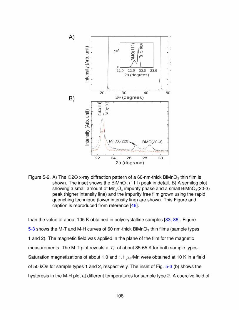
B)
A)
Figure 5-2. A) The Θ2Θ x-ray diffraction pattern of a 60-nm-thick BiMnO3 thin film isshown. The inset shows the BiMnO3 (111) peak in detail. B) A semilog plotshowing a small amount of Mn2O3 impurity phase and a small BiMnO3(20-3)peak (higher intensity line) and the impurity free film grown using the rapidquenching technique (lower intensity line) are shown. This Figure andcaption is reproduced from reference [46].
than the value of about 105 K obtained in polycrystalline samples [83, 86]. Figure
5-3 shows the M-T and M-H curves of 60 nm-thick BiMnO3 thin films (sample types
1 and 2). The magnetic field was applied in the plane of the film for the magnetic
measurements. The M-T plot reveals a TC of about 85-65 K for both sample types.
Saturation magnetizations of about 1.0 and 1.1 µB /Mn were obtained at 10 K in a field
of 50 kOe for sample types 1 and 2, respectively. The inset of Fig. 5-3 (b) shows the
hysteresis in the M-H plot at different temperatures for sample type 2. A coercive field of
108

about 270 Oe is observed at 10 K, which drops to about 30 Oe at 50 K. The hysteresis
of the M-H curves and the magnetic moment become negligible at about 80 K, which
is close to the estimated TC , confirming that the observed magnetization is associated
with magnetic ordering that happens at a temperature lower than the corresponding
TC of bulk BiMnO3 [83]. The reduced magnetic moment of our thin films compared to
bulk BiMnO3 is not due to the presence of the nonmagnetic impurities because both the
sample types 1 and 2 have similar saturation magnetizations and coercive fields.
Finally, the inset of Fig. 5-3 shows the surface morphology of sample type 2.
Both type 1 and 2 thin films show three-dimensional (3-D) island growth mode with
an r.m.s roughness of about 10 nm. It has been shown that 3-D island growth leads
to nonuniform strain resulting in high values of strains at the island edges [87, 88].
Because the crystal structure of BiMnO3 is closely related to that of antiferromagnetic
LaMnO3, the nonuniform strain distribution could be responsible for both the reduced
values of TC and the saturation magnetization.
5.2.3 Resistive Characterization
One of the most important qualities of a potentially ferroelectric sample is a large
resistivity, as the free charge carriers in low resistance materials would screen the
ferroelectric polarization, rendering it undetectable. In fact, this has been the primary
limitation in many thin film BiMnO3 multiferroic studies. Our optimized thin films have
a room temperature resistivity of about 10 Ω-cm, which is lower than values reported
by other groups [25, 89] However, by 140 K (below 140 K the resistance is too high to
measure with our instrumentation), the resistivity increases to about 1 MΩ-cm, and it
was possible to make direct polarization versus electric field (P-E) measurements at
temperatures below ≈ 100 K.
5.2.4 Ferroelectric Characterization
Ferroelectric measurements typically utilize a capacitor structure, the simplest
of which is a tri-layer metal-insulator-metal structure. However, due to the insulating
109

A)
B)
Figure 5-3. A) The magnetization vs temperature (M-T) plot for two 60-nm-thick BiMnO3thin films in an in-plane field of 500 Oe are shown: sample 1 (circles) andsample 2 (triangles). The full symbols and open symbols are the zero fieldcooled and field cooled data respectively. The inset shows a 5x5 µm atomicforce microscope image of the surface of sample 2. B) The magnetization vsmagnetic field (M-H) plot for sample 1 (circle) and sample 2 (triangle) at 10 Kare shown. The inset shows the reduction in the hysteresis of the M-H datafor sample 2 as the temperature is increased. This Figure and caption isreproduced from reference [46].
110

-100 -50 0 50 100-30
-20
-10
0
10
20
30
Rem
anen
t Pol
ariz
atio
n (
C/c
m2 )
E (kV/cm)
100K
100K
5K 0.00
0.25
0.50
0.75
1.000 50 100
M RP
Temperature
RP
& M
Figure 5-4. Remanent polarization hysteresis loops are shown. The ferroelectrictransition is shown to span ≈ 100 K, opening near 100 K with a maximumremanent polarization of ≈ 23 µ C/cm2 at 5 K.
substrate (STO), we have implemented an interdigital capacitance geometry. The
capacitor is composed of alternating V+/V− electrodes uniformly spaced on the film
surface, which leads to equipotential planes intersecting the film between each pair of
electrodes, resulting in a capacitance between the projected areas of each electrode
within the film (see Sec. 2.4.3). The projected areas were calculated analytically using
conformal mapping and equating the capacitor thickness to half the electrode spatial
wavelength [47]. The polarization is then calculated by dividing the transferred charge
by this projected area. The polarization in a typical hysteresis loop is calculated by
integrating the total transferred charge during application of a bipolar triangular voltage
waveform, with contributions from leakage current, capacitance, and ferroelectric
domain switching. However, as described in detail in Sec. 2.5.2, we measure remanent
hysteresis loops, where the contributions from leakage and capacitance have been
eliminated through specific pulsing sequences.
111
The ferroelectric transition was found to span more than 100 K, with the remanent
polarization (RP) vs. electric field loops opening slowly near 100 K and the RP
increasing to 23 µC/cm2 at 5 K. Incorporating the remanent polarization into typical
hysteresis loops (which include the total polarization, see Sec. 2.5.3), this broad
transition would result in the slow “square-to-slim-loop” transition in temperature that is
typical in relaxor ferroelectrics[90]. Interestingly, the ferroelectric transition is found to
coincide with the ferromagnetic transition. The inset of Fig. 5-4a shows that both the
ferroelectric polarization and magnetization increase from zero simultaneously, signaling
their respective transitions and suggesting a strong coupling between the orderings (see
Chap. 6 for a complete discussion).
The ferroelectric polarization is also found to be highly tunable, and is modulated
by both magnetic fields (magnetoelectric coupling) and external strain (see sections 6.2
and 6.3, respectively). The strain coupling is much stronger than the ME coupling,
lowering the coercive field and increasing the RP by as much as 50% at modest
strains of less than 10−2%. The strain coupling is strongest at low temperatures, and
disappears above T ≈ 50 K. The strain coupling is also found to be extremely sensitive
to the orientation of the strain (discussed in Chap.
5.2.5 Dielectric Characterization
To gain further insight into the ferroelectric transition, we have also completed a
dielectric characterization. The complex capacitance was measured as a function of
temperature at 200 frequencies over the bandwidth 20 Hz - 1 MHz, from 5 K< T <300
K. The characterization reveals two dielectric relaxations both of which display strong
temperature and frequency dependence.
Analyzing the frequency dependence of the complex capacitance shows two distinct
loss peaks centered at 1/τ1 and 1/τ2, indicating dielectric relaxations (see Fig. 5-5). The
112
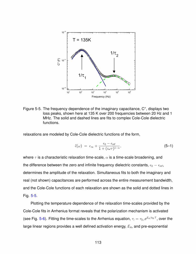
101 102 103 104 105 106
10-12
10-11
10-10
1/ 2
C'' (
F)
Frequency (Hz)
1/ 1
T = 135K
Figure 5-5. The frequency dependence of the imaginary capacitance, C′′, displays twoloss peaks, shown here at 135 K over 200 frequencies between 20 Hz and 1MHz. The solid and dashed lines are fits to complex Cole-Cole dielectricfunctions.
relaxations are modeled by Cole-Cole dielectric functions of the form,
ε(ω) = ε∞ +ε0 − εinf
1 + (iωτ)1−α, (5–1)
where τ is a characteristic relaxation time-scale, α is a time-scale broadening, and
the difference between the zero and infinite frequency dielectric constants, ε0 − εinf ,
determines the amplitude of the relaxation. Simultaneous fits to both the imaginary and
real (not shown) capacitances are performed across the entire measurement bandwidth,
and the Cole-Cole functions of each relaxation are shown as the solid and dotted lines in
Fig. 5-5.
Plotting the temperature dependence of the relaxation time-scales provided by the
Cole-Cole fits in Arrhenius format reveals that the polarization mechanism is activated
(see Fig. 5-6). Fitting the time-scales to the Arrhenius equation, τi = τ0,ieEA/kBT , over the
large linear regions provides a well defined activation energy, EA, and pre-exponential
113

6 9 1210-6
10-5
10-4
10-3
10-2 1
2
1 &
2
1000/T (K-1)
EA1 = 205meVEA2 = 189meV
Figure 5-6. Arrhenius plots of τ1 and τ1 are shown. Both relaxation time-scales arethermally activated, with activation energies of 205 meV and 189 meV,respectively.
factor for each loss peak. The activation energies are 205 ± 5 meV and 189 ± 4 meV,
with pre-factors of ≈ 2.9× 10⁻¹¹± 0.1× 10⁻¹¹ s and ≈ 3.610−13± 0.1× 10⁻¹³ s for τ1 and
τ2, respectively. We note that the pre-factors are quite small for a dielectric relaxation,
and are in the range of phonon frequencies.
Figure 5-7 shows the temperature dependence of the real component of the
complex capacitance for a selection of frequencies: 20 Hz, 200 Hz, and 2 kHz. At
high temperatures, there is evidence of a broad maximum, however, because of
the increased leakage the temperature range is limited and the peak is not directly
observed. The “maximum” is frequency dependent, however, occurring at higher
temperatures for higher frequencies. At low temperature, the dispersion disappears
and the real capacitance diverges (for reasons which are discussed below). The lack of
dispersion signifies that the capacitance is representative of the static dielectric constant
at our measurement frequencies.
114

0 50 100 150
0.1
0.2
0.3
0.4
0.5
C' (
nF)
Temperature (K)
20 Hz 200 Hz 2000 Hz
Figure 5-7. The temperature dependence of the real capacitance is shown for selectfrequencies. The high temperature range is limited due to increased leakagethere.
5.3 Nature of Ferroelectricity
5.3.1 Relaxor Review
Relaxor ferroelectricity can be understood by considering a representative model
called superparaelectricity [90], which is directly analogous to superparamagnetism,
except that in superparaelectricity the magnetic domains are replaced by ferroelectric
domains. Superparamagnets are typically composed of nano-sized magnetic
particles each of which act as their own ferromagnetic domain. In an applied field the
magnetic moments align resulting in a magnetization which is much larger than typical
paramagnets. However, once the field is removed the individual domains randomize
canceling the macroscopic magnetization over an activated time-scale known as the
Neel relaxation time. Below a certain temperature, the Neel relaxation time exceeds the
measurement time-scale and the system is said to be “blocked”, and behaves similar
to a regular ferromagnet. Relaxor ferroelectrics behave almost identically, with dipoles
originating from “polar-nano-regions” or PNRs. PNRs exhibit large induced polarizations
115

which reorient and randomize upon the removal of the electric fields. PNRs appear at
a high temperature transition, known as the Burns temperature (TB)[91], and grow in
size slowly with decreasing temperature until the freezing temperature. Then, at TF ,
the PNRs grow rapidly causing the fluctuation time-scales to diverge as a result of
the coalescing and coupling of neighboring PNRs[92, 93]. Besides their spontaneous
ferroelectric dipole moments, these regions have larger intrinsic dielectric constants as
well, leading to an increase in the overall dielectric constant as their % area increase at
TF .
In normal ferroelectrics, the ferroelectric transition is typically caused by a soft
long-wavelength phonon-mode that decreases to zero frequency at TC , resulting
in a static lattice deformation that extends throughout the crystal[94]. However,
relaxor ferroelectrics are inherently disordered by the PNRs which critically damp
the zone-center phonon modes and prohibit their propagation[95, 96]. As a result the
transition is very broad (diffuse), and the corresponding slow “slim to square loop”
transition in the hysteresis as the temperature is lowered is a signature of relaxor
behavior. The PNRs act as local “frozen phonon modes” that vibrate out of phase.
These vibrations are thermally activated and correspond to the flipping of PNR dipole
moments. PNRs contribute to the dielectric response via two distinct mechanisms: the
thermally activated reorientation of their dipole moments, and the displacement of their
boundaries[97]. The PNRs are also believed to cause the broad peak in ε′ as a function
of temperature, which is a classic signature of relaxor ferroelectricity[93].
5.3.2 Comparison
The first comparison to note between our data and the expected trends of relaxor
ferroelectricity is the diffuse (slow in temperature) ferroelectric transition. Figure 5-4
shows that the ferroelectric transition spans more than 100 K. If these remanent
polarization loops were incorporated into total polarization hysteresis loops (where
charge contributions from leakage and capacitance were included), it would result in a
116

slow “slim to square loop” hysteresis loop transition in temperature, which as discussed
is one of the primary signatures of relaxor ferroelectricity.
The dielectric data presented here also display all of the hallmarks of relaxor
ferroelectricity. First we note the presence of two relaxations is consistent with the two
dielectric mechanisms discussed above (PNR reorientation and boundary fluctuations).
The specific frequency dependence of the dielectric relaxations is also consistent with
PNRs. Phonon modes in typical dielectrics (ferroelectrics included) contribute to the
dielectric function according to the Lorentzian oscillator model:
ε = ε∞ +∑
j
Ajω2j
ω2j − ω2 − iγjω , (5–2)
where where ωj , γj , and Aj are the frequency, width, and dimensionless oscillator
strength of the jth phonon mode [98]. Phonon modes that are critically damped,
however, are instead represented by Cole-Cole dielectric functions instead (see Eq.
5–1) [64]. As shown in Fig. 5-5, the relaxations are both successfully modeled by
Cole-Cole functions.
The temperature dependence of the dielectric relaxations is also in agreement
with relaxor ferroelectricity. The relaxation time-scales are activated as expected
for PNR reorientation time-scales in the superparaelectric model, and fitting the
temperature dependence of the relaxation time-scales (provided by the Cole-Cole
fits) to the Arrhenius equation, τi = τ0,ieEA/kBT , results in quite small pre-exponential
factors of τ0,1 ≈ 3 × 10⁻¹¹ and τ0,2 ≈ 3.5 × 10⁻¹³, clearly establishing their phonon
origin of the PNRs (see Fig. 5-8. The real capacitance, shown in Fig. 5-7, is also
consistent with PNRs and relaxor ferroelectricity. At high temperatures we see evidence
of the tail end of the characteristic frequency dependent maximum (we are limited to
lower temperatures due to leakage) - a hallmark of relaxor ferroelectricity - and at low
temperatures we see a frequency independent divergence of the dielectric constant as
is expected with the rapid growth of the PNRs at the freezing temperature.
117

0 4 8 1210-14
10-12
10-10
10-8
10-6
10-4
10-2
100
Phonon Frequencies
1
2
1 &
21000/T (K-1)
Loop Time-scale
TC
Figure 5-8. The relaxation time-scales are extrapolated using the Arrhenius equation. Atlow temperatures the time-scale of the PNR dipole reorientations is shown tointersect with the RP loop time-scale almost exactly at TC = 100K . At hightemperatures the pre-exponential factors are shown to be in the range ofphonon frequencies.
The most convincing evidence for relaxor ferroelectricity, however, is the accurate
prediction of the ferroelectric TC from the dielectric data. At high temperatures the
PNRs randomize quickly so that once the ferroelectric measurements are finished the
remanent polarization has completely randomized. As temperature is lowered, however,
the randomization is less and less complete. Therefore, one would expect that just
as the ferroelectric hysteresis loops are opening that the measurement time-scale is
just equal to the PNR reorientation time-scale. As shown in Fig. 5-8, extrapolating the
activated time-scales via the Arrhenius equation, we see that the temperature at which
the PNR reorientation time-scale, τ1, and the RP loop measurement time-scale are
equal corresponds exactly to the temperature where the RP loops begin to open (TC ),
confirming the PNRs as the source of ferroelectricity.
5.3.3 Pulse Sequencing
As a final check of relaxor ferroelectricity, we study a simple two pulse waveform
depicted schematically in the inset of Fig. 5-9. The first voltage pulse poles the domains,
and the second voltage is applied after a variable delay time. After the second pulse is
118

applied a charge transfer measurement is conducted (green point in the inset of Fig.
5-9) to determine if any ferroelectric domains have reoriented during the delay time. The
charge transfer due to resistive leakage and capacitive charging should be the same
for each pulse independent of delay time, therefore any change in charge transfer with
delay time is attributed to reoriented ferroelectric domains. It is worth noting that this
procedure is distinct from the remanent polarization measurement procedure discussed
in Sec. 2.5.3. In the remanent polarization measurement, there are presetting pulses
which pole the domains, however, the charge transfer is only measured during the
following triangular waveform. Here the charge transfer is measured only as a result of
the pulse itself.
In a normal ferroelectric, the second pulse of our two pulse waveform should have
no effect as there should be minimal domain reorientations. In a relaxor ferroelectric,
however, the charge transfered during the second pulse should increase as the delay
time between pulses increases allowing time for more reorientations. The inset of Fig.
5-9 shows that the charge transfered by the second pulse increases logarithmically
with delay time, once again confirming the presence of rapidly disordering ferroelectric
domains, i.e. relaxor ferroelectricity.
5.3.4 Island Growth
Recent electron and neutron diffraction data have cast doubt over the purported
non-centrosymmetry of the BiMnO3 crystal structure [99], and centrosymmetric
structures have also been predicted using density functional theory calculations
[100]. This point is of fundamental importantance because a non-centrosymmetric
crystal structure is essential for ferroelectricity. Therefore, although BiMnO3 was first
thought a prime example of multiferroicity, there has been a growing debate concerning
whether it is an intrinsic ferroelectric. If the crystal structure of BiMnO3 is indeed
centrosymmetric, then the possible reasons for the ferroelectric behavior of BiMnO3 thin
films are: 1 structural distortions due to oxygen vacancies [99, 101], a centrosymmetric
119

0.0 0.5 1.0 1.5 2.0 2.5 3.04
6
8
10
Delay (s)
P (
C/c
m2 )
T = 90K
DelayV
time
0T
Measurement
Figure 5-9. The switched polarization is shown to increase with delay time betweenpulses, confirming the quick reorientation of PNRs. Inset: Schematic of thesimple pulse sequence.
to noncentrosymmetric transition below TC that is, below 100 K [24, 99], and substrate
induced strain [102].
Although, the Auger electron spectroscopy measurements on our thin films reveal
an oxygen deficiency that could lead to the ferroelectric behavior, we cannot rule out
the role of substrate induced strain. If the film is uniformly strained, the lattice mismatch,
which is -0.77% (compressive), is not enough to break the centrosymmetry as shown by
Hatt et al [102]. However, it has been shown that compressive lattice mismatch strain
could lead to a nonunifrom strain distribution in the thin film due to island formation
and the strain at the island edges could far exceed the average lattice mismatch strain
[87, 88]. The growth morphology of our thin films ( see the inset of Fig. 5-3) suggests
that such nonuniform strain distribution is also a possible mechanism for the appearance
of ferroelectricity. It is also worth noting that this interpretation is consistent with relaxor
ferroelectricity. The individual island edges would serve as PNRs, and the inherent
120

disorder of island growth explains the dampening of the phonon modes discussed
above.
5.4 Summary
In summary, impurity free multiferroic thin films of BiMnO3 (111) on SrTiO3 (001)
substrates have been grown with the desired structure and stoichiometry. The results
of structural, magnetic, resistive, ferroelectric, and dielectric characterizations were
also presented. The films are shown to be ferromagnetic with a TC of is 85-65 K and
a saturation magnetization of about 1 µB /Mn at 10 K. Also, the films demonstrated a
sufficiently high resistivity at low temperatures to allow the clear measurement of P-E
loops, and a ferroelectric remnant polarization of 23 µC/cm2 was measured at 5 K.
Finally, correlations between the dielectric and ferroelectric properties show that BiMnO3
is a relaxor ferroelectric, and it suspected that the PNR dipoles are located near island
edges.
As a caveat, it is appropriate to also mention an additional potential source of the
ferroelectric polarization presented in this chapter. Bismuth doped SrTiO3 is a well
known relaxor ferroelectric, and it is possible that during the pulsed laser deposition
some Bi ions may be implanted in the top layers of the substrate. However, we have
also grown BiMnO3 on LSAT and NGO substrates, which show small but non-zero
ferroelectric polarizations. Furthermore, the reduced polarization values are expected as
compressive strain decreases the ferroelectric polarization (see Sec. 6.2.1) and LSAT
and NGO substrates induce much larger compressive strains than STO. Therefore the
thin film BiMnO3 researched in this thesis is believed to display ferroelectric polarization
(potentially limited to island edges only).
121

CHAPTER 6TUNING FERROELECTRICITY IN BIMNO3
6.1 Introduction
Ferromagnetic and ferroelectric materials are ubiquitous in modern technology.
The vast majority of data storage technologies use magnetic materials, and the sensor
and actuator industries rely heavily on ferroelectric components. Multiferroics are
exciting because they offer the potential of one multi-functional material performing more
than one task. Furthermore, multiferroics are prime candidates for the technological
implementation of magnetoelectric coupling, offering an additional dimension to the
design phase-space and undoubtedly facilitating efficiency and progress. In particular,
magnetoelectric coupling could one day lead to the writing and reading of magnetic data
with electric fields, a capability that would decrease the power usage and increase the
speed of nearly every device involving memory. Additional devices proposed include
high-resolution magnetic field sensors, electrically tunable microwave applications such
as filters, oscillators and phase-shifters, and spintronic applications such as spin-wave
generation, amplification, and frequency conversion. However, the technological
implementation of multiferroic materials hinges on their ability to couple to external
perturbations.
In this chapter we will demonstrate that BiMnO3 shows multi-functional
characteristics, displaying strong couplings to both external strains and magnetic
fields. External strains of less than 10−2% change in lattice constants are shown
to increase the ferroelectric polarization by almost 50%. The strain coupling is also
shown to be anisotropic, sensitive only for specific induced distortions. Magnetic
fields of 7 T are found to decrease the ferroelectric polarization by 10%. While the
magnetoelectric coupling is small compared to the strain coupling, it is important to note
that while commonly discussed theoretically, direct observation of tuning of ferroelectric
polarization by magnetic fields is rare. Interestingly, all these properties appear to
122

be connected as the couplings are shown to correlate with each other through a low
temperature transition in the lattice.
6.2 Strain: External and Island Edges
6.2.1 External Strain
Stress is applied to the thin films directly using an external three-point beam
bending technique. In this technique the film is supported on opposite edges while
an external force is applied in the center of the film. The result is a bending of the film
similar to a classical beam, where the strain is quantified as,
ε = ∆L/L0 = xt/L20, (6–1)
where ∆L is the change in length at the surface of the beam due to a small displacement
(x) of the beam center, and L0 and t are the original length and thickness of the beam,
respectively. This strain can be either compressive or tensile depending on whether the
force is applied to the film surface or to the back-side of the substrate, as shown in Fig.
6-1, and is nominally uniaxial. The stress is applied by turning a 60 turns/inch screw in
contact with the sample surface with the aid of a worm gear providing spatial resolution
of ≈ 1 µm displacements.
The remanent polarization was found to depend strongly on externally applied
stress, and increases of almost 50% were observed at very modest strains of less than
10−2% change in lattice constants (see Fig. 6-2). The effect was found to be odd in
strain, with the sign of the change in polarization depending on whether compressive
or tensile strain was applied. The top inset of Fig. 6-2 shows that the coupling is linear
in strain at low strains, with the coupling diminishing at high strains. The bottom inset
of Fig. 6-2 show that the strain coupling displays strong temperature dependence,
appearing below approximately 50 K and diverging at low temperautres.
123

Figure 6-1. The three-point beam bending technique for applying compressive andtensile strain to a thin film is shown. When the film is on the opposite side ofthe applied stress (orange) the strain is tensile. When the film is on the sameside as the applied stress (purple), the strain is compressive. The areabetween the orange and purple lines represents the substrate. The dashedbox is the undistorted beam/substrate. Figure reproduced from [45].
-80 0 80-40
-30
-20
-10
0
10
20
30
40
Rem
anen
t Pol
ariz
atio
n (
C/c
m2 )
T = 5K
E (kV/cm)
5KS = 10-2%
0
5
100 25 50 75
Temperature
RP
2 4 6 8
0
5
10
10-3%)
R
P
Figure 6-2. An external strain of less than 10−2 is shown to increase the FE polarizationby ≈ 50% (blue curve). Insets: (upper) The strain coupling is shown toincrease as a function of tensile strain. (lower) The strain coupling is shownto decrease as a function of temperature, disappearing near ≈ 50 K.
124
6.2.2 Electrode “Lensing”
Advantageously, the interdigital capacitance geometry facilitates a “lensing”
experiment where the polarization may be probed as a function of the relative
orientations of the induced strain and applied electric field (see Fig. 6-3). Applying strain
along the (100) and (010) axes produced no change in remanent polarization regardless
of electric field orientation. Straining along (110) and (1-10), however, produces the
giant changes shown in Fig. 6-2. The increase is only for electric fields parallel to the
strain, with perpendicular fields inducing no change in remanent polarization (see Fig.
6-3). The insensitivity of the perpendicular fields rules out a rotation of the polarization,
suggesting that the strain induces ferroelectric polarization by stabilizing the monoclinic
ferroelectric distortion of BiMnO3 (see Fig. 6-3).
6.2.3 Island Edge Strain Gradients
With a SrTiO3 substrate, the lattice mismatch strain for BiMnO3 is approximately
-0.77% (compressive), which according to density functional theory calculations is not
sufficient to break centrosymmetry and induce ferroelectricity [102]. Furthermore, the
externally applied strain is not sufficiently large either. Therefore another factor that is
sensitive to strain must be present: island edge strain gradients.
Compressive lattice mismatch strain can lead to a non-unifrom strain distribution in
thin film due to island formation, and the strain at the island edges can far exceed the
average lattice mismatch strain (see Fig. 6-4) [87, 88]. The growth morphology of our
thin films (see Fig. 5-3) suggests that such non-uniform strain distribution is a definite
possible mechanism for the appearance of ferroelectricity. Additionally, this mechanism
explains the high sensitivity to external strain. As shown in the inset of Fig. 5-3, the
strain gradients diverge near the island edge. Therefore, it is likely that our externally
applied strain converts the regions near the island edges just short of the critical strain
necessary to produce ferroelectric polarization.
125

A)
B)
Figure 6-3. A) The schematic shows the orientations of the electric fields and inducedstrains. The remanent polarization is insensitive to < 100 > and < 010 >strains, however, < 110 > and < 1− 10 > strains induce/stabilize themonoclinic ferroelectric distortion of BiMnO3. Only electrodes with electricfields parallel to the induced tensile strains detect changes (increases),meaning the RP does not rotate, but that new ferroelectric dipoles arecreated as the PNRs grow. B) Arrows indicate the monoclinic distortions ofthe unit cell induced by straining along < 110 > and < 1− 10 >. Bi is blue, Ois red, and Mn is yellow.
6.3 Magnetoelectric Coupling in BiMnO3
6.3.1 Remanent Polarization Tuning
In addition to strain tuning, the ferroelectric polarization is also modulated by
external magnetic fields. This magnetoelectric coupling is shown in Fig. 6-5, where the
remanent polarization is shown to decrease by approximately 10% in a field of 7 T. The
coercive field is unchanged, with only the magnitude of the polarization effected, and the
coupling is isotropic - equivalent for all angles of applied fields.
The magnetoelectric coupling is shown to be linear in field (upper inset of Fig. 6-5),
with a maximum linear magnetoelectric coupling coefficient of, α = 0.1 µC/cm2T near
126

C)
B)
D)
A)
Figure 6-4. A) An AFM image shows Ge islands grown on a Si substrate. B) Across-section TEM image shows a Ge island on a 6 monolayer thick Gewetting layer on a Si substrate. C) The boundary of Lings mound and acontour diagram shows the calculated strain εxx in the system. D) Thevariation of surface strain εs is shown along the system surface. The figure isreproduced from reference [88].
65 K (see Sec. 1.3.3. The magnetoelectric coupling is also found to decrease with
temperature, disappearing completely below T ≈ 50K (see lower inset of Fig. 6-5).
6.3.2 Reorientation Time-Scales
To investigate the magnetoelectric coupling further, we also checked the magnetic
field dependence of our dual pulse waveform introduced in Sec. 5.3.3 (where an intitial
pulse poles the ferroelectric domains, and after a variable delay time a second pulse
checks for domains which have reoriented). Figure 6-6 shows the result of varying
the delay time between pulses for both 0 T and 7 T fields. As seen, for all delay times,
the magnetic field data have larger measured switching polarizations. Therefore, we
conclude that the magnetic field decreases the reorientation time-scale so that more
PNRs are available to flip during the second pulse. The dielectric data also support this
127
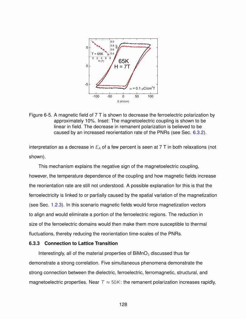
-100 -50 0 50 100
-5
0
5
= 0.1 C/cm2T
H = 7T
E (kV/cm)
65KT = 65K0 2 4 6 8
5.45.65.86.0
RP
H (T)
Figure 6-5. A magnetic field of 7 T is shown to decrease the ferroelectric polarization byapproximately 10%. Inset: The magnetoelectric coupling is shown to belinear in field. The decrease in remanent polarization is believed to becaused by an increased reorientation rate of the PNRs (see Sec. 6.3.2).
interpretation as a decrease in EA of a few percent is seen at 7 T in both relaxations (not
shown).
This mechanism explains the negative sign of the magnetoelectric coupling,
however, the temperature dependence of the coupling and how magnetic fields increase
the reorientation rate are still not understood. A possible explanation for this is that the
ferroelectricity is linked to or partially caused by the spatial variation of the magnetization
(see Sec. 1.2.3). In this scenario magnetic fields would force magnetization vectors
to align and would eliminate a portion of the ferroelectric regions. The reduction in
size of the ferroelectric domains would then make them more susceptible to thermal
fluctuations, thereby reducing the reorientation time-scales of the PNRs.
6.3.3 Connection to Lattice Transition
Interestingly, all of the material properties of BiMnO3 discussed thus far
demonstrate a strong correlation. Five simultaneous phenomena demonstrate the
strong connection between the dielectric, ferroelectric, ferromagnetic, structural, and
magnetoelectric properties. Near T ≈ 50K : the remanent polarization increases rapidly,
128
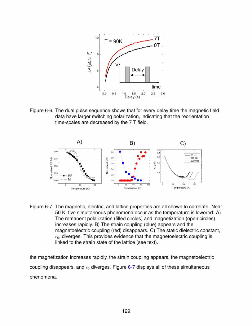
0.0 0.5 1.0 1.5 2.0 2.5 3.0
4
6
8
10
Delay (s)
P (
C/c
m2 )
T = 90K
DelayV
time
7T0T
Figure 6-6. The dual pulse sequence shows that for every delay time the magnetic fielddata have larger switching polarization, indicating that the reorientationtime-scales are decreased by the 7 T field.
C)B)
0 50 100
0.00
0.25
0.50
0.75
1.00
RP M
Temperature (K)
Nor
mal
ized
RP
& M
0 50 100 150
0.1
0.2
0.3
0.4
0.5
C' (
nF)
Temperature (K)
20 Hz 200 Hz 2000 Hz
0 25 50 75 100
0.0
0.2
0.4
0.6
0.8
1.0
Temperature (K)
Nor
mal
ized
R
P
A)
Figure 6-7. The magnetic, electric, and lattice properties are all shown to correlate. Near50 K, five simultaneous phenomena occur as the temperature is lowered. A)The remanent polarization (filled circles) and magnetization (open circles)increases rapidly. B) The strain coupling (blue) appears and themagnetoelectric coupling (red) disappears. C) The static dielectric constant,ε0, diverges. This provides evidence that the magnetoelectric coupling islinked to the strain state of the lattice (see text).
the magnetization increases rapidly, the strain coupling appears, the magnetoelectric
coupling disappears, and ε0 diverges. Figure 6-7 displays all of these simultaneous
phenomena.
129

The rapid increase in the remanent polarization tells us the PNR vibrations have
slowed down significantly (and are growing), indicating a stiffening of the lattice (see Fig.
6-7 (a)). This is also suggested by the appearance of the strain coupling (see Fig. 6-7
(b)), indicating that the lattice is now rigid enough to hold the induced distortions. The
cause of the change in the lattice is not clear, however, the coincidence of the increase
in magnetization suggests ferrodistortion is likely (see Fig 6-7 (a)). The increase in
dielectric constant indicates PNRs are likely increasing in size (see Fig. 6-7 (c)). These
phenomena suggest that 50 K is the freezing temperature known in relaxor ferroelectrics
(where fluctuation time-scales diverge, and the PNRs coalesce and couple). The
simultaneous disappearance of magnetoelectric coupling suggests its mechanism is
tied to the flexibility of the lattice (see Fig. 6-7 (b)), consistent with a recent theoretical
prediction of giant magnetoelectric coupling induced by ’structural softness’ [103].
6.4 Summary
In this chapter we demonstrated that the ferroelectric polarization in BiMnO3 may
be modulated in two distinct manners: external strain coupling, and magnetoelectric
coupling. The external strain tuning showed an increase of more than 50% in the
ferroelectric polarization when the strain was oriented to induce monoclinic distortions.
The magnetoelectric coupling manifested a 10% decrease in ferroelectric polarization
in fields of 7 T. Furthermore, these couplings provided a window into the mechanism
driving the multiferroic behavior: The low levels of strain required to increase the
ferroelectricity (less than 10−2%) suggest the large strain gradient regions near island
edges allow regions with strain just below the critical strain for ferroelectricity to be
converted. Also, the magnetic field was shown to alter the reorientation time-scales of
the PNRs providing insight into the relaxor nature of the ferroelectricity.
130

REFERENCES
[1] G. H. Jonker and J. H. V. Santen, Physica 16, 337 (1950)
[2] S. Jin, T. H. Tiefel, M. McCormack, R. A. Fastnacht, R. Ramesh, and L. H. Chen,Science 264, 413 (1994)
[3] E. Dagotto, Nanoscale Phase Separation and Colossal Magnetoresistance, 1sted. (Springer, 2003) ISBN 3540432450
[4] H. Jahn and E. Teller, Proceedings of the Royal Society of London, Series A:Mathematical and Physical Sciences 161, 220 (July 1937)
[5] C. Zener, Phys. Rev. 82, 403 (May 1951)
[6] P. W. Anderson and H. Hasegawa, Phys. Rev. 100, 675 (Oct 1955)
[7] N. Mathur and P. Littlewood, Solid State Communications 119, 271 (2001)
[8] S. A. Wolf, D. D. Awschalom, R. A. Buhrman, J. M. Daughton, S. von Molnr,M. L. Roukes, A. Y. Chtchelkanova, and D. M. Treger, Science 294, 1488 (2001),http://www.sciencemag.org/content/294/5546/1488.abstract
[9] A. J. Millis, B. I. Shraiman, and R. Mueller, Phys. Rev. Lett. 77, 175 (Jul 1996)
[10] P. W. Anderson, Phys. Rev. 79, 350 (Jul 1950)
[11] J. B. Goodenough, Phys. Rev. 100, 564 (Oct 1955)
[12] A. J. Millis, Nature 392, 147 (Mar. 1998)
[13] R. P. Rairigh, Colossal magnetocapacitance and scale-invariant dielectric re-sponse in phase-separated manganites, Ph.D. thesis, University of Florida (2006)
[14] Y. Tomioka, A. Asamitsu, H. Kuwahara, Y. Moritomo, and Y. Tokura, Phys. Rev. B53, R1689 (Jan 1996)
[15] W. Prellier, C. Simon, A. M. Haghiri-Gosnet, B. Mercey, and B. Raveau, Phys. Rev.B 62, R16337 (Dec 2000)
[16] M. Uehara, S. Mori, C. H. Chen, and S.-W. Cheong, Nature 399, 560 (Jun. 1999)
[17] L. Zhang, C. Israel, A. Biswas, R. L. Greene, and A. de Lozanne, Science 298,805 (2002)
[18] R. P. Rairigh, G. Singh-Bhalla, S. Tongay, T. Dhakal, A. Biswas, and A. F. Hebard,Nat. Phys. 3, 551 (Aug. 2007)
[19] H. Schmid, Ferroelectrics 162, 317 (1994)
[20] G. A. Smolenski and I. E. Chupis, Soviet Physics Uspekhi 25, 475 (1982)
131

[21] Y. N. Venevtsev and V. V. Gagulin, Ferroelectrics 162, 23 (1994)
[22] S.-W. Cheong and M. Mostovoy, Nat. Mater. 6, 13 (Jan. 2007)
[23] R. Ramesh and N. A. Spaldin, Nature Materials 6, 21 (Jan. 2007)
[24] N. A. Spaldin and M. Fiebig, Science 309, 391 (2005)
[25] W. Eerenstein, N. D. Mathur, and J. F. Scott, Nature 442, 759 (Aug. 2006)
[26] D. Khomskii, J. Magn. Magn. Mater. 306, 1 (2006)
[27] N. A. Hill, Journal of Physical Chemistry B 104, 6694 (2000)
[28] T. Kimura, T. Goto, H. Shintani, K. Ishizaka, T. Arima, and Y. Tokura, Nature 426,55 (Nov. 2003)
[29] N. Ikeda, H. Ohsumi, K. Ohwada, K. Ishii, T. Inami, K. Kakurai, Y. Murakami,K. Yoshii, S. Mori, Y. Horibe, and H. Kito, Nature 436, 1136 (Aug. 2005)
[30] M. Fiebig, T. Lottermoser, D. Frohlich, A. V. Goltsev, and R. V. Pisarev, Nature 419,818 (Oct. 2002)
[31] P. Peier, S. Pilz, F. Muller, K. A. Nelson, and T. Feurer, J. Opt. Soc. Am. B 25, B70(Jul 2008)
[32] J. F. Scott, J. Phys.: Condens. Matter 20, 021001 (2008)
[33] K. F. Wang, J. M. Liu, and Z. F. Ren, Advances in Physics 58, 321 (2009)
[34] E. Bousquet, M. Dawber, N. Stucki, C. Lichtensteiger, P. Hermet, S. Gariglio, J.-M.Triscone, and P. Ghosez, Nature 452, 732 (Apr. 2008)
[35] D. V. Efremov, J. van den Brink, and D. I. Khomskii, Nat. Mater. 3, 853 (Dec. 2004)
[36] M. Mostovoy, Phys. Rev. Lett. 96, 067601 (Feb 2006)
[37] R. Levitin, E. Popova, R. Chtsherbov, A. Vasiliev, M. Popova, E. Chukalina,S. Klimin, P. van Loosdrecht, D. Fausti, and L. Bezmaternykh, JETP Lett. 79, 423(2004), 10.1134/1.1776236
[38] H. Zheng, J. Wang, S. E. Lofland, Z. Ma, L. Mohaddes-Ardabili, T. Zhao,L. Salamanca-Riba, S. R. Shinde, S. B. Ogale, F. Bai, D. Viehland, Y. Jia, D. G.Schlom, M. Wuttig, A. Roytburd, and R. Ramesh, Science 303, 661 (2004)
[39] F. Zavaliche, H. Zheng, L. Mohaddes-Ardabili, S. Y. Yang, Q. Zhan, P. Shafer,E. Reilly, R. Chopdekar, Y. Jia, P. Wright, D. G. Schlom, Y. Suzuki, andR. Ramesh, Nano Lett. 5, 1793 (2005)
[40] R. Seshadri and N. A. Hill, Chem. Mater. 13, 2892 (2001)
132
[41] M. Fiebig, J. Phys. D: Appl. Phys. 38, R123 (2005)
[42] W. Roentgen, Ann. Phys. 35, 264 (1888)
[43] H. A. Wilson, Philosophical Transactions of the Royal Society of London. Series A,Containing Papers of a Mathematical or Physical Character 204, 121 (1905)
[44] M. M. Parish and P. B. Littlewood, Phys. Rev. Lett. 101, 166602 (Oct 2008)
[45] J. Tosado, T. Dhakal, and A. Biswas, J. Phys.: Condens. Matter 21, 192203 (2009)
[46] H. Jeen, G. Singh-Bhalla, P. R. Mickel, K. Voigt, C. Morien, S. Tongay, A. F.Hebard, and A. Biswas, J. Appl. Phys. 109, 074104 (2011)
[47] R. Igreja and C. J. Dias, Sensors and Actuators, A: Physical 112, 291 (2004)
[48] K. M. Lang, V. Madhavan, J. E. Hoffman, E. W. Hudson, H. Eisaki, S. Uchida, andJ. C. Davis, Nature 415, 412 (Jan. 2002)
[49] V. J. Emery, S. A. Kivelson, and H. Q. Lin, Phys. Rev. Lett. 64, 475 (Jan 1990)
[50] J. Hemberger, P. Lunkenheimer, R. Fichtl, H.-A. Krug von Nidda, V. Tsurkan, andA. Loidl, Nature 434, 364 (Mar. 2005)
[51] M. P. Singh, W. Prellier, L. Mechin, and B. Raveau, Appl. Phys. Lett. 88, 012903(2006)
[52] Y. J. Choi, C. L. Zhang, N. Lee, and S.-W. Cheong, Phys. Rev. Lett. 105, 097201(Aug 2010)
[53] E. Dagotto, Science 309, 257 (2005)
[54] A. Banerjee, A. K. Pramanik, K. Kumar, and P. Chaddah, J. Phys.: Condens.Matter 18, 605 (2006)
[55] A. Nucara, P. Maselli, P. Calvani, R. Sopracase, M. Ortolani, G. Gruener, M. C.Guidi, U. Schade, and J. Garcıa, Phys. Rev. Lett. 101, 066407 (Aug 2008)
[56] H. J. Lee, K. H. Kim, M. W. Kim, T. W. Noh, B. G. Kim, T. Y. Koo, S.-W. Cheong,Y. J. Wang, and X. Wei, Phys. Rev. B 65, 115118 (Mar 2002)
[57] V. Kiryukhin, B. G. Kim, V. Podzorov, S.-W. Cheong, T. Y. Koo, J. P. Hill, I. Moon,and Y. H. Jeong, Phys. Rev. B 63, 024420 (Dec 2000)
[58] S. Cox, J. Singleton, R. D. McDonald, A. Migliori, and P. B. Littlewood, Nat. Mater.7, 25 (Jan. 2008)
[59] C. Barone, A. Galdi, N. Lampis, L. Maritato, F. M. Granozio, S. Pagano, P. Perna,M. Radovic, and U. Scotti di Uccio, Phys. Rev. B 80, 115 (Sep 2009)
133

[60] N. P. Ong, J. W. Brill, J. C. Eckert, J. W. Savage, S. K. Khanna, and R. B.Somoano, Phys. Rev. Lett. 42, 811 (Mar 1979)
[61] P. Chaikin, W. Fuller, R. Lacoe, J. Kwak, R. Greene, J. Eckert, and N. Ong, SolidState Communications 39, 553 (1981)
[62] J. Tao and J. M. Zuo, Phys. Rev. B 69, 180404 (May 2004)
[63] A. K. Jonscher, J. Phys. D: Appl. Phys. 32, R57 (1999)
[64] K. S. Cole and R. H. Cole, J. Chem. Phys. 9, 341 (1941)
[65] L. Wu, R. F. Klie, Y. Zhu, and C. Jooss, Phys. Rev. B 76, 174210 (Nov 2007)
[66] S. Bhattacharya, J. P. Stokes, M. J. Higgins, and R. A. Klemm, Phys. Rev. Lett. 59,1849 (Oct 1987)
[67] M. B. Salamon and M. Jaime, Rev. Mod. Phys. 73, 583 (Aug 2001)
[68] N. Biskup, A. de Andres, J. L. Martinez, and C. Perca, Phys. Rev. B 72, 024115(Jul 2005)
[69] R. S. Freitas, J. F. Mitchell, and P. Schiffer, Phys. Rev. B 72, 144429 (Oct 2005)
[70] J. L. Cohn, M. Peterca, and J. J. Neumeier, Phys. Rev. B 70, 214433 (Dec 2004)
[71] S. Havriliak and S. Negami, Polymer 8, 161 (1967)
[72] G. C. Milward, M. J. Calderon, and P. B. Littlewood, Nature 433, 607 (Feb. 2005)
[73] G. T. Rado, J. M. Ferrari, and W. G. Maisch, Phys. Rev. B 29, 4041 (Apr 1984)
[74] C. A. F. Vaz, J. Hoffman, C. H. Ahn, and R. Ramesh, Advanced Materials 22, 2900(2010)
[75] C.-W. Nan, M. I. Bichurin, S. Dong, D. Viehland, and G. Srinivasan, J. Appl. Phys.103, 031101 (2008)
[76] T. Goto, T. Kimura, G. Lawes, A. P. Ramirez, and Y. Tokura, Phys. Rev. Lett. 92,257201 (Jun 2004)
[77] Y. Moritomo, H. Kuwahara, Y. Tomioka, and Y. Tokura, Phys. Rev. B 55, 7549 (Mar1997)
[78] J. M. D. Teresa, M. R. Ibarra, P. A. Algarabel, C. Ritter, C. Marquina, J. Blasco,J. Garcia, A. del Moral, and Z. Arnold, Nature 386, 256 (Mar. 1997)
[79] G. Singh-Bhalla, S. Selcuk, T. Dhakal, A. Biswas, and A. F. Hebard, Phys. Rev.Lett. 102, 077205 (Feb 2009)
[80] N. A. Hill and K. M. Rabe, Phys. Rev. B 59, 8759 (Apr 1999)
134

[81] T. Atou, H. Chiba, K. Ohoyama, Y. Yamaguchi, and Y. Syono, J. Solid State Chem.145, 639 (1999)
[82] A. Moreira dos Santos, A. K. Cheetham, T. Atou, Y. Syono, Y. Yamaguchi,K. Ohoyama, H. Chiba, and C. N. R. Rao, Phys. Rev. B 66, 064425 (Aug 2002)
[83] A. M. dos Santos, S. Parashar, A. R. Raju, Y. S. Zhao, A. K. Cheetham, andC. N. R. Rao, Solid State Communications 122, 49 (2002)
[84] J. Y. Son and Y.-H. Shin, Applied Physics Letters 93, 062902 (2008)
[85] J. B. Goodenough, Phys. Rev. 100, 564 (Oct 1955)
[86] H. Chiba, T. Atou, and Y. Syono, Journal of Solid State Chemistry 132, 139 (1997)
[87] A. Biswas, M. Rajeswari, R. C. Srivastava, Y. H. Li, T. Venkatesan, R. L. Greene,and A. J. Millis, Phys. Rev. B 61, 9665 (Apr 2000)
[88] Y. Chen and J. Washburn, Phys. Rev. Lett. 77, 4046 (Nov 1996)
[89] M. Gajek, M. Bibes, A. Barthelemy, K. Bouzehouane, S. Fusil, M. Varela,J. Fontcuberta, and A. Fert, Phys. Rev. B 72, 020406 (Jul 2005)
[90] D. Viehland, J. F. Li, S. J. Jang, L. E. Cross, and M. Wuttig, Phys. Rev. B 43, 8316(Apr 1991)
[91] G. Burns and F. H. Dacol, Solid State Commun. 48, 853 (1983)
[92] R. Pirc and R. Blinc, Phys. Rev. B 76, 020101 (Jul 2007)
[93] S. B. Lang, H. L. W. Chan, A. A. Bokov, and Z. G. Ye, in Frontiers of Ferroelectric-ity (Springer US, 2007) pp. 31–52
[94] J. F. Scott, Rev. Mod. Phys. 46, 83 (Jan 1974)
[95] P. M. Gehring, S.-E. Park, and G. Shirane, Phys. Rev. Lett. 84, 5216 (May 2000)
[96] T. Tsurumi, K. Soejima, T. Kamiya, and M. Daimon, Jpn J Appl Phys 33, 1959(1994)
[97] V. Bovtun, J. Petzelt, V. Porokhonskyy, S. Kamba, and Y. Yakimenko, J. Eur.Ceram. Soc. 21, 1307 (2001)
[98] C. C. Homes, T. Vogt, S. M. Shapiro, S. Wakimoto, and A. P. Ramirez, Science293, 673 (2001), http://www.sciencemag.org/content/293/5530/673.abstract
[99] A. A. Belik, S. Iikubo, T. Yokosawa, K. Kodama, N. Igawa, S. Shamoto, M. Azuma,M. Takano, K. Kimoto, Y. Matsui, and E. Takayama-Muromachi, J. Am. Chem. Soc.129, 971 (2007)
[100] P. Baettig, R. Seshadri, and N. A. Spaldin, J. Am. Chem. Soc. 129, 9854 (2007)
135
[101] M. Gajek, M. Bibes, S. Fusil, K. Bouzehouane, J. Fontcuberta, A. Barthelemy, andA. Fert, Nat Mater 6, 296 (Apr. 2007), http://dx.doi.org/10.1038/nmat1860
[102] A. J. Hatt and N. A. Spaldin, European Physical Journal B: Condensed MatterPhysics 71, 435 (2009), 10.1140/epjb/e2009-00320-3
[103] J. C. Wojdeł and J. Iniguez, Phys. Rev. Lett. 105, 037208 (Jul 2010)
136

BIOGRAPHICAL SKETCH
Patrick R. Mickel was born in 1982 to two loving parents, Stan and Karen Mickel.
He was born into a family with two older brothers, Andy and Jeremy, where his parents
fostered all of their talents without pushing in preset directions (evidenced by their
diverse choices: art, writing, and science). As a child, his affinity for tools shined
through, as he was constantly building toys. He enjoyed some success - a full-scale
half-pipe for roller-blading and skateboarding, and a make-shift BB gun - as well as
some failures, such as a pressurized squirt-gun and battery powered moped (much to
his teasing friends’ delight). Although he excelled in math growing up, it was not until
late into high school that he discovered his love for physics.
During the second semester of his senior year, he enrolled in an astronomy course
at Wittenberg University, taught by the physics professor Dr. Daniel Fleisch - who
was famous on campus for his talent and charisma. Patrick would stay after class,
sometimes for hours, talking with Dr. Fleisch and learning about all different areas
of science. He was hooked. He started college at the University of Notre Dame the
following fall listed as a tentative theology/philosophy major, but quickly changed
course and majored in physics. During his undergraduate years, he sought a diverse
experience and volunteered for research in many different areas: high energy physics,
optics, statistical physics, and condensed matter.
His senior year he decided to apply for graduate school and pursue a Ph.D. in
physics (not surprising for the son of two academics). Then, under the guidance of a
few trusted physics professors, he accepted a fellowship from the University of Florida.
While initially focused on biophysics (Nuclear Magnetic Resonance diffusion tensor
imgaing), during his second year, he took a course with Dr. Arthur Hebard and quickly
realized how great an opportunity it would be to work with him. The next semester he
joined Art’s lab, and began the research that has culminated in this dissertation. Finally,
he graduate with his Ph.D. from the University of Florida in August of 2011.
137