soft-switching techniques for medium-voltage isolated ... · soft-switching techniques for...
TRANSCRIPT

© 2012 IEEE
Proceedings of the 38th Annual Conference of the IEEE Industrial Electronics Society (IECON 2012), Montreal, Canada,October 25-28, 2012
Soft-Switching Techniques for Medium-Voltage Isolated Bidirectional DC/DC Converters in SolidState Transformers
G. Ortiz,D. Bortis,J. W. Kolar,O. Apeldoorn
This material is published in order to provide access to research results of the Power Electronic Systems Laboratory / D-ITET / ETH Zurich. Internal or personal use of this material is permitted. However, permission to reprint/republish this material for advertising or promotional purposes or for creating new collective works for resale or redistribution must be obtained from the copyright holder. By choosing to view this document, you agree to all provisions of the copyright laws protecting it.
Soft-Switching Techniques for Medium-Voltage Isolated Bidirectional DCIDC Converters in Solid State Transformers
G. Ortiz*, D. Bortis*, 1. W. Kolar*, O. Apeldoorn**
*Power Electronic Systems Laboratory, ETH Zurich
**Power Electronics and Medium Voltage Drives, ABB Switzerland AG
Email: [email protected]
Abstract-Soft switching techniques are very attractive and often mandatory requirements in medium-voltage and medium-frequency
applications such as solid state transformers. The effectiveness of these soft switching techniques is tightly related to the dynamic behavior of the internal stored charge in the utilized semiconductor devices. For this reason, this paper analyzes the behavior of the internal charge dynamics in high-voltage semiconductors, giving a clear base to understand the previously proposed zero-current-switching techniques for IGBTbased resonant dual-active-bridges. From these previous approaches, the two main concepts that allow switching loss reduction in highvoltage semiconductors are identified: 1) shaping of the conducted current in order to achieve a high recombination time in the previously conducting semiconductors and 2) achieving ZVS in the turning-on device. The means to implement these techniques in a triangular current mode dual-active-bridge converter together with the benefits of the proposed approaches are analyzed and experimentally verified with a 1. 7 k V IGBT-based NPC bridge. Additionally, the impact of the modified currents in the converter's performance are quantified in order to determine the benefits of the introduced concepts in the overall converter.
I. INTRODUCTION
Transformers operating in line frequency (SO/60Hz) are key
components within today's electric power systems as they provide
the link between grids with different voltage levels, namely high
voltage, medium voltage (MV) and low voltage (LV) grids. These
transformers however, are characterized by several limitations such
as large size/weight, ideally equal input and output active and
reactive power, equal input and output operating frequency and
tightly linked input and output voltages.
These limitations can be overcome by building a transformer
based on power electronic devices, i.e. a Solid State Transformer
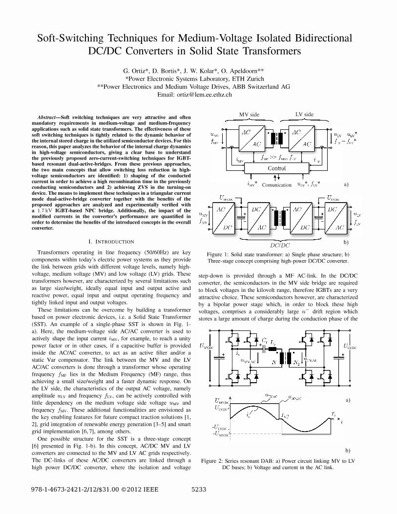
(SST). An example of a single-phase SST is shown in Fig. 1-
a). Here, the medium-voltage side AC/AC converter is used to
actively shape the input current iMV, for example, to reach a unity
power factor or in other cases, if a capacitive buffer is provided
inside the AC/AC converter, to act as an active filter and/or a
static Var compensator. The link between the MV and the LV
AC/AC converters is done through a transformer whose operating
frequency fMF lies in the Medium Frequency (MF) range, thus
achieving a small size/weight and a faster dynamic response. On
the LV side, the characteristics of the output AC voltage, namely
amplitude ULV and frequency Av, can be actively controlled with
little dependency on the medium voltage side voltage UMV and
frequency fMv. These additional functionalities are envisioned as
the key enabling features for future compact traction solutions [1,
2], grid integration of renewable energy generation [3-S] and smart
grid implementation [6,7], among others.
One possible structure for the SST is a three-stage concept
[6] presented in Fig. I-b). In this concept, AC/DC MV and LV
converters are connected to the MV and LV AC grids respectively.
The DC-links of these AC/DC converters are linked through a
high power DC/DC converter, where the isolation and voltage
978-1-4673-2421-2/12/$31.00 ©2012 IEEE
MV side LV side r _____ .Jo.-.... ___ '" r,----.Jo.-.... _-_'"
iMV * Comunication ULV *, flY *
�"" __________ � _________ J DC/DC
a)
b)
Figure 1: Solid state transformer: a) Single phase structure; b) Three-stage concept comprising high-power DC/DC converter.
step-down is provided through a MF AC-link. In the DC/DC
converter, the semiconductors in the MV side bridge are required
to block voltages in the kilovolt range, therefore IGBTs are a very
attractive choice. These semiconductors however, are characterized
by a bipolar power stage which, in order to block these high
voltages, comprises a considerably large n - drift region which
stores a large amount of charge during the conduction phase of the
I ULV,DC
+
UMV,DC;�========�====1
U�V,DC
a)
Ts
-U�V,DC
-UMV,DC
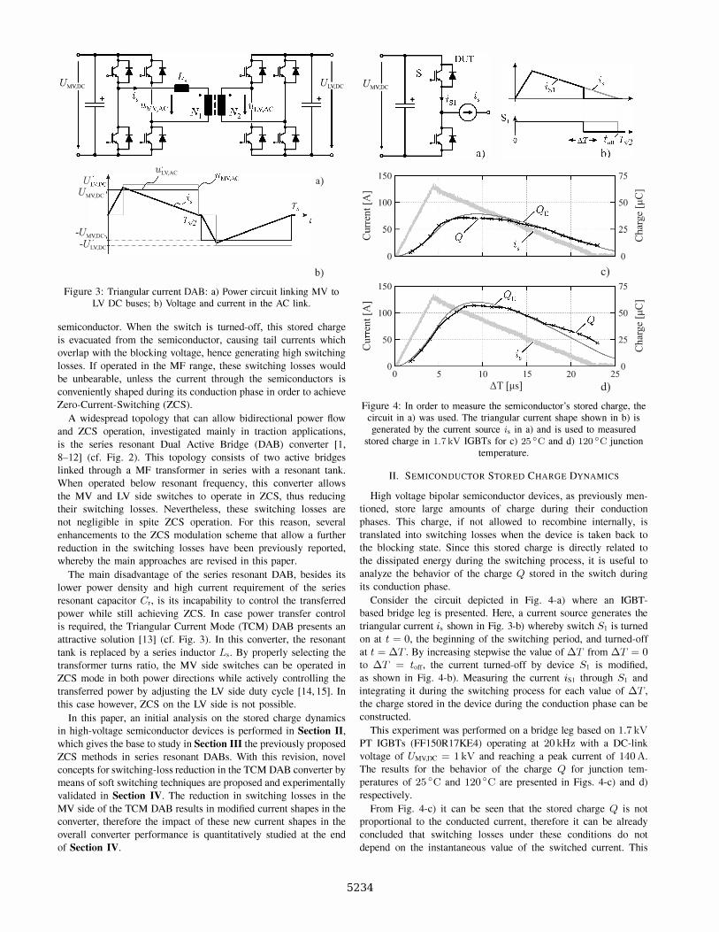
b) Figure 2: Series resonant DAB: a) Power circuit linking MV to LV
DC buses; b) Voltage and current in the AC link.
5233
I UMV,DC
I ULV,DC
+
ULY,AC
U �V'DC;f--JF.�Z::===::( UMV,DC
a)
-UMV,DC
-U�V,DC
b) Figure 3: Triangular current DAB: a) Power circuit linking MV to
LV DC buses; b) Voltage and current in the AC link.
semiconductor. When the switch is turned-off, this stored charge
is evacuated from the semiconductor, causing tail currents which
overlap with the blocking voltage, hence generating high switching
losses. If operated in the MF range, these switching losses would
be unbearable, unless the current through the semiconductors is
conveniently shaped during its conduction phase in order to achieve
Zero-Current-Switching (ZCS).
A widespread topology that can allow bidirectional power flow
and ZCS operation, investigated mainly in traction applications,
is the series resonant Dual Active Bridge (DAB) converter [1,
8-12] (cf. Fig. 2). This topology consists of two active bridges
linked through a MF transformer in series with a resonant tank.
When operated below resonant frequency, this converter allows
the MV and LV side switches to operate in ZCS, thus reducing
their switching losses. Nevertheless, these switching losses are
not negligible in spite ZCS operation. For this reason, several
enhancements to the ZCS modulation scheme that allow a further
reduction in the switching losses have been previously reported,
whereby the main approaches are revised in this paper.
The main disadvantage of the series resonant DAB, besides its
lower power density and high current requirement of the series
resonant capacitor Cr, is its incapability to control the transferred
power while still achieving ZCS. In case power transfer control
is required, the Triangular Current Mode (TCM) DAB presents an
attractive solution [13] (cf. Fig. 3). In this converter, the resonant
tank is replaced by a series inductor Ls. By properly selecting the
transformer turns ratio, the MV side switches can be operated in
ZCS mode in both power directions while actively controlling the
transferred power by adjusting the LV side duty cycle [14,15]. In
this case however, ZCS on the LV side is not possible.
In this paper, an initial analysis on the stored charge dynamics
in high-voltage semiconductor devices is performed in Section II, which gives the base to study in Section III the previously proposed
ZCS methods in series resonant DABs. With this revision, novel
concepts for switching-loss reduction in the TCM DAB converter by
means of soft switching techniques are proposed and experimentally
validated in Section IV. The reduction in switching losses in the
MV side of the TCM DAB results in modified current shapes in the
converter, therefore the impact of these new current shapes in the
overall converter performance is quantitatively studied at the end
of Section IV.
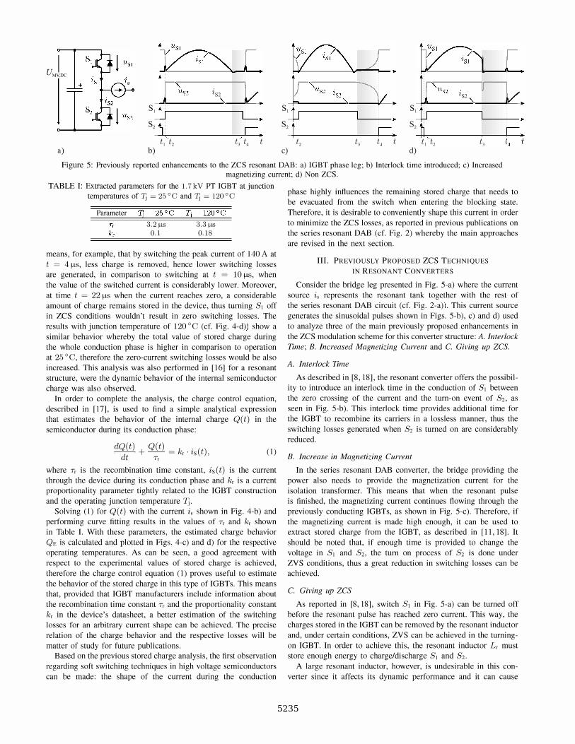
I UMV,DC
+
150 75
� U 100 50 2.
C Q) Q) � t:: 50 25 = ..c U U
0 0
c)
150 75
� 100 ..... 50 U 2.
c Q) Q) 2!l .... .... 50 25 0; = ..c U U
0 0 0 5 10 15 20 25
�T [!-Is] d)
Figure 4: In order to measure the semiconductor's stored charge, the circuit in a) was used. The triangular current shape shown in b) is
generated by the current source is in a) and is used to measured stored charge in 1. 7 kV IGBTs for c) 25°C and d) 120°C junction
temperature.
II. SEMICONDUCTOR STORED CHARGE DYNAMICS
High voltage bipolar semiconductor devices, as previously men
tioned, store large amounts of charge during their conduction
phases. This charge, if not allowed to recombine internally, is
translated into switching losses when the device is taken back to
the blocking state. Since this stored charge is directly related to
the dissipated energy during the switching process, it is useful to
analyze the behavior of the charge Q stored in the switch during
its conduction phase.
Consider the circuit depicted in Fig. 4-a) where an IGBT
based bridge leg is presented. Here, a current source generates the
triangular current is shown in Fig. 3-b) whereby switch 81 is turned
on at t = 0, the beginning of the switching period, and turned-off
at t = 6.T. By increasing stepwise the value of 6.T from 6.T = 0
to 6.T = toft, the current turned-off by device 81 is modified,
as shown in Fig. 4-b). Measuring the current iSI through 81 and
integrating it during the switching process for each value of 6.T, the charge stored in the device during the conduction phase can be
constructed.
This experiment was performed on a bridge leg based on 1.7kV PT IGBTs (FFlS0R17KE4) operating at 20 kHz with a DC-link
voltage of UMV.DC = 1 kV and reaching a peak current of 140 A. The results for the behavior of the charge Q for junction tem
peratures of 25 ° C and 120 ° C are presented in Figs. 4-c) and d)
respectively.
From Fig. 4-c) it can be seen that the stored charge Q is not
proportional to the conducted current, therefore it can be already
concluded that switching losses under these conditions do not
depend on the instantaneous value of the switched current. This
5234
I U"" �� L. � J0?�_[, �) UMV,DC
jp" ts iS2 !Is ZS2 � �
s, t s, t
s, t I I I S2 � c: :;lC.
S2 t C. S2 ... Pc: t, t2 t3 t4 t t2 t3 t. t t, t2 t3
[,
C. a) b) c) d)
Figure 5: Previously reported enhancements to the ZCS resonant DAB: a) IGBT phase leg; b) Interlock time introduced; c) Increased magnetizing current; d) Non ZCS.
TABLE I: Extracted parameters for the 1. 7 kV PT IGBT at junction
temperatures of 7J = 25 ° C and 7J = 120 ° C
Parameter
3.2 !lS 0. 1
3.3 !lS 0. 18
means, for example, that by switching the peak current of 140 A at
t = 4 J.l.S, less charge is removed, hence lower switching losses
are generated, in comparison to switching at t = 10 J.l.S, when
the value of the switched current is considerably lower. Moreover,
at time t = 22 J.l.S when the current reaches zero, a considerable
amount of charge remains stored in the device, thus turning 51 off
in ZCS conditions wouldn't result in zero switching losses. The
results with junction temperature of 1200e (cf. Fig. 4-d) show a
similar behavior whereby the total value of stored charge during
the whole conduction phase is higher in comparison to operation
at 25 °e, therefore the zero-current switching losses would be also
increased. This analysis was also performed in [16] for a resonant
structure, were the dynamic behavior of the internal semiconductor
charge was also observed.
In order to complete the analysis, the charge control equation,
described in [17], is used to find a simple analytical expression
that estimates the behavior of the internal charge Q(t) in the
semiconductor during its conduction phase:
dQ(t) + Q(t) = kr . is(t),
dt Tr (1)
where Tr is the recombination time constant, is(t) is the current
through the device during its conduction phase and kr is a current
proportionality parameter tightly related to the IGBT construction
and the operating junction temperature 1]. Solving (1) for Q(t) with the current is shown in Fig. 4-b) and
performing curve fitting results in the values of Tr and kr shown
in Table I. With these parameters, the estimated charge behavior
QE is calculated and plotted in Figs. 4-c) and d) for the respective
operating temperatures. As can be seen, a good agreement with
respect to the experimental values of stored charge is achieved,
therefore the charge control equation (1) proves useful to estimate
the behavior of the stored charge in this type of IGBTs. This means
that, provided that IGBT manufacturers include information about
the recombination time constant Tr and the proportionality constant
kr in the device's data sheet, a better estimation of the switching
losses for an arbitrary current shape can be achieved. The precise
relation of the charge behavior and the respective losses will be
matter of study for future publications.
Based on the previous stored charge analysis, the first observation
regarding soft switching techniques in high voltage semiconductors
can be made: the shape of the current during the conduction
phase highly influences the remaining stored charge that needs to
be evacuated from the switch when entering the blocking state.
Therefore, it is desirable to conveniently shape this current in order
to minimize the ZCS losses, as reported in previous publications on
the series resonant DAB (cf. Fig. 2) whereby the main approaches
are revised in the next section.
III. PREVIOUSLY PROPOSED ZCS TECHNIQUES IN RESONANT CONVERTERS
Consider the bridge leg presented in Fig. 5-a) where the current
source is represents the resonant tank together with the rest of
the series resonant DAB circuit (cf. Fig. 2-a». This current source
generates the sinusoidal pulses shown in Figs. 5-b), c) and d) used
to analyze three of the main previously proposed enhancements in
the ZCS modulation scheme for this converter structure: A. Interlock
Time; B. Increased Magnetizing Current and C. Giving up ZCS.
A. Interlock Time
As described in [8,18], the resonant converter offers the possibil
ity to introduce an interlock time in the conduction of 51 between
the zero crossing of the current and the turn-on event of 52, as
seen in Fig. 5-b). This interlock time provides additional time for
the IGBT to recombine its carriers in a lossless manner, thus the
switching losses generated when 52 is turned on are considerably
reduced.
B. Increase in Magnetizing Current
In the series resonant DAB converter, the bridge providing the
power also needs to provide the magnetization current for the
isolation transformer. This means that when the resonant pulse
is finished, the magnetizing current continues flowing through the
previously conducting IGBTs, as shown in Fig. 5-c). Therefore, if
the magnetizing current is made high enough, it can be used to
extract stored charge from the IGBT, as described in [11,18]. It
should be noted that, if enough time is provided to change the
voltage in 51 and 52, the turn on process of 52 is done under
ZVS conditions, thus a great reduction in switching losses can be
achieved.
C. Giving up ZCS
As reported in [8,18], switch 51 in Fig. 5-a) can be turned off
before the resonant pulse has reached zero current. This way, the
charges stored in the IGBT can be removed by the resonant inductor
and, under certain conditions, ZVS can be achieved in the turning
on IGBT. In order to achieve this, the resonant inductor Lr must
store enough energy to charge/discharge 51 and 52. A large resonant inductor, however, is undesirable in this con
verter since it affects its dynamic performance and it can cause
5235
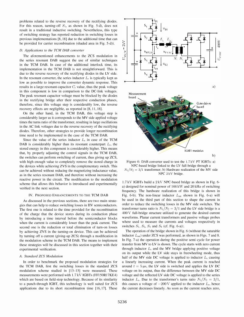
problems related to the reverse recovery of the rectifying diodes.
For this reason, turning-off 81, as shown in Fig. 5-d), does not
result in a traditional inductive switching. Nevertheless, this type
of switching strategy has reported reduction in switching losses in
previous implementations [8,18] due to the additional time that can
be provided for carrier recombination (shaded area in Fig. 5-d».
D. Applications to the TCM DAB converter
The aforementioned enhancements to the ZCS modulation in
the series resonant DAB suggest the use of similar techniques
in the TCM DAB. In case of the additional interlock time, its
implementation in the TCM DAB is not straightforward. This is
due to the reverse recovery of the rectifying diodes in the LV side.
In the resonant converter, the series inductor Lr is typically kept as
low as possible to improve the converter dynamic response. This
results in a large resonant capacitor Cr value, thus the peak voltage
in this component is low in comparison to the DC-link voltages.
The peak resonant capacitor voltage must be blocked by the diodes
in the rectifying bridge after their respective conduction phases,
therefore, since this voltage step is considerably low, the reverse
recovery effects are negligible, as reported in [8,11,18].
On the other hand, in the TCM DAB, this voltage step is
considerably larger as it corresponds to the MV side applied voltage
times the turns ratio of the transformer, resulting in large oscillations
in the AC link voltages due to the reverse recovery of the rectifying
diodes. Therefore, other strategies to provide longer recombination
time need to be implemented in the case of the TCM DAB.
Since the value of the series inductor Ls in case of the TCM
DAB is considerably higher than its resonant counterpart Lr, the
stored energy in this component is considerably higher. This means
that, by properly adjusting the control signals in the TCM DAB,
the switches can perform switching of current, thus giving up ZCS,
with high enough value to completely remove the stored charge in
the devices while achieving ZVS in the complementary switch. This
can be achieved without reducing the magnetizing inductance value,
as in the series resonant DAB, and therefore without increasing the
reactive power in the circuit. The modification to the modulation
scheme that allows this behavior is introduced and experimentally
verified in the next section.
IV. PROPOSED ENHANCEMENTS TO THE TCM DAB
As discussed in the previous sections, there are two main strate
gies that can help to reduce switching losses in HV semiconductors.
The first one is related to the time provided for the recombination
of the charge that the device stores during its conduction phase
by introducing a time interval before the semiconductor blocks
when the current is considerably lower than the peak current. The
second one is the reduction or total elimination of turn-on losses
by achieving ZVS in the turning-on device. This can be achieved
by turning off a current (giving-up ZCS) through a modification in
the modulation scheme in the TCM DAB. The means to implement
these strategies will be discussed in this section together with their
experimental verification.
A. Standard ZCS Modulation
In order to benchmark the proposed modulation strategies for
the TCM DAB, first the switching losses in the standard ZCS
modulation scheme studied in [13-15] were measured. These
measurements were performed with 1.7 kV IGBTs (FFI50RI7KE4)
which are based on field-stop technology. Because of its similarity
to a punch-through IGBT, this technology is well suited for ZCS
applications due to its short recombination time [16,17]. These
a)
Measurement board
b) Figure 6: DAB converter used to test the 1. 7 kV PT IGBTs: a)
NPC-based bridge linked to the LV full-bridge through a N, /N2 = 3/1 transformer; b) Hardware realization of the MV side
NPC 2 kV bridge.
1.7kV IGBTs build a 2kV NPC-based bridge as shown in Fig. 6-
a) designed for nominal power of 166 kW and 20 kHz of switching
frequency. The hardware realization of this bridge is shown in
Fig. 6-b). The non-linear inductor Lsat shown in Fig. 6-a) will
be used in the third part of this section to shape the current in
order to reduce the switching losses in the MV side switches. The
transformer turns ratio is N, / N2 = 3/1 and the LV side bridge is a
400 V full-bridge structure utilized to generate the desired current
waveforms. Planar current transformers and passive voltage probes
where used to measure the currents and voltages respectively in
switches 8" 82, 83 and 84 (cf. Fig. 6-a».
The operation of the bridge shown in Fig. 6 (without the saturable
inductor L,a,) under ZCS was performed, as shown in Figs. 7 and 8.
In Fig. 7-a) the operation during the positive semi cycle for power
transfer from MV to LV is shown. The cycle starts with zero current
through inductor Ls and the MV bridge applying positive voltage
on its output while the LV side stays in freewheeling mode, thus
half of the MV side DC voltage is applied to inductor L, causing
a linearly increasing current. When the peak current is reached
around t = 5 flS, the LV side is switched and applies the LV DC
voltage on its output, thus the difference between the MV side DC
voltage and the reflected LV side DC voltage is applied to the series
inductor Ls. Due to the transformer's turns ratio N,/N2 = 3/1,
this causes a voltage of - 200 V applied to the inductor L" hence
the current decreases linearly. As soon as the current reaches zero,
5236
1600 ,-----,------,------,------,,---,, : : :
o
-----� ••••••••• -,?--]� S I turn-off I S3 tUrn-on :
1 200 >' � 800 H·················· ·'i � 5 400 �
-400 '----------'-------'----------'--------'--'---------'------' o 5 a)
10 15 Time [I-ls]
20 25
1400 r---r---r-------, r---r--------,r-------, 1200
:> 1000 � 800 '" F 600 - 400 � 200
o J,.-:W._ .. __ .. '-_" ·'-"""!---ool
800
600 �
400 ';:: c Q) 200 .... .... ::: U
0
- 200
140 120 100 � 80 60 0: 40 � ::: 20 U 0
-2000
'----1'---------'
2'---------'
f20
b) c) Time [I-ls]
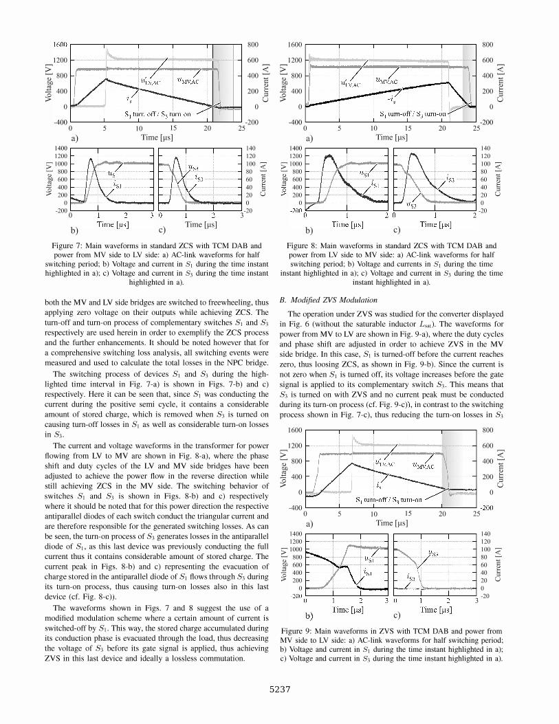
Figure 7: Main waveforms in standard ZCS with TCM DAB and power from MV side to LV side: a) AC-link waveforms for half
switching period; b) Voltage and current in SI during the time instant highlighted in a); c) Voltage and current in S3 during the time instant
highlighted in a).
both the MV and LV side bridges are switched to freewheeling, thus
applying zero voltage on their outputs while achieving ZCS. The
turn-off and turn-on process of complementary switches S, and S3 respectively are used herein in order to exemplify the ZCS process
and the further enhancements. It should be noted however that for
a comprehensive switching loss analysis, all switching events were
measured and used to calculate the total losses in the NPC bridge.
The switching process of devices S, and S3 during the high
lighted time interval in Fig. 7-a) is shown in Figs. 7-b) and c)
respectively. Here it can be seen that, since S, was conducting the
current during the positive semi cycle, it contains a considerable
amount of stored charge, which is removed when S3 is turned on
causing turn-off losses in SI as well as considerable turn-on losses
in S3.
The current and voltage waveforms in the transformer for power
flowing from LV to MV are shown in Fig. 8-a), where the phase
shift and duty cycles of the LV and MV side bridges have been
adjusted to achieve the power flow in the reverse direction while
still achieving ZCS in the MV side. The switching behavior of
switches S, and S3 is shown in Figs. 8-b) and c) respectively
where it should be noted that for this power direction the respective
anti parallel diodes of each switch conduct the triangular current and
are therefore responsible for the generated switching losses. As can
be seen, the turn-on process of S3 generates losses in the anti parallel
diode of SI, as this last device was previously conducting the full
current thus it contains considerable amount of stored charge. The
current peak in Figs. 8-b) and c) representing the evacuation of
charge stored in the antiparallel diode of S, flows through S3 during
its turn-on process, thus causing turn-on losses also in this last
device (cf. Fig. 8-c».
The waveforms shown in Figs. 7 and 8 suggest the use of a
modified modulation scheme where a certain amount of current is
switched-off by St. This way, the stored charge accumulated during
its conduction phase is evacuated through the load, thus decreasing
the voltage of S3 before its gate signal is applied, thus achieving
ZVS in this last device and ideally a lossless commutation.
1600
1 200 >' '";:;"' 800 0/) 5 400 �
0
800
600 �
400 �
C Q) 200 g
U o
-400 '---------'-----------'---------'---------'------'-------' - 200 o 5 10 15 20 25 a) Time [I-ls]
1400 r------.--------, r------.------, 140 1200
:> 1000 � 800 <l) F 600 :2 400 .,- 200
o
b) c)
120 100 � 80 60 0: 40 � ::: 20 U 0
2 -20
Figure 8: Main waveforms in standard ZCS with TCM DAB and power from LV side to MV side: a) AC-link waveforms for half switching period; b) Voltage and currents in SI during the time
instant highlighted in a); c) Voltage and current in S3 during the time instant highlighted in a).
B. Modified ZVS Modulation
The operation under ZVS was studied for the converter displayed
in Fig. 6 (without the saturable inductor Lsa,). The waveforms for
power from MV to LV are shown in Fig. 9-a), where the duty cycles
and phase shift are adjusted in order to achieve ZVS in the MV
side bridge. In this case, S, is turned-off before the current reaches
zero, thus loosing ZCS, as shown in Fig. 9-b). Since the current is
not zero when SI is turned off, its voltage increases before the gate
signal is applied to its complementary switch S3. This means that
S3 is turned on with ZVS and no current peak must be conducted
during its turn-on process (cf. Fig. 9-c», in contrast to the switching
process shown in Fig. 7-c), thus reducing the turn-on losses in S3
1600
1 200 >' '";:;"' 800 0/) 5 400 �
0
-400
1400 1200
:> 1000 � 800 '" OJ) 600 Zl 400 � 200
0
800
600 �
400 �
C Q) 200 g
U o
'---------'-----------'---------'---------'-----'-------' - 200 0 5 a)
10 15 Time [I-ls]
� '$LS3
20
: ai/._ ... _ .... _ ... _ ... -i ..
25
140 120 100 80 ... _ ........ _.- 60 ... _ ... _ ... __ .- 40 ... _ ........ _.- 20 0
.. ... S3 � . ...... --..... -- ; .. r-L= ---�-""""--l
3 -20
c)
� 0: " � U
Figure 9: Main waveforms in ZVS with TCM DAB and power from MV side to LV side: a) AC-link waveforms for half switching period; b) Voltage and current in SI during the time instant highlighted in a); c) Voltage and current in S3 during the time instant highlighted in a),
5237
1600 800
1 200 600 >' :? '";:;"' 800 0/) 5 400 �
400 '::' C <l)
200 t: � u 0 0
-400 - 200 0 5 10 15 20 25 a) Time [J..ls]
1400 140 1200 120
:> 1000 � 800 <l) OJ) 600 $3 400 � 200
100 � 80 I: 60 <l)
40 g 20 U
0 0 -200
0 I I 2 -20
b) Time [Ils] c)
Time [Ils]
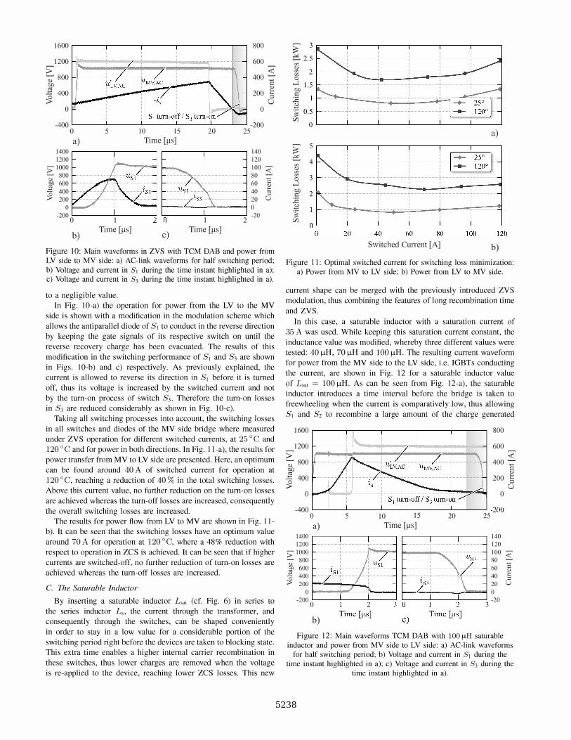
Figure 10: Main waveforms in ZVS with TCM DAB and power from LV side to MV side: a) AC-link waveforms for half switching period; b) Voltage and current in 31 during the time instant highlighted in a); c) Voltage and current in 33 during the time instant highlighted in a).
to a negligible value.
In Fig. lO-a) the operation for power from the LV to the MV
side is shown with a modification in the modulation scheme which
allows the antiparallel diode of S, to conduct in the reverse direction
by keeping the gate signals of its respective switch on until the
reverse recovery charge has been evacuated. The results of this
modification in the switching performance of SI and S3 are shown
in Figs. lO-b) and c) respectively. As previously explained, the
current is allowed to reverse its direction in SI before it is turned
off, thus its voltage is increased by the switched current and not
by the turn-on process of switch S3. Therefore the turn-on losses
in S3 are reduced considerably as shown in Fig. lO-c).
Taking all switching processes into account, the switching losses
in all switches and diodes of the MV side bridge where measured
under ZVS operation for different switched currents, at 25°C and
120°C and for power in both directions. In Fig. II-a), the results for
power transfer from MV to LV side are presented. Here, an optimum
can be found around 40 A of switched current for operation at
120 ° C, reaching a reduction of 40 % in the total switching losses.
Above this current value, no further reduction on the turn-on losses
are achieved whereas the turn-off losses are increased, consequently
the overall switching losses are increased.
The results for power flow from LV to MV are shown in Fig. lI
b). It can be seen that the switching losses have an optimum value
around 70 A for operation at 120°C, where a 48% reduction with
respect to operation in ZCS is achieved. It can be seen that if higher
currents are switched-off, no further reduction of turn-on losses are
achieved whereas the turn-off losses are increased.
C. The Saturable Inductor
By inserting a saturable inductor Lsat (cf. Fig. 6) in series to
the series inductor Ls, the current through the transformer, and
consequently through the switches, can be shaped conveniently
in order to stay in a low value for a considerable portion of the
switching period right before the devices are taken to blocking state.
This extra time enables a higher internal carrier recombination in
these switches, thus lower charges are removed when the voltage
is re-applied to the device, reaching lower ZCS losses. This new
� 3
� 2.5 </> <l)
2 </> en 0 .....l 1.5 0/)
. :: ..c B .� 0.5 VJ
0 a)
� 5
� 4 en <l) </> en 3 0 .....l 0/) 2 c :.c B .� VJ
Switched Current [A] b) Figure 11: Optimal switched current for switching loss minimization:
a) Power from MV to LV side; b) Power from LV to MV side.
current shape can be merged with the previously introduced ZVS
modulation, thus combining the features of long recombination time
and ZVS.
In this case, a saturable inductor with a saturation current of
35 A was used. While keeping this saturation current constant, the
inductance value was modified, whereby three different values were
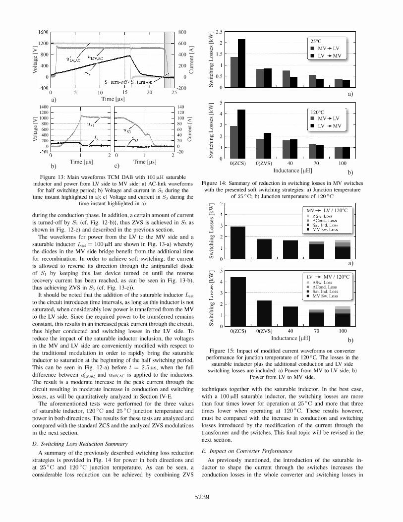
tested: 40 J..lH, 70 J..lH and 100 J..lH. The resulting current waveform
for power from the MV side to the LV side, i.e. IGBTs conducting
the current, are shown in Fig. 12 for a saturable inductor value
of Lsat = 100 J..lH. As can be seen from Fig. 12-a), the saturable
inductor introduces a time interval before the bridge is taken to
freewheeling when the current is comparatively low, thus allowing
S, and S2 to recombine a large amount of the charge generated
1600
1 200 >' '";:;"' 800 0/) �
.=: 400 � 0
800
600 :?
400 � C <l) 200 �
U o
-400 ��--�------�----�------��--� - 200 0 a)
1400 1200
:> 1000 � 800 0,) OJ) 600 $3 400 � 200
0 -200
0
b)
5 to 15 Time [Ils]
20 25
140 120 100 � 80 60 I: 0,) 40 t:: ;:I 20 U 0
3 -20
Figure 12: Main waveforms TCM DAB with 100 J..lH saturable inductor and power from MV side to LV side: a) AC-link waveforms
for half switching period; b) Voltage and current in 3, during the time instant highlighted in a); c) Voltage and current in 33 during the
time instant highlighted in a).
5238
1600 ,-----,------,------,------,---,-, 1200
>' � 800 � 5 400 �
o
_400 L------L------L-----�------�--�� o 5 a)
10 15 Time [J..ls]
1400 ,-------,-----,
20 25
1200 :> 1000 � 800 <l) � 600 � 400
::·�·:/ . . v ........................... -i S3 20� I=-:?ioo""'�-/,� _ _l
b) I
Time [J..ls]
2 0
c)
ZiS3 I
Time [J..ls]
2
800
600 :? 400 '::' c (l)
200 g U
0
-200
140 120 100 � 80 60 I: (l) 40 g 20 U 0 -20
Figure 13: Main waveforms TCM DAB with lOOI1H saturable inductor and power from LV side to MV side: a) AC-link waveforms
for half switching period; b) Voltage and current in 31 during the time instant highlighted in a); c) Voltage and current in 33 during the
time instant highlighted in a).
during the conduction phase. In addition, a certain amount of current
is turned-off by 51 (cf. Fig. 12-b», thus ZVS is achieved in 53 as
shown in Fig. 12-c) and described in the previous section.
The waveforms for power from the LV to the MV side and a
saturable inductor Lsat = lOOI1H are shown in Fig. 13-a) whereby
the diodes in the MV side bridge benefit from the additional time
for recombination. In order to achieve soft switching, the current
is allowed to reverse its direction through the antiparallel diode
of 51 by keeping this last device turned on until the reverse
recovery current has been reached, as can be seen in Fig. 13-b),
thus achieving ZVS in 53 (cf. Fig. 13-c».
It should be noted that the addition of the saturable inductor Lsat to the circuit introduces time intervals, as long as this inductor is not
saturated, when considerably low power is transferred from the MV
to the LV side. Since the required power to be transferred remains
constant, this results in an increased peak current through the circuit,
thus higher conducted and switching losses in the LV side. To
reduce the impact of the saturable inductor inclusion, the voltages
in the MV and LV side are conveniently modified with respect to
the traditional modulation in order to rapidly bring the saturable
inductor to saturation at the beginning of the half switching period.
This can be seen in Fig. 12-a) before t = 2.5 flS, when the full
difference between U�V.AC and UMV,AC is applied to the inductors.
The result is a moderate increase in the peak current through the
circuit resulting in moderate increase in conduction and switching
losses, as will be quantitatively analyzed in Section IV-E.
The aforementioned tests were performed for the three values
of saturable inductor, 120°C and 25°C junction temperature and
power in both directions. The results for these tests are analyzed and
compared with the standard ZCS and the analyzed ZVS modulations
in the next section.
D. Switching Loss Reduction Summary
A summary of the previously described switching loss reduction
strategies is provided in Fig. 14 for power in both directions and
at 25°C and 120°C junction temperature. As can be seen, a
considerable loss reduction can be achieved by combining ZVS
::: 2.5
=. 2 '" (l) � 1.5 ....:I 0/) c :.a .g 0.5 � [/J 0
::: 5
=. 4 '" (l) '" 3 '" 0 ....:I 0/) 2 c :.a B .� [/J 0
O(ZcS) O(ZVS)
25°C • MV-+-LV • LV -+-MV
a)
120°C • MV-+-LV • LV -+-MV
40 70 \00 Inductance [J..lH] b)
Figure 14: Summary of reduction in switching losses in MV switches with the presented soft switching strategies: a) Junction temperature
of 25°C; b) Junction temperature of 120°C 5�------------�========� � 41-.... · ...... · ...... ··· ...... · ...... ·· ........ · ...... · ...... ··· ...... · ...... · .... 1
'" (l) � 31-.. ·:��� .......... ·· ............ · ...... · ............ ·· ............ ·1 ....:I � 2
:.a B .� [/J o
MV -+ LV I 120°C
a) � 5�--------------�========� ;;> LV -+ MV I 120°C =. 4 • ,,",Sw. Loss
3
0/) 2 .:: ..c B .� [/J o
O(ZcS)
• ,,",Cond. Loss • Sat. Ind. Loss • MV Sw. Loss
O(ZVS) 40 70 Inductance [J..lH]
100 b)
Figure 15: Impact of modified current waveforms on converter performance for junction temperature of 120°C. The losses in the
saturable inductor plus the additional conduction and LV side switching losses are included: a) Power from MV to LV side; b)
Power from LV to MV side.
techniques together with the saturable inductor. In the best case,
with a lOOI1H saturable inductor, the switching losses are more
than four times lower for operation at 25°C and more that three
times lower when operating at 120°C. These results however,
must be compared with the increase in conduction and switching
losses introduced by the modification of the current through the
transformer and the switches. This final topic will be revised in the
next section.
E. Impact on Converter Performance
As previously mentioned, the introduction of the saturable in
ductor to shape the current through the switches increases the
conduction losses in the whole converter and switching losses in
5239
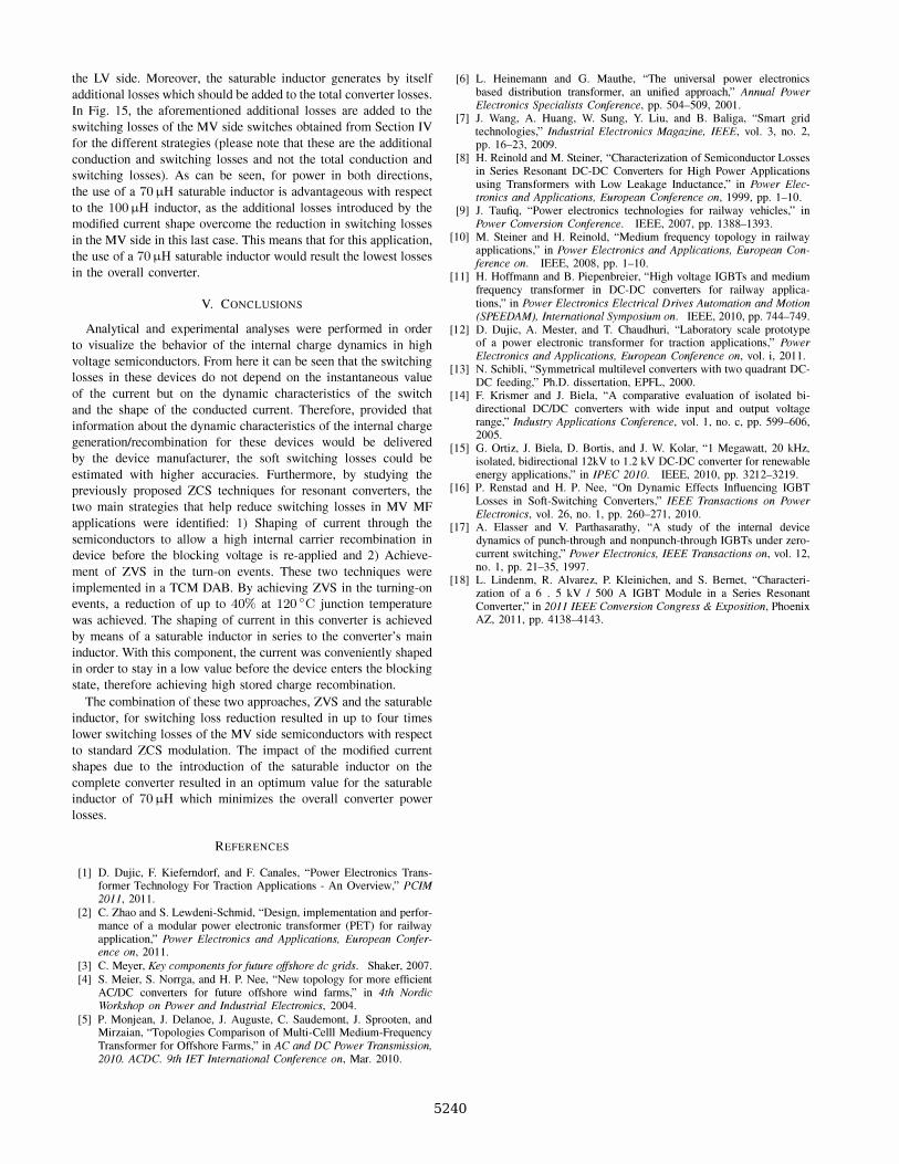
the LY side. Moreover, the saturable inductor generates by itself
additional losses which should be added to the total converter losses.
In Fig. 15, the aforementioned additional losses are added to the
switching losses of the MY side switches obtained from Section IY
for the different strategies (please note that these are the additional
conduction and switching losses and not the total conduction and
switching losses). As can be seen, for power in both directions,
the use of a 70 J.1.H saturable inductor is advantageous with respect
to the 100 J.1.H inductor, as the additional losses introduced by the
modified current shape overcome the reduction in switching losses
in the MY side in this last case. This means that for this application,
the use of a 70 J.1.H saturable inductor would result the lowest losses
in the overall converter.
Y. CONCLUSIONS
Analytical and experimental analyses were performed in order
to visualize the behavior of the internal charge dynamics in high
voltage semiconductors. From here it can be seen that the switching
losses in these devices do not depend on the instantaneous value
of the current but on the dynamic characteristics of the switch
and the shape of the conducted current. Therefore, provided that
information about the dynamic characteristics of the internal charge
generation/recombination for these devices would be delivered
by the device manufacturer, the soft switching losses could be
estimated with higher accuracies. Furthermore, by studying the
previously proposed ZCS techniques for resonant converters, the
two main strategies that help reduce switching losses in MY MF
applications were identified: 1) Shaping of current through the
semiconductors to allow a high internal carrier recombination in
device before the blocking voltage is re-applied and 2) Achieve
ment of ZYS in the turn-on events. These two techniques were
implemented in a TCM DAB. By achieving ZYS in the turning-on
events, a reduction of up to 40% at 120°C junction temperature
was achieved. The shaping of current in this converter is achieved
by means of a saturable inductor in series to the converter's main
inductor. With this component, the current was conveniently shaped
in order to stay in a low value before the device enters the blocking
state, therefore achieving high stored charge recombination.
The combination of these two approaches, ZYS and the saturable
inductor, for switching loss reduction resulted in up to four times
lower switching losses of the MY side semiconductors with respect
to standard ZCS modulation. The impact of the modified current
shapes due to the introduction of the saturable inductor on the
complete converter resulted in an optimum value for the saturable
inductor of 70 J.1.H which minimizes the overall converter power
losses.
REFERENCES
[ 1] D. Dujic, F. Kieferndorf, and F. Canales, "Power Electronics Transformer Technology For Traction Applications - An Overview," P CIM 2011, 20 1 1.
[ 2] C. Zhao and S. Lewdeni-Schmid, "Design, implementation and performance of a modular power electronic transformer (PET) for railway application," Power Electronics and Applications, European Conference on, 20 1 1.
[3] c. Meyer, Key components for future offshore dc grids. Shaker, 200 7. [4] S. Meier, S. Norrga, and H. P. Nee, "New topology for more efficient
ACIDC converters for future offshore wind farms," in 4th Nordic Workshop on Power and Industrial Electronics, 2004.
[5] P. Monjean, J. Delanoe, J. Auguste, C. Saudemont, J. Sprooten, and Mirzaian, "Topologies Comparison of Multi-Celll Medium-Frequency Transformer for Offshore Farms," in AC and DC Power Transmission, 2010. ACDC. 9th lET International Conference on, Mar. 20 10.
[6] L. Heinemann and G. Mauthe, "The universal power electronics based distribution transformer, an unified approach," Annual Power Electronics Specialists Conference, pp. 504-509, 200 1.
[ 7] J. Wang, A. Huang, W. Sung, Y. Liu, and B. Baliga, "Smart grid technologies," Industrial Electronics Magazine, IEEE, vol. 3, no. 2, pp. 16- 23, 2009.
[ 8] H. Reinold and M. Steiner, "Characterization of Semiconductor Losses in Series Resonant DC-DC Converters for High Power Applications using Transformers with Low Leakage Inductance," in Power Electronics and Applications, European Conference on, 1999, pp. 1- 10.
[9] J. Taufiq, "Power electronics technologies for railway vehicles," in Power Conversion Conference. IEEE, 200 7, pp. 13 8 8- 1393.
[ 10] M. Steiner and H. Reinold, "Medium frequency topology in railway applications," in Power Electronics and Applications, European Conference on. IEEE, 200 8, pp. 1- 10.
[ 1 1] H. Hoffmann and B. Piepenbreier, "High voltage IGBTs and medium frequency transformer in DC-DC converters for railway applications," in Power Electronics Electrical Drives Automation and Motion (SPEEDAM), International Symposium on. IEEE, 20 10, pp. 744- 749.
[ 1 2] D. Dujic, A. Mester, and T. Chaudhuri, "Laboratory scale prototype of a power electronic transformer for traction applications," Power Electronics and Applications, European Conference on, vol. i, 20 1 1.
[ 13] N. Schibli, "Symmetrical multilevel converters with two quadrant DCDC feeding," Ph.D. dissertation, EPFL, 2000.
[ 14] F. Krismer and J. Biela, "A comparative evaluation of isolated bidirectional DCfDC converters with wide input and output voltage range," Industry Applications Conference, vol. 1, no. c, pp. 599-606, 2005.
[ 15] G. Ortiz, 1. Biela, D. Bortis, and J. W. Kolar, " 1 Megawatt, 20 kHz, isolated, bidirectional 1 2kY to 1. 2 kY DC-DC converter for renewable energy applications," in IP EC 2010. IEEE, 20 10, pp. 3 2 1 2-3 2 19.
[ 16] P. Renstad and H. P. Nee, "On Dynamic Effects Influencing IGBT Losses in Soft-Switching Converters," IEEE Transactions on Power Electronics, vol. 26, no. 1, pp. 260- 2 7 1, 20 10.
[ 1 7] A. Elasser and V. Parthasarathy, "A study of the internal device dynamics of punch-through and nonpunch-through IGBTs under zerocurrent switching," Power Electronics, IEEE Transactions on, vol. 1 2, no. 1, pp. 2 1-35, 199 7.
[ 1 8] L. Lindenm, R. Alvarez, P. Kleinichen, and S. Bernet, "Characterization of a 6 . 5 kY / 500 A IGBT Module in a Series Resonant Converter," in 201 llEEE Conversion Congress & Exposition, Phoenix AZ, 20 1 1, pp. 4 13 8-4 143.
5240