software defined radio handbook - ab4oj/va7oj's … · · 2015-11-27software defined radio...
TRANSCRIPT
PPPPPentek, Inc.entek, Inc.entek, Inc.entek, Inc.entek, Inc. • One Park Way, Upper Saddle River, NJ 07458 • Tel: (201) 818-5900 • Fax: (201) 818-5904 • Email: [email protected] • http://www.pentek.com
11111
SoSoSoSoSoffffftttttware Defined Rware Defined Rware Defined Rware Defined Rware Defined Radio Handbookadio Handbookadio Handbookadio Handbookadio Handbook10th Edition
PPPPPentek, Inc.entek, Inc.entek, Inc.entek, Inc.entek, Inc.One Park Way, Upper Saddle River, New Jersey 07458
Tel: (201) 818-5900 • Fax: (201) 818-5904Email: [email protected] • http://www.pentek.com
Copyright © 1998, 2001, 2003, 2006, 2008, 2009, 2010, 2011, 2012, 2013 Pentek, Inc.Last updated: April 2013
All rights reserved.Contents of this publication may not be reproduced in any form without written permission.
Specifications are subject to change without notice.Pentek, GateFlow, ReadyFow, SystemFlow and Cobalt are registered trademarks of Pentek, Inc.
SamplingSamplingSamplingSamplingSampling
PPPPPrinciples of SDRrinciples of SDRrinciples of SDRrinciples of SDRrinciples of SDR
TTTTTechnologyechnologyechnologyechnologyechnology
PPPPProductsroductsroductsroductsroducts
ApplicationsApplicationsApplicationsApplicationsApplications
LinksLinksLinksLinksLinks
by
RRRRRodger Hodger Hodger Hodger Hodger H. Hosking. Hosking. Hosking. Hosking. HoskingVice-President & Cofounder of Pentek, Inc.
®

PPPPPentek, Inc.entek, Inc.entek, Inc.entek, Inc.entek, Inc. • One Park Way, Upper Saddle River, NJ 07458 • Tel: (201) 818-5900 • Fax: (201) 818-5904 • Email: [email protected] • http://www.pentek.com
22222
Software Defined Radio Handbook
Preface
SDR (Software-Defined Radio) has revolutionized electronic systems for avariety of applications including communications, data acquisition and signal processing.
This handbook shows how DDCs (Digital Downconverters) and DUCs (Digital Upconverters),the fundamental building blocks of SDR, can replace legacy analog receiver and transmitter designs while
offering significant benefits in performance, density and cost.
In order to fully appreciate the benefits of SDR, conventional analog receiver and transmittersystems will be compared to their digital counterparts, highlighting similarities and differences.
The inner workings of the SDR will be explored with an in-depth description of the internalstructure and the devices used. Finally, some actual board- and system-level implementations and available
off-the-shelf SDR products and applications based on such products will be presented.
For more information on complementary subjects, the reader is referred to these Pentek Handbooks:Putting FPGAs to Work in Software Radio Systems
Critical Techniques for High-Speed A/D Converters in Real-Time SystemsHigh-Speed Switched Serial Fabrics Improve System Design
High-Speed, Real-Time Recording Systems
PPPPPentek, Inc.entek, Inc.entek, Inc.entek, Inc.entek, Inc. • One Park Way, Upper Saddle River, NJ 07458 • Tel: (201) 818-5900 • Fax: (201) 818-5904 • Email: [email protected] • http://www.pentek.com
33333
Software Defined Radio Handbook
Before we look at SDR and its various implementa-tions in embedded systems, we’ll review a theoremfundamental to sampled data systems such as thoseencountered in Software-Defined Radios.
Nyquist’s Theorem:
“Any signal can be represented by discretesamples if the sampling frequency is at least twice
the bandwidth of the signal.”
Notice that we highlighted the word bandwidthrather than frequency. In what follows, we’ll attempt toshow the implications of this theorem and the correctinterpretation of sampling frequency, also known assampling rate.
SamplingSamplingSamplingSamplingSampling
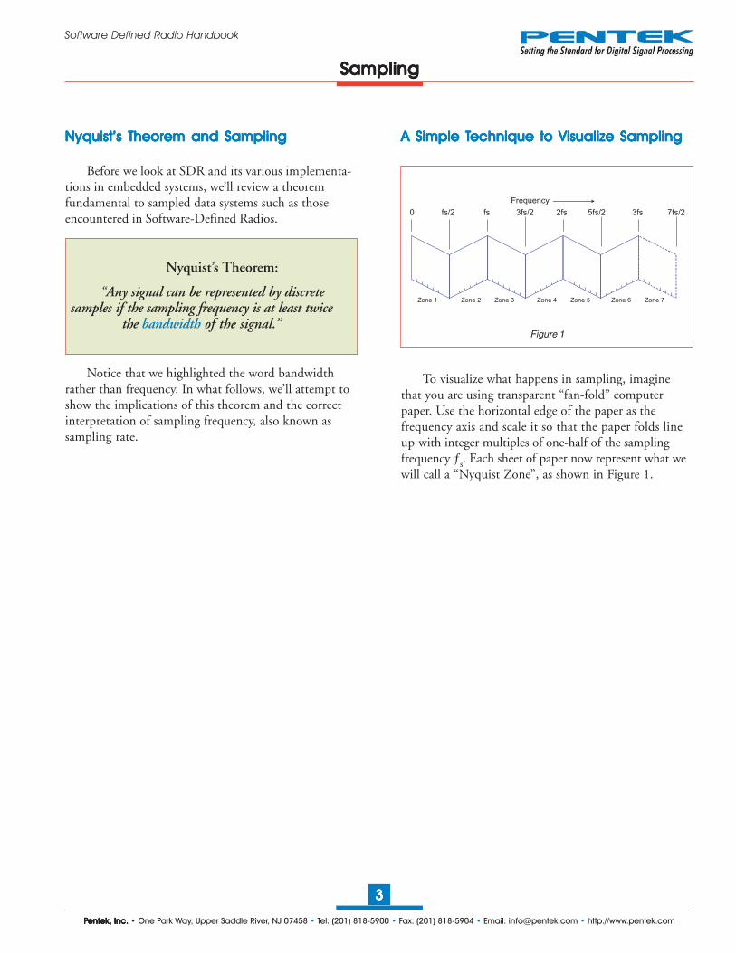
A Simple TA Simple TA Simple TA Simple TA Simple Technique to Visualize Samplingechnique to Visualize Samplingechnique to Visualize Samplingechnique to Visualize Samplingechnique to Visualize Sampling
To visualize what happens in sampling, imaginethat you are using transparent “fan-fold” computerpaper. Use the horizontal edge of the paper as thefrequency axis and scale it so that the paper folds lineup with integer multiples of one-half of the samplingfrequency ƒs. Each sheet of paper now represent what wewill call a “Nyquist Zone”, as shown in Figure 1.
Figure 1
Nyquist’s Theorem and SamplingNyquist’s Theorem and SamplingNyquist’s Theorem and SamplingNyquist’s Theorem and SamplingNyquist’s Theorem and Sampling
fs/2 fs 3fs/2 2fs 5fs/2 3fs 7fs/20
Zone 1 Zone 2 Zone 3 Zone 4 Zone 5 Zone 6 Zone 7
Frequency

PPPPPentek, Inc.entek, Inc.entek, Inc.entek, Inc.entek, Inc. • One Park Way, Upper Saddle River, NJ 07458 • Tel: (201) 818-5900 • Fax: (201) 818-5904 • Email: [email protected] • http://www.pentek.com
44444
Software Defined Radio Handbook
SamplingSamplingSamplingSamplingSampling
Figure 3
Baseband SamplingBaseband SamplingBaseband SamplingBaseband SamplingBaseband Sampling
Figure 4
A baseband signal has frequency components thatstart at ƒ = 0 and extend up to some maximum frequency.
To prevent data destruction when sampling a basebandsignal, make sure that all the signal energy falls ONLY inthe 1st Nyquist band, as shown in Figure 4.
There are two ways to do this:1. Insert a lowpass filter to eliminate all signals
above ƒs/2, or2. Increase the sampling frequency so all signals
present fall below ƒs/2.
Note that ƒs/2 is also known as the “folding frequency”.
Sampling Bandpass SignalsSampling Bandpass SignalsSampling Bandpass SignalsSampling Bandpass SignalsSampling Bandpass Signals
Figure 2
Use the vertical axis of the fan-fold paper for signalenergy and plot the frequency spectrum of the signal tobe sampled, as shown in Figure 2. To see the effects ofsampling, collapse the transparent fan-fold paper into astack.
Sampling BasicsSampling BasicsSampling BasicsSampling BasicsSampling Basics
The resulting spectrum can be seen by holding thetransparent stack up to a light and looking through it.You can see that signals on all of the sheets or zones are“folded” or “aliased” on top of each other — and theycan no longer be separated.
Once this folding or aliasing occurs during sampling,the resulting sampled data is corrupted and can never berecovered. The term “aliasing” is appropriate becauseafter sampling, a signal from one of the higher zonesnow appears to be at a different frequency.
Let’s consider bandpass signals like the IF frequencyof a communications receiver that might have a 70 MHzcenter frequency and 10 MHz bandwidth. In this case,the IF signal contains signal energery from 65 to 75 MHz.
If we follow the baseband sampling rules above, wemust sample this signal at twice the highest signalfrequency, meaning a sample rate of at least 150 MHz.
However, by taking advantage of a technique called“undersampling”, we can use a much lower sampling rate.
fs/2 fs 3fs/2 2fs 5fs/2 3fs 7fs/20
Zone 1 Zone 2 Zone 3 Zone 4 Zone 5 Zone 6 Zone 7
En
erg
y
fs/2 fs 3fs/2 2fs 5fs/2 3fs 7fs/20
Zone 1 Zone 2 Zone 3 Zone 4 Zone 5 Zone 6 Zone 7
No Signal Energy
fs/20Folded Signals
Fall On Top of
Each Other
PPPPPentek, Inc.entek, Inc.entek, Inc.entek, Inc.entek, Inc. • One Park Way, Upper Saddle River, NJ 07458 • Tel: (201) 818-5900 • Fax: (201) 818-5904 • Email: [email protected] • http://www.pentek.com
55555
Software Defined Radio Handbook
fs/20
Folded signals
still fall on top of
each other - but
now there is
energy in
only one sheet !
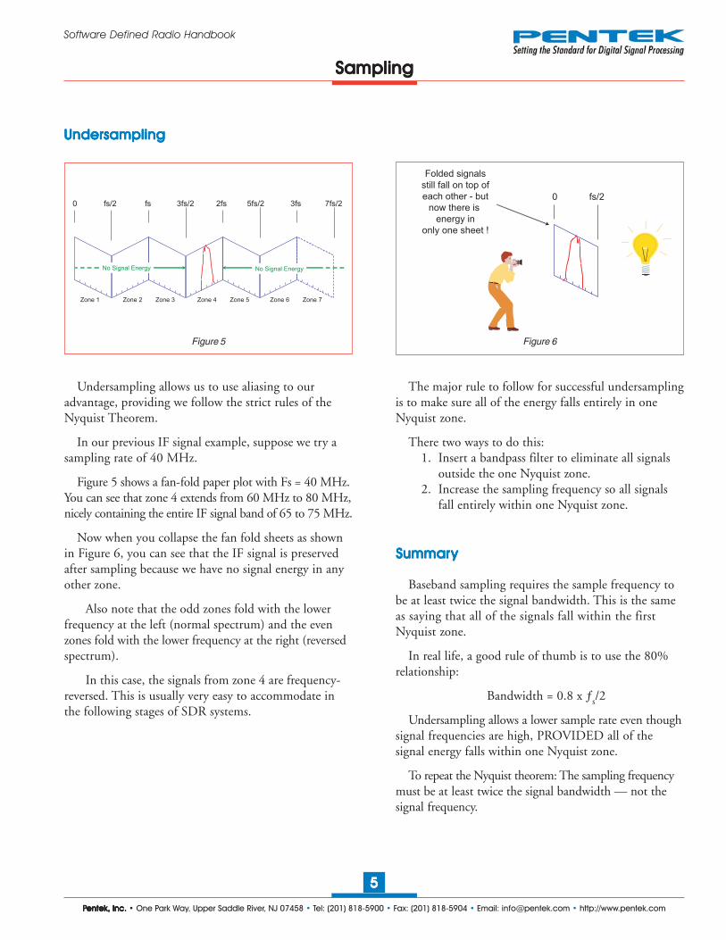
UndersamplingUndersamplingUndersamplingUndersamplingUndersampling
Figure 5
SamplingSamplingSamplingSamplingSampling
Figure 6
fs/2 fs 3fs/2 2fs 5fs/2 3fs 7fs/20
Zone 1 Zone 2 Zone 3 Zone 4 Zone 5 Zone 6 Zone 7
No Signal EnergyNo Signal Energy
Undersampling allows us to use aliasing to ouradvantage, providing we follow the strict rules of theNyquist Theorem.
In our previous IF signal example, suppose we try asampling rate of 40 MHz.
Figure 5 shows a fan-fold paper plot with Fs = 40 MHz.You can see that zone 4 extends from 60 MHz to 80 MHz,nicely containing the entire IF signal band of 65 to 75 MHz.
Now when you collapse the fan fold sheets as shownin Figure 6, you can see that the IF signal is preservedafter sampling because we have no signal energy in anyother zone.
Also note that the odd zones fold with the lowerfrequency at the left (normal spectrum) and the evenzones fold with the lower frequency at the right (reversedspectrum).
In this case, the signals from zone 4 are frequency-reversed. This is usually very easy to accommodate inthe following stages of SDR systems.
SummarSummarSummarSummarSummaryyyyy
Baseband sampling requires the sample frequency tobe at least twice the signal bandwidth. This is the sameas saying that all of the signals fall within the firstNyquist zone.
In real life, a good rule of thumb is to use the 80%relationship:
Bandwidth = 0.8 x ƒs/2
Undersampling allows a lower sample rate even thoughsignal frequencies are high, PROVIDED all of thesignal energy falls within one Nyquist zone.
To repeat the Nyquist theorem: The sampling frequencymust be at least twice the signal bandwidth — not thesignal frequency.
The major rule to follow for successful undersamplingis to make sure all of the energy falls entirely in oneNyquist zone.
There two ways to do this:1. Insert a bandpass filter to eliminate all signals
outside the one Nyquist zone.2. Increase the sampling frequency so all signals
fall entirely within one Nyquist zone.
PPPPPentek, Inc.entek, Inc.entek, Inc.entek, Inc.entek, Inc. • One Park Way, Upper Saddle River, NJ 07458 • Tel: (201) 818-5900 • Fax: (201) 818-5904 • Email: [email protected] • http://www.pentek.com
66666
Software Defined Radio Handbook
Figure 7
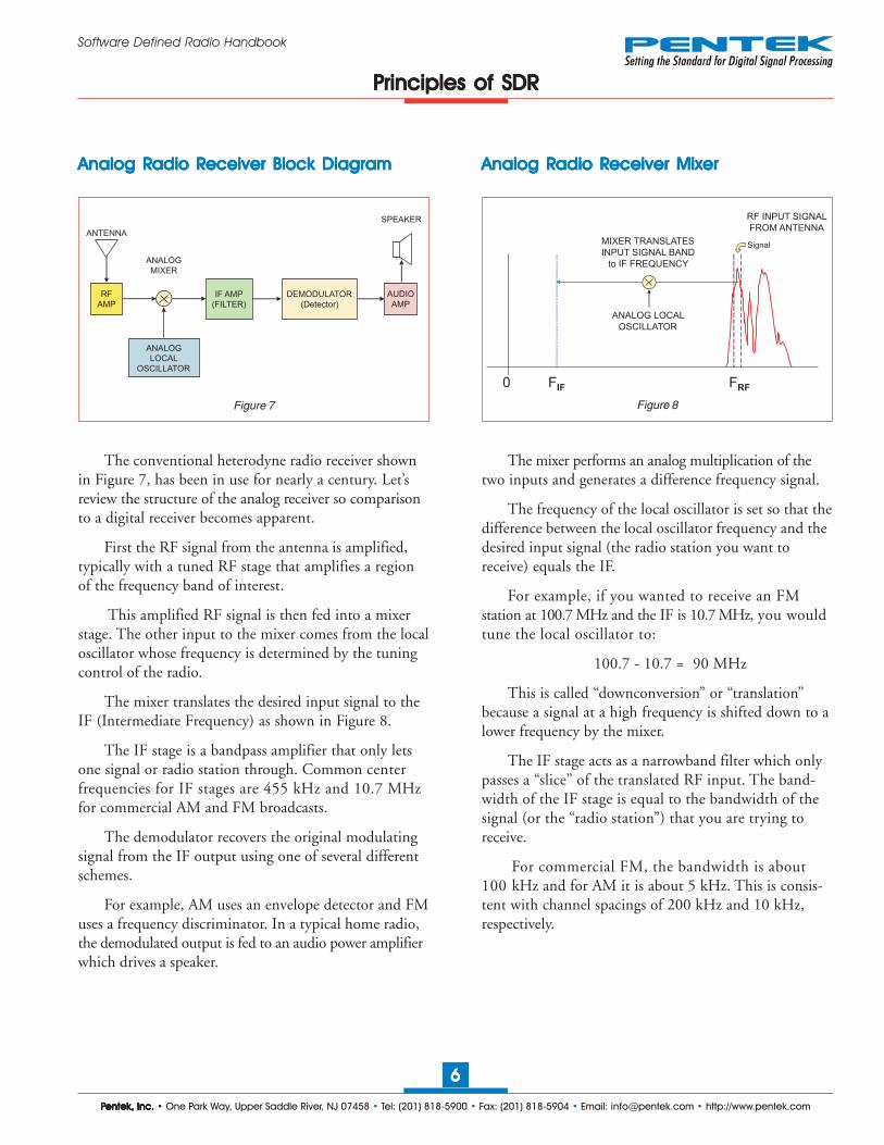
The conventional heterodyne radio receiver shownin Figure 7, has been in use for nearly a century. Let’sreview the structure of the analog receiver so comparisonto a digital receiver becomes apparent.
First the RF signal from the antenna is amplified,typically with a tuned RF stage that amplifies a regionof the frequency band of interest.
This amplified RF signal is then fed into a mixerstage. The other input to the mixer comes from the localoscillator whose frequency is determined by the tuningcontrol of the radio.
The mixer translates the desired input signal to theIF (Intermediate Frequency) as shown in Figure 8.
The IF stage is a bandpass amplifier that only letsone signal or radio station through. Common centerfrequencies for IF stages are 455 kHz and 10.7 MHzfor commercial AM and FM broadcasts.
The demodulator recovers the original modulatingsignal from the IF output using one of several differentschemes.
For example, AM uses an envelope detector and FMuses a frequency discriminator. In a typical home radio,the demodulated output is fed to an audio power amplifierwhich drives a speaker.
Figure 8
Analog RAnalog RAnalog RAnalog RAnalog Radio Radio Radio Radio Radio Receiver Block Diagrameceiver Block Diagrameceiver Block Diagrameceiver Block Diagrameceiver Block Diagram Analog RAnalog RAnalog RAnalog RAnalog Radio Radio Radio Radio Radio Receiver Mixereceiver Mixereceiver Mixereceiver Mixereceiver Mixer
The mixer performs an analog multiplication of thetwo inputs and generates a difference frequency signal.
The frequency of the local oscillator is set so that thedifference between the local oscillator frequency and thedesired input signal (the radio station you want toreceive) equals the IF.
For example, if you wanted to receive an FMstation at 100.7 MHz and the IF is 10.7 MHz, you wouldtune the local oscillator to:
100.7 - 10.7 = 90 MHz
This is called “downconversion” or “translation”because a signal at a high frequency is shifted down to alower frequency by the mixer.
The IF stage acts as a narrowband filter which onlypasses a “slice” of the translated RF input. The band-width of the IF stage is equal to the bandwidth of thesignal (or the “radio station”) that you are trying toreceive.
For commercial FM, the bandwidth is about100 kHz and for AM it is about 5 kHz. This is consis-tent with channel spacings of 200 kHz and 10 kHz,respectively.
PPPPPrinciples of SDRrinciples of SDRrinciples of SDRrinciples of SDRrinciples of SDR
ANALOG
LOCAL
OSCILLATOR
IF AMP
(FILTER)
SPEAKER
ANTENNA
DEMODULATOR
(Detector)
ANALOG
MIXER
AUDIO
AMP
RF
AMP
0
RF INPUT SIGNAL
FROM ANTENNA
MIXER TRANSLATES
INPUT SIGNAL BAND
to IF FREQUENCY
ANALOG LOCAL
OSCILLATOR
FRFFIF
Signal
PPPPPentek, Inc.entek, Inc.entek, Inc.entek, Inc.entek, Inc. • One Park Way, Upper Saddle River, NJ 07458 • Tel: (201) 818-5900 • Fax: (201) 818-5904 • Email: [email protected] • http://www.pentek.com
77777
Software Defined Radio Handbook
0 FSIG
MIXER TRANSLATES
INPUT SIGNAL
BAND to DC
DIGITAL LOCAL
OSCILLATOR
FLO = FSIG
CHANNEL
BANDWIDTH
IF BWSignal
DIGITAL
MIXER
DIGITAL
LOCAL
OSC
DSP
DDC
Digital Downconverter
RF
TUNER
Analog
IF Signal
Analog
RF SignalA/D
CONV
Digital IF
Samples LOWPASS
FILTER
Digital
Baseband
Samples
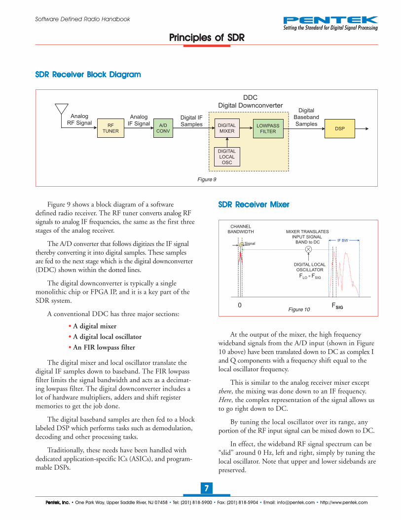
SDR RSDR RSDR RSDR RSDR Receiver Block Diagrameceiver Block Diagrameceiver Block Diagrameceiver Block Diagrameceiver Block Diagram
Figure 9
PPPPPrinciples of SDRrinciples of SDRrinciples of SDRrinciples of SDRrinciples of SDR
Figure 10
SDR RSDR RSDR RSDR RSDR Receiver Mixereceiver Mixereceiver Mixereceiver Mixereceiver MixerFigure 9 shows a block diagram of a softwaredefined radio receiver. The RF tuner converts analog RFsignals to analog IF frequencies, the same as the first threestages of the analog receiver.
The A/D converter that follows digitizes the IF signalthereby converting it into digital samples. These samplesare fed to the next stage which is the digital downconverter(DDC) shown within the dotted lines.
The digital downconverter is typically a singlemonolithic chip or FPGA IP, and it is a key part of theSDR system.
A conventional DDC has three major sections:
• A digital mixer
• A digital local oscillator
• An FIR lowpass filter
The digital mixer and local oscillator translate thedigital IF samples down to baseband. The FIR lowpassfilter limits the signal bandwidth and acts as a decimat-ing lowpass filter. The digital downconverter includes alot of hardware multipliers, adders and shift registermemories to get the job done.
The digital baseband samples are then fed to a blocklabeled DSP which performs tasks such as demodulation,decoding and other processing tasks.
Traditionally, these needs have been handled withdedicated application-specific ICs (ASICs), and program-mable DSPs.
At the output of the mixer, the high frequencywideband signals from the A/D input (shown in Figure10 above) have been translated down to DC as complex Iand Q components with a frequency shift equal to thelocal oscillator frequency.
This is similar to the analog receiver mixer exceptthere, the mixing was done down to an IF frequency.Here, the complex representation of the signal allows usto go right down to DC.
By tuning the local oscillator over its range, anyportion of the RF input signal can be mixed down to DC.
In effect, the wideband RF signal spectrum can be“slid” around 0 Hz, left and right, simply by tuning thelocal oscillator. Note that upper and lower sidebands arepreserved.

PPPPPentek, Inc.entek, Inc.entek, Inc.entek, Inc.entek, Inc. • One Park Way, Upper Saddle River, NJ 07458 • Tel: (201) 818-5900 • Fax: (201) 818-5904 • Email: [email protected] • http://www.pentek.com
88888
Software Defined Radio Handbook
DIGITAL
MIXER
DIGITAL
LOCAL
OSC
A/D
CONV
Digital IF
SamplesLOWPASS
FILTER
Digital
Baseband
Samples
Translation Filtering
Tuning Freq Decimation
DDC Signal PDDC Signal PDDC Signal PDDC Signal PDDC Signal Processingrocessingrocessingrocessingrocessing
Figure 12
PPPPPrinciples of SDRrinciples of SDRrinciples of SDRrinciples of SDRrinciples of SDR
Figure 11A Local Oscillator Frequency Switching
DDC LDDC LDDC LDDC LDDC Local Oscillator and Decimationocal Oscillator and Decimationocal Oscillator and Decimationocal Oscillator and Decimationocal Oscillator and Decimation
F1 F2 F3
90O
A/D Sample Rate(before decimation)
Sample Rate: Fs
Decimated
Filter OutputSample Rate: Fs/N
Figure 11B FIR Filter Decimation
Because the local oscillator uses a digital phaseaccumulator, it has some very nice features. It switchesbetween frequencies with phase continuity, so you cangenerate FSK signals or sweeps very precisely with notransients as shown in Figure 11A.
The frequency accuracy and stability are determinedentirely by the A/D clock so it’s inherently synchronousto the sampling frequency. There is no aging, drift orcalibration since it’s implemented entirely with digital logic.
Since the output of the FIR filter is band-limited, theNyquist theorem allows us to lower the sample rate. Ifwe are keeping only one out of every N samples, as shownin Figure 11B above, we have dropped the sampling rateby a factor of N.
This process is called decimation and it means keepingone out of every N signal samples. If the decimatedoutput sample rate is kept higher than twice the outputbandwidth, no information is lost.
The clear benefit is that decimated signals can beprocessed easier, can be transmitted at a lower rate, orstored in less memory. As a result, decimation candramatically reduce system costs!
As shown in Figure 12, the DDC performs twosignal processing operations:
1. Frequency translation with the tuning controlledby the local oscillator.
2. Lowpass filtering with the bandwidth controlledby the decimation setting.
We will next turn our attention to the Software-Defined Radio Transmitter.
PPPPPentek, Inc.entek, Inc.entek, Inc.entek, Inc.entek, Inc. • One Park Way, Upper Saddle River, NJ 07458 • Tel: (201) 818-5900 • Fax: (201) 818-5904 • Email: [email protected] • http://www.pentek.com
99999
Software Defined Radio Handbook
DUC Signal PDUC Signal PDUC Signal PDUC Signal PDUC Signal Processingrocessingrocessingrocessingrocessing
Figure 14
PPPPPrinciples of SDRrinciples of SDRrinciples of SDRrinciples of SDRrinciples of SDR
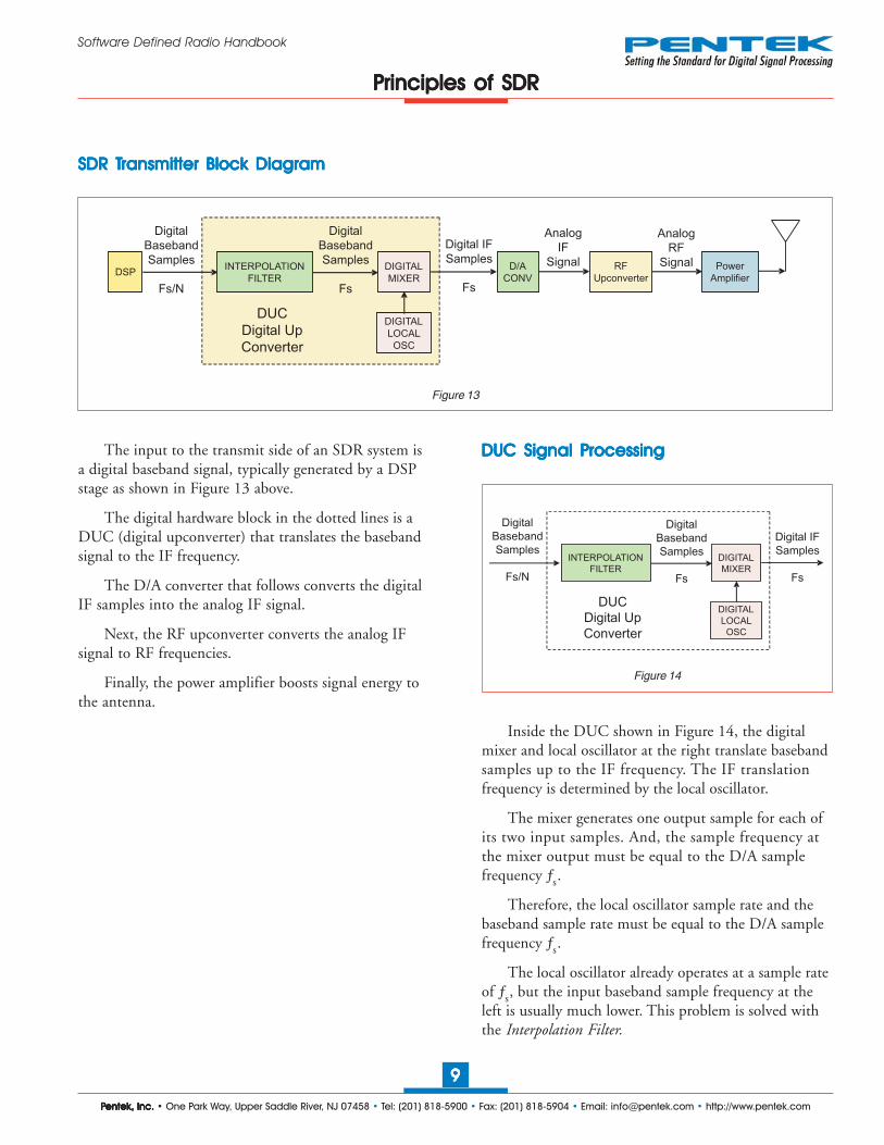
SDR TSDR TSDR TSDR TSDR Transmitter Block Diagramransmitter Block Diagramransmitter Block Diagramransmitter Block Diagramransmitter Block Diagram
Figure 13
The input to the transmit side of an SDR system isa digital baseband signal, typically generated by a DSPstage as shown in Figure 13 above.
The digital hardware block in the dotted lines is aDUC (digital upconverter) that translates the basebandsignal to the IF frequency.
The D/A converter that follows converts the digitalIF samples into the analog IF signal.
Next, the RF upconverter converts the analog IFsignal to RF frequencies.
Finally, the power amplifier boosts signal energy tothe antenna.
Inside the DUC shown in Figure 14, the digitalmixer and local oscillator at the right translate basebandsamples up to the IF frequency. The IF translationfrequency is determined by the local oscillator.
The mixer generates one output sample for each ofits two input samples. And, the sample frequency atthe mixer output must be equal to the D/A samplefrequency ƒs.
Therefore, the local oscillator sample rate and thebaseband sample rate must be equal to the D/A samplefrequency ƒs.
The local oscillator already operates at a sample rateof ƒs, but the input baseband sample frequency at theleft is usually much lower. This problem is solved withthe Interpolation Filter.
Digital
Baseband
Samples
Fs/N
DIGITAL
MIXER
DIGITAL
LOCAL
OSC
DUC
Digital Up
Converter
INTERPOLATION
FILTER
Digital IF
Samples
Fs
Digital
Baseband
Samples
Fs
DUC
Digital Up
Converter
Analog
IF
SignalD/A
CONV
Analog
RF
SignalRF
Upconverter
Power
AmplifierDSP
Digital
Baseband
Samples
Fs/N
DIGITAL
MIXER
DIGITAL
LOCAL
OSC
INTERPOLATION
FILTER
Digital IF
Samples
Fs
Digital
Baseband
Samples
Fs
PPPPPentek, Inc.entek, Inc.entek, Inc.entek, Inc.entek, Inc. • One Park Way, Upper Saddle River, NJ 07458 • Tel: (201) 818-5900 • Fax: (201) 818-5904 • Email: [email protected] • http://www.pentek.com
1010101010
Software Defined Radio Handbook
Interpolation FInterpolation FInterpolation FInterpolation FInterpolation Filter: Time domainilter: Time domainilter: Time domainilter: Time domainilter: Time domain
Figure 15 Figure 16
Interpolation FInterpolation FInterpolation FInterpolation FInterpolation Filter: Filter: Filter: Filter: Filter: Frequency Domainrequency Domainrequency Domainrequency Domainrequency Domain
PPPPPrinciples of SDRrinciples of SDRrinciples of SDRrinciples of SDRrinciples of SDR
INTERPOLATING
LOW PASS
FIR FILTER
Fs/N
I
Q
INTERPOLATION
FACTOR = N
BASEBAND
INPUT
Interpolating
Filter OutputSample Rate: Fs
Baseband InputSample Rate: Fs/N
Fs
INTER-
POLATED
OUTPUT
I
Q
0 IF Freq
LOCAL
OSCILLATOR
F = IF Freq
MIXER
INTERPOLATED
BASEBAND INPUT TRANSLATED OUTPUT
Digital
Baseband
Samples
Fs/N
DIGITAL
MIXER
DIGITAL
LOCAL
OSC
DUC
Digital Up
Converter
INTERPOLATION
FILTER
Digital IF
Samples
Fs
Digital
Baseband
Samples
Fs
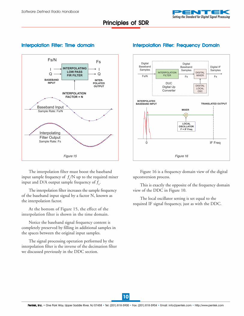
The interpolation filter must boost the basebandinput sample frequency of ƒs/N up to the required mixerinput and D/A output sample frequency of ƒs.
The interpolation filter increases the sample frequencyof the baseband input signal by a factor N, known asthe interpolation factor.
At the bottom of Figure 15, the effect of theinterpolation filter is shown in the time domain.
Notice the baseband signal frequency content iscompletely preserved by filling in additional samples inthe spaces between the original input samples.
The signal processing operation performed by theinterpolation filter is the inverse of the decimation filterwe discussed previously in the DDC section.
Figure 16 is a frequency domain view of the digitalupconversion process.
This is exactly the opposite of the frequency domainview of the DDC in Figure 10.
The local oscillator setting is set equal to therequired IF signal frequency, just as with the DDC.
PPPPPentek, Inc.entek, Inc.entek, Inc.entek, Inc.entek, Inc. • One Park Way, Upper Saddle River, NJ 07458 • Tel: (201) 818-5900 • Fax: (201) 818-5904 • Email: [email protected] • http://www.pentek.com
1111111111
Software Defined Radio Handbook
DIGITAL
MIXER
DIGITAL
LOCAL
OSC
¸ N
A/D
CONVLOWPASS
FILTER
Translation Filtering
DSP
Fs Fb
Tuning
Freq uency
Bandwidth
Deci mation
DIGITAL
MIXER
DIGITAL
LOCAL
OSC
´ N
INTERPOLATE
FILTER
TranslationFiltering
D/A
CONVDSP
Fb Fs
Tuning
Freq uencyInter polation
Bandwidth
DDC PDDC PDDC PDDC PDDC Processingrocessingrocessingrocessingrocessing DUC PDUC PDUC PDUC PDUC Processingrocessingrocessingrocessingrocessing
Figure 17 Figure 18
PPPPPrinciples of SDRrinciples of SDRrinciples of SDRrinciples of SDRrinciples of SDR
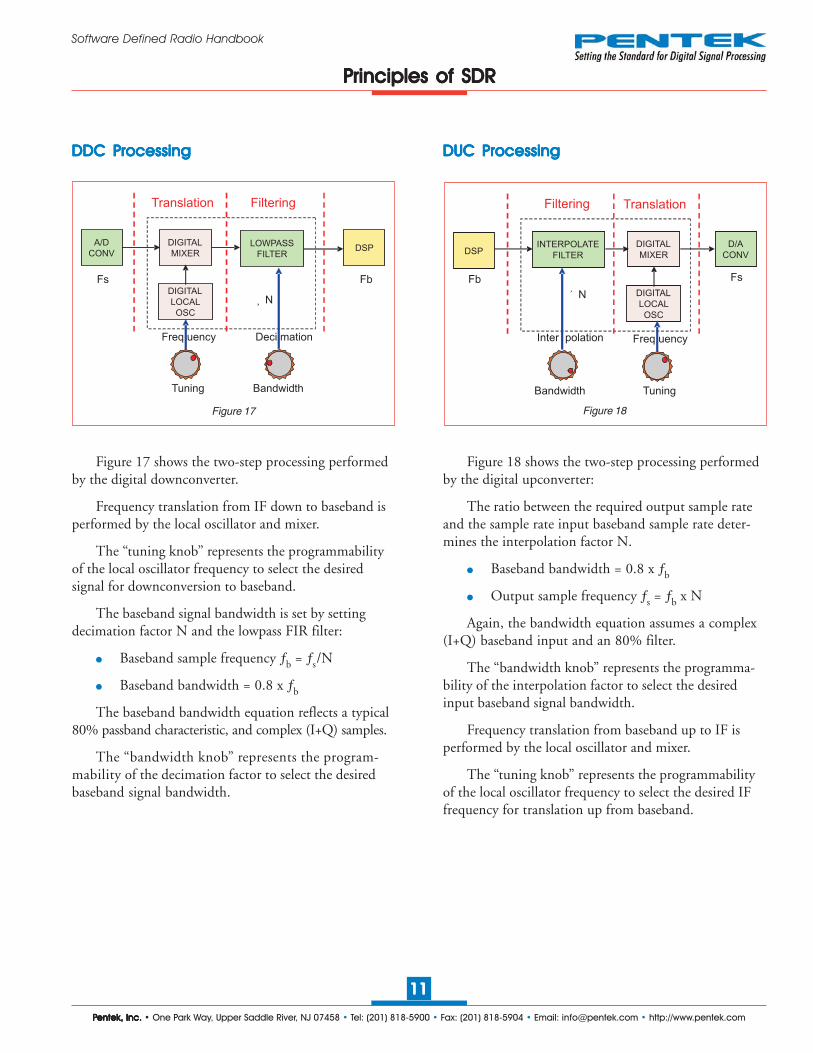
Figure 17 shows the two-step processing performedby the digital downconverter.
Frequency translation from IF down to baseband isperformed by the local oscillator and mixer.
The “tuning knob” represents the programmabilityof the local oscillator frequency to select the desiredsignal for downconversion to baseband.
The baseband signal bandwidth is set by settingdecimation factor N and the lowpass FIR filter:
● Baseband sample frequency ƒb = ƒs/N
● Baseband bandwidth = 0.8 x ƒb
The baseband bandwidth equation reflects a typical80% passband characteristic, and complex (I+Q) samples.
The “bandwidth knob” represents the program-mability of the decimation factor to select the desiredbaseband signal bandwidth.
Figure 18 shows the two-step processing performedby the digital upconverter:
The ratio between the required output sample rateand the sample rate input baseband sample rate deter-mines the interpolation factor N.
● Baseband bandwidth = 0.8 x ƒb
● Output sample frequency ƒs = ƒb x N
Again, the bandwidth equation assumes a complex(I+Q) baseband input and an 80% filter.
The “bandwidth knob” represents the programma-bility of the interpolation factor to select the desiredinput baseband signal bandwidth.
Frequency translation from baseband up to IF isperformed by the local oscillator and mixer.
The “tuning knob” represents the programmabilityof the local oscillator frequency to select the desired IFfrequency for translation up from baseband.
PPPPPentek, Inc.entek, Inc.entek, Inc.entek, Inc.entek, Inc. • One Park Way, Upper Saddle River, NJ 07458 • Tel: (201) 818-5900 • Fax: (201) 818-5904 • Email: [email protected] • http://www.pentek.com
1212121212
Software Defined Radio Handbook
KKKKKey DDC and DUCey DDC and DUCey DDC and DUCey DDC and DUCey DDC and DUC Benefits Benefits Benefits Benefits Benefits SDR TSDR TSDR TSDR TSDR Tasksasksasksasksasks
Figure 19
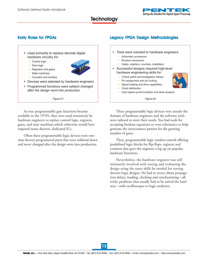
Here we’ve ranked some of the popular signalprocessing tasks associated with SDR systems on a twoaxis graph, with computational Processing Intensity onthe vertical axis and Flexibility on the horizontal axis.
What we mean by process intensity is the degree ofhighly-repetitive and rather primitive operations. At theupper left, are dedicated functions like A/D convertersand DDCs that require specialized hardware structuresto complete the operations in real time. ASICs are usuallychosen for these functions.
Flexibility pertains to the uniqueness or variabilityof the processing and how likely the function may haveto be changed or customized for any specific application.At the lower right are tasks like analysis and decisionmaking which are highly variable and often subjective.
Programmable general-purpose processors or DSPsare usually chosen for these tasks since these tasks can beeasily changed by software.
Now let’s temporarily step away from the softwareradio tasks and take a deeper look at programmablelogic devices.
Figure 20
DIGITAL
MIXER
DIGITAL
LOCAL
OSC
A/D
CONV
Digital IF
Samples
Fs
LOWPASS
FILTER
Digital
Baseband
Samples
Fs/N
DUC
Digital Up
Converter
D/A
CONV
Digital
Baseband
Samples
Fs/N
DIGITAL
MIXER
DIGITAL
LOCAL
OSC
INTERPOLATION
FILTER
Digital IF
Samples
Fs
Digital
Baseband
Samples
Fs
DUC
Digital Down
Converter
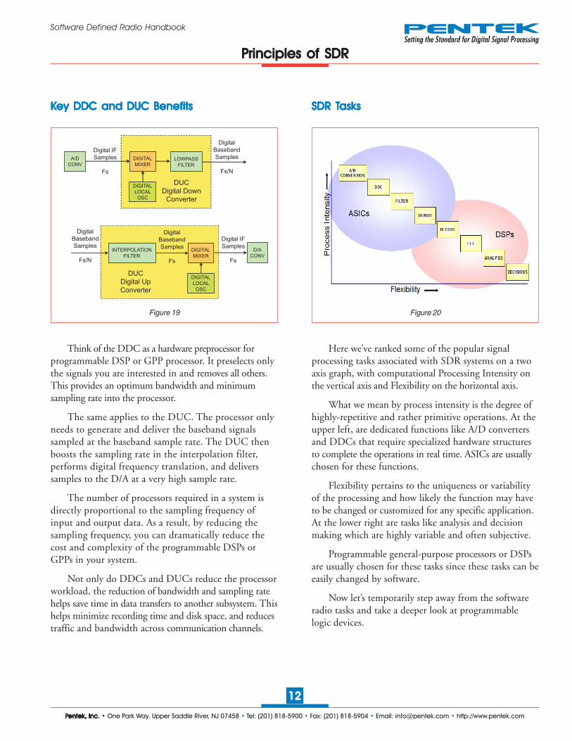
Think of the DDC as a hardware preprocessor forprogrammable DSP or GPP processor. It preselects onlythe signals you are interested in and removes all others.This provides an optimum bandwidth and minimumsampling rate into the processor.
The same applies to the DUC. The processor onlyneeds to generate and deliver the baseband signalssampled at the baseband sample rate. The DUC thenboosts the sampling rate in the interpolation filter,performs digital frequency translation, and deliverssamples to the D/A at a very high sample rate.
The number of processors required in a system isdirectly proportional to the sampling frequency ofinput and output data. As a result, by reducing thesampling frequency, you can dramatically reduce thecost and complexity of the programmable DSPs orGPPs in your system.
Not only do DDCs and DUCs reduce the processorworkload, the reduction of bandwidth and sampling ratehelps save time in data transfers to another subsystem. Thishelps minimize recording time and disk space, and reducestraffic and bandwidth across communication channels.
PPPPPrinciples of SDRrinciples of SDRrinciples of SDRrinciples of SDRrinciples of SDR
PPPPPentek, Inc.entek, Inc.entek, Inc.entek, Inc.entek, Inc. • One Park Way, Upper Saddle River, NJ 07458 • Tel: (201) 818-5900 • Fax: (201) 818-5904 • Email: [email protected] • http://www.pentek.com
1313131313
Software Defined Radio Handbook
Early REarly REarly REarly REarly Roles for FPGAsoles for FPGAsoles for FPGAsoles for FPGAsoles for FPGAs LLLLLegacy FPGA Design Methodologiesegacy FPGA Design Methodologiesegacy FPGA Design Methodologiesegacy FPGA Design Methodologiesegacy FPGA Design Methodologies
Figure 21 Figure 22
TTTTTechnologyechnologyechnologyechnologyechnology
As true programmable gate functions becameavailable in the 1970’s, they were used extensively byhardware engineers to replace control logic, registers,gates, and state machines which otherwise would haverequired many discrete, dedicated ICs.
Often these programmable logic devices were one-time factory-programmed parts that were soldered downand never changed after the design went into production.
These programmable logic devices were mostly thedomain of hardware engineers and the software toolswere tailored to meet their needs. You had tools foraccepting boolean equations or even schematics to helpgenerate the interconnect pattern for the growingnumber of gates.
Then, programmable logic vendors started offeringpredefined logic blocks for flip-flops, registers andcounters that gave the engineer a leg up on popularhardware functions.
Nevertheless, the hardware engineer was stillintimately involved with testing and evaluating thedesign using the same skills he needed for testingdiscrete logic designs. He had to worry about propaga-tion delays, loading, clocking and synchronizing—alltricky problems that usually had to be solved the hardway—with oscilloscopes or logic analyzers.
� Used primarily to replace discrete digital
hardware circuitry for:
� Control logic
� Glue logic
� Registers and gates
� State machines
� Counters and dividers
� Devices were selected by hardware engineers
� Programmed functions were seldom changed
after the design went into production
� Tools were oriented to hardware engineers
� Schematic processors
� Boolean processors
� Gates, registers, counters, multipliers
� Successful designs required high-level
hardware engineering skills for:
� Critical paths and propagation delays
� Pin assignment and pin locking
� Signal loading and drive capabilities
� Clock distribution
� Input signal synchronization and skew analysis
PPPPPentek, Inc.entek, Inc.entek, Inc.entek, Inc.entek, Inc. • One Park Way, Upper Saddle River, NJ 07458 • Tel: (201) 818-5900 • Fax: (201) 818-5904 • Email: [email protected] • http://www.pentek.com
1414141414
Software Defined Radio Handbook
FPGAs: New Device TFPGAs: New Device TFPGAs: New Device TFPGAs: New Device TFPGAs: New Device Technologyechnologyechnologyechnologyechnology FPGAs: New Development TFPGAs: New Development TFPGAs: New Development TFPGAs: New Development TFPGAs: New Development Toolsoolsoolsoolsools
Figure 23 Figure 24
TTTTTechnologyechnologyechnologyechnologyechnology
It’s virtually impossible to keep up to date on FPGAtechnology, since new advancements are being madeevery day.
The hottest features are processor cores inside thechip, computation clocks to 500 MHz and above, andlower core voltages to keep power and heat down.
Several years ago, dedicated hardware multipliersstarted appearing and now you’ll find literally thousandsof them on-chip as part of the DSP initiative launchedby virtually all FPGA vendors.
High memory densities coupled with very flexiblememory structures meet a wide range of data flowstrategies. Logic slices with the equivalent of over tenmillion gates result from silicon geometries shrinkingbelow 0.1 micron.
BGA and flip-chip packages provide plenty of I/Opins to support on-board gigabit serial transceivers andother user-configurable system interfaces.
New announcements seem to be coming out everyday from chip vendors like Xilinx and Altera in a never-ending game of outperforming the competition.
To support such powerful devices, new design toolsare appearing that now open up FPGAs to both hard-ware and software engineers. Instead of just acceptinglogic equations and schematics, these new tools acceptentire block diagrams as well as VHDL and Verilogdefinitions.
Choosing the best FPGA vendor often hingesheavily on the quality of the design tools available tosupport the parts.
Excellent simulation and modeling tools help toquickly analyze worst case propagation delays andsuggest alternate routing strategies to minimize themwithin the part. This minimizes some of the trickytiming work for hardware engineers and can save onehours of tedious troubleshooting during design verifica-tion and production testing.
In the last few years, a new industry of third partyIP (Intellectual Property) core vendors now offerthousands of application-specific algorithms. These areready to drop into the FPGA design process to help beatthe time-to-market crunch and to minimize risk.
� High Level Design Tools
� Block Diagram System Generators
� Schematic Processors
� High-level language compilers for
VHDL & Verilog
� Advanced simulation tools for modeling speed,
propagation delays, skew and board layout
� Faster compilers and simulators save time
� Graphically-oriented debugging tools
� IP (Intellectual Property) Cores
� FPGA vendors offer both free and licensed cores
� FPGA vendors promote third party core vendors
� Wide range of IP cores available
� 500+ MHz DSP Slices and Memory Structures
Over 3500 dedicated on-chip hardware multipliers
On-board GHz Serial Transceivers
Partial Reconfigurability Maintains
Operation During Changes
Switched Fabric Interface Engines
Over 690,000 Logic Cells
Gigabit Ethernet media access controllers
On-chip 405 PowerPC RISC micro-controller cores
Memory densities approaching 85 million bits
Reduced power with core voltages at 1 volt
Silicon geometries to 28 nanometers
High-density BGA and flip-chip packaging
Over 1200 user I/O pins
Configurable logic and I/O interface standards
�
�
�
�
�
�
�
�
�
�
�
�
�
�
PPPPPentek, Inc.entek, Inc.entek, Inc.entek, Inc.entek, Inc. • One Park Way, Upper Saddle River, NJ 07458 • Tel: (201) 818-5900 • Fax: (201) 818-5904 • Email: [email protected] • http://www.pentek.com
1515151515
Software Defined Radio Handbook
FPGAs for SDRFPGAs for SDRFPGAs for SDRFPGAs for SDRFPGAs for SDR FPGAs Bridge the SDR Application SpaceFPGAs Bridge the SDR Application SpaceFPGAs Bridge the SDR Application SpaceFPGAs Bridge the SDR Application SpaceFPGAs Bridge the SDR Application Space
Figure 25 Figure 26
TTTTTechnologyechnologyechnologyechnologyechnology
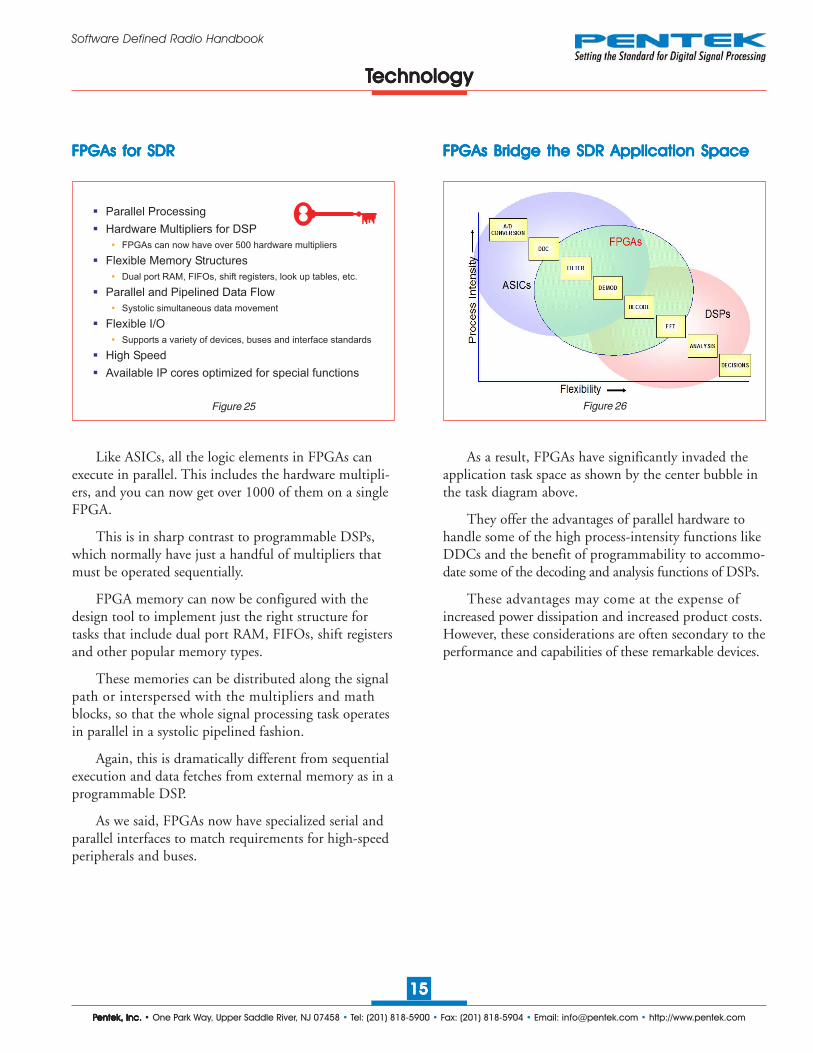
As a result, FPGAs have significantly invaded theapplication task space as shown by the center bubble inthe task diagram above.
They offer the advantages of parallel hardware tohandle some of the high process-intensity functions likeDDCs and the benefit of programmability to accommo-date some of the decoding and analysis functions of DSPs.
These advantages may come at the expense ofincreased power dissipation and increased product costs.However, these considerations are often secondary to theperformance and capabilities of these remarkable devices.
Like ASICs, all the logic elements in FPGAs canexecute in parallel. This includes the hardware multipli-ers, and you can now get over 1000 of them on a singleFPGA.
This is in sharp contrast to programmable DSPs,which normally have just a handful of multipliers thatmust be operated sequentially.
FPGA memory can now be configured with thedesign tool to implement just the right structure fortasks that include dual port RAM, FIFOs, shift registersand other popular memory types.
These memories can be distributed along the signalpath or interspersed with the multipliers and mathblocks, so that the whole signal processing task operatesin parallel in a systolic pipelined fashion.
Again, this is dramatically different from sequentialexecution and data fetches from external memory as in aprogrammable DSP.
As we said, FPGAs now have specialized serial andparallel interfaces to match requirements for high-speedperipherals and buses.
� Parallel Processing
� Hardware Multipliers for DSP
� FPGAs can now have over 500 hardware multipliers
� Flexible Memory Structures
� Dual port RAM, FIFOs, shift registers, look up tables, etc.
� Parallel and Pipelined Data Flow
� Systolic simultaneous data movement
� Flexible I/O
� Supports a variety of devices, buses and interface standards
� High Speed
� Available IP cores optimized for special functions

PPPPPentek, Inc.entek, Inc.entek, Inc.entek, Inc.entek, Inc. • One Park Way, Upper Saddle River, NJ 07458 • Tel: (201) 818-5900 • Fax: (201) 818-5904 • Email: [email protected] • http://www.pentek.com
1616161616
Software Defined Radio Handbook
The above chart shows the salient characteristics forsome of Pentek’s SDR products with factory-instlled IPcores. All these products are available off-the-self and arein the Pentek datasheets and catalogs.
The chart provides information regarding the numberof input channels, maximum sampling frequency of theirA/Ds, the number of bits, and number of DDC chan-nels in each one. This information is followed by DDCcharacteristics such as number of DDC channels and thedecimation range.
TTTTTechnologyechnologyechnologyechnologyechnology
TTTTTypical Pypical Pypical Pypical Pypical Pentek Pentek Pentek Pentek Pentek Products with Froducts with Froducts with Froducts with Froducts with Factoractoractoractoractoryyyyy-Installed SDR IP Cores-Installed SDR IP Cores-Installed SDR IP Cores-Installed SDR IP Cores-Installed SDR IP Cores
Other information that’s specific to each core isincluded as well as an indication of the models thatinclude an interpolation filter and output D/A. As shownin the chart, many of these models include features thatare critical for beamforming and direction-findingapplications.
All the models shown here are PMC or XMC modules.As with all Pentek SDR products, these models are alsoavailable in CompactPCI, PCI Express, OpenVPX, andAMC formats as well.
Figure 27
AnalogAnalogAnalogAnalogAnalog SamplingSamplingSamplingSamplingSampling InputInputInputInputInput DDCDDCDDCDDCDDC DecimationDecimationDecimationDecimationDecimation OutputOutputOutputOutputOutput DUCDUCDUCDUCDUC Interpol.Interpol.Interpol.Interpol.Interpol. Beam-Beam-Beam-Beam-Beam-
ModelModelModelModelModel ChannelsChannelsChannelsChannelsChannels FFFFFreq (max)req (max)req (max)req (max)req (max) BitsBitsBitsBitsBits ChannelsChannelsChannelsChannelsChannels RRRRRangeangeangeangeange BitsBitsBitsBitsBits ChannelsChannelsChannelsChannelsChannels RRRRRangeangeangeangeange formerformerformerformerformer
7142-428 4 125 MHz 14 4 2–64K 16 or 24 None None No
7151 4 200 MHz 16 256 128–1K 16 or 24 None None No
7152 4 200 MHz 16 32 16–8K 16 or 24 None None Yes
7153 4 200 MHz 16 2 or 4 2–64K/2–256 16 or 24 None None Yes
71621 3 200 MHz 16 3 2–64K 16 or 24 1 2–512K Yes
71641 1 or 2 3.6 or 1.8 GHz 12 1 or 2 4, 8 or 16 16 None None No
71651 2 500/400 MHz 12/14 2 2–128K 16 or 24 1 2–512K Yes
71661 4 200 MHz 16 4 2–64K 16 or 24 None None Yes
71662 4 200 MHz 16 32 16–8K 24 None None No
71671 None None – None – 16 4 2–1024K No

PPPPPentek, Inc.entek, Inc.entek, Inc.entek, Inc.entek, Inc. • One Park Way, Upper Saddle River, NJ 07458 • Tel: (201) 818-5900 • Fax: (201) 818-5904 • Email: [email protected] • http://www.pentek.com
1717171717
Software Defined Radio Handbook
TTTTTechnologyechnologyechnologyechnologyechnology
FPGA RFPGA RFPGA RFPGA RFPGA Resource Comparisonesource Comparisonesource Comparisonesource Comparisonesource Comparison
Figure 28
The above chart compares the available resources inthe five Xilinx FPGA families that are used in most ofthe Pentek products.
● Virtex-II Pro: VP● Virtex-4: FX, LX and SX● Virtex-5: LX and SX● Virtex-6: LX and SX● Virtex-7: VX
The Virtex-II family includes hardware multipliersthat support digital filters, averagers, demodulatorsand FFTs—a major benefit for software radio signalprocessing. The Virtex-II Pro family dramaticallyincreased the number of hardware multipliers and alsoadded embedded PowerPC microcontrollers.
The Virtex-4 family is offered as three subfamiliesthat dramatically boost clock speeds and reduce powerdissipation over previous generations.
The Virtex-4 LX family delivers maximum logic andI/O pins while the SX family boasts of 512 DSP slicesfor maximum DSP performance. The FX family is agenerous mix of all resources and is the only family tooffer RocketIO, PowerPC cores, and the newly addedgigabit Ethenet ports.
*Virtex-II Pro and Virtex-4 Slices actually require 2.25 Logic Cells;*Virtex-5, Virtex-6 and Virtex-7 Slices actually require 6.4 Logic Cells
VirVirVirVirVirtex-II Ptex-II Ptex-II Ptex-II Ptex-II Prororororo VirVirVirVirVirtex-4tex-4tex-4tex-4tex-4 VirVirVirVirVirtex-5tex-5tex-5tex-5tex-5 VirVirVirVirVirtex-6tex-6tex-6tex-6tex-6 VirVirVirVirVirtex-7tex-7tex-7tex-7tex-7VPVPVPVPVP FX, LX, SXFX, LX, SXFX, LX, SXFX, LX, SXFX, LX, SX LX, SXLX, SXLX, SXLX, SXLX, SX LX, SXLX, SXLX, SXLX, SXLX, SX VXVXVXVXVX
Logic Cells 53K–74K 55K–110K 52K–155K 128K–314K 326K–693KSlices* 23K–33K 24K–49K 8K–24K 20K–49K 51K–108KCLB Flip-Flops 46K–66K 48K–98K 32K–96K 160K–392K 408K–864KBlock RAM (kb) 4,176–5,904 4,176–6,768 4,752–8,784 9,504–25,344 27,000–52,920DSP Hard IP 18x18 Multipliers DSP48 DSP48E DSP48E DSP48EDSP Slices 232–328 96–512 128–640 480–1,344 1,120–3,600Serial Gbit Transceivers N/A 0–20 12–16 20–24 28–80PCI Express Support N/A N/A N/A Gen 2 x8 Gen 2 x8, Gen 3 x8User I/O 852–996 576–960 480–680 600–720 700–1,000
The Virtex-5 family LX devices offer maximumlogic resources, gigabit serial transceivers, and Ethernetmedia access controllers. The SX devices push DSPcapabilities with all of the same extras as the LX.
The Virtex-5 devices offer lower power dissipation,faster clock speeds and enhanced logic slices. They alsoimprove the clocking features to handle faster memoryand gigabit interfaces. They support faster single-endedand differential parallel I/O buses to handle fasterperipheral devices.
The Virtex-6 and Virtex-7 devices offer still higherdensity, more processing power, lower power consump-tion, and updated interface features to match the latesttechnology I/O requirements including PCI Express.Virtex-6 supports PCIe 2.0 and Virtex-7 supports PCIe 3.0
The ample DSP slices are responsible for themajority of the processing power of the Virtex-6 andVirtex-7 families. Increases in operating speed from 500 MHzin V-4, to 550 MHz in V-5, to 600 MHz in V-6, to900 MHz in V-7 and continuously increasing densityallow more DSP slices to be included in the same-sizepackage. As shown in the chart, Virtex-6 tops out at animpressive 1,344 DSP slices, while Virtex-7 tops out atan even more impressive 3,600 DSP slices.

PPPPPentek, Inc.entek, Inc.entek, Inc.entek, Inc.entek, Inc. • One Park Way, Upper Saddle River, NJ 07458 • Tel: (201) 818-5900 • Fax: (201) 818-5904 • Email: [email protected] • http://www.pentek.com
1818181818
Software Defined Radio Handbook
The Pentek family of board-level software radioproducts is the most comprehensive in the industry.Most of these products are available in several formatsto satisfy a wide range of requirements.
In addition to their commercial versions, manysoftware radio products are available in ruggedized andconduction-cooled versions.
Most of the software radio products include input A/Dconverters. Some of these products are software radioreceivers in that they include only DDCs. Others aresoftware radio transceivers and they include DDCs aswell as DUCs with output D/A converters. These comewith independent input and output clocks.
All Pentek software radio products include multiboardsynchronization that facilitates the design of multichannelsystems with synchronous clocking, gating and triggering.
Pentek’s comprehensive software support includesthe ReadyFlow® Board Support Package, the GateFlow®
FPGA Design Kit and high-performance factory-installed IP cores that expand the features and rangeof many Pentek software radio products. In addition,Pentek high-speed recording systems are supported withSystemFlow® recording software that features a graphicaluser interface.
In addition to product overviews presented in thepages that follow, a complete listing of these productswith active links to their datasheets on Pentek’s website isincluded at the end of this handbook.
PPPPProductsroductsroductsroductsroducts
Figure 29
PMC, XMC, CompactPCI, PCI, PCI Express, OpenVPX, AMC, and VMEbus SofPMC, XMC, CompactPCI, PCI, PCI Express, OpenVPX, AMC, and VMEbus SofPMC, XMC, CompactPCI, PCI, PCI Express, OpenVPX, AMC, and VMEbus SofPMC, XMC, CompactPCI, PCI, PCI Express, OpenVPX, AMC, and VMEbus SofPMC, XMC, CompactPCI, PCI, PCI Express, OpenVPX, AMC, and VMEbus Software Rtware Rtware Rtware Rtware Radioadioadioadioadio
PMC/XMC Module
6U CompactPCIBoard
PCI Board
Full-lengthPCI Express Board
Half-lengthPCI Express Board
VMEbus Board
3U OpenVPX BoardsCOTS and Rugged
AMC Board

PPPPPentek, Inc.entek, Inc.entek, Inc.entek, Inc.entek, Inc. • One Park Way, Upper Saddle River, NJ 07458 • Tel: (201) 818-5900 • Fax: (201) 818-5904 • Email: [email protected] • http://www.pentek.com
1919191919
Software Defined Radio Handbook
DDR 2
SDRAM
256 MB
DDR 2
SDRAM
256 MB
DDR 2
SDRAM
256 MB
32 32 32
32
RF
XFORMR
RF Out
DAC5686
DIGITAL
UPCONVERTER
16-bit D/A
RF
XFORMR
LTC2255
125MHz
14-bit A/D
RF In
14
RF
XFORMR
LTC2255
125MHz
14-bit A/D
RF In
14
RF
XFORMR
LTC2255
125MHz
14-bit A/D
RF In
14
RF
XFORMR
LTC2255
125MHz
14-bit A/D
RF In
14
P15 XMC
VITA 42.0
P4 PMC
FPGA I/O
(Option –104)
64
64LOCAL
BUS
VIRTEX-4 FPGA
XC4VFX60 or XC4VFX100
PCI BUS
(64 Bits / 66 MHz)
PCI 2.2
INTERFACE
SERIAL
INTERFACE
32 32 32HI-SPEED
BUSES
VIRTEX-4 FPGA
XC4VSX55
DSP – Channelizer – Digital Delay – Demodulation – Decoding – Control – etc.
Control/
Status
TIMING BUS
GENERATOR A
XTL
OSC A
SYNC
INTERRUPTS
& CONTROL
TIMING BUS
GENERATOR B
XTL
OSC B
LVDS Clock A
LVDS Sync A
LVDS Gate A
TTL Gate/
Trigger
TTL Sync
LVDS Clock B
LVDS Sync B
LVDS Gate B
Clock/Sync/Gate
Bus A
Clock/Sync/Gate
Bus B
To All
Sections
Sample
Clock In
Multichannel TMultichannel TMultichannel TMultichannel TMultichannel Transceivers with Virransceivers with Virransceivers with Virransceivers with Virransceivers with Virtex-4 FPGAstex-4 FPGAstex-4 FPGAstex-4 FPGAstex-4 FPGAs
PPPPProductsroductsroductsroductsroducts
Model 7142PMC/XMC
Figure 30
The Model 7142 is a Multichannel PMC/XMCmodule. It includes four 125 MHz 14-bit A/D convert-ers and one upconverter with a 500 MHz 16-bit D/Aconverter to support wideband receive and transmitcommunication channels.
Two Xilinx Virtex-4 FPGAs are included: anXC4VSX55 or LX100 and an XC4VFX60 or FX100.The first FPGA is used for control and signal processingfunctions, while the second one is used for implement-ing board interface functions including the XMC interface.
It also features 768 MB of SDRAM for implementingup to 2.0 sec of transient capture or digital delay memoryfor signal intelligence tracking applications at 125 MHz.
A 16 MB flash memory supports the boot code forthe two on-board IBM 405 PowerPC microcontrollercores within the FPGA.
A 9-channel DMA controller and 64 bit / 66 MHz PCIinterface assures efficient transfers to and from the module.
A high-performance 160 MHz IP core wideband digitaldownconverter may be factory-installed in the first FPGA.
Two 4X switched serial ports, implemented with theXilinx Rocket I/O interfaces, connect the second FPGAto the XMC connector with two 2.5 GB/sec data linksto the carrier board.
A dual bus system timing generator allows separateclocks, gates and synchronization signals for the A/Dand D/A converters. It also supports large, multichannelapplications where the relative phases must be preserved.
Versions of the 7142 are also available as a PCIe full-length board (Models 7742 and 7742D dual density),PCIe half-length board (Model 7842), 3U VPX (Model5342), PCI board (Model 7642), 6U cPCI (Models 7242and 7242D dual density), and 3U cPCI (Model 7342).
Model 714Model 714Model 714Model 714Model 71422222 PMC/XMC PMC/XMC PMC/XMC PMC/XMC PMC/XMC ●●●●● Model 724 Model 724 Model 724 Model 724 Model 72422222 6U cPCI 6U cPCI 6U cPCI 6U cPCI 6U cPCI ●●●●● Model 734 Model 734 Model 734 Model 734 Model 73422222 3U cPCI 3U cPCI 3U cPCI 3U cPCI 3U cPCI ●●●●● Model 764Model 764Model 764Model 764Model 76422222 PCI PCI PCI PCI PCIModel 7Model 7Model 7Model 7Model 777777444442 F2 F2 F2 F2 Full-lengthull-lengthull-lengthull-lengthull-length PCIe PCIe PCIe PCIe PCIe ●●●●● Model 7 Model 7 Model 7 Model 7 Model 788888444442 Half-length2 Half-length2 Half-length2 Half-length2 Half-length PCIe PCIe PCIe PCIe PCIe ●●●●● Model Model Model Model Model 55555343434343422222 3U 3U 3U 3U 3U VPXVPXVPXVPXVPX
PPPPPentek, Inc.entek, Inc.entek, Inc.entek, Inc.entek, Inc. • One Park Way, Upper Saddle River, NJ 07458 • Tel: (201) 818-5900 • Fax: (201) 818-5904 • Email: [email protected] • http://www.pentek.com
2020202020
Software Defined Radio Handbook
TTTTTransceivers with Fransceivers with Fransceivers with Fransceivers with Fransceivers with Four Multiband DDCs and Interpolation Four Multiband DDCs and Interpolation Four Multiband DDCs and Interpolation Four Multiband DDCs and Interpolation Four Multiband DDCs and Interpolation Filter Installed Coresilter Installed Coresilter Installed Coresilter Installed Coresilter Installed Cores
PPPPProductsroductsroductsroductsroducts
Figure 31
.
RF
XFORMR
RF
XFORMR
RF
XFORMR
AD6645
105 MHz
14-bit A/D
CLOCK &
SYNC
GENERATOR
DAC 5686
DIGITAL
UPCONVERTER
16-bit
500 MHZ
D/A
PCI 2.2
INTERFACE
MEMORY
CONTROL &
DATA ROUTING
D/A
FIFO
MUXCFIR
FILTER
CIC
FILTER
MUX
DIGITAL
DOWNCONVERTR A
STAGE 1
DECIMATION: 2 – 256
CH A
RF In
CH B
RF In
RF Out
Sample
Clock In
Clock/Sync
Bus
A/D A
A/D A
A/D B
A/D A
MEMORY
D/A FIFO
PCI BUS
64 bit /
66 MHz
DIGITAL DOWNCONVERTER CORE
INTERPOLATION CORE XC4VSX55
RF
XFORMR
RF
XFORMR
RF
XFORMR
LTC2255
125 MHz
14-bit A/D
CLOCK &
SYNC
GENERATOR
XTAL
OSC A
XTAL
OSC B
DAC 5686
DIGITAL
UPCONVERTER
16-bit
500 MHZ
D/A
PCI 2.2
INTERFACE
LTC2255
125 MHz
14-bit A/D
RF
XFORMR
CH C
RF In
RF
XFORMR
LTC2255
125 MHz
14-bit A/D
RF
XFORMR
CH D
RF In
RF
XFORMR
LTC2255
125 MHz
14-bit A/D
A/D B
A/D C
A/D D
A/D C
A/D D
DIGITAL
DOWNCONVERTR A
STAGE 2
DECIMATION: 1 – 256
DIGITAL
DOWNCONVERTR B
STAGE 1
DECIMATION: 2 – 256
A/D A
A/D B
A/D C
A/D D
DIGITAL
DOWNCONVERTR B
STAGE 2
DECIMATION: 1 – 256
DIGITAL
DOWNCONVERTR C
STAGE 1
DECIMATION: 2 – 256
A/D A
A/D B
A/D C
A/D D
DIGITAL
DOWNCONVERTR C
STAGE 2
DECIMATION: 1 – 256
DIGITAL
DOWNCONVERTR D
STAGE 1
DECIMATION: 2 – 256
A/D A
A/D B
A/D C
A/D D
DIGITAL
DOWNCONVERTR D
STAGE 2
DECIMATION: 1 – 256
DDC A
MUX
A/D B
DDC B
MUX
A/D C
DDC C
MUX
A/D D
DDC D
D/A
M
U
X
M
U
X
M
U
X
M
U
X
MEM W
FIFO
MEM W
FIFO
A/D A
FIFO
A/D B
FIFO
A/D C
FIFO
A/D D
FIFO
256 MB DDR
SDRAM
256 MB DDR
SDRAM
256 MB DDR
SDRAM
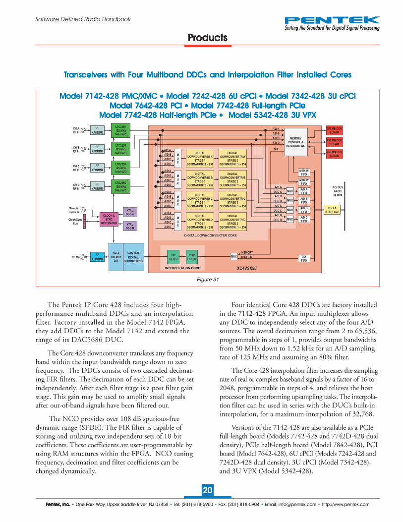
The Pentek IP Core 428 includes four high-performance multiband DDCs and an interpolationfilter. Factory-installed in the Model 7142 FPGA,they add DDCs to the Model 7142 and extend therange of its DAC5686 DUC.
The Core 428 downconverter translates any frequencyband within the input bandwidth range down to zerofrequency. The DDCs consist of two cascaded decimat-ing FIR filters. The decimation of each DDC can be setindependently. After each filter stage is a post filter gainstage. This gain may be used to amplify small signalsafter out-of-band signals have been filtered out.
The NCO provides over 108 dB spurious-freedynamic range (SFDR). The FIR filter is capable ofstoring and utilizing two independent sets of 18-bitcoefficients. These coefficients are user-programmable byusing RAM structures within the FPGA. NCO tuningfrequency, decimation and filter coefficients can bechanged dynamically.
Four identical Core 428 DDCs are factory installedin the 7142-428 FPGA. An input multiplexer allowsany DDC to independently select any of the four A/Dsources. The overal decimation range from 2 to 65,536,programmable in steps of 1, provides output bandwidthsfrom 50 MHz down to 1.52 kHz for an A/D samplingrate of 125 MHz and assuming an 80% filter.
The Core 428 interpolation filter increases the samplingrate of real or complex baseband signals by a factor of 16 to2048, programmable in steps of 4, and relieves the hostprocessor from performing upsampling tasks. The interpola-tion filter can be used in series with the DUC’s built-ininterpolation, for a maximum interpolation of 32,768.
Versions of the 7142-428 are also available as a PCIefull-length board (Models 7742-428 and 7742D-428 dualdensity), PCIe half-length board (Model 7842-428), PCIboard (Model 7642-428), 6U cPCI (Models 7242-428 and7242D-428 dual density), 3U cPCI (Model 7342-428),and 3U VPX (Model 5342-428).
Model 714Model 714Model 714Model 714Model 7142-4282-4282-4282-4282-428 PMC/XMC PMC/XMC PMC/XMC PMC/XMC PMC/XMC ●●●●● Model 724 Model 724 Model 724 Model 724 Model 7242-4282-4282-4282-4282-428 6U cPCI 6U cPCI 6U cPCI 6U cPCI 6U cPCI ●●●●● Model 734 Model 734 Model 734 Model 734 Model 7342-4282-4282-4282-4282-428 3U cPCI 3U cPCI 3U cPCI 3U cPCI 3U cPCIModel 7642-428 PCI Model 7642-428 PCI Model 7642-428 PCI Model 7642-428 PCI Model 7642-428 PCI ●●●●● Model 7742-428 F Model 7742-428 F Model 7742-428 F Model 7742-428 F Model 7742-428 Full-length PCIeull-length PCIeull-length PCIeull-length PCIeull-length PCIe
Model 7742-428 Model 7742-428 Model 7742-428 Model 7742-428 Model 7742-428 HalfHalfHalfHalfHalf-length PCIe-length PCIe-length PCIe-length PCIe-length PCIe ●●●●● Model Model Model Model Model 5555534343434342-4282-4282-4282-4282-428 3U 3U 3U 3U 3U VPXVPXVPXVPXVPX

PPPPPentek, Inc.entek, Inc.entek, Inc.entek, Inc.entek, Inc. • One Park Way, Upper Saddle River, NJ 07458 • Tel: (201) 818-5900 • Fax: (201) 818-5904 • Email: [email protected] • http://www.pentek.com
2121212121
Software Defined Radio Handbook
PPPPProductsroductsroductsroductsroducts
Model 7150 is a quad, high-speed data convertersuitable for connection as the HF or IF input of acommunications system. It features four 200 MHz,16-bit A/Ds supported by an array of data processingand transport resources idealy matched to the require-ments of high-performance systems. Model 7150 usesthe popular PMC format and supports the emergingVITA 42 XMC standard for switched fabric interfaces.
The Model 7150 architecture includes two Virtex-5FPGAs. The first FPGA is used primarily for signalprocessing while the second one is dedicated to boardinterfaces. All of the board’s data and control paths areaccessible by the FPGAs, enabling factory installedfunctions including data multiplexing, channel selection, datapacking, gating, triggering and SDRAM memory control.
Three independent 512 MB banks of DDR2SDRAM are available to the signal processing FPGA.Built-in memory functions include an A/D data transient
RF In
16
ADS5485
200 MHz
16-bit A/D
RF In
16
ADS5485
200 MHz
16-bit A/D
RF In
16
ADS5485
200 MHz
16-bit A/D
RF
XFORMR
RF In
16
ADS5485
200 MHz
16-bit A/D
RF
XFORMR
RF
XFORMR
RF
XFORMR
TIMING BUS
GENERATOR
Clock/ Sync /
Gate / PPS
XTL
OSC
Sample Clock In
TTL Gate / Trigger
Clock/Sync/
Gate/PPS Bus
TTL Sync / PPS
Sample Clk
Sync Clk
Gate A
Gate B
Sync
PPS
PPS In
PROCESSING FPGA
VIRTEX –5: LX50T, SX50T, SX95T, LX155T or FX100TTo All
Sections
Control/
Status
LOCAL BUS GTP GTP GTP
INTERFACE FPGA
VIRTEX-5: LX30T, SX50T or FX70T
PCI-X BUS
(32 or 64 Bits / 33, 66, 100 or 133 MHz)
P15 XMC
VITA 42.0
(Serial RapidIO,
PCI-Express,
etc.)P4 PMC
FPGA I/O
64
64
LOCAL BUS
x4
x4
x4x4
GTP
PCI-X LVDS GTP
x8
DDR 2
SDRAM
512 MB
1632 32 32
DDR 2
SDRAM
512 MB
DDR 2
SDRAM
512 MB
FLASH
32 MB
Model 7150PMC/XMC
capture mode with pre- and post-triggering. All memorybanks can be easily accessed through the PCI-X interface.
A 9-channel DMA controller and 64 bit / 100 MHzPCI-X interface assures efficient transfers to and from themodule.
Two 4X switched serial ports, implemented with theXilinx Rocket I/O interfaces, connect the FPGA to theXMC connector with two 2.5 GB/sec data links to thecarrier board.
A dual bus system timing generator allows separateclocks, gates and synchronization signals for the A/Dconverters. It also supports large, multichannel applica-tions where the relative phases must be preserved.
Versions of the 7150 are also available as a PCIe full-length board (Models 7750 and 7750D dual density),PCIe half-length board (Model 7850), PCI board (Model7650), 6U cPCI (Models 7250 and 7250D dual density),3U cPCI (Model 7350), and 3U VPX (Model 5350).
Quad 200 MHz 16-bit A/D with VirQuad 200 MHz 16-bit A/D with VirQuad 200 MHz 16-bit A/D with VirQuad 200 MHz 16-bit A/D with VirQuad 200 MHz 16-bit A/D with Virtex-5 FPGAstex-5 FPGAstex-5 FPGAstex-5 FPGAstex-5 FPGAs
Model 7150 PMC/XMC Model 7150 PMC/XMC Model 7150 PMC/XMC Model 7150 PMC/XMC Model 7150 PMC/XMC ●●●●● Model 7250 6U cPCI Model 7250 6U cPCI Model 7250 6U cPCI Model 7250 6U cPCI Model 7250 6U cPCI ●●●●● Model 7350 3U cPCI Model 7350 3U cPCI Model 7350 3U cPCI Model 7350 3U cPCI Model 7350 3U cPCI ●●●●● Model 7650 PCI Model 7650 PCI Model 7650 PCI Model 7650 PCI Model 7650 PCIModel 7750 FModel 7750 FModel 7750 FModel 7750 FModel 7750 Full-length PCIe ull-length PCIe ull-length PCIe ull-length PCIe ull-length PCIe ●●●●● Model 7850 Half-length PCIe Model 7850 Half-length PCIe Model 7850 Half-length PCIe Model 7850 Half-length PCIe Model 7850 Half-length PCIe ●●●●● Model 5350 3U VPX Model 5350 3U VPX Model 5350 3U VPX Model 5350 3U VPX Model 5350 3U VPX
Figure 32

PPPPPentek, Inc.entek, Inc.entek, Inc.entek, Inc.entek, Inc. • One Park Way, Upper Saddle River, NJ 07458 • Tel: (201) 818-5900 • Fax: (201) 818-5904 • Email: [email protected] • http://www.pentek.com
2222222222
Software Defined Radio Handbook
256- 256- 256- 256- 256-Channel DDC Installed Core with Quad 200 MHz, 16-bit A/DChannel DDC Installed Core with Quad 200 MHz, 16-bit A/DChannel DDC Installed Core with Quad 200 MHz, 16-bit A/DChannel DDC Installed Core with Quad 200 MHz, 16-bit A/DChannel DDC Installed Core with Quad 200 MHz, 16-bit A/D
PPPPProductsroductsroductsroductsroducts
Figure 33
.
RF
XFORMR
RF
XFORMR
AD6645
105 MHz
14-bit A/D
PCI 2.2
INTERFACE
MUXDIGITAL
DOWNCONVERTR
BANK 1: CH 1 - 64
DECIMATION: 128 - 1024
CH A
RF In
CH B
RF In
Sample
Clock In
Sync Bus
A/D A
A/D BI & Q
PCI BUS
64 bit /
66 MHz
DIGITAL DOWNCONVERTER CORE
XC5VSX95T
RF
XFORMR
RF
XFORMR
ADS5485
200 MHz
16-bit A/D
TIMING BUS
GENERATOR
Clock / Gate /
Sync / PPS
XTAL
OSC
PCI 2.2
INTERFACE
ADS5485
200 MHz
16-bit A/D
RF
XFORMR
CH C
RF In
RF
XFORMR
ADS5485
200 MHz
16-bit A/D
RF
XFORMR
CH D
RF In
RF
XFORMR
ADS5485
200 MHz
16-bit A/D
A/D C
A/D D
DDC BANK 1
MUX
MUX
MUX
M
U
X
M
U
X
M
U
X
M
U
X
A/D A
FIFO
A/D B
FIFO
A/D C
FIFO
A/D D
FIFO
PPS In
TTL In
A/D A
A/D B
A/D C
A/D D
A/D A
A/D B
A/D C
A/D D
A/D A
A/D B
A/D C
A/D D
DIGITAL
DOWNCONVERTR
BANK 2: CH 65 - 128
DECIMATION: 128 - 1024
DIGITAL
DOWNCONVERTR
BANK 3: CH 129 - 192
DECIMATION: 128 - 1024
DIGITAL
DOWNCONVERTR
BANK 4: CH 193 - 256
DECIMATION: 128 - 1024
A/D B
DDC BANK 2
A/D C
DDC BANK 3
A/D D
DDC BANK 4
I & Q
I & Q
I & Q
The Model 7151 PMC module is a 4-channel high-speed digitizer with a factory-installed 256-channelDDC core. The front end of the module accepts fourRF inputs and transformer-couples them into four16-bit A/D converters running at 200 MHz. Thedigitized output signals pass to a Virtex-5 FPGA forrouting, formatting and DDC signal processing.
The Model 7151 employs an advanced FPGA-baseddigital downconverter engine consisting of four identical64-channel DDC banks. Four independently controllableinput multiplexers select one of the four A/Ds as theinput source for each DDC bank. Each of the 256 DDCshas an independent 32-bit tuning frequency setting.
All of the 64 channels within a bank share a commondecimation setting that can range from 128 to 1024,programmable in steps of 64. For example, with a samplingrate of 200 MHz, the available output bandwidthsrange from 156.25 kHz to 1.25 MHz. Each 64-channelbank can have its own unique decimation setting
supporting as many as four different output bandwidthsfor the board.
The decimating filter for each DDC bank accepts aunique set of user-supplied 18-bit coefficients. The 80%default filters deliver an output bandwidth of 0.8*ƒs/N,where N is the decimation setting. The rejection ofadjacent-band components within the 80% output band-width is better than 100 dB.
Each DDC delivers a complex output streamconsisting of 24-bit I + 24-bit Q samples. Any numberof channels can be enabled within each bank, selectablefrom 0 to 64. Each bank includes an output sampleinterleaver that delivers a channel-multiplexed stream forall enabled channels within the bank.
Versions of the 7151 are also available as a PCIefull-length board (Models 7751 and 7751D dual density),PCIe half-length board (Model 7851), PCI board (Model7651), 6U cPCI (Models 7251 and 7251D dual density),3U cPCI (Model 7351), and 3U VPX (Model 5351).
Model 7151 PMC Model 7151 PMC Model 7151 PMC Model 7151 PMC Model 7151 PMC ●●●●● Model 7251 6U cPCI Model 7251 6U cPCI Model 7251 6U cPCI Model 7251 6U cPCI Model 7251 6U cPCI ●●●●● Model 7351 3U cPCI Model 7351 3U cPCI Model 7351 3U cPCI Model 7351 3U cPCI Model 7351 3U cPCI ●●●●● Model 7651 PCI Model 7651 PCI Model 7651 PCI Model 7651 PCI Model 7651 PCIModel 7751 FModel 7751 FModel 7751 FModel 7751 FModel 7751 Full-length PCIe ull-length PCIe ull-length PCIe ull-length PCIe ull-length PCIe ●●●●● Model 7851 Half-length PCIe Model 7851 Half-length PCIe Model 7851 Half-length PCIe Model 7851 Half-length PCIe Model 7851 Half-length PCIe ●●●●● Model 5351 3U VPX Model 5351 3U VPX Model 5351 3U VPX Model 5351 3U VPX Model 5351 3U VPX
PPPPPentek, Inc.entek, Inc.entek, Inc.entek, Inc.entek, Inc. • One Park Way, Upper Saddle River, NJ 07458 • Tel: (201) 818-5900 • Fax: (201) 818-5904 • Email: [email protected] • http://www.pentek.com
2323232323
Software Defined Radio Handbook
32-32-32-32-32-Channel DDC Installed Core with Quad 200 MHz, 16-bit A/DChannel DDC Installed Core with Quad 200 MHz, 16-bit A/DChannel DDC Installed Core with Quad 200 MHz, 16-bit A/DChannel DDC Installed Core with Quad 200 MHz, 16-bit A/DChannel DDC Installed Core with Quad 200 MHz, 16-bit A/D
PPPPProductsroductsroductsroductsroducts
Figure 34
.
RF
XFORMR
RF
XFORMR
AD6645
105 MHz
14-bit A/D
PCI 2.2
INTERFACE
MUXDIGITAL
DOWNCONVERTR
BANK 1: CH 1 - 8
DEC: 16 - 8192
CH A
RF In
CH B
RF In
Sample
Clock In
Sync Bus
A/D A
A/D BI & Q
PCI BUS
64 bit /
66 MHz
DIGITAL DOWNCONVERTER CORE
XC5VSX95T
RF
XFORMR
RF
XFORMR
ADS5485
200 MHz
16-bit A/D
TIMING BUS
GENERATOR
Clock / Gate /
Sync / PPS
XTAL
OSC
PCI 2.2
INTERFACE
ADS5485
200 MHz
16-bit A/D
RF
XFORMR
CH C
RF In
RF
XFORMR
ADS5485
200 MHz
16-bit A/D
RF
XFORMR
CH D
RF In
RF
XFORMR
ADS5485
200 MHz
16-bit A/D
A/D C
A/D D
BANK 1
MUX
MUX
MUX
M
U
X
M
U
X
M
U
X
M
U
X
A/D A
FIFO
A/D B
FIFO
A/D C
FIFO
A/D D
FIFO
PPS In
TTL In
A/D A
A/D B
A/D C
A/D D
A/D A
A/D B
A/D C
A/D D
A/D A
A/D B
A/D C
A/D D
DIGITAL
DOWNCONVERTR
BANK 2: CH 9 - 16
DEC: 16 - 8192
DIGITAL
DOWNCONVERTR
BANK 3: CH 17 - 24
DEC: 16 - 8192
DIGITAL
DOWNCONVERTR
BANK 4: CH 25 - 32
DEC: 16 - 8192
A/D B
BANK 2
A/D C
BANK 3
A/D D
BANK 4
8 x 4
CHANNEL
SUMMATION
POWER
METER &
THRESHOLD
DETECT
POWER
METER &
THRESHOLD
DETECT
POWER
METER &
THRESHOLD
DETECT
POWER
METER &
THRESHOLD
DETECT
A/D B
I & Q
I & Q
I & Q
SUM
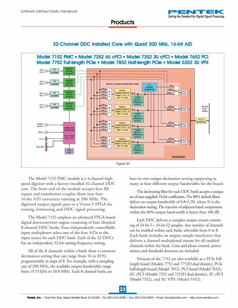
The Model 7152 PMC module is a 4-channel high-speed digitizer with a factory-installed 32-channel DDCcore. The front end of the module accepts four RFinputs and transformer-couples them into four16-bit A/D converters running at 200 MHz. Thedigitized output signals pass to a Virtex-5 FPGA forrouting, formatting and DDC signal processing.
The Model 7152 employs an advanced FPGA-baseddigital downconverter engine consisting of four identical8-channel DDC banks. Four independently controllableinput multiplexers select one of the four A/Ds as theinput source for each DDC bank. Each of the 32 DDCshas an independent 32-bit tuning frequency setting.
All of the 8 channels within a bank share a commondecimation setting that can range from 16 to 8192,programmable in steps of 8. For example, with a samplingrate of 200 MHz, the available output bandwidths rangefrom 19.53 kHz to 10.0 MHz. Each 8-channel bank can
have its own unique decimation setting supporting asmany as four different output bandwidths for the board.
The decimating filter for each DDC bank accepts a uniqueset of user-supplied 18-bit coefficients. The 80% default filtersdeliver an output bandwidth of 0.8*ƒs/N, where N is thedecimation setting. The rejection of adjacent-band componentswithin the 80% output band-width is better than 100 dB.
Each DDC delivers a complex output stream consist-ing of 24-bit I + 24-bit Q samples. Any number of channelscan be enabled within each bank, selectable from 0 to 8.Each bank includes an output sample interleaver thatdelivers a channel-multiplexed stream for all enabledchannels within the bank. Gain and phase control, powermeters and threshold detectors are included.
Versions of the 7152 are also available as a PCIe full-length board (Models 7752 and 7752D dual density), PCIehalf-length board (Model 7852), PCI board (Model 7652),6U cPCI (Models 7252 and 7252D dual density), 3U cPCI(Model 7352), and 3U VPX (Model 5352).
Model 7152 PMC Model 7152 PMC Model 7152 PMC Model 7152 PMC Model 7152 PMC ●●●●● Model 7252 6U cPCI Model 7252 6U cPCI Model 7252 6U cPCI Model 7252 6U cPCI Model 7252 6U cPCI ●●●●● Model 7352 3U cPCI Model 7352 3U cPCI Model 7352 3U cPCI Model 7352 3U cPCI Model 7352 3U cPCI ●●●●● Model 7652 PCI Model 7652 PCI Model 7652 PCI Model 7652 PCI Model 7652 PCIModel 7752 FModel 7752 FModel 7752 FModel 7752 FModel 7752 Full-length PCIe ull-length PCIe ull-length PCIe ull-length PCIe ull-length PCIe ●●●●● Model 7852 Half-length PCIe Model 7852 Half-length PCIe Model 7852 Half-length PCIe Model 7852 Half-length PCIe Model 7852 Half-length PCIe ●●●●● Model 5352 3U VPX Model 5352 3U VPX Model 5352 3U VPX Model 5352 3U VPX Model 5352 3U VPX
PPPPPentek, Inc.entek, Inc.entek, Inc.entek, Inc.entek, Inc. • One Park Way, Upper Saddle River, NJ 07458 • Tel: (201) 818-5900 • Fax: (201) 818-5904 • Email: [email protected] • http://www.pentek.com
2424242424
Software Defined Radio Handbook
PPPPProductsroductsroductsroductsroducts
Figure 35
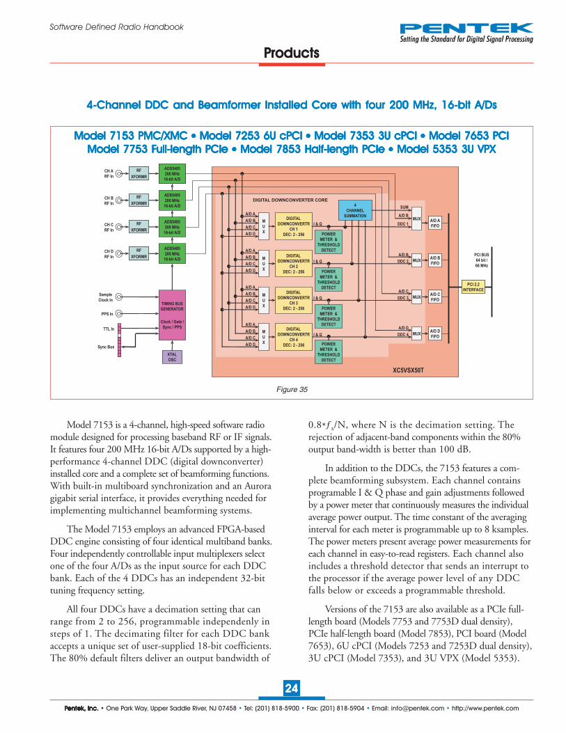
Model 7153 is a 4-channel, high-speed software radiomodule designed for processing baseband RF or IF signals.It features four 200 MHz 16-bit A/Ds supported by a high-performance 4-channel DDC (digital downconverter)installed core and a complete set of beamforming functions.With built-in multiboard synchronization and an Auroragigabit serial interface, it provides everything needed forimplementing multichannel beamforming systems.
The Model 7153 employs an advanced FPGA-basedDDC engine consisting of four identical multiband banks.Four independently controllable input multiplexers selectone of the four A/Ds as the input source for each DDCbank. Each of the 4 DDCs has an independent 32-bittuning frequency setting.
All four DDCs have a decimation setting that canrange from 2 to 256, programmable independenly insteps of 1. The decimating filter for each DDC bankaccepts a unique set of user-supplied 18-bit coefficients.The 80% default filters deliver an output bandwidth of
0.8*ƒs/N, where N is the decimation setting. Therejection of adjacent-band components within the 80%output band-width is better than 100 dB.
In addition to the DDCs, the 7153 features a com-plete beamforming subsystem. Each channel containsprogramable I & Q phase and gain adjustments followedby a power meter that continuously measures the individualaverage power output. The time constant of the averaginginterval for each meter is programmable up to 8 ksamples.The power meters present average power measurements foreach channel in easy-to-read registers. Each channel alsoincludes a threshold detector that sends an interrupt tothe processor if the average power level of any DDCfalls below or exceeds a programmable threshold.
Versions of the 7153 are also available as a PCIe full-length board (Models 7753 and 7753D dual density),PCIe half-length board (Model 7853), PCI board (Model7653), 6U cPCI (Models 7253 and 7253D dual density),3U cPCI (Model 7353), and 3U VPX (Model 5353).
.
RF
XFORMR
RF
XFORMR
AD6645
105 MHz
14-bit A/D
PCI 2.2
INTERFACE
MUXDIGITAL
DOWNCONVERTR
CH 1
DEC: 2 - 256
CH A
RF In
CH B
RF In
Sample
Clock In
Sync Bus
A/D A
A/D BI & Q
PCI BUS
64 bit /
66 MHz
DIGITAL DOWNCONVERTER CORE
XC5VSX50T
RF
XFORMR
RF
XFORMR
ADS5485
200 MHz
16-bit A/D
TIMING BUS
GENERATOR
Clock / Gate /
Sync / PPS
XTAL
OSC
PCI 2.2
INTERFACE
ADS5485
200 MHz
16-bit A/D
RF
XFORMR
CH C
RF In
RF
XFORMR
ADS5485
200 MHz
16-bit A/D
RF
XFORMR
CH D
RF In
RF
XFORMR
ADS5485
200 MHz
16-bit A/D
A/D C
A/D D
DDC 1
MUX
MUX
MUX
M
U
X
M
U
X
M
U
X
M
U
X
A/D A
FIFO
A/D B
FIFO
A/D C
FIFO
A/D D
FIFO
PPS In
TTL In
A/D A
A/D B
A/D C
A/D D
A/D A
A/D B
A/D C
A/D D
A/D A
A/D B
A/D C
A/D D
DIGITAL
DOWNCONVERTR
CH 2
DEC: 2 - 256
DIGITAL
DOWNCONVERTR
CH 3
DEC: 2 - 256
DIGITAL
DOWNCONVERTR
CH 4
DEC: 2 - 256
A/D B
DDC 2
A/D C
DDC 3
A/D D
DDC 4
4
CHANNEL
SUMMATION
POWER
METER &
THRESHOLD
DETECT
POWER
METER &
THRESHOLD
DETECT
POWER
METER &
THRESHOLD
DETECT
POWER
METER &
THRESHOLD
DETECT
A/D B
I & Q
I & Q
I & Q
SUM
4-4-4-4-4-Channel DDC and Beamformer Installed Core with four 200 MHz, 16-bit A/DsChannel DDC and Beamformer Installed Core with four 200 MHz, 16-bit A/DsChannel DDC and Beamformer Installed Core with four 200 MHz, 16-bit A/DsChannel DDC and Beamformer Installed Core with four 200 MHz, 16-bit A/DsChannel DDC and Beamformer Installed Core with four 200 MHz, 16-bit A/Ds
Model 7153 PMC/XMC Model 7153 PMC/XMC Model 7153 PMC/XMC Model 7153 PMC/XMC Model 7153 PMC/XMC ●●●●● Model 7253 6U cPCI Model 7253 6U cPCI Model 7253 6U cPCI Model 7253 6U cPCI Model 7253 6U cPCI ●●●●● Model 7353 3U cPCI Model 7353 3U cPCI Model 7353 3U cPCI Model 7353 3U cPCI Model 7353 3U cPCI ●●●●● Model 7653 PCI Model 7653 PCI Model 7653 PCI Model 7653 PCI Model 7653 PCIModel 7753 FModel 7753 FModel 7753 FModel 7753 FModel 7753 Full-length PCIe ull-length PCIe ull-length PCIe ull-length PCIe ull-length PCIe ●●●●● Model 7853 Half-length PCIe Model 7853 Half-length PCIe Model 7853 Half-length PCIe Model 7853 Half-length PCIe Model 7853 Half-length PCIe ●●●●● Model 5353 3U VPX Model 5353 3U VPX Model 5353 3U VPX Model 5353 3U VPX Model 5353 3U VPX

PPPPPentek, Inc.entek, Inc.entek, Inc.entek, Inc.entek, Inc. • One Park Way, Upper Saddle River, NJ 07458 • Tel: (201) 818-5900 • Fax: (201) 818-5904 • Email: [email protected] • http://www.pentek.com
2525252525
Software Defined Radio Handbook
PPPPProductsroductsroductsroductsroducts
Dual SDR TDual SDR TDual SDR TDual SDR TDual SDR Transceivers with 400 MHz A/D, 800 MHz D/A, and Virransceivers with 400 MHz A/D, 800 MHz D/A, and Virransceivers with 400 MHz A/D, 800 MHz D/A, and Virransceivers with 400 MHz A/D, 800 MHz D/A, and Virransceivers with 400 MHz A/D, 800 MHz D/A, and Virtex-5 FPGAstex-5 FPGAstex-5 FPGAstex-5 FPGAstex-5 FPGAs
Model 7156PMC/XMC
Model 7156 is a dual high-speed data convertersuitable for connection as the HF or IF input of acommunications system. It features two 400 MHz 14-bitA/Ds, a DUC with two 800 MHz 16-bit D/As, andtwo Virtex-5 FPGAs. Model 7156 uses the popularPMC format and supports the VITA 42 XMC standardfor switched fabric interfaces.
The Model 7156 architecture includes two Virtex-5FPGAs. The first FPGA is used primarily for signalprocessing while the second one is dedicated to boardinterfaces. All of the board’s data and control paths areaccessible by the FPGAs, enabling factory installedfunctions such as data multiplexing, channel selection, datapacking, gating, triggering and SDRAM memory control.
Two independent 512 MB banks of DDR2 SDRAMare available to the signal processing FPGA. Built-inmemory functions include an A/D data transient capturemode with pre- and post-triggering. All memory bankscan be easily accessed through the PCI-X interface.
A high-performance IP core wideband DDC may befactory-installed in the processing FPGA.
A 5-channel DMA controller and 64 bit/100 MHz PCI-Xinterface assures efficient transfers to and from the module.
Two 4X switched serial ports implemented with theXilinx Rocket I/O interfaces, connect the FPGA to theXMC connector with two 2.5 GB/sec data links to thecarrier board.
A dual bus system timing generator allows forsample clock synchronization to an external systemreference. It also supports large, multichannel appli-cations where the relative phases must be preserved.
Versions of the 7156 are also available as a PCIe full-length board (Models 7756 and 7756D dual density),PCIe half-length board (Model 7856), PCI board(Model 7656), 6U cPCI (Models 7256 and 7256D dualdensity), 3U cPCI (Model 7356), and 3U VPX (Model5356). All these products have similar features.
Figure 36
Model 7156 PMC/XMC Model 7156 PMC/XMC Model 7156 PMC/XMC Model 7156 PMC/XMC Model 7156 PMC/XMC ●●●●● Model 7256 6U cPCI Model 7256 6U cPCI Model 7256 6U cPCI Model 7256 6U cPCI Model 7256 6U cPCI ●●●●● Model 7356 3U cPCI Model 7356 3U cPCI Model 7356 3U cPCI Model 7356 3U cPCI Model 7356 3U cPCI ●●●●● Model 7656 PCI Model 7656 PCI Model 7656 PCI Model 7656 PCI Model 7656 PCIModel 7756 FModel 7756 FModel 7756 FModel 7756 FModel 7756 Full-length PCIe ull-length PCIe ull-length PCIe ull-length PCIe ull-length PCIe ●●●●● Model 7856 Half-length PCIe Model 7856 Half-length PCIe Model 7856 Half-length PCIe Model 7856 Half-length PCIe Model 7856 Half-length PCIe ●●●●● Model 5356 3U VPX Model 5356 3U VPX Model 5356 3U VPX Model 5356 3U VPX Model 5356 3U VPX
RF In
14
ADS5474
400 MHz
14-bit A/D
RF
XFORMR
RF In
14
ADS5474
400 MHz
14-bit A/D
RF
XFORMR
TIMING BUS
GENERATOR
Clock/ Sync /
Gate / PPS
Sample Clock In
TTL Gate / Trig
A/D Clock Bus
TTL Sync / PPS
Sample Clk
Sync Clk
Gate A
Gate B
Sync
PPS
PPS In
PROCESSING FPGA
VIRTEX –5: LX50T, SX50T, SX95T or FX100TTo All
Sections
Control/
Status
VCXO
GTP GTP GTP
INTERFACE FPGA
VIRTEX-5: LX30T, SX50T or FX70T
PCI-X BUS
(64 Bits
133 MHz)
P15 XMC
VITA 42.x
(PCIe, etc.)
P4 PMC
FPGA
I/O
64
32
4X
4X
4X4X
GTP
PCI-X GTP
1632 32
DDR 2
SDRAM
512 MB
DDR 2
SDRAM
512 MB
FLASH
32 MB
32
LVDS
LVDS
Timing Bus
D/A Clock Bus
32
RF
XFORMR
RF
XFORMR
RF Out RF Out
DIGITAL UPCONVERTER
800 MHz
16-bit D/A
800 MHz
16-bit D/A
64

PPPPPentek, Inc.entek, Inc.entek, Inc.entek, Inc.entek, Inc. • One Park Way, Upper Saddle River, NJ 07458 • Tel: (201) 818-5900 • Fax: (201) 818-5904 • Email: [email protected] • http://www.pentek.com
2626262626
Software Defined Radio Handbook
Model 7158 is a dual high-speed data convertersuitable for connection as the HF or IF input of acommunications system. It features two 500 MHz 12-bitA/Ds, a digital upconverter with two 800 MHz 16-bitD/As, and two Virtex-5 FPGAs. Model 7158 uses thepopular PMC format and supports the VITA 42 XMCstandard for switched fabric interfaces.
The Model 7158 architecture includes two Virtex-5FPGAs. The first FPGA is used primarily for signalprocessing while the second one is dedicated to boardinterfaces. All of the board’s data and control paths areaccessible by the FPGAs, enabling factory installedfunctions such as data multiplexing, channel selection, datapacking, gating, triggering and SDRAM memory control.
Two independent 256 MB banks of DDR2 SDRAMare available to the signal processing FPGA. Built-inmemory functions include an A/D data transient capturemode with pre- and post-triggering. All memory bankscan be easily accessed through the PCI-X interface.
A 5-channel DMA controller and 64 bit / 100 MHzPCI-X interface assures efficient transfers to and from themodule.
Two 4X switched serial ports implemented with theXilinx Rocket I/O interfaces, connect the FPGA to theXMC connector with two 2.5 GB/sec data links to thecarrier board.
A dual bus system timing generator allows forsample clock synchronization to an external systemreference. It also supports large, multichannel appli-cations where the relative phases must be preserved.
Versions of the 7158 are also available as a PCIe full-length board (Models 7758 and 7758D dual density),PCIe half-length board (Model 7858), PCI board(Model 7658), 6U cPCI (Models 7258 and 7258D dualdensity), 3U cPCI (Model 7358), and 3U VPX (Model5358). All these products have similar features.
Dual SDR TDual SDR TDual SDR TDual SDR TDual SDR Transceivers with 500 MHz A/D, 800 MHz D/A, and Virransceivers with 500 MHz A/D, 800 MHz D/A, and Virransceivers with 500 MHz A/D, 800 MHz D/A, and Virransceivers with 500 MHz A/D, 800 MHz D/A, and Virransceivers with 500 MHz A/D, 800 MHz D/A, and Virtex-5 FPGAstex-5 FPGAstex-5 FPGAstex-5 FPGAstex-5 FPGAs
Figure 37
PPPPProductsroductsroductsroductsroducts
Model 7158PMC/XMC
RF In
14
ADS5463
500 MHz
12-bit A/D
RF
XFORMR
RF In
14
ADS5463
500 MHz
12-bit A/D
RF
XFORMR
TIMING BUS
GENERATOR
Clock/ Sync /
Gate / PPS
Sample Clock /
Reference Clock In
TTL Gate / Trig
A/D Clock Bus
TTL Sync / PPS
Sample Clk
Sync Clk
Gate A
Gate B
Sync
PPS
PPS In
PROCESSING FPGA
VIRTEX –5: LX50T, LX155T, SX50T, SX95T or FX100TTo All
Sections
Control/
Status
VCXO
GTP GTP GTP
INTERFACE FPGA
VIRTEX-5: LX30T, SX50T or FX70T
PCI-X BUS
(64 Bits
100 MHz)
P15 XMC
VITA 42.x
(PCIe, etc.)
P4 PMC
FPGA
I/O
64
32
4X
4X
4X4X
GTP
PCI-X GTP
1632 32
DDR 2
SDRAM
256 MB
DDR 2
SDRAM
256 MB
FLASH
32 MB
32
LVDS
LVDS
Timing Bus
D/A Clock Bus
32
RF
XFORMR
RF
XFORMR
RF Out RF Out
DIGITAL UPCONVERTER
800 MHz
16-bit D/A
800 MHz
16-bit D/A
64
Model 7158 PMC/XMC Model 7158 PMC/XMC Model 7158 PMC/XMC Model 7158 PMC/XMC Model 7158 PMC/XMC ●●●●● Model 7258 6U cPCI Model 7258 6U cPCI Model 7258 6U cPCI Model 7258 6U cPCI Model 7258 6U cPCI ●●●●● Model 7358 3U cPCI Model 7358 3U cPCI Model 7358 3U cPCI Model 7358 3U cPCI Model 7358 3U cPCI ● ● ● ● ● Model 7658 PCIModel 7658 PCIModel 7658 PCIModel 7658 PCIModel 7658 PCIModel 7758 FModel 7758 FModel 7758 FModel 7758 FModel 7758 Full-length PCIe ull-length PCIe ull-length PCIe ull-length PCIe ull-length PCIe ●●●●● Model 7858 Half-length PCIe Model 7858 Half-length PCIe Model 7858 Half-length PCIe Model 7858 Half-length PCIe Model 7858 Half-length PCIe ●●●●● Model 5358 3U VPX Model 5358 3U VPX Model 5358 3U VPX Model 5358 3U VPX Model 5358 3U VPX
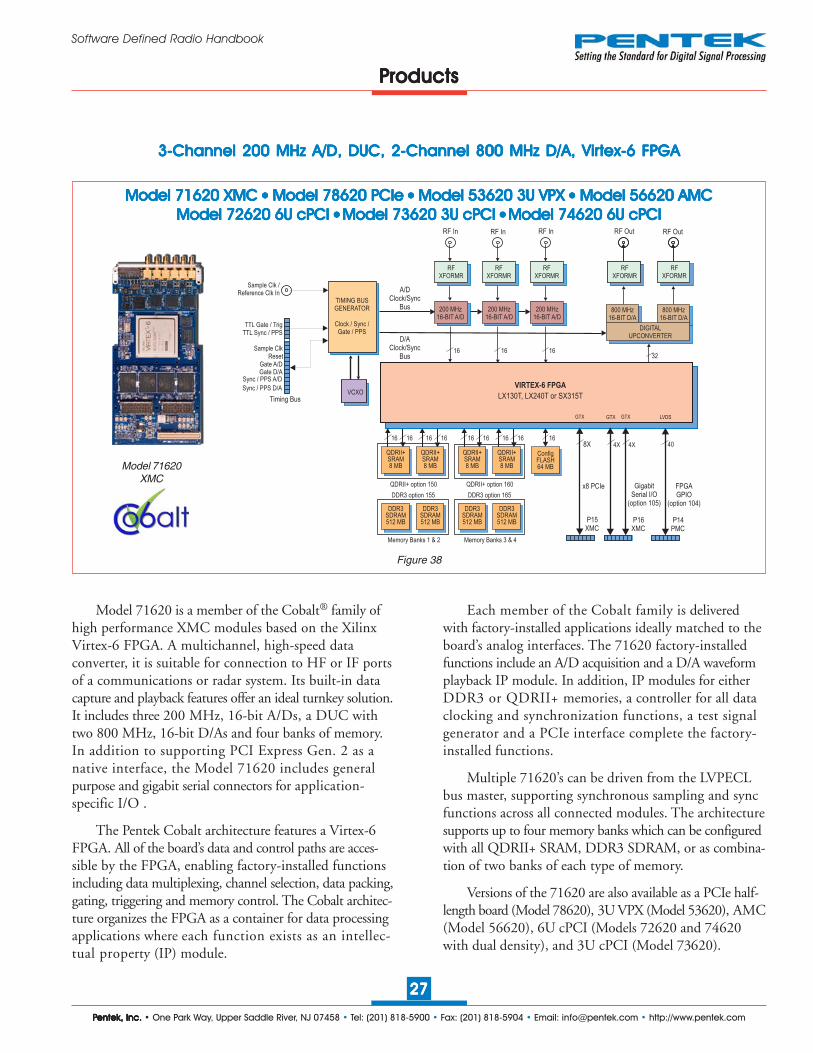
PPPPPentek, Inc.entek, Inc.entek, Inc.entek, Inc.entek, Inc. • One Park Way, Upper Saddle River, NJ 07458 • Tel: (201) 818-5900 • Fax: (201) 818-5904 • Email: [email protected] • http://www.pentek.com
2727272727
Software Defined Radio Handbook
3-3-3-3-3-Channel 200 MHz A/D, DUC, 2-Channel 200 MHz A/D, DUC, 2-Channel 200 MHz A/D, DUC, 2-Channel 200 MHz A/D, DUC, 2-Channel 200 MHz A/D, DUC, 2-Channel 800 MHz D/A, VirChannel 800 MHz D/A, VirChannel 800 MHz D/A, VirChannel 800 MHz D/A, VirChannel 800 MHz D/A, Virtex-6 FPGAtex-6 FPGAtex-6 FPGAtex-6 FPGAtex-6 FPGA
Model 71620 XMC Model 71620 XMC Model 71620 XMC Model 71620 XMC Model 71620 XMC ●●●●● Model 78620 PCIe Model 78620 PCIe Model 78620 PCIe Model 78620 PCIe Model 78620 PCIe ●●●●● Model 53620 3U VPX Model 53620 3U VPX Model 53620 3U VPX Model 53620 3U VPX Model 53620 3U VPX ●●●●● Model 56620 AMC Model 56620 AMC Model 56620 AMC Model 56620 AMC Model 56620 AMCModel 72620 6U cPCI Model 72620 6U cPCI Model 72620 6U cPCI Model 72620 6U cPCI Model 72620 6U cPCI ● ● ● ● ● Model 73620 3U cPCI Model 73620 3U cPCI Model 73620 3U cPCI Model 73620 3U cPCI Model 73620 3U cPCI ● ● ● ● ● Model 74620 6U cPCIModel 74620 6U cPCIModel 74620 6U cPCIModel 74620 6U cPCIModel 74620 6U cPCI
Figure 38
PPPPProductsroductsroductsroductsroducts
Model 71620XMC
TIMING BUSGENERATOR
Clock / Sync /Gate / PPS
VCXO
200 MHz16-BIT A/D
RFXFORMR
RFXFORMR
16
QDRII+SRAM8 MB
TTL Gate / TrigTTL Sync / PPS
Sample ClkReset
Gate A/DGate D/A
Sync / PPS A/D
Sync / PPS D/A
Timing Bus
200 MHz16-BIT A/D
Sample Clk /Reference Clk In
800 MHz16-BIT D/A
RFXFORMR
321616
RFXFORMR
16 16
ConfigFLASH64 MB
16
QDRII+SRAM8 MB
16
RFXFORMR
800 MHz16-BIT D/A
DIGITALUPCONVERTER
DDR3SDRAM512 MB
DDR3SDRAM512 MB
QDRII+ option 150
16
QDRII+SRAM8 MB
1616
QDRII+SRAM8 MB
16
DDR3SDRAM512 MB
DDR3SDRAM512 MB
RFXFORMR
200 MHz16-BIT A/D
16
Memory Banks 1 & 2 Memory Banks 3 & 4
DDR3 option 155
QDRII+ option 160
DDR3 option 165
RF In RF In RF In RF OutRF Out
D/AClock/Sync
Bus
A/DClock/Sync
Bus
RFXFORMR
40
GigabitSerial I/O
(option 105)
4X
GTX
4X
GTX LVDSGTX
FPGAGPIO
(option 104)
x8 PCIe
8X
P14PMC
P16XMC
P15XMC
VIRTEX-6 FPGA
LX130T, LX240T or SX315T
Model 71620 is a member of the Cobalt® family ofhigh performance XMC modules based on the XilinxVirtex-6 FPGA. A multichannel, high-speed dataconverter, it is suitable for connection to HF or IF portsof a communications or radar system. Its built-in datacapture and playback features offer an ideal turnkey solution.It includes three 200 MHz, 16-bit A/Ds, a DUC withtwo 800 MHz, 16-bit D/As and four banks of memory.In addition to supporting PCI Express Gen. 2 as anative interface, the Model 71620 includes generalpurpose and gigabit serial connectors for application-specific I/O .
The Pentek Cobalt architecture features a Virtex-6FPGA. All of the board’s data and control paths are acces-sible by the FPGA, enabling factory-installed functionsincluding data multiplexing, channel selection, data packing,gating, triggering and memory control. The Cobalt architec-ture organizes the FPGA as a container for data processingapplications where each function exists as an intellec-tual property (IP) module.
Each member of the Cobalt family is deliveredwith factory-installed applications ideally matched to theboard’s analog interfaces. The 71620 factory-installedfunctions include an A/D acquisition and a D/A waveformplayback IP module. In addition, IP modules for eitherDDR3 or QDRII+ memories, a controller for all dataclocking and synchronization functions, a test signalgenerator and a PCIe interface complete the factory-installed functions.
Multiple 71620’s can be driven from the LVPECLbus master, supporting synchronous sampling and syncfunctions across all connected modules. The architecturesupports up to four memory banks which can be configuredwith all QDRII+ SRAM, DDR3 SDRAM, or as combina-tion of two banks of each type of memory.
Versions of the 71620 are also available as a PCIe half-length board (Model 78620), 3U VPX (Model 53620), AMC(Model 56620), 6U cPCI (Models 72620 and 74620with dual density), and 3U cPCI (Model 73620).
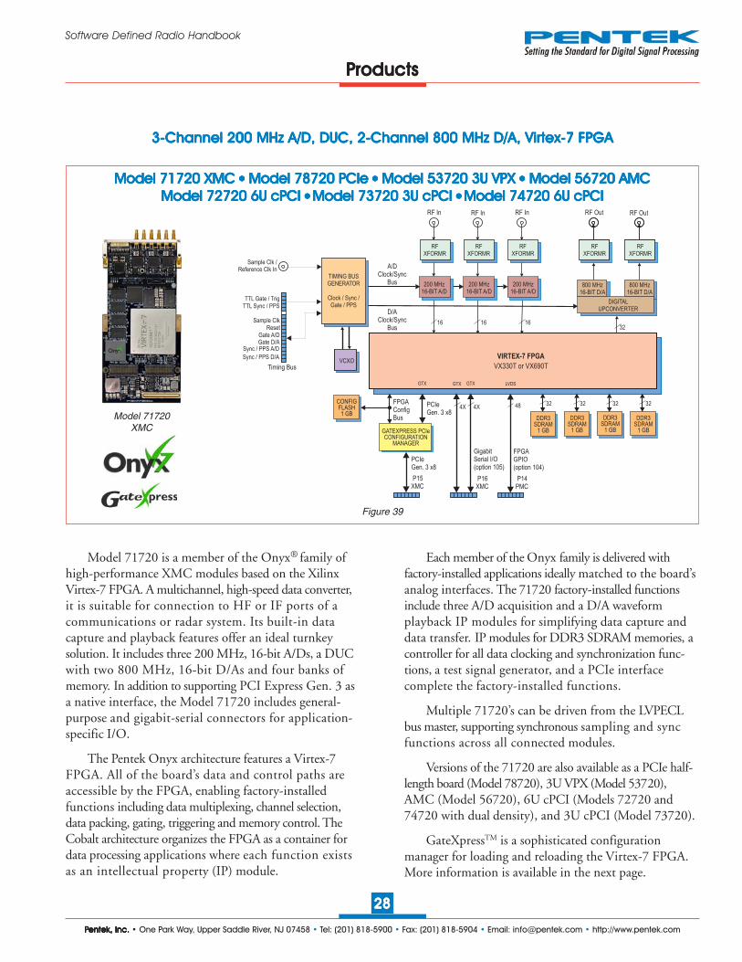
PPPPPentek, Inc.entek, Inc.entek, Inc.entek, Inc.entek, Inc. • One Park Way, Upper Saddle River, NJ 07458 • Tel: (201) 818-5900 • Fax: (201) 818-5904 • Email: [email protected] • http://www.pentek.com
2828282828
Software Defined Radio Handbook
3-3-3-3-3-Channel 200 MHz A/D, DUC, 2-Channel 200 MHz A/D, DUC, 2-Channel 200 MHz A/D, DUC, 2-Channel 200 MHz A/D, DUC, 2-Channel 200 MHz A/D, DUC, 2-Channel 800 MHz D/A, VirChannel 800 MHz D/A, VirChannel 800 MHz D/A, VirChannel 800 MHz D/A, VirChannel 800 MHz D/A, Virtex-7 FPGAtex-7 FPGAtex-7 FPGAtex-7 FPGAtex-7 FPGA
Model 71720 XMC Model 71720 XMC Model 71720 XMC Model 71720 XMC Model 71720 XMC ●●●●● Model 78720 PCIe Model 78720 PCIe Model 78720 PCIe Model 78720 PCIe Model 78720 PCIe ●●●●● Model 53720 3U VPX Model 53720 3U VPX Model 53720 3U VPX Model 53720 3U VPX Model 53720 3U VPX ●●●●● Model 56720 AMC Model 56720 AMC Model 56720 AMC Model 56720 AMC Model 56720 AMCModel 72720 6U cPCI Model 72720 6U cPCI Model 72720 6U cPCI Model 72720 6U cPCI Model 72720 6U cPCI ● ● ● ● ● Model 73720 3U cPCI Model 73720 3U cPCI Model 73720 3U cPCI Model 73720 3U cPCI Model 73720 3U cPCI ● ● ● ● ● Model 74720 6U cPCIModel 74720 6U cPCIModel 74720 6U cPCIModel 74720 6U cPCIModel 74720 6U cPCI
Figure 39
PPPPProductsroductsroductsroductsroducts
Model 71720XMC
TIMING BUSGENERATOR
Clock / Sync /Gate / PPS
VCXO
200 MHz16-BIT A/D
RFXFORMR
RFXFORMR
TTL Gate / TrigTTL Sync / PPS
Sample ClkReset
Gate A/DGate D/A
Sync / PPS A/D
Sync / PPS D/A
Timing Bus
200 MHz16-BIT A/D
Sample Clk /Reference Clk In
800 MHz16-BIT D/A
RFXFORMR
321616
RFXFORMR
RFXFORMR
800 MHz16-BIT D/A
DIGITALUPCONVERTER
RFXFORMR
200 MHz16-BIT A/D
16
RF In RF In RF In RF OutRF Out
D/AClock/Sync
Bus
A/DClock/Sync
Bus
RFXFORMR
GigabitSerial I/O(option 105)
GTXGTX LVDSGTX
FPGAGPIO(option 104)
PCIeGen. 3 x8
P14PMC
P16XMC
P15XMC
4X4X
VIRTEX-7 FPGA
VX330T or VX690T
CONFIGFLASH1 GB
DDR3SDRAM
1 GB
DDR3SDRAM
1 GB
DDR3SDRAM
1 GB
DDR3SDRAM
1 GB
48 32 32 32 32PCIeGen. 3 x8
FPGAConfigBus
GATEXPRESS PCIeCONFIGURATION
MANAGER
Model 71720 is a member of the Onyx® family ofhigh-performance XMC modules based on the XilinxVirtex-7 FPGA. A multichannel, high-speed data converter,it is suitable for connection to HF or IF ports of acommunications or radar system. Its built-in datacapture and playback features offer an ideal turnkeysolution. It includes three 200 MHz, 16-bit A/Ds, a DUCwith two 800 MHz, 16-bit D/As and four banks ofmemory. In addition to supporting PCI Express Gen. 3 asa native interface, the Model 71720 includes general-purpose and gigabit-serial connectors for application-specific I/O.
The Pentek Onyx architecture features a Virtex-7FPGA. All of the board’s data and control paths areaccessible by the FPGA, enabling factory-installedfunctions including data multiplexing, channel selection,data packing, gating, triggering and memory control. TheCobalt architecture organizes the FPGA as a container fordata processing applications where each function existsas an intellectual property (IP) module.
Each member of the Onyx family is delivered withfactory-installed applications ideally matched to the board’sanalog interfaces. The 71720 factory-installed functionsinclude three A/D acquisition and a D/A waveformplayback IP modules for simplifying data capture anddata transfer. IP modules for DDR3 SDRAM memories, acontroller for all data clocking and synchronization func-tions, a test signal generator, and a PCIe interfacecomplete the factory-installed functions.
Multiple 71720’s can be driven from the LVPECLbus master, supporting synchronous sampling and syncfunctions across all connected modules.
Versions of the 71720 are also available as a PCIe half-length board (Model 78720), 3U VPX (Model 53720),AMC (Model 56720), 6U cPCI (Models 72720 and74720 with dual density), and 3U cPCI (Model 73720).
GateXpressTM is a sophisticated configurationmanager for loading and reloading the Virtex-7 FPGA.More information is available in the next page.
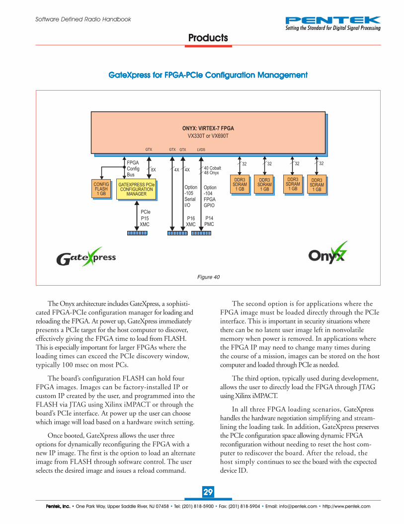
PPPPPentek, Inc.entek, Inc.entek, Inc.entek, Inc.entek, Inc. • One Park Way, Upper Saddle River, NJ 07458 • Tel: (201) 818-5900 • Fax: (201) 818-5904 • Email: [email protected] • http://www.pentek.com
2929292929
Software Defined Radio Handbook
GateXpress for FPGAGateXpress for FPGAGateXpress for FPGAGateXpress for FPGAGateXpress for FPGA-PCIe Configuration Management-PCIe Configuration Management-PCIe Configuration Management-PCIe Configuration Management-PCIe Configuration Management
Figure 40
PPPPProductsroductsroductsroductsroducts
ONYX: VIRTEX-7 FPGA
VX330T or VX690T
40 Cobalt48 Onyx
4X
GTX
4X8X
GTX LVDS
Option-104FPGAGPIO
Option-105SerialI/O
P14PMC
P16XMC
GTX
P15XMC
CONFIGFLASH1 GB
PCIe
FPGAConfigBus
GATEXPRESS PCIeCONFIGURATION
MANAGER
32 32 32 32
DDR3SDRAM
1 GB
DDR3SDRAM
1 GB
DDR3SDRAM
1 GB
DDR3SDRAM
1 GB
The Onyx architecture includes GateXpress, a sophisti-cated FPGA-PCIe configuration manager for loading andreloading the FPGA. At power up, GateXpress immediatelypresents a PCIe target for the host computer to discover,effectively giving the FPGA time to load from FLASH.This is especially important for larger FPGAs where theloading times can exceed the PCIe discovery window,typically 100 msec on most PCs.
The board’s configuration FLASH can hold fourFPGA images. Images can be factory-installed IP orcustom IP created by the user, and programmed into theFLASH via JTAG using Xilinx iMPACT or through theboard’s PCIe interface. At power up the user can choosewhich image will load based on a hardware switch setting.
Once booted, GateXpress allows the user threeoptions for dynamically reconfiguring the FPGA with anew IP image. The first is the option to load an alternateimage from FLASH through software control. The userselects the desired image and issues a reload command.
The second option is for applications where theFPGA image must be loaded directly through the PCIeinterface. This is important in security situations wherethere can be no latent user image left in nonvolatilememory when power is removed. In applications wherethe FPGA IP may need to change many times duringthe course of a mission, images can be stored on the hostcomputer and loaded through PCIe as needed.
The third option, typically used during development,allows the user to directly load the FPGA through JTAGusing Xilinx iMPACT.
In all three FPGA loading scenarios, GateXpresshandles the hardware negotiation simplifying and stream-lining the loading task. In addition, GateXpress preservesthe PCIe configuration space allowing dynamic FPGAreconfiguration without needing to reset the host com-puter to rediscover the board. After the reload, thehost simply continues to see the board with the expecteddevice ID.
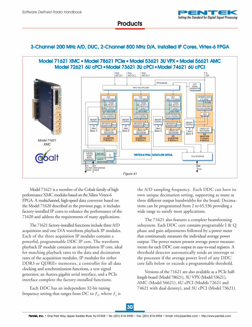
PPPPPentek, Inc.entek, Inc.entek, Inc.entek, Inc.entek, Inc. • One Park Way, Upper Saddle River, NJ 07458 • Tel: (201) 818-5900 • Fax: (201) 818-5904 • Email: [email protected] • http://www.pentek.com
3030303030
Software Defined Radio Handbook
PCIe INTERFACE
fromA/D Ch 1
fromA/D Ch 2
fromA/D Ch 3
PCIe
8Xfrom previousboard
to nextboard
sum out
sum in
VIRTEX-6 FPGA DATAFLOW DETAILVIRTEX-6 FPGA DATAFLOW DETAIL
A/DACQUISITIONIP MODULE 1
A/DACQUISITIONIP MODULE 2
A/DACQUISITIONIP MODULE 3
LINKED-LISTDMA ENGINE
LINKED-LISTDMA ENGINE
LINKED-LISTDMA ENGINE
METADATAGENERATOR
METADATAGENERATOR
METADATAGENERATORto
MemBank 1
MEMORYCONTROL
toMem
Bank 2
MEMORYCONTROL
toMem
Bank 3
MEMORYCONTROL
MUX MUX MUX
DATA PACKING &FLOW CONTROL
DATA PACKING &FLOW CONTROL
DATA PACKING &FLOW CONTROL
AURORAGIGABITSERIAL
INTERFACE
INPUT MULTIPLEXER
�
SUMMER
DDCDEC: 2 TO 65536
DDCDEC: 2 TO 65536
BEAMFORMER CORE
DDCDEC: 2 TO 65536
POWERMETER &
THRESHOLDDETECT
POWERMETER &
THRESHOLDDETECT
POWERMETER &
THRESHOLDDETECT
MUXDDC CORE DDC CORE DDC CORE
D/AWAVEFORMPLAYBACKIP MODULE
toD/A
D/A loopbackTEST
SIGNALGENERATOR
MUX
LINKED-LISTDMA ENGINE
toMem
Bank 4
MEMORYCONTROL
DATA PACKING &FLOW CONTROL
DATA UNPACKING& FLOW CONTROL
INTERPOLATOR2 TO 65536
IP CORE
8X4X 4X
3-3-3-3-3-Channel 200 MHz A/D, DUC, 2-Channel 200 MHz A/D, DUC, 2-Channel 200 MHz A/D, DUC, 2-Channel 200 MHz A/D, DUC, 2-Channel 200 MHz A/D, DUC, 2-Channel 800 MHz D/A, Installed IP Cores, VirChannel 800 MHz D/A, Installed IP Cores, VirChannel 800 MHz D/A, Installed IP Cores, VirChannel 800 MHz D/A, Installed IP Cores, VirChannel 800 MHz D/A, Installed IP Cores, Virtex-6 FPGAtex-6 FPGAtex-6 FPGAtex-6 FPGAtex-6 FPGA
Model 71621 XMC Model 71621 XMC Model 71621 XMC Model 71621 XMC Model 71621 XMC ●●●●● Model 78621 PCIe Model 78621 PCIe Model 78621 PCIe Model 78621 PCIe Model 78621 PCIe ●●●●● Model 53621 3U VPX Model 53621 3U VPX Model 53621 3U VPX Model 53621 3U VPX Model 53621 3U VPX ●●●●● Model 56621 AMC Model 56621 AMC Model 56621 AMC Model 56621 AMC Model 56621 AMCModel 72621 6U cPCI Model 72621 6U cPCI Model 72621 6U cPCI Model 72621 6U cPCI Model 72621 6U cPCI ● ● ● ● ● Model 73621 3U cPCI Model 73621 3U cPCI Model 73621 3U cPCI Model 73621 3U cPCI Model 73621 3U cPCI ● ● ● ● ● Model 74621 6U cPCIModel 74621 6U cPCIModel 74621 6U cPCIModel 74621 6U cPCIModel 74621 6U cPCI
Figure 41
Model 71621XMC
PPPPProductsroductsroductsroductsroducts
Model 71621 is a member of the Cobalt family of highperformance XMC modules based on the Xilinx Virtex-6FPGA. A multichannel, high-speed data converter based onthe Model 71620 described in the previous page, it includesfactory-installed IP cores to enhance the performance of the71620 and address the requirements of many applications.
The 71621 factory-installed functions include three A/Dacquisition and one D/A waveform playback IP modules.Each of the three acquisition IP modules contains apowerful, programmable DDC IP core. The waveformplayback IP module contains an interpolation IP core, idealfor matching playback rates to the data and decimationrates of the acquisition modules. IP modules for eitherDDR3 or QDRII+ memories, a controller for all dataclocking and synchronization functions, a test signalgenerator, an Aurora gigabit serial interface, and a PCIeinterface complete the factory-installed functions.
Each DDC has an independent 32-bit tuningfrequency setting that ranges from DC to ƒs, where ƒs is
the A/D sampling frequency. Each DDC can have itsown unique decimation setting, supporting as many asthree different output bandwidths for the board. Decima-tions can be programmed from 2 to 65,536 providing awide range to satisfy most applications.
The 71621 also features a complete beamformingsubsystem. Each DDC core contains programable I & Qphase and gain adjustments followed by a power meterthat continuously measures the individual average poweroutput. The power meters present average power measure-ments for each DDC core output in easy-to-read registers. Athreshold detector automatically sends an interrupt tothe processor if the average power level of any DDCcore falls below or exceeds a programmable threshold.
Versions of the 71621 are also available as a PCIe half-length board (Model 78621), 3U VPX (Model 53621),AMC (Model 56621), 6U cPCI (Models 72621 and74621 with dual density), and 3U cPCI (Model 73621).

PPPPPentek, Inc.entek, Inc.entek, Inc.entek, Inc.entek, Inc. • One Park Way, Upper Saddle River, NJ 07458 • Tel: (201) 818-5900 • Fax: (201) 818-5904 • Email: [email protected] • http://www.pentek.com
3131313131
Software Defined Radio Handbook
1 GHz A/D, 1 GHz D/A, Vir1 GHz A/D, 1 GHz D/A, Vir1 GHz A/D, 1 GHz D/A, Vir1 GHz A/D, 1 GHz D/A, Vir1 GHz A/D, 1 GHz D/A, Virtex-6 FPGAtex-6 FPGAtex-6 FPGAtex-6 FPGAtex-6 FPGA
Model 78630 PCIe Model 78630 PCIe Model 78630 PCIe Model 78630 PCIe Model 78630 PCIe ● ● ● ● ● Model 71630 XMC Model 71630 XMC Model 71630 XMC Model 71630 XMC Model 71630 XMC ●●●●● Model 53630 3U VPX Model 53630 3U VPX Model 53630 3U VPX Model 53630 3U VPX Model 53630 3U VPX ● ● ● ● ● Model 56630 XMCModel 56630 XMCModel 56630 XMCModel 56630 XMCModel 56630 XMCModel 72630 6U cPCI Model 72630 6U cPCI Model 72630 6U cPCI Model 72630 6U cPCI Model 72630 6U cPCI ● ● ● ● ● Model 73630 3U cPCI Model 73630 3U cPCI Model 73630 3U cPCI Model 73630 3U cPCI Model 73630 3U cPCI ● ● ● ● ● Model 74630 6U cPCIModel 74630 6U cPCIModel 74630 6U cPCIModel 74630 6U cPCIModel 74630 6U cPCI
Figure 42
PPPPProductsroductsroductsroductsroducts
Model 78630x8 PCIe
TIMING BUSGENERATOR
Clock / Sync /Gate / PPS D/A Clock/Sync Bus
VCXO
16
QDRII+SRAM8 MB
Gate InSync In
A/D Sync Bus
Sample Clk /Reference Clk In
A/D Clock/Sync Bus
16
16 16
ConfigFLASH64 MB
16
QDRII+SRAM8 MB
16
RFXFORMR
RF Out
RFXFORMR
DDR3SDRAM512 MB
DDR3SDRAM512 MB
QDRII+ option 150
16 1616 16
DDR3SDRAM512 MB
DDR3SDRAM512 MB
RF In
RFXFORMR
1 GHz12-BIT A/D
12
Memory Banks 1 & 2 Memory Banks 3 & 4DDR3 option 155 DDR3 option 165
Gate InSync In
D/A Sync Bus
1 GHz16-BIT D/A
TTLPPS/Gate/Sync
40 4X
GTX
4X
GTXLVDS GTX
OptionalFPGAGPIO
OptionalSerialI/O
8X
68-pinHeader
x8 PCI Express
Dual 4XSerialConn
x8 PCIe
VIRTEX-6 FPGA
LX130T, LX240T or SX315T
Model 78630 is a member of the Cobalt family of highperformance PCIe boards based on the Xilinx Virtex-6FPGA. A high-speed data converter, it is suitable forconnection to HF or IF ports of a communications or radarsystem. Its built-in data capture and playback features offeran ideal turnkey solution as well as a platform for develop-ing and deploying custom FPGA processing IP. It includes1 GHz, 12-bit A/D, 1 GHz, 16-bit D/A converters andfour banks of memory. In addition to supporting PCIExpress Gen. 2 as a native interface, the Model 78630includes optional general purpose and gigabit serial cardconnectors for application- specific I/O protocols.
The Pentek Cobalt architecture features a Virtex-6FPGA. All of the board’s data and control paths are acces-sible by the FPGA, enabling factory-installed functionsincluding data multiplexing, channel selection, data packing,gating, triggering and memory control. The Cobalt architec-ture organizes the FPGA as a container for data process-ing applications where each function exists as an intellec-tual property (IP) module.
Each member of the Cobalt family is deliveredwith factory-installed applications ideally matched to theboard’s analog interfaces. The 78630 factory-installedfunctions include an A/D acquisition and a D/A waveformplayback IP module. In addition, IP modules for eitherDDR3 or QDRII+ memories, a controller for all dataclocking and synchronization functions, a test signalgenerator and a PCIe interface complete the factory-installed functions.
Multiple 78630’s can be driven from the LVPECLbus master, supporting synchronous sampling and syncfunctions across all connected boards. The architecturesupports up to four memory banks which can be configuredwith all QDRII+ SRAM, DDR3 SDRAM, or as combina-tion of two banks of each type of memory.
Versions of the 78630 are also available as an XMCmodule (Model 71630), 3U VPX (Model 53630), AMC(Model 56630), 6U cPCI (Models 72630 and 74630with dual density), and 3U cPCI (Model 73630).

PPPPPentek, Inc.entek, Inc.entek, Inc.entek, Inc.entek, Inc. • One Park Way, Upper Saddle River, NJ 07458 • Tel: (201) 818-5900 • Fax: (201) 818-5904 • Email: [email protected] • http://www.pentek.com
3232323232
Software Defined Radio Handbook
Figure 43
PPPPProductsroductsroductsroductsroducts
TIMING BUSGENERATOR
Clock / Sync /Gate / PPS
32
Gate In
Reset In
Sync Bus
Sample Clk
A/D Clock/Sync Bus
16
ConfigFLASH64 MB
32
DDR3SDRAM512 MB
DDR3SDRAM512 MB
3232
DDR3SDRAM512 MB
DDR3SDRAM512 MB
RF In
RFXFORMR
3.6 GHz (1 Channel)or
1.8 GHz (2 Channel)12-bit A/D
12
Memory Banks 1 & 2 Memory Banks 3 & 4
TTLPPS/Gate/Sync
RF In
RFXFORMR
Ref Clk In
Ref Clk Out 12
Block Diagram, Model 72640
Model 74640 doubles all resources
except the PCI-to-PCI Bridge
VIRTEX-6 FPGA
MODEL 73640
INTERFACES ONLY
PCIeto PCI
BRIDGE
40
LVDS GTX
OptionalFPGA I/O(Option -104)
PCI/PCI-X BUS32-bit, 33/66 MHz
J2
PCIeto PCI
BRIDGE
PCIto PCI
BRIDGE
From/To OtherXMC Module ofMODEL 74640
GTX
x4 PCIe
PCI/PCI-X BUS32/64-bit, 33/66 MHz
4X40
LVDS
OptionalFPGA I/O(Option -104)
J3
VIRTEX-6 FPGA
LX130T, LX240T or SX315T
Model 74640Dual Density
Model 73640Single Density
Model 72640 6U cPCI Model 72640 6U cPCI Model 72640 6U cPCI Model 72640 6U cPCI Model 72640 6U cPCI ● ● ● ● ● Model 73640 3U cPCI Model 73640 3U cPCI Model 73640 3U cPCI Model 73640 3U cPCI Model 73640 3U cPCI ● ● ● ● ● Model 74640 6U cPCIModel 74640 6U cPCIModel 74640 6U cPCIModel 74640 6U cPCIModel 74640 6U cPCIModel 71640 XMC Model 71640 XMC Model 71640 XMC Model 71640 XMC Model 71640 XMC ●●●●● Model 78640 PCIe Model 78640 PCIe Model 78640 PCIe Model 78640 PCIe Model 78640 PCIe ●●●●● Model 53640 3U VPX Model 53640 3U VPX Model 53640 3U VPX Model 53640 3U VPX Model 53640 3U VPX ●●●●● Model 56640 AMC Model 56640 AMC Model 56640 AMC Model 56640 AMC Model 56640 AMC
1- or 2-1- or 2-1- or 2-1- or 2-1- or 2-Channel 3.6 GHz and 2- or 4-Channel 3.6 GHz and 2- or 4-Channel 3.6 GHz and 2- or 4-Channel 3.6 GHz and 2- or 4-Channel 3.6 GHz and 2- or 4-Channel 1.8 GHz, 12-bit A/D, VirChannel 1.8 GHz, 12-bit A/D, VirChannel 1.8 GHz, 12-bit A/D, VirChannel 1.8 GHz, 12-bit A/D, VirChannel 1.8 GHz, 12-bit A/D, Virtex-6 FPGAtex-6 FPGAtex-6 FPGAtex-6 FPGAtex-6 FPGA
Models 72640, 73640 and 74640 are membersof the Cobalt family of high performance CompactPCIboards based on the Xilinx Virtex-6 FPGA. Theyconsist of one or two Model 71640 XMC modulesmounted on a cPCI carrier board. These models include oneor two 3.6 GHz, 12-bit A/D converters and four or eightbanks of memory.
The Pentek Cobalt architecture features a Virtex-6FPGA. All of the board’s data and control paths areaccessible by the FPGA, enabling factory-installedfunctions including data multiplexing, channel selec-tion, data packing, gating, triggering and memory control.The Cobalt architecture organizes the FPGA as a containerfor data processing applications where each function existsas an intellectual property (IP) module.
Each member of the Cobalt family is deliveredwith factory-installed applications ideally matched to theboard’s analog interfaces. The factory-installed functions ofthese models include one or two A/D acquisition IP
modules. In addition, IP modules for DDR3 memories,controllers for all data clocking and synchronizationfunctions, a test signal generator and a PCIe interfacecomplete the factory-installed functions.
The front end accepts analog HF or IF inputs ona pair of front panel SSMC connectors with transformercoupling into a Texas Instruments ADC12D1800 12-bitA/D. The converter operates in single-channel inter-leaved mode with a sampling rate of 3.6 GHz and aninput bandwidth of 1.75 GHz; or, in dual-channel modewith a sampling rate of 1.8 GHz and input bandwidth of2.8 GHz. The ADC12D1800 provides a programmable15-bit gain adjustment allowing these models to have a fullscale input range of +2 dBm to +4 dBm.
Model 72640 is a 6U cPCI board, while Model73640 is a 3U cPCI board; Model 74640 is a dualdensity 6U cPCI board. Also available is an XMC module(Model 71640), PCIe half-length board (Model 78640), 3UVPX (Model 53640), and AMC (Model 56640).
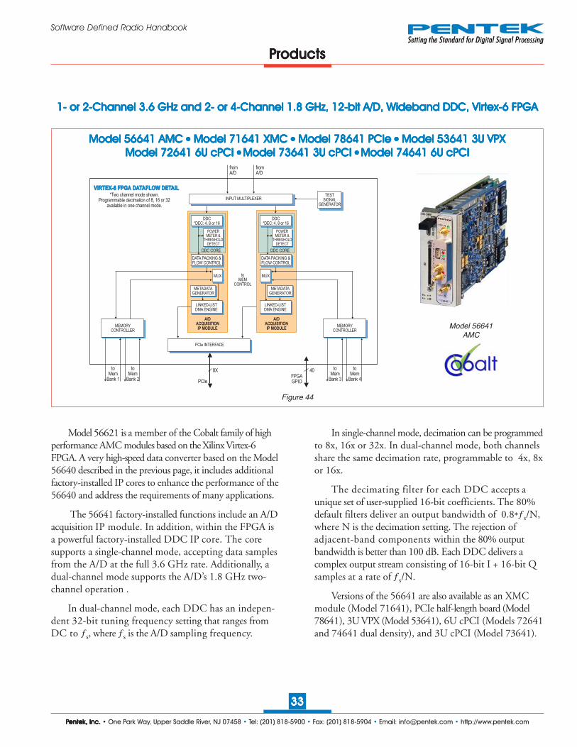
PPPPPentek, Inc.entek, Inc.entek, Inc.entek, Inc.entek, Inc. • One Park Way, Upper Saddle River, NJ 07458 • Tel: (201) 818-5900 • Fax: (201) 818-5904 • Email: [email protected] • http://www.pentek.com
3333333333
Software Defined Radio Handbook
Figure 44
PPPPProductsroductsroductsroductsroducts
Model 56641 AMC Model 56641 AMC Model 56641 AMC Model 56641 AMC Model 56641 AMC ●●●●● Model 71641 XMC Model 71641 XMC Model 71641 XMC Model 71641 XMC Model 71641 XMC ●●●●● Model 78641 PCIe Model 78641 PCIe Model 78641 PCIe Model 78641 PCIe Model 78641 PCIe ●●●●● Model 53641 3U VPX Model 53641 3U VPX Model 53641 3U VPX Model 53641 3U VPX Model 53641 3U VPXModel 72641 6U cPCI Model 72641 6U cPCI Model 72641 6U cPCI Model 72641 6U cPCI Model 72641 6U cPCI ● ● ● ● ● Model 73641 3U cPCI Model 73641 3U cPCI Model 73641 3U cPCI Model 73641 3U cPCI Model 73641 3U cPCI ● ● ● ● ● Model 74641 6U cPCIModel 74641 6U cPCIModel 74641 6U cPCIModel 74641 6U cPCIModel 74641 6U cPCI
1- or 2-1- or 2-1- or 2-1- or 2-1- or 2-Channel 3.6 GHz and 2- or 4-Channel 3.6 GHz and 2- or 4-Channel 3.6 GHz and 2- or 4-Channel 3.6 GHz and 2- or 4-Channel 3.6 GHz and 2- or 4-Channel 1.8 GHz, 12-bit A/D, WChannel 1.8 GHz, 12-bit A/D, WChannel 1.8 GHz, 12-bit A/D, WChannel 1.8 GHz, 12-bit A/D, WChannel 1.8 GHz, 12-bit A/D, Wideband DDC, Virideband DDC, Virideband DDC, Virideband DDC, Virideband DDC, Virtex-6 FPGAtex-6 FPGAtex-6 FPGAtex-6 FPGAtex-6 FPGA
PCIe INTERFACE
fromA/D
PCIeFPGAGPIO
VIRTEX-6 FPGA DATAFLOW DETAILVIRTEX-6 FPGA DATAFLOW DETAIL
A/DACQUISITIONIP MODULE
MUX
INPUT MULTIPLEXERTEST
SIGNALGENERATOR
MEMORYCONTROLLER
8X 40toMem
Bank 2
toMem
Bank 1
fromA/D
LINKED-LISTDMA ENGINE
toMEM
CONTROL
MEMORYCONTROLLER
toMem
Bank 4
toMem
Bank 3
*Two channel mode shown.Programmable decimation of 8, 16 or 32
available in one channel mode.
DDC*DEC: 4, 8 or 16
POWERMETER &
THRESHOLDDETECT
DDC CORE
DATA PACKING &FLOW CONTROL
A/DACQUISITIONIP MODULE
MUX
LINKED-LISTDMA ENGINE
DDC*DEC: 4, 8 or 16
POWERMETER &
THRESHOLDDETECT
DDC CORE
DATA PACKING &FLOW CONTROL
METADATAGENERATOR
METADATAGENERATOR
Model 56641AMC
Model 56621 is a member of the Cobalt family of highperformance AMC modules based on the Xilinx Virtex-6FPGA. A very high-speed data converter based on the Model56640 described in the previous page, it includes additionalfactory-installed IP cores to enhance the performance of the56640 and address the requirements of many applications.
The 56641 factory-installed functions include an A/Dacquisition IP module. In addition, within the FPGA isa powerful factory-installed DDC IP core. The coresupports a single-channel mode, accepting data samplesfrom the A/D at the full 3.6 GHz rate. Additionally, adual-channel mode supports the A/D’s 1.8 GHz two-channel operation .
In dual-channel mode, each DDC has an indepen-dent 32-bit tuning frequency setting that ranges fromDC to ƒs, where ƒs is the A/D sampling frequency.
In single-channel mode, decimation can be programmedto 8x, 16x or 32x. In dual-channel mode, both channelsshare the same decimation rate, programmable to 4x, 8xor 16x.
The decimating filter for each DDC accepts aunique set of user-supplied 16-bit coefficients. The 80%default filters deliver an output bandwidth of 0.8*ƒs/N,where N is the decimation setting. The rejection ofadjacent-band components within the 80% outputbandwidth is better than 100 dB. Each DDC delivers acomplex output stream consisting of 16-bit I + 16-bit Qsamples at a rate of ƒs/N.
Versions of the 56641 are also available as an XMCmodule (Model 71641), PCIe half-length board (Model78641), 3U VPX (Model 53641), 6U cPCI (Models 72641and 74641 dual density), and 3U cPCI (Model 73641).

PPPPPentek, Inc.entek, Inc.entek, Inc.entek, Inc.entek, Inc. • One Park Way, Upper Saddle River, NJ 07458 • Tel: (201) 818-5900 • Fax: (201) 818-5904 • Email: [email protected] • http://www.pentek.com
3434343434
Software Defined Radio Handbook
2-2-2-2-2-Channel 500 MHz A/D, DUC, 2-Channel 500 MHz A/D, DUC, 2-Channel 500 MHz A/D, DUC, 2-Channel 500 MHz A/D, DUC, 2-Channel 500 MHz A/D, DUC, 2-Channel 800 MHz D/A, VirChannel 800 MHz D/A, VirChannel 800 MHz D/A, VirChannel 800 MHz D/A, VirChannel 800 MHz D/A, Virtex-6 FPGAtex-6 FPGAtex-6 FPGAtex-6 FPGAtex-6 FPGA
Model 53650 3U VPX Model 53650 3U VPX Model 53650 3U VPX Model 53650 3U VPX Model 53650 3U VPX ●●●●● Model 71650 XMC Model 71650 XMC Model 71650 XMC Model 71650 XMC Model 71650 XMC ● ● ● ● ● Model 78650 PCIe Model 78650 PCIe Model 78650 PCIe Model 78650 PCIe Model 78650 PCIe ●●●●● Model 56650 AMC Model 56650 AMC Model 56650 AMC Model 56650 AMC Model 56650 AMCModel 72650 6U cPCI Model 72650 6U cPCI Model 72650 6U cPCI Model 72650 6U cPCI Model 72650 6U cPCI ● ● ● ● ● Model 73650 3U cPCI Model 73650 3U cPCI Model 73650 3U cPCI Model 73650 3U cPCI Model 73650 3U cPCI ●●●●● Model 74650 6U cPCI Model 74650 6U cPCI Model 74650 6U cPCI Model 74650 6U cPCI Model 74650 6U cPCI
Figure 45
Model 53650 3U VPXCOTS and rugged
PPPPProductsroductsroductsroductsroducts
D/AClock/Sync
Bus
VCXO
500 MHz12-BIT A/D
RF In
RFXFORMR
RF In
RFXFORMR
16
QDRII+SRAM8 MB
TTL Gate / Trig
TTL Sync / PPS
Sample Clk
Reset
Gate A/D
Gate D/A
Sync / PPS A/D
Sync / PPS D/A
Timing Bus
500 MHz12-BIT A/D
Sample Clk /Reference Clk In A/D
Clock/SyncBus 800 MHz
16-BIT D/A
RFXFORMR
321616
RF Out
RFXFORMR
16 16
ConfigFLASH64 MB
16
QDRII+SRAM8 MB
16
RFXFORMR
RF Out
RFXFORMR
800 MHz16-BIT D/A
DIGITALUPCONVERTER
DDR3SDRAM512 MB
DDR3SDRAM512 MB
QDRII+ option 150
16
QDRII+SRAM8 MB
1616
QDRII+SRAM8 MB
16
DDR3SDRAM512 MB
DDR3SDRAM512 MB
Memory Banks 1 & 2 Memory Banks 3 & 4
DDR3 option 155
QDRII+ option 160
DDR3 option 165
TTLPPS/Gate/Sync
40
GigabitSerial I/O
(option 105)
4X
GTX
4X
GTX LVDSGTX
FPGAGPIO
(option 104)
x8 PCIe
8X
P14PMC
P16XMC
P15XMC
TIMING BUSGENERATOR
Clock / Sync /Gate / PPS
VIRTEX-6 FPGA
LX130T, LX240T or SX315T
Model 53650 is a member of the Cobalt family ofhigh performance 3U VPX boards based on the XilinxVirtex-6 FPGA. A two-channel, high-speed dataconverter, it is suitable for connection to HF or IF portsof a communications or radar system. Its built-in datacapture and playback features offer an ideal turnkeysolution as well as a platform for developing and deployingcustom FPGA processing IP. The 53650 includes two500 MHz 12-bit A/Ds, one DUC, two 800 MHz 16-bitD/As and four banks of memory. It features built-insupport for PCI Express over the 3U VPX backplane.
The Pentek Cobalt architecture features a Virtex-6FPGA. All of the board’s data and control paths are acces-sible by the FPGA, enabling factory-installed functionsincluding data multiplexing, channel selection, data packing,gating, triggering and memory control. The Cobalt architec-ture organizes the FPGA as a container for data process-ing applications where each function exists as an intellec-tual property (IP) module.
Each member of the Cobalt family is deliveredwith factory-installed applications ideally matched to theboard’s analog interfaces. The 53650 factory-installedfunctions include an A/D acquisition and a D/A waveformplayback IP module. In addition, IP modules for eitherDDR3 or QDRII+ memories, a controller for all dataclocking and synchronization functions, a test signalgenerator and a PCIe interface complete the factory-installed functions.
Multiple 53650’s can be driven from the LVPECLbus master, supporting synchronous sampling and syncfunctions across all connected boards. The architecturesupports up to four memory banks which can be configuredwith all QDRII+ SRAM, DDR3 SDRAM, or as combina-tion of two banks of each type of memory.
Versions of the 53650 are also available as an XMCmodule (Model 71650), as a PCIe half-length board (Model78650), AMC (Model 56650), 6U cPCI (Models 72650and 74650 with dual density), and 3U cPCI (Model 73650).
This Model is alsoavailable with 400 MHz,
14-bit A/Ds

PPPPPentek, Inc.entek, Inc.entek, Inc.entek, Inc.entek, Inc. • One Park Way, Upper Saddle River, NJ 07458 • Tel: (201) 818-5900 • Fax: (201) 818-5904 • Email: [email protected] • http://www.pentek.com
3535353535
Software Defined Radio Handbook
Model 72651 6U cPCI Model 72651 6U cPCI Model 72651 6U cPCI Model 72651 6U cPCI Model 72651 6U cPCI ● ● ● ● ● Model 73651 3U cPCI Model 73651 3U cPCI Model 73651 3U cPCI Model 73651 3U cPCI Model 73651 3U cPCI ● ● ● ● ● Model 74651 6U cPCIModel 74651 6U cPCIModel 74651 6U cPCIModel 74651 6U cPCIModel 74651 6U cPCIModel 53651 3U VPX Model 53651 3U VPX Model 53651 3U VPX Model 53651 3U VPX Model 53651 3U VPX ● ● ● ● ● Model 71651 XMC Model 71651 XMC Model 71651 XMC Model 71651 XMC Model 71651 XMC ●●●●● Model 78651 PCIe Model 78651 PCIe Model 78651 PCIe Model 78651 PCIe Model 78651 PCIe ●●●●● Model 56651 AMC Model 56651 AMC Model 56651 AMC Model 56651 AMC Model 56651 AMC
PPPPProductsroductsroductsroductsroducts
2- or 4-2- or 4-2- or 4-2- or 4-2- or 4-Channel 500 MHz A/D, with DDCs, DUCs, 2- or 4-Channel 500 MHz A/D, with DDCs, DUCs, 2- or 4-Channel 500 MHz A/D, with DDCs, DUCs, 2- or 4-Channel 500 MHz A/D, with DDCs, DUCs, 2- or 4-Channel 500 MHz A/D, with DDCs, DUCs, 2- or 4-Channel 800 MHz D/A, VirChannel 800 MHz D/A, VirChannel 800 MHz D/A, VirChannel 800 MHz D/A, VirChannel 800 MHz D/A, Virtex-6 FPGAtex-6 FPGAtex-6 FPGAtex-6 FPGAtex-6 FPGA
Figure 46
PCIe INTERFACE
fromA/D Ch 1
fromA/D Ch 2
PCIe
4Xfrom previousboard
to nextboard
sum out
sum in
VIRTEX-6 FPGA DATAFLOW DETAILVIRTEX-6 FPGA DATAFLOW DETAIL
A/DACQUISITIONIP MODULE 1
A/DACQUISITIONIP MODULE 2
LINKED-LISTDMA ENGINE
LINKED-LISTDMA ENGINE
METADATAGENERATOR
METADATAGENERATORto
MemBank 1
MEMORYCONTROL
toMem
Bank 2
MEMORYCONTROL
MUX MUX
DATA PACKING &FLOW CONTROL
DATA PACKING &FLOW CONTROL
AURORAGIGABITSERIAL
INTERFACE
INPUT MULTIPLEXER
�SUMMER
DDCDEC: 2 TO 131027
DDCDEC: 2 TO 131027
BEAMFORMER CORE
POWERMETER &
THRESHOLDDETECT
POWERMETER &
THRESHOLDDETECT
MUXDDC CORE DDC CORE
D/AWAVEFORMPLAYBACKIP MODULE
toD/A
D/A loopbackTEST
SIGNALGENERATOR
MUX
LINKED-LISTDMA ENGINE
toMem
Bank 4
MEMORYCONTROL
DATA UNPACKING& FLOW CONTROL
INTERPOLATOR2 TO 65536
IP CORE
4X 4X
Model 74651Dual Density
Model 73651Single Density
Models 72651, 73651 and 74651 are members ofthe Cobalt family of high performance CompactPCI boardsbased on the Xilinx Virtex-6 FPGA. They consist ofone or two Model 71651 XMC modules mounted on acPCI carrier board. These models include two or four A/Ds,two or four multiband DDCs, one ot two DUCs, twoor four D/As and three or six banks of memory.
These models feature two or four A/D Acquisition IPmodules for easily capturing and moving data. Eachmodule can receive data from either of the two A/Ds, atest signal generator or from the D/A Waveform PlaybackIP module in loopback mode.
Within each A/D Acquisition IP Module is apowerful DDC IP core. Because of the flexible inputrouting of the A/D Acquisition IP Modules, many differentconfigurations can be achieved including one A/D drivingboth DDCs or each of the two A/Ds driving its own DDC.
Each DDC has an independent 32-bit tuningfrequency setting that ranges from DC to ƒs, where ƒs is
the A/D sampling frequency. Each DDC can have itsown unique decimation setting, supporting as many astwo or four different output bandwidths for the board.Decimations can be programmed from 2 to 131,072providing a wide range to satisfy most applications.
In addition to the DDCs, these models feature oneor two complete beamforming subsystems. Each DDCcore contains programable I & Q phase and gain adjust-ments followed by a power meter that continuouslymeasures the individual average power output. The timeconstant of the averaging interval for each meter is program-mable up to 8K samples. The power meters present averagepower measurements for each DDC core output in easy-to-read registers.
Model 72651 is a 6U cPCI board, while Model73651 is a 3U cPCI board; Model 74651 is a dualdensity 6U cPCI board. Also available is an XMC module(Model 71651), PCIe half-length board (Model 78651), 3UVPX (Model 53651), and AMC (Model 56651).

PPPPPentek, Inc.entek, Inc.entek, Inc.entek, Inc.entek, Inc. • One Park Way, Upper Saddle River, NJ 07458 • Tel: (201) 818-5900 • Fax: (201) 818-5904 • Email: [email protected] • http://www.pentek.com
3636363636
Software Defined Radio Handbook
PPPPProductsroductsroductsroductsroducts
Figure 47
4-4-4-4-4-Channel 200 MHz 16-bit A/D with VirChannel 200 MHz 16-bit A/D with VirChannel 200 MHz 16-bit A/D with VirChannel 200 MHz 16-bit A/D with VirChannel 200 MHz 16-bit A/D with Virtex-6 FPGAtex-6 FPGAtex-6 FPGAtex-6 FPGAtex-6 FPGA
Model 71660 XMC Model 71660 XMC Model 71660 XMC Model 71660 XMC Model 71660 XMC ●●●●● Model 78660 PCIe Model 78660 PCIe Model 78660 PCIe Model 78660 PCIe Model 78660 PCIe ●●●●● Model 53660 3U VPX Model 53660 3U VPX Model 53660 3U VPX Model 53660 3U VPX Model 53660 3U VPX ●●●●● Model 56660 AMC Model 56660 AMC Model 56660 AMC Model 56660 AMC Model 56660 AMCModel 72660 6U cPCI Model 72660 6U cPCI Model 72660 6U cPCI Model 72660 6U cPCI Model 72660 6U cPCI ● ● ● ● ● Model 73660 3U cPCI Model 73660 3U cPCI Model 73660 3U cPCI Model 73660 3U cPCI Model 73660 3U cPCI ● ● ● ● ● Model 74660 6U cPCIModel 74660 6U cPCIModel 74660 6U cPCIModel 74660 6U cPCIModel 74660 6U cPCI
Model 71660XMC
TIMING BUSGENERATOR
Clock / Sync /Gate / PPS
VCXO
200 MHz16-BIT A/D
RF In
RFXFORMR
RF In
RFXFORMR
16
QDRII+SRAM8 MB
TTL Gate / TrigTTL Sync / PPS
Sample ClkReset
Gate AGate B
Sync / PPS A
Sync / PPS B
Timing Bus
200 MHz16-BIT A/D
Sample Clk /Reference Clk In
A/D Clock/Sync Bus
1616
16 16
ConfigFLASH64 MB
16
QDRII+SRAM8 MB
16
DDR3SDRAM512 MB
DDR3SDRAM512 MB
QDRII+ option 150
16
QDRII+SRAM8 MB
1616
QDRII+SRAM8 MB
16
DDR3SDRAM512 MB
DDR3SDRAM512 MB
RF In
RFXFORMR
200 MHz16-BIT A/D
16
Memory Banks 1 & 2 Memory Banks 3 & 4
DDR3 option 155
QDRII+ option 160
DDR3 option 165
RF In
RFXFORMR
200 MHz16-BIT A/D
16
Gate / Trigger /Sync / PPS
40
GigabitSerial I/O
(option 105)
4X
GTX
4X
GTX LVDSGTX
FPGAGPIO
(option 104)
x8 PCIe
8X
P14PMC
P16XMC
P15XMC
VIRTEX-6 FPGA
LX130T, LX240T or SX315T
Model 71660 is a member of the Cobalt family ofhigh performance XMC modules based on the XilinxVirtex-6 FPGA. A multichannel, high-speed dataconverter, it is suitable for connection to HF or IF portsof a communications or radar system. Its built-in datacapture and playback features offer an ideal turnkey solutionas well as a platform for developing and deploying customFPGA processing IP. It includes four 200 MHz, 16-bit A/Dsand four banks of memory. In addition to supportingPCI Express Gen. 2 as a native interface, the Model71660 includes general purpose and gigabit serial connec-tors for application-specific I/O .
The Pentek Cobalt architecture features a Virtex-6FPGA. All of the board’s data and control paths are acces-sible by the FPGA, enabling factory-installed functionsincluding data multiplexing, channel selection, data packing,gating, triggering and memory control. The Cobalt architec-ture organizes the FPGA as a container for data processingapplications where each function exists as an intellec-tual property (IP) module.
Each member of the Cobalt family is deliveredwith factory-installed applications ideally matched to theboard’s analog interfaces. The 71660 factory-installedfunctions include four A/D acquisition IP modules. Inaddition, IP modules for either DDR3 or QDRII+memories, a controller for all data clocking and syn-chronization functions, a test signal generator and aPCIe interface complete the factory-installed functions.
Multiple 71660’s can be driven from the LVPECLbus master, supporting synchronous sampling and syncfunctions across all connected modules. The architecturesupports up to four memory banks which can be configuredwith all QDRII+ SRAM, DDR3 SDRAM, or as combina-tion of two banks of each type of memory.
Versions of the 71660 are also available as a PCIe half-length board (Model 78660), 3U VPX (Model 53660),AMC (Model 56660), 6U cPCI (Models 72660 and74660 with dual density), and 3U cPCI (Model 73660).
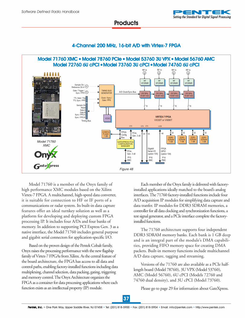
PPPPPentek, Inc.entek, Inc.entek, Inc.entek, Inc.entek, Inc. • One Park Way, Upper Saddle River, NJ 07458 • Tel: (201) 818-5900 • Fax: (201) 818-5904 • Email: [email protected] • http://www.pentek.com
3737373737
Software Defined Radio Handbook
4-4-4-4-4-Channel 200 MHz, 16-bit A/D with VirChannel 200 MHz, 16-bit A/D with VirChannel 200 MHz, 16-bit A/D with VirChannel 200 MHz, 16-bit A/D with VirChannel 200 MHz, 16-bit A/D with Virtex-7 FPGAtex-7 FPGAtex-7 FPGAtex-7 FPGAtex-7 FPGA
Model 71760 XMC Model 71760 XMC Model 71760 XMC Model 71760 XMC Model 71760 XMC ●●●●● Model 78760 PCIe Model 78760 PCIe Model 78760 PCIe Model 78760 PCIe Model 78760 PCIe ●●●●● Model 53760 3U VPX Model 53760 3U VPX Model 53760 3U VPX Model 53760 3U VPX Model 53760 3U VPX ●●●●● Model 56760 AMC Model 56760 AMC Model 56760 AMC Model 56760 AMC Model 56760 AMCModel 72760 6U cPCI Model 72760 6U cPCI Model 72760 6U cPCI Model 72760 6U cPCI Model 72760 6U cPCI ● ● ● ● ● Model 73760 3U cPCI Model 73760 3U cPCI Model 73760 3U cPCI Model 73760 3U cPCI Model 73760 3U cPCI ● ● ● ● ● Model 74760 6U cPCIModel 74760 6U cPCIModel 74760 6U cPCIModel 74760 6U cPCIModel 74760 6U cPCI
Figure 48
PPPPProductsroductsroductsroductsroducts
Model 71760XMC
TIMING BUSGENERATOR
Clock / Sync /Gate / PPS
VCXO
200 MHz16-BIT A/D
RF In
RFXFORMR
RF In
RFXFORMR
VIRTEX-7 FPGA
VX330T or VX690T
TTL Gate / TrigTTL Sync / PPS
Sample ClkReset
Gate AGate B
Sync / PPS A
Sync / PPS B
Timing Bus
200 MHz16-BIT A/D
Sample Clk /Reference Clk In
A/D Clock/Sync Bus
1616
RF In
RFXFORMR
200 MHz16-BIT A/D
16
RF In
RFXFORMR
200 MHz16-BIT A/D
16
Gate / Trigger /Sync / PPS
GigabitSerial I/O(option 105)
GTXGTX LVDSGTX
FPGAGPIO(option 104)
PCIeGen. 3 x8
P14PMC
P16XMC
P15XMC
4X4XCONFIGFLASH1 GB
DDR3SDRAM
1 GB
DDR3SDRAM
1 GB
DDR3SDRAM
1 GB
DDR3SDRAM
1 GB
48 32 32 32 32PCIeGen. 3 x8
FPGAConfigBus
GATEXPRESS PCIeCONFIGURATION
MANAGER
Model 71760 is a member of the Onyx family ofhigh performance XMC modules based on the XilinxVirtex-7 FPGA. A multichannel, high-speed data converter,it is suitable for connection to HF or IF ports of acommunications or radar system. Its built-in data capturefeatures offer an ideal turnkey solution as well as aplatform for developing and deploying custom FPGAprocessing IP. It includes four A/Ds and four banks ofmemory. In addition to supporting PCI Express Gen. 3 as anative interface, the Model 71760 includes general purposeand gigabit serial connectors for application-specific I/O.
Based on the proven design of the Pentek Cobalt family,Onyx raises the processing performance with the new flagshipfamily of Virtex-7 FPGAs from Xilinx. As the central feature ofthe board architecture, the FPGA has access to all data andcontrol paths, enabling factory-installed functions including datamultiplexing, channel selection, data packing, gating, triggeringand memory control. The Onyx Architecture organizes theFPGA as a container for data processing applications where eachfunction exists as an intellectual property (IP) module.
Each member of the Onyx family is delivered with factory-installed applications ideally matched to the board’s analoginterfaces. The 71760 factory-installed functions include fourA/D acquisition IP modules for simplifying data capture anddata tranfer. IP modules for DDR3 SDRAM memories, acontroller for all data clocking and synchronization functions, atest signal generator, and a PCIe interface complete the factory-installed functions.
The 71760 architecture supports four independentDDR3 SDRAM memory banks. Each bank is 1 GB deepand is an integral part of the module’s DMA capabili-ties, providing FIFO memory space for creating DMApackets. Built-in memory functions include multichannelA/D data capture, tagging and streaming.
Versions of the 71760 are also available as a PCIe half-length board (Model 78760), 3U VPX (Model 53760),AMC (Model 56760), 6U cPCI (Models 72760 and74760 dual density), and 3U cPCI (Model 73760).
Please go to page 29 for information about GateXpress.
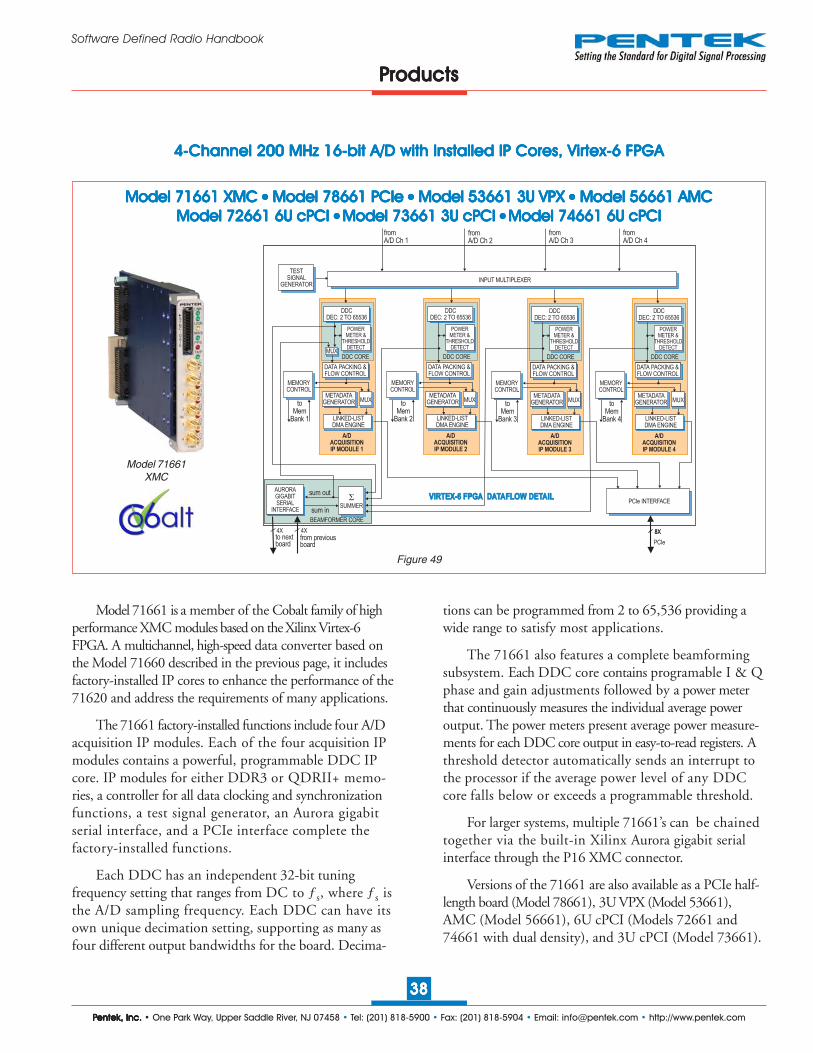
PPPPPentek, Inc.entek, Inc.entek, Inc.entek, Inc.entek, Inc. • One Park Way, Upper Saddle River, NJ 07458 • Tel: (201) 818-5900 • Fax: (201) 818-5904 • Email: [email protected] • http://www.pentek.com
3838383838
Software Defined Radio Handbook
PPPPProductsroductsroductsroductsroducts
Figure 49
4-4-4-4-4-Channel 200 MHz 16-bit A/D with Installed IP Cores, VirChannel 200 MHz 16-bit A/D with Installed IP Cores, VirChannel 200 MHz 16-bit A/D with Installed IP Cores, VirChannel 200 MHz 16-bit A/D with Installed IP Cores, VirChannel 200 MHz 16-bit A/D with Installed IP Cores, Virtex-6 FPGAtex-6 FPGAtex-6 FPGAtex-6 FPGAtex-6 FPGA
Model 71661 XMC Model 71661 XMC Model 71661 XMC Model 71661 XMC Model 71661 XMC ●●●●● Model 78661 PCIe Model 78661 PCIe Model 78661 PCIe Model 78661 PCIe Model 78661 PCIe ●●●●● Model 53661 3U VPX Model 53661 3U VPX Model 53661 3U VPX Model 53661 3U VPX Model 53661 3U VPX ●●●●● Model 56661 AMC Model 56661 AMC Model 56661 AMC Model 56661 AMC Model 56661 AMCModel 72661 6U cPCI Model 72661 6U cPCI Model 72661 6U cPCI Model 72661 6U cPCI Model 72661 6U cPCI ● ● ● ● ● Model 73661 3U cPCI Model 73661 3U cPCI Model 73661 3U cPCI Model 73661 3U cPCI Model 73661 3U cPCI ● ● ● ● ● Model 74661 6U cPCIModel 74661 6U cPCIModel 74661 6U cPCIModel 74661 6U cPCIModel 74661 6U cPCI
Model 71661XMC
BEAMFORMER CORE
PCIe INTERFACE
fromA/D Ch 1
fromA/D Ch 2
fromA/D Ch 3
fromA/D Ch 4
PCIe
8Xfrom previousboard
to nextboard
sum out
sum in
VIRTEX-6 FPGA DATAFLOW DETAILVIRTEX-6 FPGA DATAFLOW DETAIL
A/DACQUISITIONIP MODULE 1
A/DACQUISITIONIP MODULE 2
A/DACQUISITIONIP MODULE 3
A/DACQUISITIONIP MODULE 4
LINKED-LISTDMA ENGINE
LINKED-LISTDMA ENGINE
LINKED-LISTDMA ENGINE
LINKED-LISTDMA ENGINE
METADATAGENERATOR
METADATAGENERATOR
METADATAGENERATOR
METADATAGENERATORto
MemBank 1
MEMORYCONTROL
toMem
Bank 2
MEMORYCONTROL
toMem
Bank 3
toMem
Bank 4
MEMORYCONTROL
MEMORYCONTROL
MUX MUX MUX MUX
DATA PACKING &FLOW CONTROL
DATA PACKING &FLOW CONTROL
DATA PACKING &FLOW CONTROL
DATA PACKING &FLOW CONTROL
AURORAGIGABITSERIAL
INTERFACE
INPUT MULTIPLEXER
�
SUMMER
DDCDEC: 2 TO 65536
DDCDEC: 2 TO 65536
DDCDEC: 2 TO 65536
DDCDEC: 2 TO 65536
POWERMETER &
THRESHOLDDETECT
POWERMETER &
THRESHOLDDETECT
POWERMETER &
THRESHOLDDETECT
POWERMETER &
THRESHOLDDETECT
MUXDDC CORE DDC CORE DDC CORE DDC CORE
TESTSIGNAL
GENERATOR
DATA PACKING &FLOW CONTROL
DATA PACKING &FLOW CONTROL
8X4X 4X
Model 71661 is a member of the Cobalt family of highperformance XMC modules based on the Xilinx Virtex-6FPGA. A multichannel, high-speed data converter based onthe Model 71660 described in the previous page, it includesfactory-installed IP cores to enhance the performance of the71620 and address the requirements of many applications.
The 71661 factory-installed functions include four A/Dacquisition IP modules. Each of the four acquisition IPmodules contains a powerful, programmable DDC IPcore. IP modules for either DDR3 or QDRII+ memo-ries, a controller for all data clocking and synchronizationfunctions, a test signal generator, an Aurora gigabitserial interface, and a PCIe interface complete thefactory-installed functions.
Each DDC has an independent 32-bit tuningfrequency setting that ranges from DC to ƒs, where ƒs isthe A/D sampling frequency. Each DDC can have itsown unique decimation setting, supporting as many asfour different output bandwidths for the board. Decima-
tions can be programmed from 2 to 65,536 providing awide range to satisfy most applications.
The 71661 also features a complete beamformingsubsystem. Each DDC core contains programable I & Qphase and gain adjustments followed by a power meterthat continuously measures the individual average poweroutput. The power meters present average power measure-ments for each DDC core output in easy-to-read registers. Athreshold detector automatically sends an interrupt tothe processor if the average power level of any DDCcore falls below or exceeds a programmable threshold.
For larger systems, multiple 71661’s can be chainedtogether via the built-in Xilinx Aurora gigabit serialinterface through the P16 XMC connector.
Versions of the 71661 are also available as a PCIe half-length board (Model 78661), 3U VPX (Model 53661),AMC (Model 56661), 6U cPCI (Models 72661 and74661 with dual density), and 3U cPCI (Model 73661).
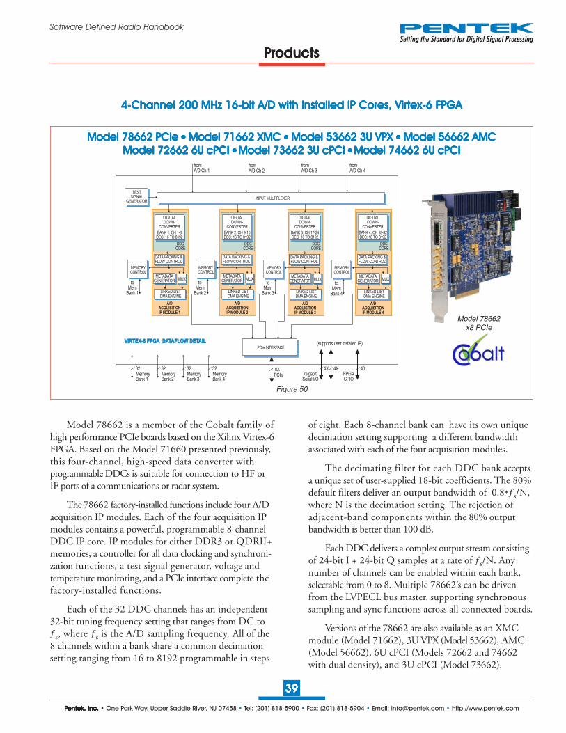
PPPPPentek, Inc.entek, Inc.entek, Inc.entek, Inc.entek, Inc. • One Park Way, Upper Saddle River, NJ 07458 • Tel: (201) 818-5900 • Fax: (201) 818-5904 • Email: [email protected] • http://www.pentek.com
3939393939
Software Defined Radio Handbook
Figure 50
PPPPProductsroductsroductsroductsroducts
4-4-4-4-4-Channel 200 MHz 16-bit A/D with Installed IP Cores, VirChannel 200 MHz 16-bit A/D with Installed IP Cores, VirChannel 200 MHz 16-bit A/D with Installed IP Cores, VirChannel 200 MHz 16-bit A/D with Installed IP Cores, VirChannel 200 MHz 16-bit A/D with Installed IP Cores, Virtex-6 FPGAtex-6 FPGAtex-6 FPGAtex-6 FPGAtex-6 FPGA
Model 78662 PCIe Model 78662 PCIe Model 78662 PCIe Model 78662 PCIe Model 78662 PCIe ●●●●● Model 71662 XMC Model 71662 XMC Model 71662 XMC Model 71662 XMC Model 71662 XMC ●●●●● Model 53662 3U VPX Model 53662 3U VPX Model 53662 3U VPX Model 53662 3U VPX Model 53662 3U VPX ●●●●● Model 56662 AMC Model 56662 AMC Model 56662 AMC Model 56662 AMC Model 56662 AMCModel 72662 6U cPCI Model 72662 6U cPCI Model 72662 6U cPCI Model 72662 6U cPCI Model 72662 6U cPCI ● ● ● ● ● Model 73662 3U cPCI Model 73662 3U cPCI Model 73662 3U cPCI Model 73662 3U cPCI Model 73662 3U cPCI ● ● ● ● ● Model 74662 6U cPCIModel 74662 6U cPCIModel 74662 6U cPCIModel 74662 6U cPCIModel 74662 6U cPCI
Model 78662 is a member of the Cobalt family ofhigh performance PCIe boards based on the Xilinx Virtex-6FPGA. Based on the Model 71660 presented previously,this four-channel, high-speed data converter withprogrammable DDCs is suitable for connection to HF orIF ports of a communications or radar system.
The 78662 factory-installed functions include four A/Dacquisition IP modules. Each of the four acquisition IPmodules contains a powerful, programmable 8-channelDDC IP core. IP modules for either DDR3 or QDRII+memories, a controller for all data clocking and synchroni-zation functions, a test signal generator, voltage andtemperature monitoring, and a PCIe interface complete thefactory-installed functions.
Each of the 32 DDC channels has an independent32-bit tuning frequency setting that ranges from DC toƒs, where ƒs is the A/D sampling frequency. All of the8 channels within a bank share a common decimationsetting ranging from 16 to 8192 programmable in steps
of eight. Each 8-channel bank can have its own uniquedecimation setting supporting a different bandwidthassociated with each of the four acquisition modules.
The decimating filter for each DDC bank acceptsa unique set of user-supplied 18-bit coefficients. The 80%default filters deliver an output bandwidth of 0.8*ƒs/N,where N is the decimation setting. The rejection ofadjacent-band components within the 80% outputbandwidth is better than 100 dB.
Each DDC delivers a complex output stream consistingof 24-bit I + 24-bit Q samples at a rate of ƒs/N. Anynumber of channels can be enabled within each bank,selectable from 0 to 8. Multiple 78662’s can be drivenfrom the LVPECL bus master, supporting synchronoussampling and sync functions across all connected boards.
Versions of the 78662 are also available as an XMCmodule (Model 71662), 3U VPX (Model 53662), AMC(Model 56662), 6U cPCI (Models 72662 and 74662with dual density), and 3U cPCI (Model 73662).
Model 78662x8 PCIe
fromA/D Ch 1
fromA/D Ch 2
fromA/D Ch 3
fromA/D Ch 4
VIRTEX-6 FPGA DATAFLOW DETAILVIRTEX-6 FPGA DATAFLOW DETAIL
A/DACQUISITIONIP MODULE 1
A/DACQUISITIONIP MODULE 2
A/DACQUISITIONIP MODULE 3
A/DACQUISITIONIP MODULE 4
LINKED-LISTDMA ENGINE
LINKED-LISTDMA ENGINE
METADATAGENERATOR
METADATAGENERATOR
METADATAGENERATOR
METADATAGENERATORto
MemBank 1
MEMORYCONTROL
toMem
Bank 2
MEMORYCONTROL
toMem
Bank 3
toMem
Bank 4
MEMORYCONTROL
MEMORYCONTROL
MUX MUX MUX MUX
DATA PACKING &FLOW CONTROL
DATA PACKING &FLOW CONTROL
DATA PACKING &FLOW CONTROL
DATA PACKING &FLOW CONTROL
INPUT MULTIPLEXER
TESTSIGNAL
GENERATOR
DATA PACKING &FLOW CONTROL
DATA PACKING &FLOW CONTROL
DDCCORE
DIGITALDOWN-
CONVERTER
BANK 1: CH 1-8DEC: 16 TO 8192
.
DDCCORE
DIGITALDOWN-
CONVERTER
BANK 2: CH 9-16DEC: 16 TO 8192
.
DDCCORE
DIGITALDOWN-
CONVERTER
BANK 3: CH 17-24DEC: 16 TO 8192
.
DDCCORE
DIGITALDOWN-
CONVERTER
BANK 4: CH 18-32DEC: 16 TO 8192
.
MemoryBank 4
PCIe INTERFACE
PCIe8X
LINKED-LISTDMA ENGINE
LINKED-LISTDMA ENGINE
GigabitSerial I/O
FPGAGPIO
(supports user installed IP)
4X 4X 4032MemoryBank 3
32MemoryBank 2
32MemoryBank 1
32
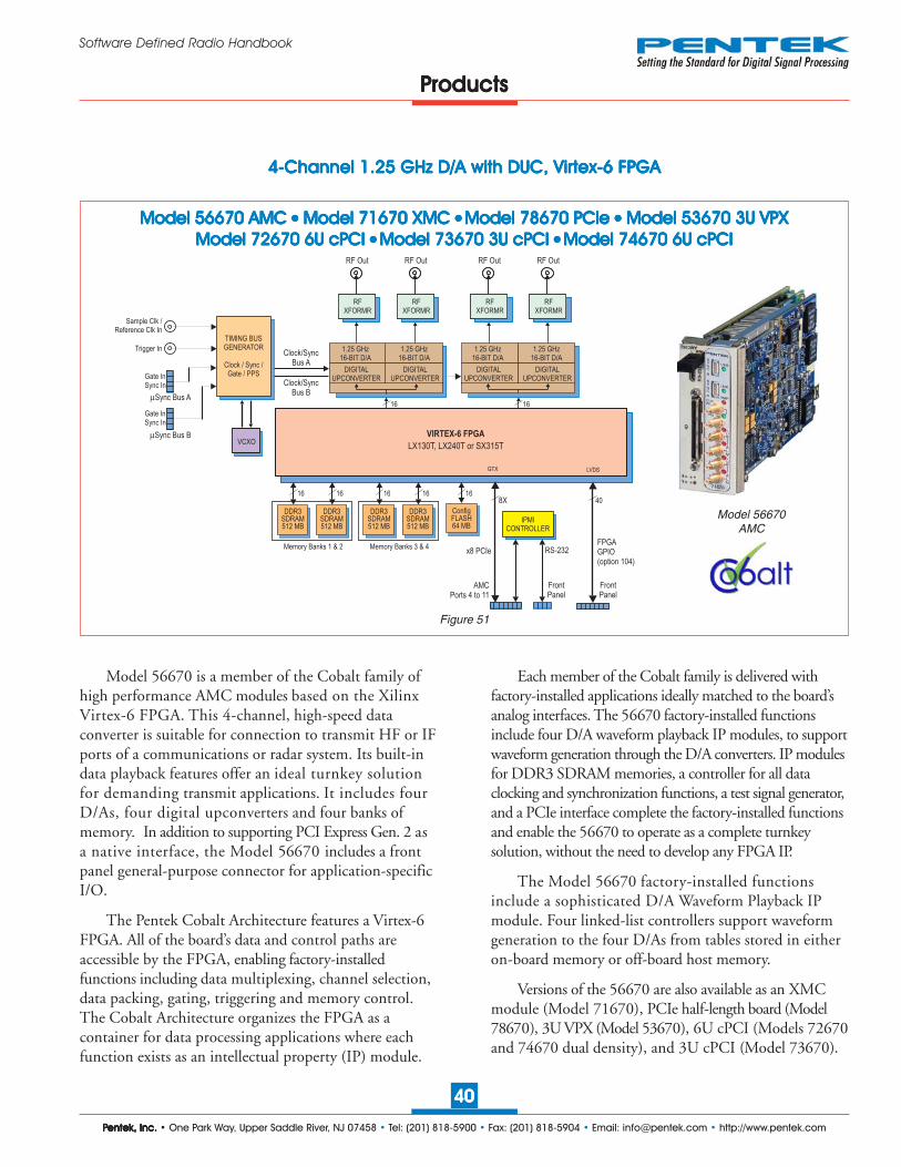
PPPPPentek, Inc.entek, Inc.entek, Inc.entek, Inc.entek, Inc. • One Park Way, Upper Saddle River, NJ 07458 • Tel: (201) 818-5900 • Fax: (201) 818-5904 • Email: [email protected] • http://www.pentek.com
4040404040
Software Defined Radio Handbook
Figure 51
4-4-4-4-4-Channel 1.25 GHz D/A with DUC, VirChannel 1.25 GHz D/A with DUC, VirChannel 1.25 GHz D/A with DUC, VirChannel 1.25 GHz D/A with DUC, VirChannel 1.25 GHz D/A with DUC, Virtex-6 FPGAtex-6 FPGAtex-6 FPGAtex-6 FPGAtex-6 FPGA
Model 56670 AMC Model 56670 AMC Model 56670 AMC Model 56670 AMC Model 56670 AMC ●●●●● Model 71670 XMC Model 71670 XMC Model 71670 XMC Model 71670 XMC Model 71670 XMC ● ● ● ● ● Model 78670 PCIe Model 78670 PCIe Model 78670 PCIe Model 78670 PCIe Model 78670 PCIe ●●●●● Model 53670 3U VPX Model 53670 3U VPX Model 53670 3U VPX Model 53670 3U VPX Model 53670 3U VPXModel 72670 6U cPCI Model 72670 6U cPCI Model 72670 6U cPCI Model 72670 6U cPCI Model 72670 6U cPCI ● ● ● ● ● Model 73670 3U cPCI Model 73670 3U cPCI Model 73670 3U cPCI Model 73670 3U cPCI Model 73670 3U cPCI ● ● ● ● ● Model 74670 6U cPCIModel 74670 6U cPCIModel 74670 6U cPCIModel 74670 6U cPCIModel 74670 6U cPCI
TIMING BUSGENERATOR
Clock / Sync /Gate / PPS
VCXO
16
Sample Clk /Reference Clk In
16
ConfigFLASH64 MB
16
DDR3SDRAM512 MB
DDR3SDRAM512 MB
1616
DDR3SDRAM512 MB
DDR3SDRAM512 MB
Memory Banks 1 & 2 Memory Banks 3 & 4
Clock/SyncBus A
40
LVDS
FPGAGPIO(option 104)
RFXFORMR
16-BIT D/A1.25 GHz
DIGITALUPCONVERTER
RF Out
RFXFORMR
RFXFORMR
1.25 GHz16-BIT D/A
DIGITALUPCONVERTER
RF Out
RFXFORMR
RFXFORMR
16-BIT D/A1.25 GHz
DIGITALUPCONVERTER
RF Out
RFXFORMR
RFXFORMR
1.25 GHz16-BIT D/A
DIGITALUPCONVERTER
RF Out
RFXFORMR
16 16
Gate InSync In
μSync Bus A
Gate InSync In
μSync Bus B
Trigger In
Clock/SyncBus B
VIRTEX-6 FPGA
LX130T, LX240T or SX315T
GTX
x8 PCIe
8X
FrontPanel
FrontPanel
AMCPorts 4 to 11
IPMICONTROLLER
RS-232
Model 56670AMC
Model 56670 is a member of the Cobalt family ofhigh performance AMC modules based on the XilinxVirtex-6 FPGA. This 4-channel, high-speed dataconverter is suitable for connection to transmit HF or IFports of a communications or radar system. Its built-indata playback features offer an ideal turnkey solutionfor demanding transmit applications. It includes fourD/As, four digital upconverters and four banks ofmemory. In addition to supporting PCI Express Gen. 2 asa native interface, the Model 56670 includes a frontpanel general-purpose connector for application-specificI/O.
The Pentek Cobalt Architecture features a Virtex-6FPGA. All of the board’s data and control paths areaccessible by the FPGA, enabling factory-installedfunctions including data multiplexing, channel selection,data packing, gating, triggering and memory control.The Cobalt Architecture organizes the FPGA as acontainer for data processing applications where eachfunction exists as an intellectual property (IP) module.
Each member of the Cobalt family is delivered withfactory-installed applications ideally matched to the board’sanalog interfaces. The 56670 factory-installed functionsinclude four D/A waveform playback IP modules, to supportwaveform generation through the D/A converters. IP modulesfor DDR3 SDRAM memories, a controller for all dataclocking and synchronization functions, a test signal generator,and a PCIe interface complete the factory-installed functionsand enable the 56670 to operate as a complete turnkeysolution, without the need to develop any FPGA IP.
The Model 56670 factory-installed functionsinclude a sophisticated D/A Waveform Playback IPmodule. Four linked-list controllers support waveformgeneration to the four D/As from tables stored in eitheron-board memory or off-board host memory.
Versions of the 56670 are also available as an XMCmodule (Model 71670), PCIe half-length board (Model78670), 3U VPX (Model 53670), 6U cPCI (Models 72670and 74670 dual density), and 3U cPCI (Model 73670).
PPPPProductsroductsroductsroductsroducts

PPPPPentek, Inc.entek, Inc.entek, Inc.entek, Inc.entek, Inc. • One Park Way, Upper Saddle River, NJ 07458 • Tel: (201) 818-5900 • Fax: (201) 818-5904 • Email: [email protected] • http://www.pentek.com
4141414141
Software Defined Radio Handbook
Figure 52
PPPPProductsroductsroductsroductsroducts
4-4-4-4-4-Channel 1.25 GHz D/A with DUC, Extended InterpolationChannel 1.25 GHz D/A with DUC, Extended InterpolationChannel 1.25 GHz D/A with DUC, Extended InterpolationChannel 1.25 GHz D/A with DUC, Extended InterpolationChannel 1.25 GHz D/A with DUC, Extended Interpolation, Vir, Vir, Vir, Vir, Virtex-6 FPGAtex-6 FPGAtex-6 FPGAtex-6 FPGAtex-6 FPGA
Model 71671 XMC Model 71671 XMC Model 71671 XMC Model 71671 XMC Model 71671 XMC ● ● ● ● ● Model 78671 PCIe Model 78671 PCIe Model 78671 PCIe Model 78671 PCIe Model 78671 PCIe ●●●●● Model 53671 3U VPX Model 53671 3U VPX Model 53671 3U VPX Model 53671 3U VPX Model 53671 3U VPX ●●●●● Model 56671 AMC Model 56671 AMC Model 56671 AMC Model 56671 AMC Model 56671 AMCModel 72671 6U cPCI Model 72671 6U cPCI Model 72671 6U cPCI Model 72671 6U cPCI Model 72671 6U cPCI ● ● ● ● ● Model 73671 3U cPCI Model 73671 3U cPCI Model 73671 3U cPCI Model 73671 3U cPCI Model 73671 3U cPCI ● ● ● ● ● Model 74671 6U cPCIModel 74671 6U cPCIModel 74671 6U cPCIModel 74671 6U cPCIModel 74671 6U cPCI
D/AWAVEFORMPLAYBACK
IP MODULE 1
toD/A Ch 1 & 2
GigabitSerial I/OPCIe
FPGAGPIO
(supports user installed IP)
MemoryBank 1
MemoryBank 2
MemoryBank 3
MemoryBank 4
VIRTEX-6 FPGA DATAFLOW DETAILVIRTEX-6 FPGA DATAFLOW DETAIL
DATAUNPACKING
& FLOWCONTROL
MUX
LINKED-LISTDMA ENGINE
toMem
Bank 1
MEMORYCONTROL
8X 4X 4X 40
D/AWAVEFORMPLAYBACK
IP MODULE 2
DATAUNPACKING
& FLOWCONTROL
MUX
LINKED-LISTDMA ENGINE
toMem
Bank 2
MEMORYCONTROL
D/AWAVEFORMPLAYBACK
IP MODULE 3
DATAUNPACKING
& FLOWCONTROL
MUX
LINKED-LISTDMA ENGINE
toMem
Bank 3
MEMORYCONTROL
D/AWAVEFORMPLAYBACK
IP MODULE 4
DATAUNPACKING
& FLOWCONTROL
MUX
LINKED-LISTDMA ENGINE
toMem
Bank 4
MEMORYCONTROL
TESTSIGNAL
GENERATOR
PCIe INTERFACE
DATAINTERLEAVER
16toD/A Ch 3 & 4
DATAINTERLEAVER
16
INTERPOLATOR2 TO 65536
IP CORE
INTERPOLATOR2 TO 65536
IP CORE
INTERPOLATOR2 TO 65536
IP CORE
INTERPOLATOR2 TO 65536
IP CORE
Model 71671XMC
Model 71671 is a member of the Cobalt family of highperformance XMC modules based on the Xilinx Virtex-6FPGA. A multichannel, high-speed data converter based onthe Model 71670 described in the previous page, it includesfactory-installed IP cores to enhance the performance of the71670 and address the requirements of many applications.
The Model 56671 factory-installed functionsinclude a sophisticated D/A Waveform Playback IPmodule. Four linked-list controllers support waveformgeneration to the four D/As from tables stored in eitheron-board memory or off-board host memory.
Two Texas Instruments DAC3484s provide four DUC(digital upconverter) and D/A channels. Each channelaccepts a baseband real or complex data stream from theFPGA and provides that input to the upconvert, interpo-late and D/A stage.
When operating as a DUC, it interpolates and trans-lates real or complex baseband input signals to a user
selectable IF center frequency. It delivers real or quadra-ture (I+Q) analog outputs to a 16-bit D/A converter.
If translation is disabled, each D/A acts as aninterpolating 16-bit D/A with output sampling rates upto 1.25 GHz. In both modes, the D/A provides interpolationfactors of 2x, 4x, 8x and 16x.
In addition to the DAC3484, the 71671 features anFPGA-based interpolation engine which adds twoadditonal interpolation stages programmable from 2x to256x. The combined interpolation results in a rangefrom 2x to 1,048,576x for each D/A channel and is idealfor matching the digital downconversion and datareduction used on the receiving channels of manycommunications systems.
Versions of the 71671 are also available as a PCIe half-length board (Model 78671), 3U VPX (Model 53671),AMC (Model 56671), 6U cPCI (Models 72671 and74671 with dual density), and 3U cPCI (Model 73671).

PPPPPentek, Inc.entek, Inc.entek, Inc.entek, Inc.entek, Inc. • One Park Way, Upper Saddle River, NJ 07458 • Tel: (201) 818-5900 • Fax: (201) 818-5904 • Email: [email protected] • http://www.pentek.com
4242424242
Software Defined Radio Handbook
LLLLL-Band RF T-Band RF T-Band RF T-Band RF T-Band RF Tuner with 2-uner with 2-uner with 2-uner with 2-uner with 2-Channel 200 MHz A/D and VirChannel 200 MHz A/D and VirChannel 200 MHz A/D and VirChannel 200 MHz A/D and VirChannel 200 MHz A/D and Virtex-6 FPGAtex-6 FPGAtex-6 FPGAtex-6 FPGAtex-6 FPGA
Model 53690 3U VPX Model 53690 3U VPX Model 53690 3U VPX Model 53690 3U VPX Model 53690 3U VPX ●●●●● Model 71690 XMC Model 71690 XMC Model 71690 XMC Model 71690 XMC Model 71690 XMC ●●●●● Model 78690 PCIe Model 78690 PCIe Model 78690 PCIe Model 78690 PCIe Model 78690 PCIe ●●●●● Model 56690 AMC Model 56690 AMC Model 56690 AMC Model 56690 AMC Model 56690 AMCModel 72690 6U cPCI Model 72690 6U cPCI Model 72690 6U cPCI Model 72690 6U cPCI Model 72690 6U cPCI ● ● ● ● ● Model 73690 3U cPCI Model 73690 3U cPCI Model 73690 3U cPCI Model 73690 3U cPCI Model 73690 3U cPCI ● ● ● ● ● Model 74690 6U cPCIModel 74690 6U cPCIModel 74690 6U cPCIModel 74690 6U cPCIModel 74690 6U cPCI
Figure 53
PPPPProductsroductsroductsroductsroducts
Model 53690 3U VPXCOTS and rugged
VCXO
16
QDRII+SRAM8 MB
TTL Gate / TrigTTL Sync / PPS
Sample ClkRef In
Gate AGate B
Sync / PPS A
Sync / PPS B
Timing Bus
Sample Clk /Reference Clk In
A/D Clock/Sync
16 16
ConfigFLASH64 MB
16
QDRII+SRAM8 MB
16
DDR3SDRAM512 MB
DDR3SDRAM512 MB
QDRII+ option 150
16
QDRII+SRAM8 MB
1616
QDRII+SRAM8 MB
16
DDR3SDRAM512 MB
DDR3SDRAM512 MB
Memory Banks 1 & 2 Memory Banks 3 & 4
DDR3 option 155
QDRII+ option 160
DDR3 option 165
Trigger 1
200 MHz16-BIT A/D
200 MHz16-BIT A/D
1616
MAX2112
I Q
RefIn
RFIn
RefOut
12-BITD/A
2
I C2
GC
Control
Trigger 2
TIMINGGENERATOR
Clock / Sync /Gate / PPS
Ref
40
FPGAI/O
Option -104
VPX BACKPLANE
VPX-P2
GTXGTXGTXLVDS
Gigabit Serial I/O
4XGbitSerial
4XGbitSerial
4XGbitSerial
4XGbitSerial
CROSSBARSWITCH
VPX-P1
4X8X 4X
x8PCIe
Option -105
VIRTEX-6 FPGA
LX130T, LX240T or SX315T
Model 53690 is a member of the Cobalt family ofhigh performance 3U VPX boards based on the XilinxVirtex-6 FPGA. A 2-Channel high-speed data converter,it is suitable for connection directly to the RF port of acommunications or radar system. Its built-in data capturefeatures offer an ideal turnkey solution. The Model 53690includes an L-Band RF tuner, two 200 MHz, 16-bitA/Ds and four banks of memory. It features built-insupport for PCI Express over the 3U VPX backplane.
The Pentek Cobalt architecture features a Virtex-6FPGA. All of the board’s data and control paths are acces-sible by the FPGA, enabling factory-installed functionsincluding data multiplexing, channel selection, data packing,gating, triggering and memory control. The Cobalt architec-ture organizes the FPGA as a container for data processingapplications where each function exists as an intellec-tual property (IP) module.
Each member of the Cobalt family is delivered withfactory-installed applications ideally matched to the
board’s analog interfaces. The 53690 factory-installedfunctions include two A/D acquisition IP modules. IPmodules for either DDR3 or QDRII+ memories, acontroller for all data clocking and synchronizationfunctions, a test signal generator, and a PCIe interfacecomplete the factory-installed functions.
A front panel connector accepts L-Band signalsbetween 925 MHz and 2175 MHz from an antennaLNB. A Maxim MAX2112 tuner directly convertsthese signals to baseband using a broadband I/Qdownconverter. The device includes an RF variable-gain LNA (low-noise amplifier), a PLL synthesizedlocal oscillator, quadrature (I + Q) downconvertingmixers, baseband lowpass filters and variable-gainbaseband amplifiers.
Versions of the 53690 are also available as an XMCmodule (Model 71690), as a PCIe half-length board (Model78690), AMC (Model56690), 6U cPCI (Models 72690and 74690 with dual density), and 3U cPCI (Model 73690).
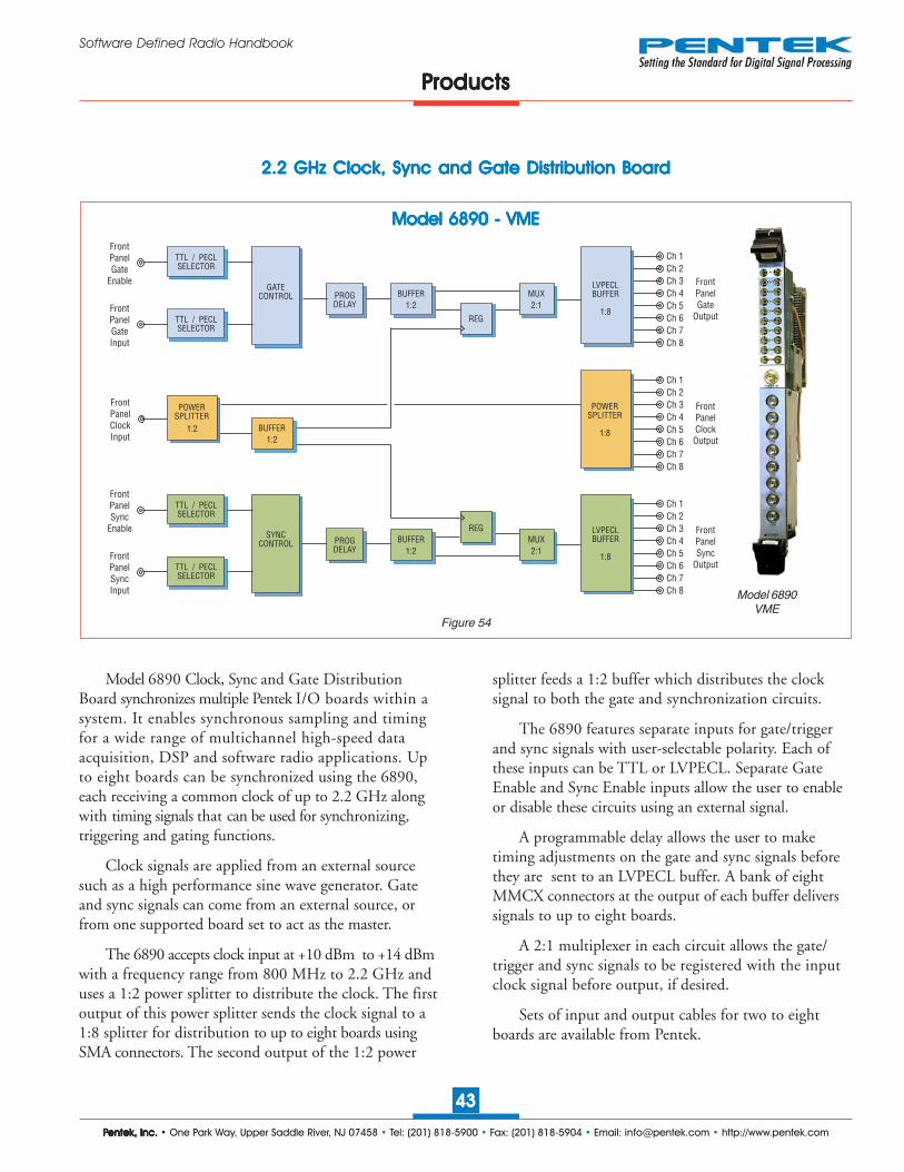
PPPPPentek, Inc.entek, Inc.entek, Inc.entek, Inc.entek, Inc. • One Park Way, Upper Saddle River, NJ 07458 • Tel: (201) 818-5900 • Fax: (201) 818-5904 • Email: [email protected] • http://www.pentek.com
4343434343
Software Defined Radio Handbook
PPPPProductsroductsroductsroductsroducts
Figure 54
Model 6890 - VMEModel 6890 - VMEModel 6890 - VMEModel 6890 - VMEModel 6890 - VME
2.2 GHz Clock, Sync and Gate Distribution Board2.2 GHz Clock, Sync and Gate Distribution Board2.2 GHz Clock, Sync and Gate Distribution Board2.2 GHz Clock, Sync and Gate Distribution Board2.2 GHz Clock, Sync and Gate Distribution Board
BUFFER1:2
BUFFER1:2
BUFFER1:2
PROGDELAY
PROGDELAY
MUX2:1
MUX2:1
FrontPanelSync
Output
FrontPanelClock
Output
FrontPanelGate
Output
Ch 1
Ch 1
Ch 1
Ch 2
Ch 2
Ch 2
Ch 3
Ch 3
Ch 3
Ch 4
Ch 4
Ch 4
Ch 5
Ch 5
Ch 5
Ch 6
Ch 6
Ch 6
Ch 7
Ch 7
Ch 7
Ch 8
Ch 8
Ch 8
LVPECLBUFFER
1:8
LVPECLBUFFER
1:8
POWERSPLITTER
1:8
POWERSPLITTER
1:2
TTL / PECLSELECTOR
TTL / PECLSELECTOR
TTL / PECLSELECTOR
TTL / PECLSELECTOR
GATECONTROL
SYNCCONTROL
FrontPanelClockInput
FrontPanelGateInput
FrontPanelSyncInput
FrontPanelGate
Enable
FrontPanelSync
Enable REG
REG
Model 6890VME
Model 6890 Clock, Sync and Gate DistributionBoard synchronizes multiple Pentek I/O boards within asystem. It enables synchronous sampling and timingfor a wide range of multichannel high-speed dataacquisition, DSP and software radio applications. Upto eight boards can be synchronized using the 6890,each receiving a common clock of up to 2.2 GHz alongwith timing signals that can be used for synchronizing,triggering and gating functions.
Clock signals are applied from an external sourcesuch as a high performance sine wave generator. Gateand sync signals can come from an external source, orfrom one supported board set to act as the master.
The 6890 accepts clock input at +10 dBm to +14 dBmwith a frequency range from 800 MHz to 2.2 GHz anduses a 1:2 power splitter to distribute the clock. The firstoutput of this power splitter sends the clock signal to a1:8 splitter for distribution to up to eight boards usingSMA connectors. The second output of the 1:2 power
splitter feeds a 1:2 buffer which distributes the clocksignal to both the gate and synchronization circuits.
The 6890 features separate inputs for gate/triggerand sync signals with user-selectable polarity. Each ofthese inputs can be TTL or LVPECL. Separate GateEnable and Sync Enable inputs allow the user to enableor disable these circuits using an external signal.
A programmable delay allows the user to maketiming adjustments on the gate and sync signals beforethey are sent to an LVPECL buffer. A bank of eightMMCX connectors at the output of each buffer deliverssignals to up to eight boards.
A 2:1 multiplexer in each circuit allows the gate/trigger and sync signals to be registered with the inputclock signal before output, if desired.
Sets of input and output cables for two to eightboards are available from Pentek.
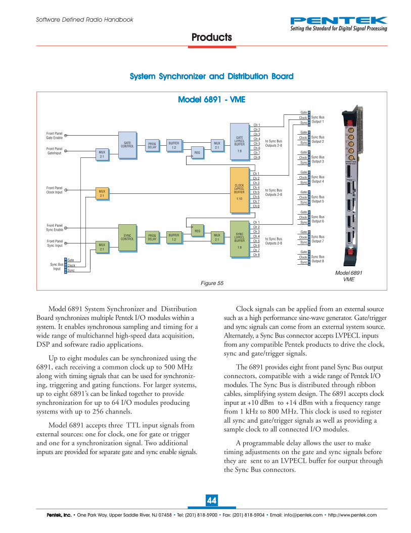
PPPPPentek, Inc.entek, Inc.entek, Inc.entek, Inc.entek, Inc. • One Park Way, Upper Saddle River, NJ 07458 • Tel: (201) 818-5900 • Fax: (201) 818-5904 • Email: [email protected] • http://www.pentek.com
4444444444
Software Defined Radio Handbook
PPPPProductsroductsroductsroductsroducts
Figure 55
System Synchronizer and Distribution BoardSystem Synchronizer and Distribution BoardSystem Synchronizer and Distribution BoardSystem Synchronizer and Distribution BoardSystem Synchronizer and Distribution Board
Model 6891 - VMEModel 6891 - VMEModel 6891 - VMEModel 6891 - VMEModel 6891 - VME
BUFFER1:2
BUFFER1:2
PROGDELAY
PROGDELAY
MUX2:1
MUX2:1
Ch 1
Ch 1
Ch 1
Ch 2
Ch 2
Ch 2
Ch 3
Ch 3
Ch 3
Ch 4
Ch 4
Ch 4
Ch 5
Ch 5
Ch 5
Ch 6
Ch 6
Ch 6
Ch 7
Ch 7
Ch 7
Ch 8
Ch 8
Ch 8
SYNCLVPECLBUFFER
1:8
GATELVPECLBUFFER
1:8
CLOCKLVPECLBUFFER
1:10
GATECONTROL
Front PanelClock Input
Front PanelGateInput
Front PanelSync Input
Front PanelGate Enable
Front PanelSync Enable REG
REG
Gate
SyncClockSync Bus
Input
MUX2:1
MUX2:1
MUX2:1
SYNCCONTROL
Gate
SyncClock Sync Bus
Output 8
Gate
SyncClock Sync Bus
Output 7
Gate
SyncClock Sync Bus
Output 6
Gate
SyncClock Sync Bus
Output 5
Gate
SyncClock Sync Bus
Output 4
Gate
SyncClock Sync Bus
Output 3
Gate
SyncClock Sync Bus
Output 2
Gate
SyncClock Sync Bus
Output 1
to Sync BusOutputs 2-8
to Sync BusOutputs 2-8
to Sync BusOutputs 2-8
Model 6891VME
Model 6891 System Synchronizer and DistributionBoard synchronizes multiple Pentek I/O modules within asystem. It enables synchronous sampling and timing for awide range of multichannel high-speed data acquisition,DSP and software radio applications.
Up to eight modules can be synchronized using the6891, each receiving a common clock up to 500 MHzalong with timing signals that can be used for synchroniz-ing, triggering and gating functions. For larger systems,up to eight 6891’s can be linked together to providesynchronization for up to 64 I/O modules producingsystems with up to 256 channels.
Model 6891 accepts three TTL input signals fromexternal sources: one for clock, one for gate or triggerand one for a synchronization signal. Two additionalinputs are provided for separate gate and sync enable signals.
Clock signals can be applied from an external sourcesuch as a high performance sine-wave generator. Gate/triggerand sync signals can come from an external system source.Alternately, a Sync Bus connector accepts LVPECL inputsfrom any compatible Pentek products to drive the clock,sync and gate/trigger signals.
The 6891 provides eight front panel Sync Bus outputconnectors, compatible with a wide range of Pentek I/Omodules. The Sync Bus is distributed through ribboncables, simplifying system design. The 6891 accepts clockinput at +10 dBm to +14 dBm with a frequency rangefrom 1 kHz to 800 MHz. This clock is used to registerall sync and gate/trigger signals as well as providing asample clock to all connected I/O modules.
A programmable delay allows the user to maketiming adjustments on the gate and sync signals beforethey are sent to an LVPECL buffer for output throughthe Sync Bus connectors.
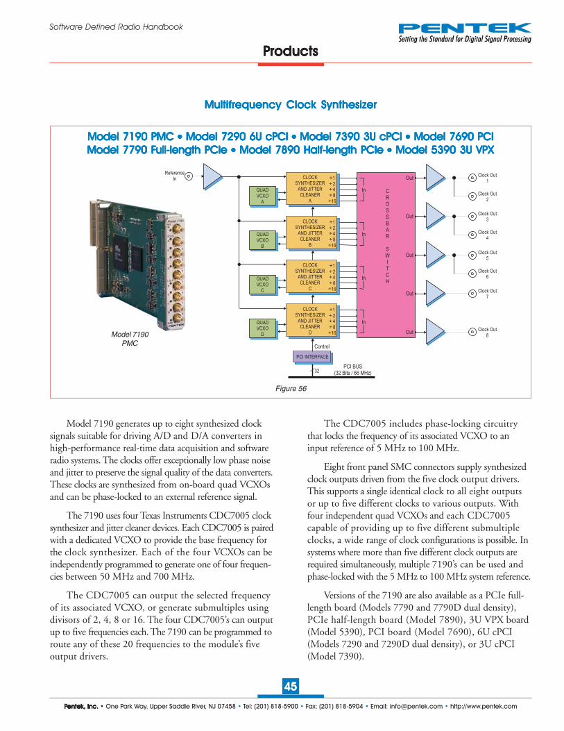
PPPPPentek, Inc.entek, Inc.entek, Inc.entek, Inc.entek, Inc. • One Park Way, Upper Saddle River, NJ 07458 • Tel: (201) 818-5900 • Fax: (201) 818-5904 • Email: [email protected] • http://www.pentek.com
4545454545
Software Defined Radio Handbook
ReferenceIn
Control
PCI INTERFACE
PCI BUS(32 Bits / 66 MHz)32
Clock Out1
Clock Out2
Clock Out3
Clock Out4
Clock Out5
Clock Out6
Clock Out7
Clock Out8
CLOCKSYNTHESIZER
AND JITTERCLEANER
A
1÷÷ 2÷ 4÷ 8÷16
QUADVCXO
A
CLOCKSYNTHESIZER
AND JITTERCLEANER
B
1÷÷ 2÷ 4÷ 8÷16
CLOCKSYNTHESIZER
AND JITTERCLEANER
C
1÷÷ 2÷ 4÷ 8÷16
CLOCKSYNTHESIZER
AND JITTERCLEANER
D
1÷÷ 2÷ 4÷ 8÷16
Supports:any In to any Out,any In to multiple
Outs
CROSSBAR
SWITCH
In
In
In
In
Out
Out
Out
Out
Out
QUADVCXO
B
QUADVCXO
C
QUADVCXO
D
PPPPProductsroductsroductsroductsroducts
Figure 56
Multifrequency Clock SynthesizerMultifrequency Clock SynthesizerMultifrequency Clock SynthesizerMultifrequency Clock SynthesizerMultifrequency Clock Synthesizer
Model 7190PMC
Model 7190 generates up to eight synthesized clocksignals suitable for driving A/D and D/A converters inhigh-performance real-time data acquisition and softwareradio systems. The clocks offer exceptionally low phase noiseand jitter to preserve the signal quality of the data converters.These clocks are synthesized from on-board quad VCXOsand can be phase-locked to an external reference signal.
The 7190 uses four Texas Instruments CDC7005 clocksynthesizer and jitter cleaner devices. Each CDC7005 is pairedwith a dedicated VCXO to provide the base frequency forthe clock synthesizer. Each of the four VCXOs can beindependently programmed to generate one of four frequen-cies between 50 MHz and 700 MHz.
The CDC7005 can output the selected frequencyof its associated VCXO, or generate submultiples usingdivisors of 2, 4, 8 or 16. The four CDC7005’s can outputup to five frequencies each. The 7190 can be programmed toroute any of these 20 frequencies to the module’s fiveoutput drivers.
The CDC7005 includes phase-locking circuitrythat locks the frequency of its associated VCXO to aninput reference of 5 MHz to 100 MHz.
Eight front panel SMC connectors supply synthesizedclock outputs driven from the five clock output drivers.This supports a single identical clock to all eight outputsor up to five different clocks to various outputs. Withfour independent quad VCXOs and each CDC7005capable of providing up to five different submultipleclocks, a wide range of clock configurations is possible. Insystems where more than five different clock outputs arerequired simultaneously, multiple 7190’s can be used andphase-locked with the 5 MHz to 100 MHz system reference.
Versions of the 7190 are also available as a PCIe full-length board (Models 7790 and 7790D dual density),PCIe half-length board (Model 7890), 3U VPX board(Model 5390), PCI board (Model 7690), 6U cPCI(Models 7290 and 7290D dual density), or 3U cPCI(Model 7390).
Model 7190 PMC Model 7190 PMC Model 7190 PMC Model 7190 PMC Model 7190 PMC ●●●●● Model 7290 6U cPCI Model 7290 6U cPCI Model 7290 6U cPCI Model 7290 6U cPCI Model 7290 6U cPCI ●●●●● Model 7390 3U cPCI Model 7390 3U cPCI Model 7390 3U cPCI Model 7390 3U cPCI Model 7390 3U cPCI ●●●●● Model 7690 PCI Model 7690 PCI Model 7690 PCI Model 7690 PCI Model 7690 PCIModel 7790 FModel 7790 FModel 7790 FModel 7790 FModel 7790 Full-length PCIe ull-length PCIe ull-length PCIe ull-length PCIe ull-length PCIe ●●●●● Model 7890 Half-length PCIe Model 7890 Half-length PCIe Model 7890 Half-length PCIe Model 7890 Half-length PCIe Model 7890 Half-length PCIe ●●●●● Model 5390 3U VPX Model 5390 3U VPX Model 5390 3U VPX Model 5390 3U VPX Model 5390 3U VPX
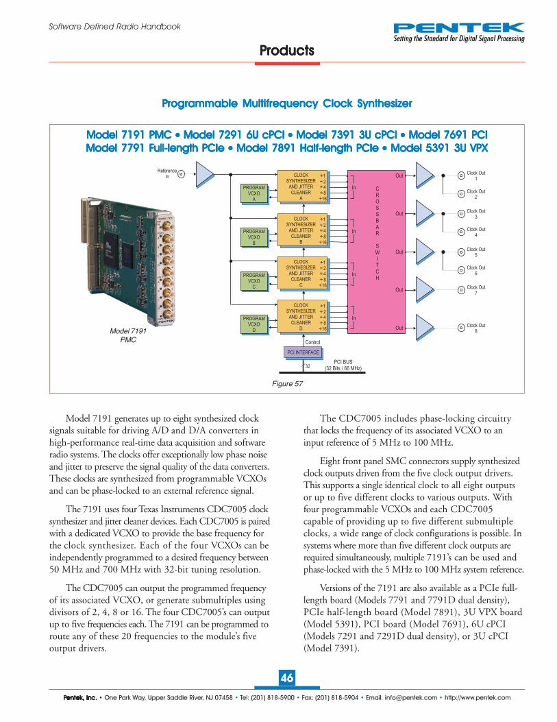
PPPPPentek, Inc.entek, Inc.entek, Inc.entek, Inc.entek, Inc. • One Park Way, Upper Saddle River, NJ 07458 • Tel: (201) 818-5900 • Fax: (201) 818-5904 • Email: [email protected] • http://www.pentek.com
4646464646
Software Defined Radio Handbook
ReferenceIn
Control
PCI INTERFACE
PCI BUS(32 Bits / 66 MHz)32
Clock Out1
Clock Out2
Clock Out3
Clock Out4
Clock Out5
Clock Out6
Clock Out7
Clock Out8
CLOCKSYNTHESIZER
AND JITTERCLEANER
A
1÷÷ 2÷ 4÷ 8÷16
PROGRAMVCXO
A
CLOCKSYNTHESIZER
AND JITTERCLEANER
B
1÷÷ 2÷ 4÷ 8÷16
CLOCKSYNTHESIZER
AND JITTERCLEANER
C
1÷÷ 2÷ 4÷ 8÷16
CLOCKSYNTHESIZER
AND JITTERCLEANER
D
1÷÷ 2÷ 4÷ 8÷16
Supports:any In to any Out,any In to multiple
Outs
CROSSBAR
SWITCH
In
In
In
In
Out
Out
Out
Out
Out
PROGRAMVCXO
B
PROGRAMVCXO
C
PROGRAMVCXO
D
PPPPProductsroductsroductsroductsroducts
Figure 57
Model 7191 PMC Model 7191 PMC Model 7191 PMC Model 7191 PMC Model 7191 PMC ●●●●● Model 7291 6U cPCI Model 7291 6U cPCI Model 7291 6U cPCI Model 7291 6U cPCI Model 7291 6U cPCI ●●●●● Model 7391 3U cPCI Model 7391 3U cPCI Model 7391 3U cPCI Model 7391 3U cPCI Model 7391 3U cPCI ●●●●● Model 7691 PCI Model 7691 PCI Model 7691 PCI Model 7691 PCI Model 7691 PCIModel 7791 FModel 7791 FModel 7791 FModel 7791 FModel 7791 Full-length PCIe ull-length PCIe ull-length PCIe ull-length PCIe ull-length PCIe ●●●●● Model 7891 Half-length PCIe Model 7891 Half-length PCIe Model 7891 Half-length PCIe Model 7891 Half-length PCIe Model 7891 Half-length PCIe ●●●●● Model 5391 3U VPX Model 5391 3U VPX Model 5391 3U VPX Model 5391 3U VPX Model 5391 3U VPX
Model 7191 generates up to eight synthesized clocksignals suitable for driving A/D and D/A converters inhigh-performance real-time data acquisition and softwareradio systems. The clocks offer exceptionally low phase noiseand jitter to preserve the signal quality of the data converters.These clocks are synthesized from programmable VCXOsand can be phase-locked to an external reference signal.
The 7191 uses four Texas Instruments CDC7005 clocksynthesizer and jitter cleaner devices. Each CDC7005 is pairedwith a dedicated VCXO to provide the base frequency forthe clock synthesizer. Each of the four VCXOs can beindependently programmed to a desired frequency between50 MHz and 700 MHz with 32-bit tuning resolution.
The CDC7005 can output the programmed frequencyof its associated VCXO, or generate submultiples usingdivisors of 2, 4, 8 or 16. The four CDC7005’s can outputup to five frequencies each. The 7191 can be programmed toroute any of these 20 frequencies to the module’s fiveoutput drivers.
The CDC7005 includes phase-locking circuitrythat locks the frequency of its associated VCXO to aninput reference of 5 MHz to 100 MHz.
Eight front panel SMC connectors supply synthesizedclock outputs driven from the five clock output drivers.This supports a single identical clock to all eight outputsor up to five different clocks to various outputs. Withfour programmable VCXOs and each CDC7005capable of providing up to five different submultipleclocks, a wide range of clock configurations is possible. Insystems where more than five different clock outputs arerequired simultaneously, multiple 7191’s can be used andphase-locked with the 5 MHz to 100 MHz system reference.
Versions of the 7191 are also available as a PCIe full-length board (Models 7791 and 7791D dual density),PCIe half-length board (Model 7891), 3U VPX board(Model 5391), PCI board (Model 7691), 6U cPCI(Models 7291 and 7291D dual density), or 3U cPCI(Model 7391).
Model 7191PMC
PPPPProgrammable Multifrequency Clock Synthesizerrogrammable Multifrequency Clock Synthesizerrogrammable Multifrequency Clock Synthesizerrogrammable Multifrequency Clock Synthesizerrogrammable Multifrequency Clock Synthesizer
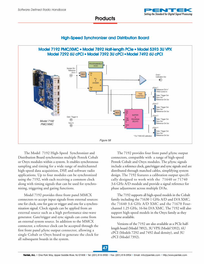
PPPPPentek, Inc.entek, Inc.entek, Inc.entek, Inc.entek, Inc. • One Park Way, Upper Saddle River, NJ 07458 • Tel: (201) 818-5900 • Fax: (201) 818-5904 • Email: [email protected] • http://www.pentek.com
4747474747
Software Defined Radio Handbook
Figure 58
Model 7192 PMC/XMC Model 7192 PMC/XMC Model 7192 PMC/XMC Model 7192 PMC/XMC Model 7192 PMC/XMC ●●●●● Model 7892 Half-length PCIe Model 7892 Half-length PCIe Model 7892 Half-length PCIe Model 7892 Half-length PCIe Model 7892 Half-length PCIe ●●●●● Model 5393 3U VPX Model 5393 3U VPX Model 5393 3U VPX Model 5393 3U VPX Model 5393 3U VPXModel 7292 6U cPCI Model 7292 6U cPCI Model 7292 6U cPCI Model 7292 6U cPCI Model 7292 6U cPCI ●●●●● Model 7392 3U cPCI Model 7392 3U cPCI Model 7392 3U cPCI Model 7392 3U cPCI Model 7392 3U cPCI ● ● ● ● ● Model 7492 6U cPCIModel 7492 6U cPCIModel 7492 6U cPCIModel 7492 6U cPCIModel 7492 6U cPCI
High-Speed Synchronizer and Distribution BoardHigh-Speed Synchronizer and Distribution BoardHigh-Speed Synchronizer and Distribution BoardHigh-Speed Synchronizer and Distribution BoardHigh-Speed Synchronizer and Distribution Board
Model 7192PMC/XMC
PLL&
DIVIDER
Gate / Trigger Out
Sample Clk /Reference
Clk InMUX
ClkIn
RefIn
:N
PROGRAMMABLEVCXO
Clock /Calibration Out
:N
BUFFER&
PROGRAMDELAYS
Clk/RefIn
Sync OutReference Clk Out
TWSI Control InReference Clk In *
Gate / Trigger OutSync OutReference Clk Out
MUX
Trig/GateIn
SyncIn
TWSICONTROL
Gate / Trigger OutSync OutReference Clk Out
Gate / Trigger OutSync OutReference Clk Out
Gate / Trigger In
Sync In
�Sync 3
�Sync 2
�Sync 1
�Sync 4
* For 71640 A/D calibration
The Model 7192 High-Speed Synchronizer andDistribution Board synchronizes multiple Pentek Cobaltor Onyx modules within a system. It enables synchronoussampling and timing for a wide range of multichannelhigh-speed data acquisition, DSP, and software radioapplications. Up to four modules can be synchronizedusing the 7192, with each receiving a common clockalong with timing signals that can be used for synchro-nizing, triggering and gating functions.
Model 7192 provides three front panel MMCXconnectors to accept input signals from external sources:one for clock, one for gate or trigger and one for a synchro-nization signal. Clock signals can be applied from anexternal source such as a high performance sine-wavegenerator. Gate/trigger and sync signals can come froman external system source. In addition to the MMCXconnector, a reference clock can be accepted through thefirst front panel µSync output connector, allowing asingle Cobalt or Onyx board to generate the clock forall subsequent boards in the system.
The 7192 provides four front panel µSync outputconnectors, compatible with a range of high-speedPentek Cobalt and Onyx modules. The µSync signalsinclude a reference clock, gate/trigger and sync signals and aredistributed through matched cables, simplifying systemdesign. The 7192 features a calibration output specifi-cally designed to work with the 71640 or 717403.6 GHz A/D module and provide a signal reference forphase adjustment across multiple D/As.
The 7192 supports all high-speed models in the Cobaltfamily including the 71630 1 GHz A/D and D/A XMC,the 71640 3.6 GHz A/D XMC and the 71670 Four-channel 1.25 GHz, 16-bit D/A XMC. The 7192 will alsosupport high-speed models in the Onyx family as theybecome available.
Versions of the 7192 are also available as a PCIe half-length board (Model 7892), 3U VPX (Model 5392), 6UcPCI (Models 7292 and 7492 dual density), and 3UcPCI (Model 7392).
PPPPProductsroductsroductsroductsroducts

PPPPPentek, Inc.entek, Inc.entek, Inc.entek, Inc.entek, Inc. • One Park Way, Upper Saddle River, NJ 07458 • Tel: (201) 818-5900 • Fax: (201) 818-5904 • Email: [email protected] • http://www.pentek.com
4848484848
Software Defined Radio Handbook
Figure 59
Model 7893 - Half-length PCIeModel 7893 - Half-length PCIeModel 7893 - Half-length PCIeModel 7893 - Half-length PCIeModel 7893 - Half-length PCIe
System Synchronizer and Distribution BoardSystem Synchronizer and Distribution BoardSystem Synchronizer and Distribution BoardSystem Synchronizer and Distribution BoardSystem Synchronizer and Distribution Board
PPPPProductsroductsroductsroductsroducts
PLL&
DIVIDER
CLKIN
PROGRAMVCXO
Clock Out 1: N
BUFFER&
PROGRAMDELAYS
TTLSync / PPS B In
Timing Bus Out 2through
Timing Bus Out 7
USBINTERFACE
USB
Sample Clk A
Sample Clk BGate / Trig AGate / Trig B
Sync / PPS A
Sync / PPS B
Timing Bus In
Sample Clk ASample Clk BGate / Trig AGate / Trig BSync / PPS A
Sync / PPS B
Timing Bus Out 1
Sample Clk ASample Clk BGate / Trig AGate / Trig BSync / PPS A
Sync / PPS B
Timing Bus Out 8
MUX
TTLSync / PPS A In
MUX
MUX
MUX
TTLGate / Trig In
MUX
Sample Clk /Reference Clk In
Clock Out 2
Clock Out 3
Clock Out 4
: N
: N
: N
: N
Gate / Trig A
Gate / Trig B
Sync / PPS A
Sync / PPS B
MUX
USB Sync / PPS
USB Gate / Trig
REFCLKIN
CONTROLVOLTAGE
Sample Clk A
Sample Clk B
Sample Clk A
Sample Clk B
Control
USB Gate / Trig
USB Sync / PPS
Model 7893 System Synchronizer and DistributionBoard synchronizes multiple Pentek Cobalt and Onyxboards within a system. It enables synchronous sampling,playback and timing for a wide range of multichannelhigh-speed data acquisition, DSP and software radioapplications.
Up to eight boards can be synchronized using the7893, each receiving a common clock up to 800 MHzalong with timing signals that can be used for synchroniz-ing, triggering and gating functions. For larger systems,up to eight 7893s can be linked together to provide synchro-nization for up to 64 Cobalt or Onyx boards.
The Model 7893 provides four front panel SMAconnectors to accept LVTTL input signals fromexternal sources: two for Sync/PPS and one for Gate/Trigger. In addition to the synchronization signals, a frontpanel SMA connector accepts sample clocks up to 800 MHzor, in an alternate mode, accepts a 10 MHz referenceclock to lock an on-board VCXO sample clock source.
The 7893 provides eight timing bus output connec-tors for distributing all needed timing and clock signalsto the front panels of Cobalt and Onyx boards via ribboncables. The 7893 locks the Gate/Trigger and Sync/PPSsignals to the system’s sample clock. The 7893 alsoprovides four front panel SMA connectors for distrib-uting sample clocks to other boards in the system.
The 7893 can accept a clock from either the front panelSMA connector or from the timing bus input connector. Aprogrammable on-board VCXO clock generator can belocked to a user-supplied, 10 MHz reference.
The 7893 supports a wide range of products in theCobalt family including the 78620 and 78621 three-channelA/D 200 MHz transceivers, the 78650 and 78651 two-channelA/D 500 MHz transceivers, the 78660, 78661 and 78662four-channel 200 MHz A/Ds, and the 78690 L-Band RFTuner. The 7893 also supports the Onyx 78760 four-channel 200 MHz A/D and will support all complemen-tary models in the Onyx family as they become available.
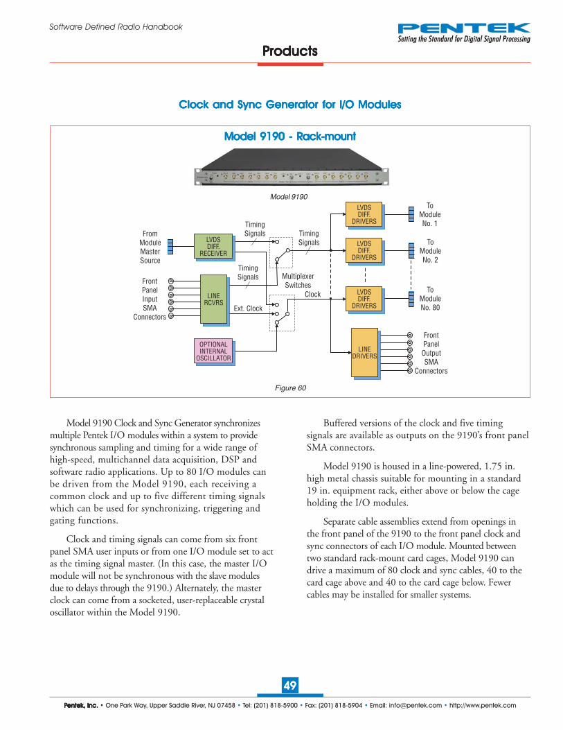
PPPPPentek, Inc.entek, Inc.entek, Inc.entek, Inc.entek, Inc. • One Park Way, Upper Saddle River, NJ 07458 • Tel: (201) 818-5900 • Fax: (201) 818-5904 • Email: [email protected] • http://www.pentek.com
4949494949
Software Defined Radio Handbook
PPPPProductsroductsroductsroductsroducts
Figure 60
Clock and Sync Generator for I/O ModulesClock and Sync Generator for I/O ModulesClock and Sync Generator for I/O ModulesClock and Sync Generator for I/O ModulesClock and Sync Generator for I/O Modules
ToModuleNo. 80
FromModuleMasterSource
ToModuleNo. 2
ToModuleNo. 1
OPTIONALINTERNAL
OSCILLATOR
LVDSDIFF.
RECEIVER
LVDSDIFF.
DRIVERS
LVDSDIFF.
DRIVERS
LVDSDIFF.
DRIVERS
FrontPanel
OutputSMA
Connectors
LINEDRIVERS
FrontPanelInputSMA
Connectors
TimingSignals
MultiplexerSwitches
TimingSignals
TimingSignals
Ext. Clock
ClockLINERCVRS
Model 9190
Model 9190 - RModel 9190 - RModel 9190 - RModel 9190 - RModel 9190 - Rack-mountack-mountack-mountack-mountack-mount
Model 9190 Clock and Sync Generator synchronizesmultiple Pentek I/O modules within a system to providesynchronous sampling and timing for a wide range ofhigh-speed, multichannel data acquisition, DSP andsoftware radio applications. Up to 80 I/O modules canbe driven from the Model 9190, each receiving acommon clock and up to five different timing signalswhich can be used for synchronizing, triggering andgating functions.
Clock and timing signals can come from six frontpanel SMA user inputs or from one I/O module set to actas the timing signal master. (In this case, the master I/Omodule will not be synchronous with the slave modulesdue to delays through the 9190.) Alternately, the masterclock can come from a socketed, user-replaceable crystaloscillator within the Model 9190.
Buffered versions of the clock and five timingsignals are available as outputs on the 9190’s front panelSMA connectors.
Model 9190 is housed in a line-powered, 1.75 in.high metal chassis suitable for mounting in a standard19 in. equipment rack, either above or below the cageholding the I/O modules.
Separate cable assemblies extend from openings inthe front panel of the 9190 to the front panel clock andsync connectors of each I/O module. Mounted betweentwo standard rack-mount card cages, Model 9190 candrive a maximum of 80 clock and sync cables, 40 to thecard cage above and 40 to the card cage below. Fewercables may be installed for smaller systems.
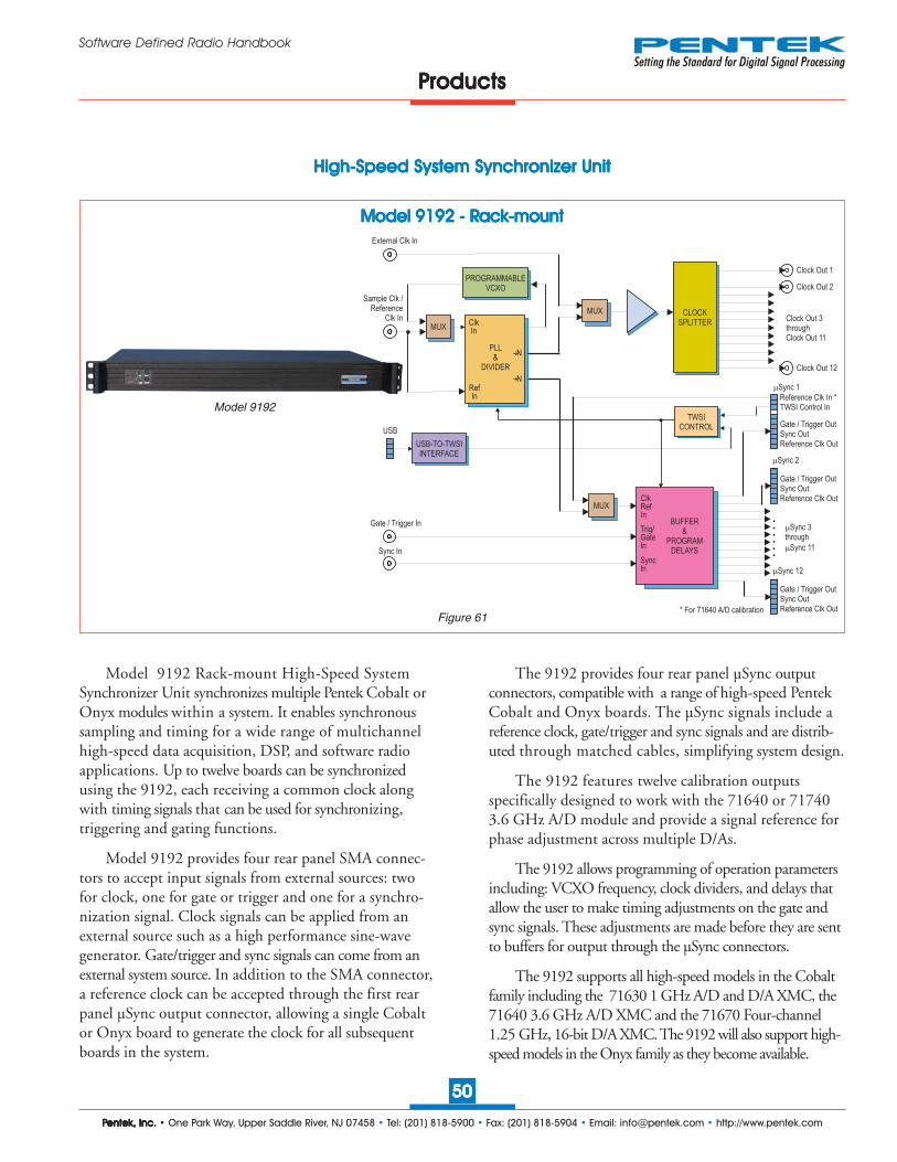
PPPPPentek, Inc.entek, Inc.entek, Inc.entek, Inc.entek, Inc. • One Park Way, Upper Saddle River, NJ 07458 • Tel: (201) 818-5900 • Fax: (201) 818-5904 • Email: [email protected] • http://www.pentek.com
5050505050
Software Defined Radio Handbook
PPPPProductsroductsroductsroductsroducts
High-Speed System Synchronizer UnitHigh-Speed System Synchronizer UnitHigh-Speed System Synchronizer UnitHigh-Speed System Synchronizer UnitHigh-Speed System Synchronizer Unit
Model 9192 - RModel 9192 - RModel 9192 - RModel 9192 - RModel 9192 - Rack-mountack-mountack-mountack-mountack-mount
PLL&
DIVIDER
Gate / Trigger Out
Sample Clk /Reference
Clk InMUX
ClkIn
RefIn
:N
PROGRAMMABLEVCXO
Clock Out 1
:N
BUFFER&
PROGRAMDELAYS
ClkRefIn
Sync OutReference Clk Out
TWSI Control InReference Clk In *
Gate / Trigger OutSync OutReference Clk Out
MUX
Trig/GateIn
SyncIn
TWSICONTROL
Gate / Trigger OutSync OutReference Clk Out
Gate / Trigger In
Sync In
�Sync 2
�Sync 1
�Sync 12
* For 71640 A/D calibration
�Sync 3through
�Sync 11
Clock Out 2
Clock Out 12
CLOCKSPLITTER
Clock Out 3throughClock Out 11
External Clk In
MUX
USB-TO-TWSIINTERFACE
USB
Model 9192
Model 9192 Rack-mount High-Speed SystemSynchronizer Unit synchronizes multiple Pentek Cobalt orOnyx modules within a system. It enables synchronoussampling and timing for a wide range of multichannelhigh-speed data acquisition, DSP, and software radioapplications. Up to twelve boards can be synchronizedusing the 9192, each receiving a common clock alongwith timing signals that can be used for synchronizing,triggering and gating functions.
Model 9192 provides four rear panel SMA connec-tors to accept input signals from external sources: twofor clock, one for gate or trigger and one for a synchro-nization signal. Clock signals can be applied from anexternal source such as a high performance sine-wavegenerator. Gate/trigger and sync signals can come from anexternal system source. In addition to the SMA connector,a reference clock can be accepted through the first rearpanel µSync output connector, allowing a single Cobaltor Onyx board to generate the clock for all subsequentboards in the system.
Figure 61
The 9192 provides four rear panel µSync outputconnectors, compatible with a range of high-speed PentekCobalt and Onyx boards. The µSync signals include areference clock, gate/trigger and sync signals and are distrib-uted through matched cables, simplifying system design.
The 9192 features twelve calibration outputsspecifically designed to work with the 71640 or 717403.6 GHz A/D module and provide a signal reference forphase adjustment across multiple D/As.
The 9192 allows programming of operation parametersincluding: VCXO frequency, clock dividers, and delays thatallow the user to make timing adjustments on the gate andsync signals. These adjustments are made before they are sentto buffers for output through the µSync connectors.
The 9192 supports all high-speed models in the Cobaltfamily including the 71630 1 GHz A/D and D/A XMC, the71640 3.6 GHz A/D XMC and the 71670 Four-channel1.25 GHz, 16-bit D/A XMC. The 9192 will also support high-speed models in the Onyx family as they become available.

PPPPPentek, Inc.entek, Inc.entek, Inc.entek, Inc.entek, Inc. • One Park Way, Upper Saddle River, NJ 07458 • Tel: (201) 818-5900 • Fax: (201) 818-5904 • Email: [email protected] • http://www.pentek.com
5151515151
Software Defined Radio Handbook
ChannelsIn
ChannelsOut
200 MHz16-bit A/D
Up to 8Channels
DIGITALDOWN-
CONVERTERDecimation:2 to 65,536
INTELPROCESSOR
SYSTEM DRIVEDDR
SDRAM
HOST PROCESSORRUNNING SYSTEMFLOW
UP TO 20 TB RAID
DATA DRIVES DATA DRIVES
DATA DRIVES DATA DRIVES
MODEL RTS 2706
USB 2.0
GigabitEthernet
PS/2Keyboard
PS/2Mouse
VideoOutput
2
6
eSATA2
GPSAntenna(Optional)
800 MHzor 1.25 GHz16-bit D/A
Up to 8Channels
DIGITALUP-
CONVERTERDecimation:2 to 65,536
PPPPProductsroductsroductsroductsroducts
Model RTS 2706 Model RTS 2706 Model RTS 2706 Model RTS 2706 Model RTS 2706
Figure 62
The Talon® RTS 2706 is a turnkey, multibandrecording and playback system for recording andreproducing high-bandwidth signals. The RTS 2706uses 16-bit, 200 MHz A/D converters and providessustained recording rates up to 2.0 GB/sec in four-channelconfiguration.
The RTS 2706 uses Pentek’s high-powered Virtex-6-basedCobalt modules, that provide flexibility in channel count,with optional digital downconversion capabilities. Optional16-bit, 800 MHz D/A converters with digital upconversionallow real-time reproduction of recorded signals.
A/D sampling rate, DDC decimation and bandwidth,D/A sampling rate and DUC interpolation are amongthe GUI-selectable system parameters, providing a fully-programmable system capable of recording and reproduc-ing a wide range of signals.
Included with this system is Pentek’s SystemFlowrecording software. Optional GPS time and positionstamping allows the user to record this critical signalinformation.
Built on a Windows® 7 Professional workstation withhigh performance Intel® CoreTM i7 processor, the RTS 2706allows the user to install post-processing and analysistools to operate on the recorded data. The instrumentrecords data to the native NTFS file system, providingimmediate access to the data.
The RTS 2706 is configured in a 4U 19" rackmoun-table chassis, with hot-swap data drives, front panel USBports and I/O connectors on the rear panel. Systems arescalable to accommodate multiple chassis to increasechannel counts and aggregate data rates. All recorderchassis are connected via Ethernet and can be controlledfrom a single GUI either locally or from a remote PC.
Model RTS 2706COTS
Model RTS 2706Rugged
Eight-Eight-Eight-Eight-Eight-Channel RF/IFChannel RF/IFChannel RF/IFChannel RF/IFChannel RF/IF, 200 MS/sec R, 200 MS/sec R, 200 MS/sec R, 200 MS/sec R, 200 MS/sec Rackmount Rackmount Rackmount Rackmount Rackmount Recorderecorderecorderecorderecorder

PPPPPentek, Inc.entek, Inc.entek, Inc.entek, Inc.entek, Inc. • One Park Way, Upper Saddle River, NJ 07458 • Tel: (201) 818-5900 • Fax: (201) 818-5904 • Email: [email protected] • http://www.pentek.com
5252525252
Software Defined Radio Handbook
PPPPProductsroductsroductsroductsroducts
Model RTS 2707 Model RTS 2707 Model RTS 2707 Model RTS 2707 Model RTS 2707
Figure 63
FFFFFourourourourour-----Channel RF/IFChannel RF/IFChannel RF/IFChannel RF/IFChannel RF/IF, 500 MS/sec R, 500 MS/sec R, 500 MS/sec R, 500 MS/sec R, 500 MS/sec Rackmount Rackmount Rackmount Rackmount Rackmount Recorderecorderecorderecorderecorder
INTELPROCESSOR
SYSTEM DRIVEDDR
SDRAM
HOST PROCESSORRUNNING SYSTEMFLOW
RAID DATA STORE
DATA DRIVES DATA DRIVES
DATA DRIVES DATA DRIVES
MODEL RTS 2707
USB 2.0
GigabitEthernet
PS/2Keyboard
PS/2Mouse
VideoOutput
GPSAntenna(Optional)
ChannelsIn
ChannelsOut
DIGITAL DOWN-CONVERTERDEC: 2 to 64K
800 MHz16-bit D/A
Up to 4Channels
500 MHz12-bit A/D
or400 MHz
14-bit A/DUp to 4
Channels
DIGITAL UP-CONVERTERINT: 2 to 64K
The Talon RTS 2707 is a turnkey, multibandrecording and playback system for recording and repro-ducing high-bandwidth signals. The RTS 2707 uses 12-bit,500 MHz A/D converters and provides sustained recordingrates up to 1.6 GB/sec in two-channel configuration.
The RTS 2707 uses Pentek’s high-powered Virtex-6-basedCobalt modules, that provide flexibility in channel count,with optional digital downconversion capabilities. Optional16-bit, 800 MHz D/A converters with digital upconversionallow real-time reproduction of recorded signals.
A/D sampling rate, DDC decimation and bandwidth,D/A sampling rate and DUC interpolation are amongthe GUI-selectable system parameters, providing a fully-programmable system capable of recording and reproducinga wide range of signals.
Optional GPS time and position stamping allowsthe user to record this critical signal information.
Included with the system is the SystemFlow Record-ing Software. SystemFlow features a Windows-basedGUI that provides a simple means to configure andcontrol the recorder. SystemFlow also includes signalviewing and analysis tools, that allow the user to monitorthe signal prior to, during, and after a recording session.These tools include a virtual oscilloscope and a virtualspectrum analyzer.
Built on a Windows 7 Professional workstation,the RTS 2707 allows the user to install post-processingand analysis tools to operate on the recorded data. TheRTS 2707 records data to the native NTFS file system,providing immediate access to the data.
The RTS 2707 is configured in a 4U 19" rackmount-able chassis, with hot-swappable data drives, front panelUSB ports and I/O connectors on the rear panel. Systemsare scalable to increase channel counts and aggregate data rates.

PPPPPentek, Inc.entek, Inc.entek, Inc.entek, Inc.entek, Inc. • One Park Way, Upper Saddle River, NJ 07458 • Tel: (201) 818-5900 • Fax: (201) 818-5904 • Email: [email protected] • http://www.pentek.com
5353535353
Software Defined Radio Handbook
Ultra WUltra WUltra WUltra WUltra Wideband One- or Tideband One- or Tideband One- or Tideband One- or Tideband One- or Twowowowowo-----Channel RF/IFChannel RF/IFChannel RF/IFChannel RF/IFChannel RF/IF, 3.2 GS/sec R, 3.2 GS/sec R, 3.2 GS/sec R, 3.2 GS/sec R, 3.2 GS/sec Rackmount Rackmount Rackmount Rackmount Rackmount Recorderecorderecorderecorderecorder
Channel 1In 3.6 GHz
(1 Channel)or
1.8 GHz(2 Channel)12-Bit A/D
INTELPROCESSOR
SYSTEM DRIVEDDR
SDRAM
HOST PROCESSORRUNNING SYSTEMFLOW
UP TO 20 TB RAID
DATA DRIVES DATA DRIVES
DATA DRIVES DATA DRIVES
MODEL RTS 2709
USB
GigabitEthernet
Keyboard
Mouse
VideoOutput
eSATA
GPSAntenna(Optional)
Channel 2In
The RTS 2709 includes the SystemFlow RecordingSoftware. SystemFlow features a Windows-based GUIthat provides a simple means to configure and control thesystem. Custom configurations can be stored as profilesand later loaded when needed, allowing the user to selectpreconfigured settings with a single click.
SystemFlow also includes signal viewing and analysistools that allow the user to monitor the signal prior to,during, and after a recording session.
Built on a Windows 7 Professional workstation,the RTS 2709 allows the user to install post-processingand analysis tools to operate on the recorded data. TheRTS 2709 records data to the native NTFS file systemthat provides immediate access to the data. The RTS 2709is configured in a 4U 19" rackmountable chassis, with hot-swap data drives, front panel USB ports and I/Oconnectors on the rear panel.
Model RTS 2709 Model RTS 2709 Model RTS 2709 Model RTS 2709 Model RTS 2709
Figure 64
The Talon RTS 2709 is a turnkey system used forrecording extremely high-bandwidth signals. The RTS 2709uses a 12-bit, 3.6 GHz A/D converter and can providesustained recording rates up to 3.2 GB/sec. It can beconfigured as a one- or two-channel system and can recordsampled data, packed as 8-bit wide consecutive samples,or as 16-bit wide consecutive samples (12-bit digitizedsamples residing in the 12 MSBs of the 16-bit word.)
The RTS 2709 uses Pentek’s high-powered Virtex-6-based Cobalt boards that provide the data streamingengine for the high-speed A/D converter. Channel andpacking modes as well as gate and trigger settings areamong the GUI-selectable system parameters, provid-ing complete control over this ultra wideband record-ing system.
Optional GPS time and position stamping allows the userto capture this information in the header of each data file.
PPPPProductsroductsroductsroductsroducts
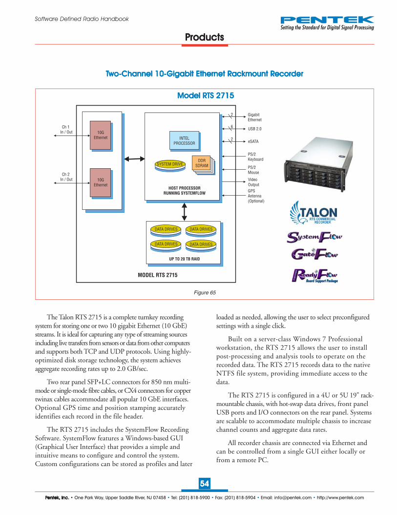
PPPPPentek, Inc.entek, Inc.entek, Inc.entek, Inc.entek, Inc. • One Park Way, Upper Saddle River, NJ 07458 • Tel: (201) 818-5900 • Fax: (201) 818-5904 • Email: [email protected] • http://www.pentek.com
5454545454
Software Defined Radio Handbook
PPPPProductsroductsroductsroductsroducts
Model RTS 2715 Model RTS 2715 Model RTS 2715 Model RTS 2715 Model RTS 2715
Figure 65
TTTTTwowowowowo-----Channel 10-Channel 10-Channel 10-Channel 10-Channel 10-Gigabit Ethernet RGigabit Ethernet RGigabit Ethernet RGigabit Ethernet RGigabit Ethernet Rackmount Rackmount Rackmount Rackmount Rackmount Recorderecorderecorderecorderecorder
Ch 1In / Out 10G
Ethernet INTELPROCESSOR
SYSTEM DRIVEDDR
SDRAM
HOST PROCESSORRUNNING SYSTEMFLOW
UP TO 20 TB RAID
DATA DRIVES DATA DRIVES
DATA DRIVES DATA DRIVES
MODEL RTS 2715
USB 2.0
GigabitEthernet
PS/2Keyboard
PS/2Mouse
VideoOutput
2
6
eSATA2
GPSAntenna(Optional)
Ch 2In / Out 10G
Ethernet
The Talon RTS 2715 is a complete turnkey recordingsystem for storing one or two 10 gigabit Ethernet (10 GbE)streams. It is ideal for capturing any type of streaming sourcesincluding live transfers from sensors or data from other computersand supports both TCP and UDP protocols. Using highly-optimized disk storage technology, the system achievesaggregate recording rates up to 2.0 GB/sec.
Two rear panel SFP+LC connectors for 850 nm multi-mode or single-mode fibre cables, or CX4 connectors for coppertwinax cables accommodate all popular 10 GbE interfaces.Optional GPS time and position stamping accuratelyidentifies each record in the file header.
The RTS 2715 includes the SystemFlow RecordingSoftware. SystemFlow features a Windows-based GUI(Graphical User Interface) that provides a simple andintuitive means to configure and control the system.Custom configurations can be stored as profiles and later
loaded as needed, allowing the user to select preconfiguredsettings with a single click.
Built on a server-class Windows 7 Professionalworkstation, the RTS 2715 allows the user to installpost-processing and analysis tools to operate on therecorded data. The RTS 2715 records data to the nativeNTFS file system, providing immediate access to thedata.
The RTS 2715 is configured in a 4U or 5U 19" rack-mountable chassis, with hot-swap data drives, front panelUSB ports and I/O connectors on the rear panel. Systemsare scalable to accommodate multiple chassis to increasechannel counts and aggregate data rates.
All recorder chassis are connected via Ethernet andcan be controlled from a single GUI either locally orfrom a remote PC.

PPPPPentek, Inc.entek, Inc.entek, Inc.entek, Inc.entek, Inc. • One Park Way, Upper Saddle River, NJ 07458 • Tel: (201) 818-5900 • Fax: (201) 818-5904 • Email: [email protected] • http://www.pentek.com
5555555555
Software Defined Radio Handbook
PPPPProductsroductsroductsroductsroducts
Figure 66
PPPPProductsroductsroductsroductsroducts
Model RTS 2716 Model RTS 2716 Model RTS 2716 Model RTS 2716 Model RTS 2716
Eight-Eight-Eight-Eight-Eight-Channel Serial FPDP RChannel Serial FPDP RChannel Serial FPDP RChannel Serial FPDP RChannel Serial FPDP Rackmount Rackmount Rackmount Rackmount Rackmount Recorderecorderecorderecorderecorder
Ch 1In / Out Serial
FPDP
INTELPROCESSOR
SYSTEM DRIVEDDR
SDRAM
HOST PROCESSORRUNNING SYSTEMFLOW
UP TO 20 TB RAID
DATA DRIVES DATA DRIVES
DATA DRIVES DATA DRIVES
MODEL RTS 2716
USB 2.0
GigabitEthernet
PS/2Keyboard
PS/2Mouse
VideoOutput
2
6
GPSAntenna(Optional)
Ch 2In / Out Serial
FPDP
Ch 3In / Out Serial
FPDP
Ch 4In / Out Serial
FPDP
Ch 5In / Out Serial
FPDP
Ch 6In / Out Serial
FPDP
Ch 7In / Out Serial
FPDP
Ch 8In / Out Serial
FPDP
eSATA2
The Talon RTS 2716 is a complete turnkey recordingsystem capable of recording and playing multiple serialFPDP data streams. It is ideal for capturing any type ofstreaming sources including live transfers from sensorsor data from other computers and is fully compatiblewith the VITA 17.1 specification. Using highly-optimizeddisk storage technology, the system achieves aggregaterecording rates up to 3.4 GB/sec.
The RTS 2716 can be populated with up to eightSFP connectors supporting serial FPDP over copper,single-mode, or multi-mode fiber, to accommodate allpopular serial FPDP interfaces. It is capable of bothreceiving and transmitting data over these links andsupports real-time data storage to disk.
Programmable modes include flow control in bothreceive and transmit directions, CRC support, and copy/loop modes.The system is capable of handling 1.0625,
2.125, 2.5, 3.125 and 4.25 GBaud link rates supporting datatransfer rates of up to 425 MB/sec per serial FPDP link.
Built on a server-class Windows 7 Professional worksta-tion, the RTS 2716 allows the user to install post-processingand analysis tools to operate on the recorded data. TheRTS 2716 records data to the native NTFS file system,providing immediate access to the data.
The RTS 2716 is configured in a 4U or 5U 19" rack-mountable chassis, with hot-swap data drives, front panelUSB ports and I/O connectors on the rear panel. Up to24 hot-swappable SATA drives are optionally available,allowing up to 20 terabytes of real-time data storage spacein a single chassis.
The RTS 2716 includes the SystemFlow RecordingSoftware, which features a Windows-based GUI thatprovides a simple and intuitive means to configure andcontrol the system.

PPPPPentek, Inc.entek, Inc.entek, Inc.entek, Inc.entek, Inc. • One Park Way, Upper Saddle River, NJ 07458 • Tel: (201) 818-5900 • Fax: (201) 818-5904 • Email: [email protected] • http://www.pentek.com
5656565656
Software Defined Radio Handbook
Figure 67
PPPPProductsroductsroductsroductsroducts
FFFFFourourourourour-----Channel RF/IF 200 MS/sec RChannel RF/IF 200 MS/sec RChannel RF/IF 200 MS/sec RChannel RF/IF 200 MS/sec RChannel RF/IF 200 MS/sec Rugged Pugged Pugged Pugged Pugged Pororororortable Rtable Rtable Rtable Rtable Recorderecorderecorderecorderecorder
Model RTR 2726 Model RTR 2726 Model RTR 2726 Model RTR 2726 Model RTR 2726
The Talon RTR 2726 is a turnkey, multiband recordingand playback system designed to operate under conditionsof shock and vibration. It allows the user to record andreproduce high-bandwidth signals with a lightweight,portable and rugged package. The RTR 2726 providessustained recording rates of up to 1.6 GB/sec in a four-channelsystem and is ideal for the user who requires bothportability and solid performance in a compact record-ing system.
The RTR 2726 is supplied in a small footprintportable package measuring just 16.9" W x 9.5" D x13.4" H and weighing about 30 pounds. With measure-ments similar to a small briefcase, this portable workstationincludes an Intel Core i7 processor, a high-resolution17" LCD monitor, and a high-performance SATA RAIDcontroller.
At the heart of the RTR 2726 are Pentek CobaltSeries Virtex-6 software radio boards featuring A/D and
D/A converters, DDCs (Digital Downconverters), DUCs(Digital Upconverters), and complementary FPGA IPcores. This architecture allows the system engineer totake full advantage of the latest technology in a turnkeysystem. Optional GPS time and position stamping allowsthe user to record this critical signal information.
It is built on an extremely rugged, 100% aluminumalloy unit, reinforced with shock absorbing rubber cornersand an impact-resistant protective glass. Using vibrationand shock resistant SSDs, the RTR 2726 is designed toreliably operate as a portable field instrument in harshenvironments.
The eight hot-swappable SSDs provide a storagecapacity of up to 3.8 TB. The drives can be easily removedor exchanged during or after a mission to retrieve recordeddata. Because SSDs operate reliably under conditions ofvibration and shock, the RTR 2726 performs well inground, shipborne and airborne environments.
INTEL CORE i7PROCESSOR
SSDSYSTEM DRIVE
DDRSDRAM
WINDOWS HOST PROCESSOR
RAID DATA STORE
SSD DRIVES SSD DRIVES
SSD DRIVES SSD DRIVES
HIGH RESOLUTIONVIDEO DISPLAY
8x USB 2.0
1x GigabitEthernet
Aux VideoVGA Output
MODEL RTR 2726
ChannelsIn
ChannelsOut
2x eSATA 3
200 MHz16-bit A/D
Up to 4Channels
DIGITAL DOWNCONVERTERDEC: 2 to 64K
800 MHz16-bit D/A
Up to 2Channels
DIGITAL UPCONVERTER
INT: 2 to 512K
2x USB 3.0

PPPPPentek, Inc.entek, Inc.entek, Inc.entek, Inc.entek, Inc. • One Park Way, Upper Saddle River, NJ 07458 • Tel: (201) 818-5900 • Fax: (201) 818-5904 • Email: [email protected] • http://www.pentek.com
5757575757
Software Defined Radio Handbook
Figure 68
PPPPProductsroductsroductsroductsroducts
Model RTR 2727 Model RTR 2727 Model RTR 2727 Model RTR 2727 Model RTR 2727
TTTTTwowowowowo-----Channel RF/IF 500 MS/sec RChannel RF/IF 500 MS/sec RChannel RF/IF 500 MS/sec RChannel RF/IF 500 MS/sec RChannel RF/IF 500 MS/sec Rugged Pugged Pugged Pugged Pugged Pororororortable Rtable Rtable Rtable Rtable Recorderecorderecorderecorderecorder
INTEL CORE i7PROCESSOR
SSDSYSTEM DRIVE
DDRSDRAM
WINDOWS HOST PROCESSOR
RAID DATA STORE
SSD DRIVES SSD DRIVES
SSD DRIVES SSD DRIVES
HIGH RESOLUTIONVIDEO DISPLAY
8x USB 2.0
1x GigabitEthernet
Aux VideoVGA Output
MODEL RTR 2727
ChannelsIn
ChannelOut 2x eSATA 3
DIGITAL DOWN-CONVERTERDEC: 2 to 64K
800 MHz16-bit D/A
Up to 1Channel
500 MHz12-bit A/D
or400 MHz14-bit A/D
Up to 2Channels
DIGITAL UP-CONVERTERINT: 2 to 64K
2x USB 3.0
The Talon RTR 2727 is a turnkey, multiband recordingand playback system designed to operate under conditionsof shock and vibration. It allows the user to record andreproduce high-bandwidth signals with a lightweight,portable and rugged package. The RTR 2727 providessustained recording rates of up to 2.0 GB/sec in a two-channelsystem and is ideal for the user who requires bothportability and solid performance in a compact record-ing system.
The RTR 2727 is supplied in a small footprintportable package measuring just 16.9" W x 9.5" D x13.4" H and weighing about 30 pounds. With measure-ments similar to a small briefcase, this portable workstationincludes an Intel Core i7 processor, a high-resolution17" LCD monitor, and a high-performance SATA RAIDcontroller.
At the heart of the RTR 2727 are Pentek CobaltSeries Virtex-6 software radio boards featuring A/D and
D/A converters, DDCs (Digital Downconverters), DUCs(Digital Upconverters), and complementary FPGA IPcores. This architecture allows the system engineer totake full advantage of the latest technology in a turnkeysystem. Optional GPS time and position stamping allowsthe user to record this critical signal information.
It is built on an extremely rugged, 100% aluminumalloy unit, reinforced with shock absorbing rubber cornersand an impact-resistant protective glass. Using vibrationand shock resistant SSDs, the RTR 2727 is designed toreliably operate as a portable field instrument in harshenvironments.
The eight hot-swappable SSDs provide a storagecapacity of up to 3.8 TB. The drives can be easily removedor exchanged during or after a mission to retrieve recordeddata. Because SSDs operate reliably under conditions ofvibration and shock, the RTR 2727 performs well inground, shipborne and airborne environments.

PPPPPentek, Inc.entek, Inc.entek, Inc.entek, Inc.entek, Inc. • One Park Way, Upper Saddle River, NJ 07458 • Tel: (201) 818-5900 • Fax: (201) 818-5904 • Email: [email protected] • http://www.pentek.com
5858585858
Software Defined Radio Handbook
Figure 69
PPPPProductsroductsroductsroductsroducts
Eight-Eight-Eight-Eight-Eight-Channel Serial FPDP RChannel Serial FPDP RChannel Serial FPDP RChannel Serial FPDP RChannel Serial FPDP Rugged Pugged Pugged Pugged Pugged Pororororortable Rtable Rtable Rtable Rtable Recorderecorderecorderecorderecorder
Model RTR 2736 Model RTR 2736 Model RTR 2736 Model RTR 2736 Model RTR 2736
Ch 1In / Out Serial
FPDP
INTELPROCESSOR
SYSTEM DRIVEDDR
SDRAM
HOST PROCESSORRUNNING SYSTEMFLOW
UP TO 3.8 TB RAID
DATA DRIVES DATA DRIVES
DATA DRIVES DATA DRIVES
MODEL RTR 2736
USB 2.0
GigabitEthernet
PS/2Keyboard
PS/2Mouse
VideoOutput
1
8
eSATA2
GPSAntenna(Optional)
Ch 2In / Out Serial
FPDP
Ch 3In / Out Serial
FPDP
Ch 4In / Out Serial
FPDP
Ch 5In / Out Serial
FPDP
Ch 6In / Out Serial
FPDP
Ch 7In / Out Serial
FPDP
Ch 8In / Out Serial
FPDP
USB 3.02
The Talon RTR 2736 is a complete turnkey recordingsystem designed to operate under conditions of shock andvibration. It records and plays back multiple serial FPDPdata streams in a rugged, lightweight portable package.It is ideal for capturing any type of streaming sourcesincluding live transfers from sensors or data from othercomputers and is fully compatible with the VITA 17.1specification. Using highly-optimized disk storagetechnology, the system achieves aggregate recording ratesup to 1.6 GB/sec.
The RTR 2736 can be populated with up to eightSFP connectors supporting serial FPDP over copper, single-mode, or multi-mode fiber, to accommodate all popularserial FPDP interfaces. It is capable of both receiving andtransmitting data over these links and supports real-time datastorage to disk. The system is capable of handling 1.0625,2.125, 2.5, 3.125 and 4.25 GBaud link rates supportingdata transfer rates of up to 200 MB/sec per serial FPDP link.
The RTR 2736 includes the SystemFlow RecordingSoftware. SystemFlow features a Windows-based GUIthat provides a simple and intuitive means to configureand control the system. Custom configurations can bestored as profiles and later loaded as needed, allowing theuser to select preconfigured settings with a single click.
The RTR 2736 is configured in a portable, lightweightchassis with eight hot-swap SSDs, front panel USB portsand I/O connections on the side panel. It is built on anextremely rugged, 100% aluminum alloy unit, reinforcedwith shock absorbing rubber corners and an impact-resistantprotective glass. Using vibration and shock resistant SSDs,the RTR 2736 is designed to reliably operate as a portablefield instrument in harsh environments.
The eight hot-swappable SSDs provide storagecapacities of up to 3.8 TB. Drives can be easily removedor exchanged during or after a mission to retrieverecorded data.
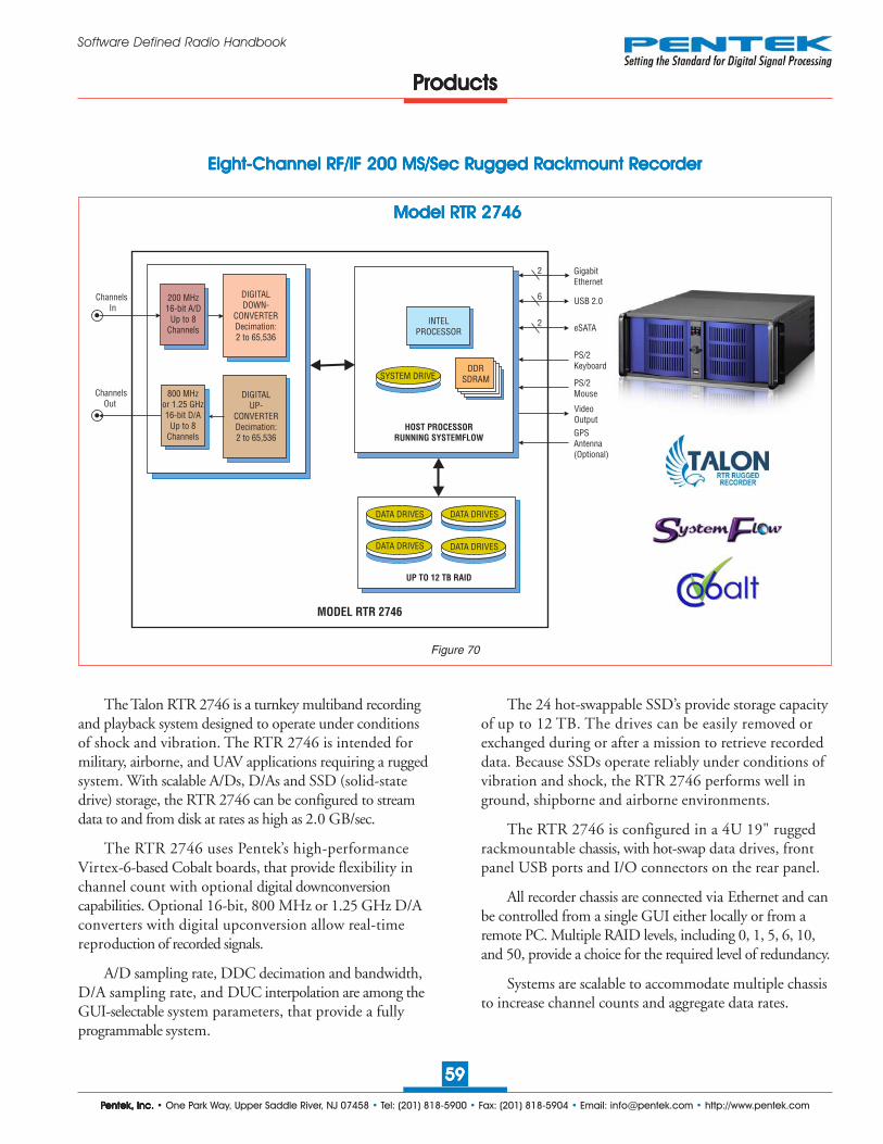
PPPPPentek, Inc.entek, Inc.entek, Inc.entek, Inc.entek, Inc. • One Park Way, Upper Saddle River, NJ 07458 • Tel: (201) 818-5900 • Fax: (201) 818-5904 • Email: [email protected] • http://www.pentek.com
5959595959
Software Defined Radio Handbook
Model RTR 2746 Model RTR 2746 Model RTR 2746 Model RTR 2746 Model RTR 2746
Eight-Eight-Eight-Eight-Eight-Channel RF/IF 200 MS/Sec RChannel RF/IF 200 MS/Sec RChannel RF/IF 200 MS/Sec RChannel RF/IF 200 MS/Sec RChannel RF/IF 200 MS/Sec Rugged Rugged Rugged Rugged Rugged Rackmount Rackmount Rackmount Rackmount Rackmount Recorderecorderecorderecorderecorder
ChannelsIn
ChannelsOut
200 MHz16-bit A/D
Up to 8Channels
DIGITALDOWN-
CONVERTERDecimation:2 to 65,536
INTELPROCESSOR
SYSTEM DRIVEDDR
SDRAM
HOST PROCESSORRUNNING SYSTEMFLOW
UP TO 12 TB RAID
DATA DRIVES DATA DRIVES
DATA DRIVES DATA DRIVES
MODEL RTR 2746
USB 2.0
GigabitEthernet
PS/2Keyboard
PS/2Mouse
VideoOutput
2
6
eSATA2
GPSAntenna(Optional)
800 MHzor 1.25 GHz16-bit D/A
Up to 8Channels
DIGITALUP-
CONVERTERDecimation:2 to 65,536
The Talon RTR 2746 is a turnkey multiband recordingand playback system designed to operate under conditionsof shock and vibration. The RTR 2746 is intended formilitary, airborne, and UAV applications requiring a ruggedsystem. With scalable A/Ds, D/As and SSD (solid-statedrive) storage, the RTR 2746 can be configured to streamdata to and from disk at rates as high as 2.0 GB/sec.
The RTR 2746 uses Pentek’s high-performanceVirtex-6-based Cobalt boards, that provide flexibility inchannel count with optional digital downconversioncapabilities. Optional 16-bit, 800 MHz or 1.25 GHz D/Aconverters with digital upconversion allow real-timereproduction of recorded signals.
A/D sampling rate, DDC decimation and bandwidth,D/A sampling rate, and DUC interpolation are among theGUI-selectable system parameters, that provide a fullyprogrammable system.
The 24 hot-swappable SSD’s provide storage capacityof up to 12 TB. The drives can be easily removed orexchanged during or after a mission to retrieve recordeddata. Because SSDs operate reliably under conditions ofvibration and shock, the RTR 2746 performs well inground, shipborne and airborne environments.
The RTR 2746 is configured in a 4U 19" ruggedrackmountable chassis, with hot-swap data drives, frontpanel USB ports and I/O connectors on the rear panel.
All recorder chassis are connected via Ethernet and canbe controlled from a single GUI either locally or from aremote PC. Multiple RAID levels, including 0, 1, 5, 6, 10,and 50, provide a choice for the required level of redundancy.
Systems are scalable to accommodate multiple chassisto increase channel counts and aggregate data rates.
PPPPProductsroductsroductsroductsroducts
Figure 70

PPPPPentek, Inc.entek, Inc.entek, Inc.entek, Inc.entek, Inc. • One Park Way, Upper Saddle River, NJ 07458 • Tel: (201) 818-5900 • Fax: (201) 818-5904 • Email: [email protected] • http://www.pentek.com
6060606060
Software Defined Radio Handbook
Model RTR 2747 Model RTR 2747 Model RTR 2747 Model RTR 2747 Model RTR 2747
PPPPProductsroductsroductsroductsroducts
Figure 71
FFFFFourourourourour-----Channel RF/IF 500 MS/Sec RChannel RF/IF 500 MS/Sec RChannel RF/IF 500 MS/Sec RChannel RF/IF 500 MS/Sec RChannel RF/IF 500 MS/Sec Rugged Rugged Rugged Rugged Rugged Rackmount Rackmount Rackmount Rackmount Rackmount Recorderecorderecorderecorderecorder
INTELPROCESSOR
SYSTEM DRIVEDDR
SDRAM
HOST PROCESSORRUNNING SYSTEMFLOW
RAID DATA STORE
SSD DRIVES SSD DRIVES
SSD DRIVES SSD DRIVES
MODEL RTR 2747
USB 2.0
GigabitEthernet
PS/2Keyboard
PS/2Mouse
VideoOutput
GPSAntenna(Optional)
ChannelsIn
ChannelsOut
DIGITAL DOWN-CONVERTERDEC: 2 to 64K
800 MHz16-bit D/A
Up to 4Channels
500 MHz12-bit A/D
or400 MHz14-bit A/D
Up to 4Channels
DIGITAL UP-CONVERTERINT: 2 to 64K
The Talon RTR 2747 is a turnkey multiband recordingand playback system designed to operate under conditionsof shock and vibration. The RTR 2747 is intended formilitary, airborne, and UAV applications requiring a ruggedsystem. With scalable A/Ds, D/As and SSD (solid-statedrive) storage, the RTR 2747 can be configured to streamdata to and from disk at rates as high as 4.0 GB/sec.
The RTR 2747 uses Pentek’s high-performanceVirtex-6-based Cobalt boards, that provide flexibility inchannel count with optional digital downconversioncapabilities. Optional 16-bit, 800 MHz converters withdigital upconversion allow real-time reproduction ofrecorded signals.
A/D sampling rate, DDC decimation and bandwidth,D/A sampling rate, and DUC interpolation are among theGUI-selectable system parameters, that provide a fullyprogrammable system.
The hot-swappable SSD’s provide storage capacity ofup to 11.5 TB. The drives can be easily removed orexchanged during or after a mission to retrieve recordeddata. Because SSDs operate reliably under conditions ofvibration and shock, the RTR 2747 performs well inground, shipborne and airborne environments.
The RTR 2747 is configured in a 4U 19" ruggedrackmountable chassis, with hot-swap data drives, frontpanel USB ports and I/O connectors on the rear panel.
All recorder chassis are connected via Ethernet and canbe controlled from a single GUI either locally or from aremote PC. Multiple RAID levels, including 0, 1, 5, 6, 10,and 50, provide a choice for the required level of redundancy.
Systems are scalable to accommodate multiple chassisto increase channel counts and aggregate data rates.

PPPPPentek, Inc.entek, Inc.entek, Inc.entek, Inc.entek, Inc. • One Park Way, Upper Saddle River, NJ 07458 • Tel: (201) 818-5900 • Fax: (201) 818-5904 • Email: [email protected] • http://www.pentek.com
6161616161
Software Defined Radio Handbook
Figure 72
Ultra WUltra WUltra WUltra WUltra Wideband One- or Tideband One- or Tideband One- or Tideband One- or Tideband One- or Twowowowowo-----Channel RF/IFChannel RF/IFChannel RF/IFChannel RF/IFChannel RF/IF, 3.2 GS/sec R, 3.2 GS/sec R, 3.2 GS/sec R, 3.2 GS/sec R, 3.2 GS/sec Rugged Rugged Rugged Rugged Rugged Rackmount Rackmount Rackmount Rackmount Rackmount Recorderecorderecorderecorderecorder
Channel 1In 3.6 GHz
(1 Channel)or
1.8 GHz(2 Channel)12-Bit A/D
INTELPROCESSOR
SYSTEM DRIVEDDR
SDRAM
HOST PROCESSORRUNNING SYSTEMFLOW
UP TO 20 TB RAID
DATA DRIVES DATA DRIVES
DATA DRIVES DATA DRIVES
MODEL RTR 2749
USB
GigabitEthernet
Keyboard
Mouse
VideoOutput
eSATA
GPSAntenna(Optional)
Channel 2In
Designed to operate under conditions of shock andvibration, the Talon RTR 2749 is a turnkey system used forrecording extremely high-bandwidth signals. The RTR 2749uses a 12-bit, 3.6 GHz A/D converter and can providesustained recording rates up to 3.2 GB/sec. It can beconfigured as a one- or two-channel system and can recordsampled data, packed as 8-bit wide consecutive samples,or as 16-bit wide consecutive samples (12-bit digitizedsamples residing in the 12 MSBs of the 16-bit word.)
The RTR 2749 uses Pentek’s high-performanceVirtex-6-based Cobalt boards that provide the datastreaming engine for the high-speed A/D converter.Channel and packing modes as well as gate and triggersettings are among the GUI-selectable system parameters,providing complete control over this ultra-widebandrecording system. Optional GPS time and position stampingallows the user to capture this information in the header ofeach data file.
The RTR 2749 includes the SystemFlow RecordingSoftware. SystemFlow features a Windows-based GUIthat provides a simple means to configure and control thesystem. Custom configurations can be stored as profilesand later loaded when needed, allowing the user to selectpreconfigured settings with a single click. SystemFlowalso includes signal viewing and analysis tools that allowthe user to monitor the signal prior to, during, and aftera recording session.
Built on a Windows 7 Professional workstation,the RTR 2749 allows the user to install post-processingand analysis tools to operate on the recorded data.The hot-swappable SSDs provide a storage capacity of upto 19.2 TB. The drives can be easily removed or exchangedduring or after a mission to retrieve recorded data. BecauseSSDs operate reliably under conditions of vibrationand shock, the RTR 2749 performs well in ground,shipborne and airborne environments.
Model RTR 2749 Model RTR 2749 Model RTR 2749 Model RTR 2749 Model RTR 2749
PPPPProductsroductsroductsroductsroducts
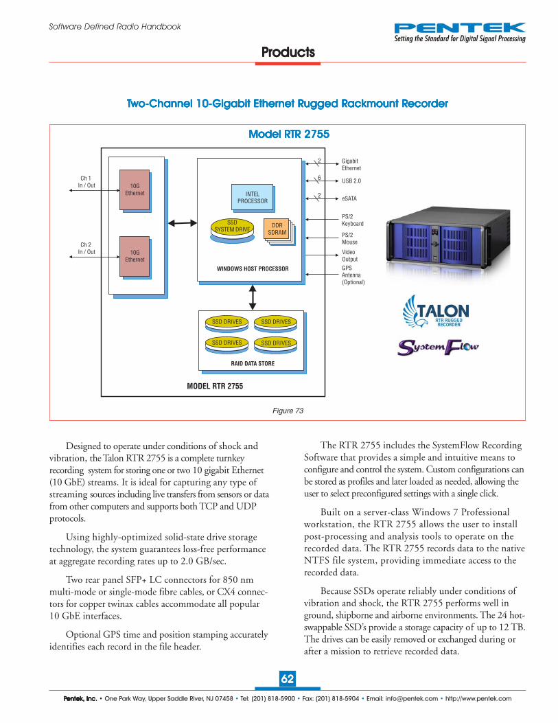
PPPPPentek, Inc.entek, Inc.entek, Inc.entek, Inc.entek, Inc. • One Park Way, Upper Saddle River, NJ 07458 • Tel: (201) 818-5900 • Fax: (201) 818-5904 • Email: [email protected] • http://www.pentek.com
6262626262
Software Defined Radio Handbook
PPPPProductsroductsroductsroductsroducts
Model RTR 2755 Model RTR 2755 Model RTR 2755 Model RTR 2755 Model RTR 2755
TTTTTwowowowowo-----Channel 10-Channel 10-Channel 10-Channel 10-Channel 10-Gigabit Ethernet RGigabit Ethernet RGigabit Ethernet RGigabit Ethernet RGigabit Ethernet Rugged Rugged Rugged Rugged Rugged Rackmount Rackmount Rackmount Rackmount Rackmount Recorderecorderecorderecorderecorder
The RTR 2755 includes the SystemFlow RecordingSoftware that provides a simple and intuitive means toconfigure and control the system. Custom configurations canbe stored as profiles and later loaded as needed, allowing theuser to select preconfigured settings with a single click.
Built on a server-class Windows 7 Professionalworkstation, the RTR 2755 allows the user to installpost-processing and analysis tools to operate on therecorded data. The RTR 2755 records data to the nativeNTFS file system, providing immediate access to therecorded data.
Because SSDs operate reliably under conditions ofvibration and shock, the RTR 2755 performs well inground, shipborne and airborne environments. The 24 hot-swappable SSD’s provide a storage capacity of up to 12 TB.The drives can be easily removed or exchanged during orafter a mission to retrieve recorded data.
Figure 73
Ch 1In / Out 10G
Ethernet INTELPROCESSOR
SSDSYSTEM DRIVE
DDRSDRAM
WINDOWS HOST PROCESSOR
RAID DATA STORE
SSD DRIVES SSD DRIVES
SSD DRIVES SSD DRIVES
MODEL RTR 2755
USB 2.0
GigabitEthernet
PS/2Keyboard
PS/2Mouse
VideoOutput
2
6
eSATA2
GPSAntenna(Optional)
Ch 2In / Out 10G
Ethernet
Designed to operate under conditions of shock andvibration, the Talon RTR 2755 is a complete turnkeyrecording system for storing one or two 10 gigabit Ethernet(10 GbE) streams. It is ideal for capturing any type ofstreaming sources including live transfers from sensors or datafrom other computers and supports both TCP and UDPprotocols.
Using highly-optimized solid-state drive storagetechnology, the system guarantees loss-free performanceat aggregate recording rates up to 2.0 GB/sec.
Two rear panel SFP+ LC connectors for 850 nmmulti-mode or single-mode fibre cables, or CX4 connec-tors for copper twinax cables accommodate all popular10 GbE interfaces.
Optional GPS time and position stamping accuratelyidentifies each record in the file header.
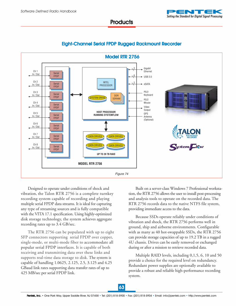
PPPPPentek, Inc.entek, Inc.entek, Inc.entek, Inc.entek, Inc. • One Park Way, Upper Saddle River, NJ 07458 • Tel: (201) 818-5900 • Fax: (201) 818-5904 • Email: [email protected] • http://www.pentek.com
6363636363
Software Defined Radio Handbook
PPPPProductsroductsroductsroductsroducts
Model RTR 2756 Model RTR 2756 Model RTR 2756 Model RTR 2756 Model RTR 2756
Eight-Eight-Eight-Eight-Eight-Channel Serial FPDP RChannel Serial FPDP RChannel Serial FPDP RChannel Serial FPDP RChannel Serial FPDP Rugged Rugged Rugged Rugged Rugged Rackmount Rackmount Rackmount Rackmount Rackmount Recorderecorderecorderecorderecorder
Figure 74
Ch 1In / Out Serial
FPDP
INTELPROCESSOR
SYSTEM DRIVEDDR
SDRAM
HOST PROCESSORRUNNING SYSTEMFLOW
UP TO 20 TB RAID
DATA DRIVES DATA DRIVES
DATA DRIVES DATA DRIVES
MODEL RTR 2756
USB 2.0
GigabitEthernet
PS/2Keyboard
PS/2Mouse
VideoOutput
2
6
GPSAntenna(Optional)
Ch 2In / Out Serial
FPDP
Ch 3In / Out Serial
FPDP
Ch 4In / Out Serial
FPDP
Ch 5In / Out Serial
FPDP
Ch 6In / Out Serial
FPDP
Ch 7In / Out Serial
FPDP
Ch 8In / Out Serial
FPDP
eSATA2
Designed to operate under conditions of shock andvibration, the Talon RTR 2756 is a complete turnkeyrecording system capable of recording and playingmultiple serial FPDP data streams. It is ideal for capturingany type of streaming sources and is fully compatiblewith the VITA 17.1 specification. Using highly-optimizeddisk storage technology, the system achieves aggregaterecording rates up to 3.4 GB/sec.
The RTR 2756 can be populated with up to eightSFP connectors supporting serial FPDP over copper,single-mode, or multi-mode fiber to accommodate allpopular serial FPDP interfaces. It is capable of bothreceiving and transmitting data over these links andsupports real-time data storage to disk. The system iscapable of handling 1.0625, 2.125, 2.5, 3.125 and 4.25GBaud link rates supporting data transfer rates of up to425 MB/sec per serial FPDP link.
Built on a server-class Windows 7 Professional worksta-tion, the RTR 2756 allows the user to install post-processingand analysis tools to operate on the recorded data. TheRTR 2756 records data to the native NTFS file system,providing immediate access to the data.
Because SSDs operate reliably under conditions ofvibration and shock, the RTR 2756 performs well inground, ship and airborne environments. Configurablewith as many as 40 hot-swappable SSDs, the RTR 2756can provide storage capacities of up to 19.2 TB in a rugged4U chassis. Drives can be easily removed or exchangedduring or after a mission to retrieve recorded data.
Multiple RAID levels, including 0,1,5, 6, 10 and 50provide a choice for the required level on redundancy.Redundant power supplies are optionally available toprovide a robust and reliable high-performance recordingsystem.

PPPPPentek, Inc.entek, Inc.entek, Inc.entek, Inc.entek, Inc. • One Park Way, Upper Saddle River, NJ 07458 • Tel: (201) 818-5900 • Fax: (201) 818-5904 • Email: [email protected] • http://www.pentek.com
6464646464
Software Defined Radio Handbook
PPPPProductsroductsroductsroductsroducts
Model RTX 2786 Model RTX 2786 Model RTX 2786 Model RTX 2786 Model RTX 2786
Figure 75
FFFFFourourourourour-----Channel RF/IF 200 MS/Sec Extreme 3U VPX RChannel RF/IF 200 MS/Sec Extreme 3U VPX RChannel RF/IF 200 MS/Sec Extreme 3U VPX RChannel RF/IF 200 MS/Sec Extreme 3U VPX RChannel RF/IF 200 MS/Sec Extreme 3U VPX Recorderecorderecorderecorderecorder
CH 1In
200 MHz16-bit A/D
MODEL53621
Out
Sample Clk /Reference In
CLOCK &SYNC
GENERATOR
PROGRAMVCXO
DIGITALDOWN-
CONVERTER
DIGITALUPCONVERTER
INTELPROCESSOR
SYSTEM DRIVE
A
DDRSDRAM
HOST PROCESSOR
RAID
DATA DRIVES DATA DRIVES
DATA DRIVES DATA DRIVES
MODEL RTX 2786
USB 2.0
GigabitEthernet
VideoOutput
CH 2In
200 MHz16-bit A/D
DIGITALDOWN-
CONVERTER
CH 3In
200 MHz16-bit A/D
DIGITALDOWN-
CONVERTER
A
2
4
Three Record Channels and One Playback Channel.
800 MHz16-bit D/A
The Talon RTX 2786 is a turnkey, RF/IF signalrecorder designed to operate under extreme environmen-tal conditions. Housed in a ½ ATR chassis, the RTX2786 leverages Pentek’s 3U VPX SDR modules to provide arugged recording system with up to four 16-bit, 200 MHzA/D converters with built-in digital downconversioncapabilities. Optionally, the RTX 2786 provides one800 MHz, 16-bit D/A converter with a digital upconverterfor signal playback or waveform generation. As shown inthe block diagram, the maximum number of record channelswith this option is three.
The RTX 2786 uses conduction cooling to draw heatfrom the system components allowing it to operate in reducedair environments. It includes 1.92 TB of solid-state datastorage, that allows it to operate with no degradation underconditions of extreme shock and vibration. The system ishermetically sealed and provides five D38999 connectorsfor power and I/O with four SMA connectors for analog I/O.
The RTX 2786 includes Pentek’s SystemFlowRecording Software. SystemFlow features a Windows-based GUI that provides a simple means to configureand control the system. Custom configurations can bestored as profiles and later loaded when needed, allowingthe user to select preconfigured settings with a single click.SystemFlow also includes signal viewing and analysistools, that allow the user to monitor the signal prior to,during, and after a recording session. These tools include avirtual oscilloscope and a virtual spectrum analyzer.
The user API allows users to integrate the recorder asa subsystem of a larger system. The API is provided as a C-callable library and allows for the recorder to be controlledover Ethernet, thus providing the ability to remotelycontrol the recorder from a custom interface.
Four built-in solid-state drives provide reliable, high-speed storage with a total capacity of 1.92 TB.
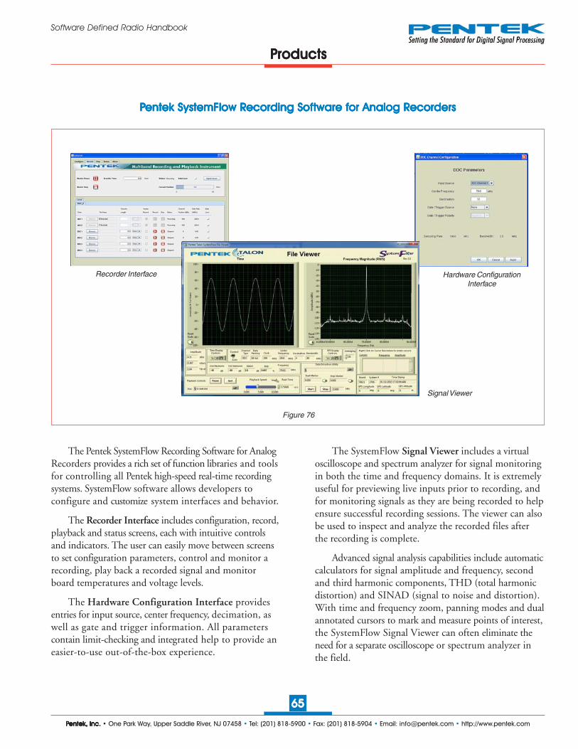
PPPPPentek, Inc.entek, Inc.entek, Inc.entek, Inc.entek, Inc. • One Park Way, Upper Saddle River, NJ 07458 • Tel: (201) 818-5900 • Fax: (201) 818-5904 • Email: [email protected] • http://www.pentek.com
6565656565
Software Defined Radio Handbook
PPPPPentek SystemFlow Rentek SystemFlow Rentek SystemFlow Rentek SystemFlow Rentek SystemFlow Recording Sofecording Sofecording Sofecording Sofecording Software for Analog Rtware for Analog Rtware for Analog Rtware for Analog Rtware for Analog Recordersecordersecordersecordersecorders
Figure 76
Signal Viewer
Recorder Interface Hardware ConfigurationInterface
The Pentek SystemFlow Recording Software for AnalogRecorders provides a rich set of function libraries and toolsfor controlling all Pentek high-speed real-time recordingsystems. SystemFlow software allows developers toconfigure and customize system interfaces and behavior.
The Recorder Interface includes configuration, record,playback and status screens, each with intuitive controlsand indicators. The user can easily move between screensto set configuration parameters, control and monitor arecording, play back a recorded signal and monitorboard temperatures and voltage levels.
The Hardware Configuration Interface providesentries for input source, center frequency, decimation, aswell as gate and trigger information. All parameterscontain limit-checking and integrated help to provide aneasier-to-use out-of-the-box experience.
The SystemFlow Signal Viewer includes a virtualoscilloscope and spectrum analyzer for signal monitoringin both the time and frequency domains. It is extremelyuseful for previewing live inputs prior to recording, andfor monitoring signals as they are being recorded to helpensure successful recording sessions. The viewer can alsobe used to inspect and analyze the recorded files afterthe recording is complete.
Advanced signal analysis capabilities include automaticcalculators for signal amplitude and frequency, secondand third harmonic components, THD (total harmonicdistortion) and SINAD (signal to noise and distortion).With time and frequency zoom, panning modes and dualannotated cursors to mark and measure points of interest,the SystemFlow Signal Viewer can often eliminate theneed for a separate oscilloscope or spectrum analyzer inthe field.
PPPPProductsroductsroductsroductsroducts

PPPPPentek, Inc.entek, Inc.entek, Inc.entek, Inc.entek, Inc. • One Park Way, Upper Saddle River, NJ 07458 • Tel: (201) 818-5900 • Fax: (201) 818-5904 • Email: [email protected] • http://www.pentek.com
6666666666
Software Defined Radio Handbook
PPPPPentek SystemFlow Rentek SystemFlow Rentek SystemFlow Rentek SystemFlow Rentek SystemFlow Recording Sofecording Sofecording Sofecording Sofecording Software for Digital Rtware for Digital Rtware for Digital Rtware for Digital Rtware for Digital Recordersecordersecordersecordersecorders
Figure 77
PPPPProductsroductsroductsroductsroducts
The SystemFlow Software for Digital Resordersprovides the user with a control interface for the recordingsystem. It includes Configuration, Record, Playback, andStatus screens, each with intuitive controls and indicators.
The user can easily move between screens to setconfiguration parameters, control and monitor a recording,and play back a recorded stream. All parameters containlimit-checking and integrated help to provide an easier-to-use out-of-the-box experience.
The Configure Screen shows a block diagram ofthe system, and presents operational system parametersincluding temperature and voltages. Parameters areentered for each input or output channel specifyingUDP or TCP protocol, client or server connection, theIP address and port number.
The Recording and Playback Screen allows you tobrowse a folder and enter a file name for the recording.The length of the recording for each channel can bespecified in megabytes or in seconds. Intuitive buttonsfor Record, Pause and Stop simplify operation. Statusindicators for each channel display the mode, the numberof recorded bytes, and the average data rate. A Data Lossindicator alerts the user to any problem, such as a disk-full condition.
By checking the Master Record boxes, any combina-tion of channels in the lower screen can be grouped forsynchronous recording via the upper Master Record screen.The recording time can be specified, and monitoringfunctions inform the operator of recording progress.
Recording and Playback Screen
Configure Screen
Hardware Configuration
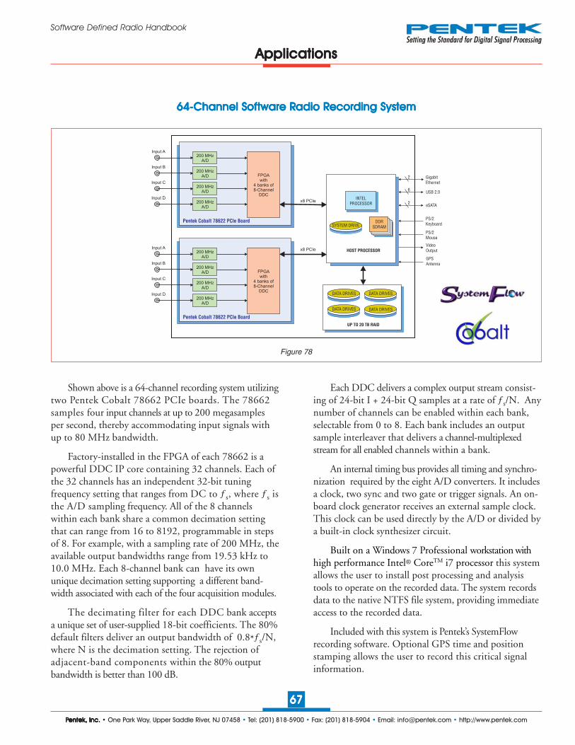
PPPPPentek, Inc.entek, Inc.entek, Inc.entek, Inc.entek, Inc. • One Park Way, Upper Saddle River, NJ 07458 • Tel: (201) 818-5900 • Fax: (201) 818-5904 • Email: [email protected] • http://www.pentek.com
6767676767
Software Defined Radio Handbook
ApplicationsApplicationsApplicationsApplicationsApplications
Figure 78
INTELPROCESSOR
SYSTEM DRIVEDDR
SDRAM
HOST PROCESSOR
UP TO 20 TB RAID
DATA DRIVES DATA DRIVES
DATA DRIVES DATA DRIVES
USB 2.0
GigabitEthernet
PS/2Keyboard
PS/2Mouse
VideoOutput
2
6
eSATA2
GPSAntenna
x8 PCIe
x8 PCIe
Input A
Input B
Input C
Input D
200 MHzA/D
200 MHzA/D
200 MHzA/D
200 MHzA/D
FPGAwith
4 banks of8-Channel
DDC
Pentek Cobalt 78622 PCIe Board
Input A
Input B
Input C
Input D
200 MHzA/D
200 MHzA/D
200 MHzA/D
200 MHzA/D
FPGAwith
4 banks of8-Channel
DDC
Pentek Cobalt 78622 PCIe Board
64-64-64-64-64-Channel SofChannel SofChannel SofChannel SofChannel Software Rtware Rtware Rtware Rtware Radio Radio Radio Radio Radio Recording Systemecording Systemecording Systemecording Systemecording System
Each DDC delivers a complex output stream consist-ing of 24-bit I + 24-bit Q samples at a rate of ƒs/N. Anynumber of channels can be enabled within each bank,selectable from 0 to 8. Each bank includes an outputsample interleaver that delivers a channel-multiplexedstream for all enabled channels within a bank.
An internal timing bus provides all timing and synchro-nization required by the eight A/D converters. It includesa clock, two sync and two gate or trigger signals. An on-board clock generator receives an external sample clock.This clock can be used directly by the A/D or divided bya built-in clock synthesizer circuit.
Built on a Windows 7 Professional workstation withhigh performance Intel® CoreTM i7 processor this systemallows the user to install post processing and analysistools to operate on the recorded data. The system recordsdata to the native NTFS file system, providing immediateaccess to the recorded data.
Included with this system is Pentek’s SystemFlowrecording software. Optional GPS time and positionstamping allows the user to record this critical signalinformation.
Shown above is a 64-channel recording system utilizingtwo Pentek Cobalt 78662 PCIe boards. The 78662samples four input channels at up to 200 megasamplesper second, thereby accommodating input signals withup to 80 MHz bandwidth.
Factory-installed in the FPGA of each 78662 is apowerful DDC IP core containing 32 channels. Each ofthe 32 channels has an independent 32-bit tuningfrequency setting that ranges from DC to ƒs, where ƒs isthe A/D sampling frequency. All of the 8 channelswithin each bank share a common decimation settingthat can range from 16 to 8192, programmable in stepsof 8. For example, with a sampling rate of 200 MHz, theavailable output bandwidths range from 19.53 kHz to10.0 MHz. Each 8-channel bank can have its ownunique decimation setting supporting a different band-width associated with each of the four acquisition modules.
The decimating filter for each DDC bank acceptsa unique set of user-supplied 18-bit coefficients. The 80%default filters deliver an output bandwidth of 0.8*ƒs/N,where N is the decimation setting. The rejection ofadjacent-band components within the 80% outputbandwidth is better than 100 dB.
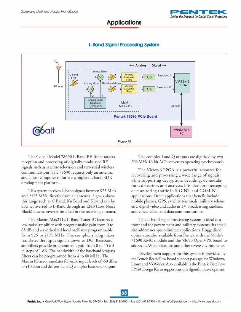
PPPPPentek, Inc.entek, Inc.entek, Inc.entek, Inc.entek, Inc. • One Park Way, Upper Saddle River, NJ 07458 • Tel: (201) 818-5900 • Fax: (201) 818-5904 • Email: [email protected] • http://www.pentek.com
6868686868
Software Defined Radio Handbook
LLLLL-Band Signal P-Band Signal P-Band Signal P-Band Signal P-Band Signal Processing Systemrocessing Systemrocessing Systemrocessing Systemrocessing System
ApplicationsApplicationsApplicationsApplicationsApplications
The Cobalt Model 78690 L-Band RF Tuner targetsreception and processing of digitally-modulated RFsignals such as satellite television and terrestrial wirelesscommunications. The 78690 requires only an antennaand a host computer to form a complete L-band SDRdevelopment platform.
This system receives L-Band signals between 925 MHzand 2175 MHz directly from an antenna. Signals abovethis range such as C Band, Ku Band and K band can bedownconverted to L-Band through an LNB (Low NoiseBlock) downconverter installed in the receiving antenna.
The Maxim Max2112 L-Band Tuner IC features alow-noise amplifier with programmable gain from 0 to65 dB and a synthesized local oscillator programmablefrom 925 to 2175 MHz. The complex analog mixertranslates the input signals down to DC. Basebandamplifiers provide programmable gain from 0 to 15 dBin steps of 1 dB. The bandwidth of the baseband lowpassfilters can be programmed from 4 to 40 MHz . TheMaxim IC accommodates full-scale input levels of -50 dBmto +10 dbm and delivers I and Q complex baseband outputs.
Figure 79
Analog Digital
Baseband IL-Band
x8 PCIe
LNA
Analog Local
Oscillator
Synthesizer
Q
Baseband AmpsAnalog Mixer
Analog Mixer
I
AnalogLowpass
FilterA/D
A/D
FPGA
VIRTEX-6
PC
WINDOWS
RF Input Baseband Q
MaximMAX2112
Pentek 78690 PCIe Board
LowpassFilter
Analog
The complex I and Q outputs are digitized by two200 MHz 16-bit A/D converters operating synchronously.
The Virtex-6 FPGA is a powerful resource forrecovering and processing a wide range of signalswhile supporting decryption, decoding, demodula-tion, detection, and analysis. It is ideal for interceptingor monitoring traffic in SIGINT and COMINTapplications. Other applications that benefit includemobile phones, GPS, satellite terminals, military telem-etry, digital video and audio in TV broadcasting satellites,and voice, video and data communications.
This L-Band signal processing system is ideal as afront end for government and military systems. Its smallsize adderesses space-limited applications. Ruggedizedoptions are also available from Pentek with the Models71690 XMC module and the 53690 OpenVPX board toaddress UAV applications and other severe environments.
Development support for this system is provided bythe Pentek ReadyFlow board support package for Windows,Linux and VxWorks. Also available is the Pentek GateFlowFPGA Design Kit to support custom algorithm development.
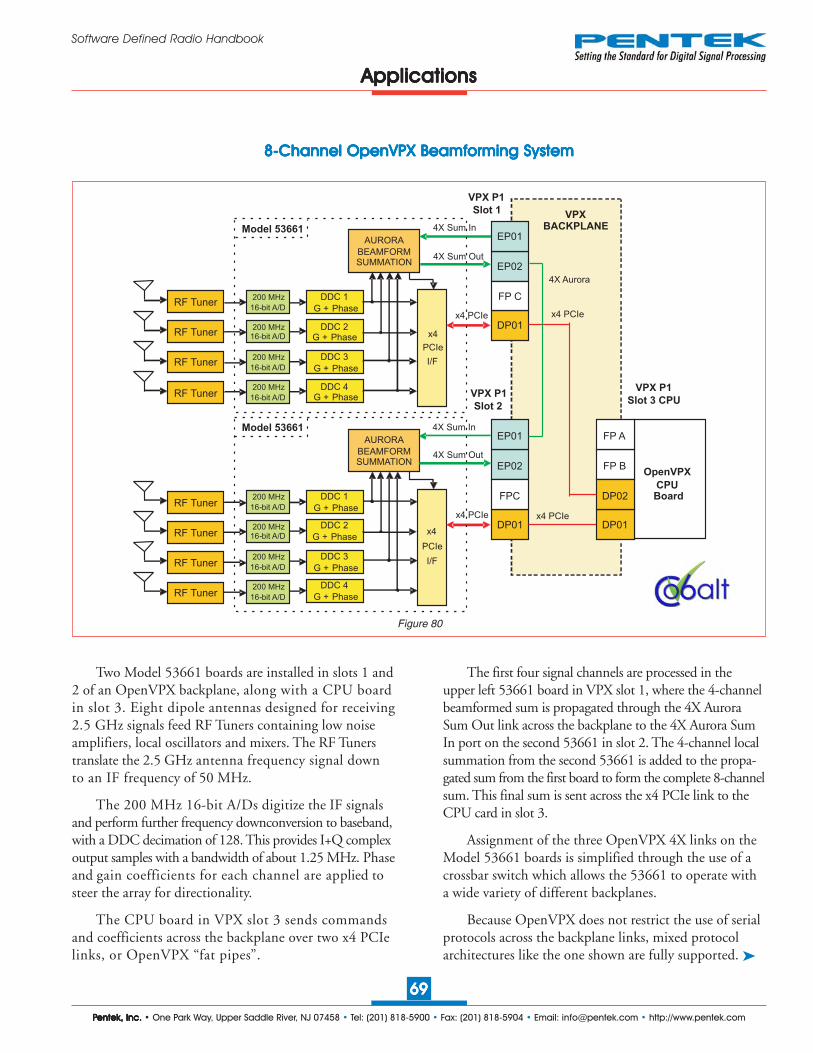
PPPPPentek, Inc.entek, Inc.entek, Inc.entek, Inc.entek, Inc. • One Park Way, Upper Saddle River, NJ 07458 • Tel: (201) 818-5900 • Fax: (201) 818-5904 • Email: [email protected] • http://www.pentek.com
6969696969
Software Defined Radio Handbook
ApplicationsApplicationsApplicationsApplicationsApplications
Figure 80
8-8-8-8-8-Channel OpenVPX Beamforming SystemChannel OpenVPX Beamforming SystemChannel OpenVPX Beamforming SystemChannel OpenVPX Beamforming SystemChannel OpenVPX Beamforming System
Two Model 53661 boards are installed in slots 1 and2 of an OpenVPX backplane, along with a CPU boardin slot 3. Eight dipole antennas designed for receiving2.5 GHz signals feed RF Tuners containing low noiseamplifiers, local oscillators and mixers. The RF Tunerstranslate the 2.5 GHz antenna frequency signal downto an IF frequency of 50 MHz.
The 200 MHz 16-bit A/Ds digitize the IF signalsand perform further frequency downconversion to baseband,with a DDC decimation of 128. This provides I+Q complexoutput samples with a bandwidth of about 1.25 MHz. Phaseand gain coefficients for each channel are applied tosteer the array for directionality.
The CPU board in VPX slot 3 sends commandsand coefficients across the backplane over two x4 PCIelinks, or OpenVPX “fat pipes”.
The first four signal channels are processed in theupper left 53661 board in VPX slot 1, where the 4-channelbeamformed sum is propagated through the 4X AuroraSum Out link across the backplane to the 4X Aurora SumIn port on the second 53661 in slot 2. The 4-channel localsummation from the second 53661 is added to the propa-gated sum from the first board to form the complete 8-channelsum. This final sum is sent across the x4 PCIe link to theCPU card in slot 3.
Assignment of the three OpenVPX 4X links on theModel 53661 boards is simplified through the use of acrossbar switch which allows the 53661 to operate witha wide variety of different backplanes.
Because OpenVPX does not restrict the use of serialprotocols across the backplane links, mixed protocolarchitectures like the one shown are fully supported. ➤
VPX P1
Slot 1
EP02
EP01
DP01
FP C
VPX P1
Slot 2
VPX P1
Slot 3 CPU
EP02
EP01
DP01
FPC
x4 PCIe
x4 PCIe
200 MHz
16-bit A/D
DDC 4G + Phase
PCIe
x4
I/F
200 MHz16-bit A/D
200 MHz
16-bit A/D
200 MHz
16-bit A/D
AURORA
BEAMFORMSUMMATION
DDC 3
G + Phase
DDC 2G + Phase
DDC 1
G + Phase
4X Sum In
4X Sum Out
Model 53661
x4 PCIe
200 MHz
16-bit A/D
DDC 4
G + Phase
PCIe
x4
I/F
200 MHz16-bit A/D
200 MHz
16-bit A/D
200 MHz
16-bit A/D
AURORA
BEAMFORMSUMMATION
DDC 3
G + Phase
DDC 2
G + Phase
DDC 1
G + Phase
4X Sum In
4X Sum Out
x4 PCIe
Model 53661
RF Tuner
RF Tuner
RF Tuner
RF Tuner
RF Tuner
RF Tuner
RF Tuner
RF Tuner
FP B
FP A
DP01
DP02
OpenVPX
CPUBoard
VPXBACKPLANE
4X Aurora
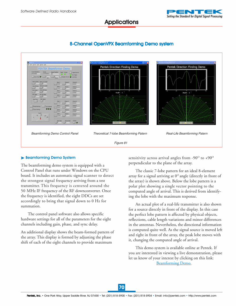
PPPPPentek, Inc.entek, Inc.entek, Inc.entek, Inc.entek, Inc. • One Park Way, Upper Saddle River, NJ 07458 • Tel: (201) 818-5900 • Fax: (201) 818-5904 • Email: [email protected] • http://www.pentek.com
7070707070
Software Defined Radio Handbook
ApplicationsApplicationsApplicationsApplicationsApplications
Figure 81
8-8-8-8-8-Channel OpenVPX Beamforming Demo systemChannel OpenVPX Beamforming Demo systemChannel OpenVPX Beamforming Demo systemChannel OpenVPX Beamforming Demo systemChannel OpenVPX Beamforming Demo system
➤➤➤➤➤ Beamforming Demo System
The beamforming demo system is equipped with aControl Panel that runs under Windows on the CPUboard. It includes an automatic signal scanner to detectthe strongest signal frequency arriving from a testtransmitter. This frequency is centered around the50 MHz IF frequency of the RF downconverter. Oncethe frequency is identified, the eight DDCs are setaccordingly to bring that signal down to 0 Hz forsummation.
The control panel software also allows specifichardware settings for all of the parameters for the eightchannels including gain, phase, and sync delay.
An additional display shows the beam-formed pattern ofthe array. This display is formed by adjusting the phaseshift of each of the eight channels to provide maximum
sensitivity across arrival angles from -90O to +90O
perpendicular to the plane of the array.
The classic 7-lobe pattern for an ideal 8-elementarray for a signal arriving at 0O angle (directly in front ofthe array) is shown above. Below the lobe pattern is apolar plot showing a single vector pointing to thecomputed angle of arrival. This is derived from identify-ing the lobe with the maximum response.
An actual plot of a real-life transmitter is also shownfor a source directly in front of the display. In this casethe perfect lobe pattern is affected by physical objects,reflections, cable length variations and minor differencesin the antennas. Nevertheless, the directional informationis computed quite well. As the signal source is moved leftand right in front of the array, the peak lobe moves withit, changing the computed angle of arrival.
This demo system is available online at Pentek. Ifyou are interested in viewing a live demonstration, pleaselet us know of your interest by clicking on this link:
Beamforming Demo.
Beamforming Demo Control Panel Theoretical 7-lobe Beamforming Patern Real-Life Beamforming Patern

PPPPPentek, Inc.entek, Inc.entek, Inc.entek, Inc.entek, Inc. • One Park Way, Upper Saddle River, NJ 07458 • Tel: (201) 818-5900 • Fax: (201) 818-5904 • Email: [email protected] • http://www.pentek.com
7171717171
Software Defined Radio Handbook
More links on the next page ➤
The following links provide you with additional information about the Pentek productspresented in this handbook: just click on the model number. Links are also provided to otherhandbooks or catalogs that may be of interest in your software radio development projects.
ModelModelModelModelModel DescriptionDescriptionDescriptionDescriptionDescription PPPPPageageageageage
7142 Multichannel Transceiver with Virtex-4 FPGAs - PMC/XMC 197242 Multichannel Transceiver with Virtex-4 FPGAs - 6U cPCI 197342 Multichannel Transceiver with Virtex-4 FPGAs - 3U cPCI 197642 Multichannel Transceiver with Virtex-4 FPGAs - PCI 197742 Multichannel Transceiver with Virtex-4 FPGAs - Full-length PCIe 197842 Multichannel Transceiver with Virtex-4 FPGAs - Half-length PCIe 195342 Multichannel Transceiver with Virtex-4 FPGAs - 3U VPX 197142-428 Multichannel Transceiver w. Four Multiband DDCs and Interpolation Filter - PMC/XMC 207242-428 Multichannel Transceiver w. Four Multiband DDCs and Interpolation Filter- 6U cPCI 207342-428 Multichannel Transceiver w. Four Multiband DDCs and Interpolation Filter- 3U cPCI 207642-428 Multichannel Transceiver w. Four Multiband DDCs and Interpolation Filter- PCI 207742-428 Multichannel Transceiver w. Four Multiband DDCs and Interpolation Filter- Full-length PCIe 207842-428 Multichannel Transceiver w. Four Multiband DDCs and Interpolation Filter- Half-length PCIe 205342-428 Multichannel Transceiver w. Four Multiband DDCs and Interpolation Filter- 3U VPX 207150 Quad 200 MHz, 16-bit A/D with Virtex-5 FPGAs - PMC/XMC 217250 Quad 200 MHz, 16-bit A/D with Virtex-5 FPGAs - 6U cPCI 217350 Quad 200 MHz, 16-bit A/D with Virtex-5 FPGAs - 3U cPCI 217650 Quad 200 MHz, 16-bit A/D with Virtex-5 FPGAs - PCI 217750 Quad 200 MHz, 16-bit A/D with Virtex-5 FPGAs - Full-length PCIe 217850 Quad 200 MHz, 16-bit A/D with Virtex-5 FPGAs - Half-length PCIe 215350 Quad 200 MHz, 16-bit A/D with Virtex-5 FPGAs - 3U VPX 217151 256-Channel DDC with Quad 200 MHz, 16-bit A/D - PMC 227251 256-Channel DDC with Quad 200 MHz, 16-bit A/D - 6U cPCI 227351 256-Channel DDC with Quad 200 MHz, 16-bit A/D - 3U cPCI 227651 256-Channel DDC with Quad 200 MHz, 16-bit A/D - PCI 227751 256-Channel DDC with Quad 200 MHz, 16-bit A/D - Full-length PCIe 227851 256-Channel DDC with Quad 200 MHz, 16-bit A/D - Half-length PCIe 225351 256-Channel DDC with Quad 200 MHz, 16-bit A/D - 3U VPX 227152 32-Channel DDC with Quad 200 MHz, 16-bit A/D - PMC 237252 32-Channel DDC with Quad 200 MHz, 16-bit A/D - 6U cPCI 237352 32-Channel DDC with Quad 200 MHz, 16-bit A/D - 3U cPCI 237652 32-Channel DDC with Quad 200 MHz, 16-bit A/D - PCI 237752 32-Channel DDC with Quad 200 MHz, 16-bit A/D - Full-length PCIe 237852 32-Channel DDC with Quad 200 MHz, 16-bit A/D - Half-length PCIe 235352 32-Channel DDC with Quad 200 MHz, 16-bit A/D - 3U VPX 237153 4-Channel DDC with Quad 200 MHz, 16-bit A/D - PMC/XMC 247253 4-Channel DDC with Quad 200 MHz, 16-bit A/D - 6U cPCI 247353 4-Channel DDC with Quad 200 MHz, 16-bit A/D - 3U cPCI 247653 4-Channel DDC with Quad 200 MHz, 16-bit A/D - PCI 247753 4-Channel DDC with Quad 200 MHz, 16-bit A/D - Full-length PCIe 247853 4-Channel DDC with Quad 200 MHz, 16-bit A/D - Half-length PCIe 245353 4-Channel DDC with Quad 200 MHz, 16-bit A/D - 3U VPX 24
LinksLinksLinksLinksLinks
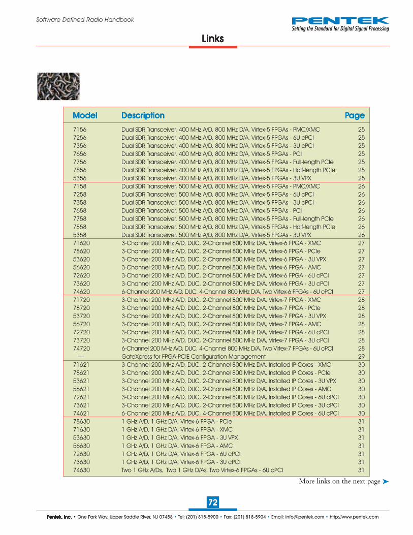
PPPPPentek, Inc.entek, Inc.entek, Inc.entek, Inc.entek, Inc. • One Park Way, Upper Saddle River, NJ 07458 • Tel: (201) 818-5900 • Fax: (201) 818-5904 • Email: [email protected] • http://www.pentek.com
7272727272
Software Defined Radio Handbook
ModelModelModelModelModel DescriptionDescriptionDescriptionDescriptionDescription PPPPPageageageageage
7156 Dual SDR Transceiver, 400 MHz A/D, 800 MHz D/A, Virtex-5 FPGAs - PMC/XMC 257256 Dual SDR Transceiver, 400 MHz A/D, 800 MHz D/A, Virtex-5 FPGAs - 6U cPCI 257356 Dual SDR Transceiver, 400 MHz A/D, 800 MHz D/A, Virtex-5 FPGAs - 3U cPCI 257656 Dual SDR Transceiver, 400 MHz A/D, 800 MHz D/A, Virtex-5 FPGAs - PCI 257756 Dual SDR Transceiver, 400 MHz A/D, 800 MHz D/A, Virtex-5 FPGAs - Full-length PCIe 257856 Dual SDR Transceiver, 400 MHz A/D, 800 MHz D/A, Virtex-5 FPGAs - Half-length PCIe 255356 Dual SDR Transceiver, 400 MHz A/D, 800 MHz D/A, Virtex-5 FPGAs - 3U VPX 257158 Dual SDR Transceiver, 500 MHz A/D, 800 MHz D/A, Virtex-5 FPGAs - PMC/XMC 267258 Dual SDR Transceiver, 500 MHz A/D, 800 MHz D/A, Virtex-5 FPGAs - 6U cPCI 267358 Dual SDR Transceiver, 500 MHz A/D, 800 MHz D/A, Virtex-5 FPGAs - 3U cPCI 267658 Dual SDR Transceiver, 500 MHz A/D, 800 MHz D/A, Virtex-5 FPGAs - PCI 267758 Dual SDR Transceiver, 500 MHz A/D, 800 MHz D/A, Virtex-5 FPGAs - Full-length PCIe 267858 Dual SDR Transceiver, 500 MHz A/D, 800 MHz D/A, Virtex-5 FPGAs - Half-length PCIe 265358 Dual SDR Transceiver, 500 MHz A/D, 800 MHz D/A, Virtex-5 FPGAs - 3U VPX 2671620 3-Channel 200 MHz A/D, DUC, 2-Channel 800 MHz D/A, Virtex-6 FPGA - XMC 2778620 3-Channel 200 MHz A/D, DUC, 2-Channel 800 MHz D/A, Virtex-6 FPGA - PCIe 2753620 3-Channel 200 MHz A/D, DUC, 2-Channel 800 MHz D/A, Virtex-6 FPGA - 3U VPX 2756620 3-Channel 200 MHz A/D, DUC, 2-Channel 800 MHz D/A, Virtex-6 FPGA - AMC 2772620 3-Channel 200 MHz A/D, DUC, 2-Channel 800 MHz D/A, Virtex-6 FPGA - 6U cPCI 2773620 3-Channel 200 MHz A/D, DUC, 2-Channel 800 MHz D/A, Virtex-6 FPGA - 3U cPCI 2774620 6-Channel 200 MHz A/D, DUC, 4-Channel 800 MHz D/A, Two Virtex-6 FPGAs - 6U cPCI 2771720 3-Channel 200 MHz A/D, DUC, 2-Channel 800 MHz D/A, Virtex-7 FPGA - XMC 2878720 3-Channel 200 MHz A/D, DUC, 2-Channel 800 MHz D/A, Virtex-7 FPGA - PCIe 2853720 3-Channel 200 MHz A/D, DUC, 2-Channel 800 MHz D/A, Virtex-7 FPGA - 3U VPX 2856720 3-Channel 200 MHz A/D, DUC, 2-Channel 800 MHz D/A, Virtex-7 FPGA - AMC 2872720 3-Channel 200 MHz A/D, DUC, 2-Channel 800 MHz D/A, Virtex-7 FPGA - 6U cPCI 2873720 3-Channel 200 MHz A/D, DUC, 2-Channel 800 MHz D/A, Virtex-7 FPGA - 3U cPCI 2874720 6-Channel 200 MHz A/D, DUC, 4-Channel 800 MHz D/A, Two Virtex-7 FPGAs - 6U cPCI 28 — GateXpress for FPGA-PCIE Configuration Management 2971621 3-Channel 200 MHz A/D, DUC, 2-Channel 800 MHz D/A, Installed IP Cores - XMC 3078621 3-Channel 200 MHz A/D, DUC, 2-Channel 800 MHz D/A, Installed IP Cores - PCIe 3053621 3-Channel 200 MHz A/D, DUC, 2-Channel 800 MHz D/A, Installed IP Cores - 3U VPX 3056621 3-Channel 200 MHz A/D, DUC, 2-Channel 800 MHz D/A, Installed IP Cores - AMC 3072621 3-Channel 200 MHz A/D, DUC, 2-Channel 800 MHz D/A, Installed IP Cores - 6U cPCI 3073621 3-Channel 200 MHz A/D, DUC, 2-Channel 800 MHz D/A, Installed IP Cores - 3U cPCI 3074621 6-Channel 200 MHz A/D, DUC, 4-Channel 800 MHz D/A, Installed IP Cores - 6U cPCI 3078630 1 GHz A/D, 1 GHz D/A, Virtex-6 FPGA - PCIe 3171630 1 GHz A/D, 1 GHz D/A, Virtex-6 FPGA - XMC 3153630 1 GHz A/D, 1 GHz D/A, Virtex-6 FPGA - 3U VPX 3156630 1 GHz A/D, 1 GHz D/A, Virtex-6 FPGA - AMC 3172630 1 GHz A/D, 1 GHz D/A, Virtex-6 FPGA - 6U cPCI 3173630 1 GHz A/D, 1 GHz D/A, Virtex-6 FPGA - 3U cPCI 3174630 Two 1 GHz A/Ds, Two 1 GHz D/As, Two Virtex-6 FPGAs - 6U cPCI 31
More links on the next page ➤
LinksLinksLinksLinksLinks
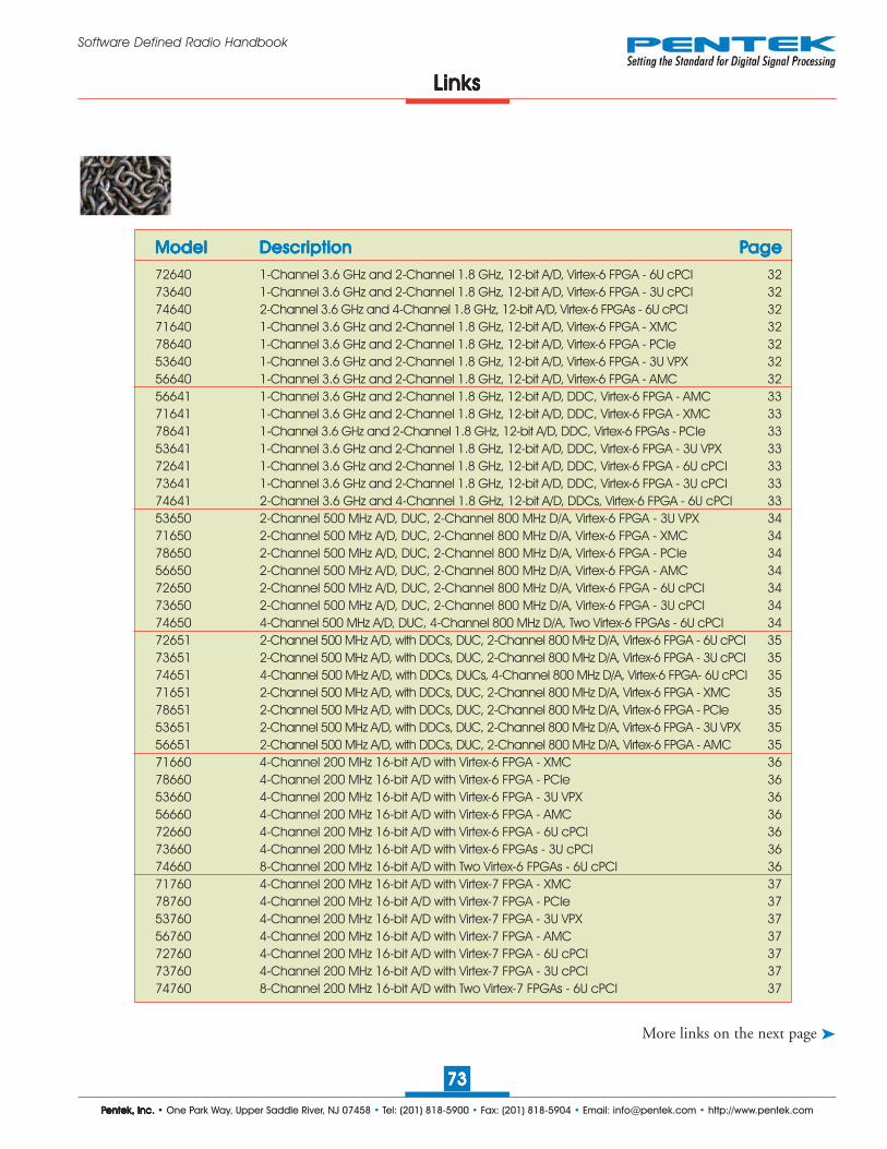
PPPPPentek, Inc.entek, Inc.entek, Inc.entek, Inc.entek, Inc. • One Park Way, Upper Saddle River, NJ 07458 • Tel: (201) 818-5900 • Fax: (201) 818-5904 • Email: [email protected] • http://www.pentek.com
7373737373
Software Defined Radio Handbook
ModelModelModelModelModel DescriptionDescriptionDescriptionDescriptionDescription PPPPPageageageageage72640 1-Channel 3.6 GHz and 2-Channel 1.8 GHz, 12-bit A/D, Virtex-6 FPGA - 6U cPCI 3273640 1-Channel 3.6 GHz and 2-Channel 1.8 GHz, 12-bit A/D, Virtex-6 FPGA - 3U cPCI 3274640 2-Channel 3.6 GHz and 4-Channel 1.8 GHz, 12-bit A/D, Virtex-6 FPGAs - 6U cPCI 3271640 1-Channel 3.6 GHz and 2-Channel 1.8 GHz, 12-bit A/D, Virtex-6 FPGA - XMC 3278640 1-Channel 3.6 GHz and 2-Channel 1.8 GHz, 12-bit A/D, Virtex-6 FPGA - PCIe 3253640 1-Channel 3.6 GHz and 2-Channel 1.8 GHz, 12-bit A/D, Virtex-6 FPGA - 3U VPX 3256640 1-Channel 3.6 GHz and 2-Channel 1.8 GHz, 12-bit A/D, Virtex-6 FPGA - AMC 3256641 1-Channel 3.6 GHz and 2-Channel 1.8 GHz, 12-bit A/D, DDC, Virtex-6 FPGA - AMC 3371641 1-Channel 3.6 GHz and 2-Channel 1.8 GHz, 12-bit A/D, DDC, Virtex-6 FPGA - XMC 3378641 1-Channel 3.6 GHz and 2-Channel 1.8 GHz, 12-bit A/D, DDC, Virtex-6 FPGAs - PCIe 3353641 1-Channel 3.6 GHz and 2-Channel 1.8 GHz, 12-bit A/D, DDC, Virtex-6 FPGA - 3U VPX 3372641 1-Channel 3.6 GHz and 2-Channel 1.8 GHz, 12-bit A/D, DDC, Virtex-6 FPGA - 6U cPCI 3373641 1-Channel 3.6 GHz and 2-Channel 1.8 GHz, 12-bit A/D, DDC, Virtex-6 FPGA - 3U cPCI 3374641 2-Channel 3.6 GHz and 4-Channel 1.8 GHz, 12-bit A/D, DDCs, Virtex-6 FPGA - 6U cPCI 3353650 2-Channel 500 MHz A/D, DUC, 2-Channel 800 MHz D/A, Virtex-6 FPGA - 3U VPX 3471650 2-Channel 500 MHz A/D, DUC, 2-Channel 800 MHz D/A, Virtex-6 FPGA - XMC 3478650 2-Channel 500 MHz A/D, DUC, 2-Channel 800 MHz D/A, Virtex-6 FPGA - PCIe 3456650 2-Channel 500 MHz A/D, DUC, 2-Channel 800 MHz D/A, Virtex-6 FPGA - AMC 3472650 2-Channel 500 MHz A/D, DUC, 2-Channel 800 MHz D/A, Virtex-6 FPGA - 6U cPCI 3473650 2-Channel 500 MHz A/D, DUC, 2-Channel 800 MHz D/A, Virtex-6 FPGA - 3U cPCI 3474650 4-Channel 500 MHz A/D, DUC, 4-Channel 800 MHz D/A, Two Virtex-6 FPGAs - 6U cPCI 3472651 2-Channel 500 MHz A/D, with DDCs, DUC, 2-Channel 800 MHz D/A, Virtex-6 FPGA - 6U cPCI 3573651 2-Channel 500 MHz A/D, with DDCs, DUC, 2-Channel 800 MHz D/A, Virtex-6 FPGA - 3U cPCI 3574651 4-Channel 500 MHz A/D, with DDCs, DUCs, 4-Channel 800 MHz D/A, Virtex-6 FPGA- 6U cPCI 3571651 2-Channel 500 MHz A/D, with DDCs, DUC, 2-Channel 800 MHz D/A, Virtex-6 FPGA - XMC 3578651 2-Channel 500 MHz A/D, with DDCs, DUC, 2-Channel 800 MHz D/A, Virtex-6 FPGA - PCIe 3553651 2-Channel 500 MHz A/D, with DDCs, DUC, 2-Channel 800 MHz D/A, Virtex-6 FPGA - 3U VPX 3556651 2-Channel 500 MHz A/D, with DDCs, DUC, 2-Channel 800 MHz D/A, Virtex-6 FPGA - AMC 3571660 4-Channel 200 MHz 16-bit A/D with Virtex-6 FPGA - XMC 3678660 4-Channel 200 MHz 16-bit A/D with Virtex-6 FPGA - PCIe 3653660 4-Channel 200 MHz 16-bit A/D with Virtex-6 FPGA - 3U VPX 3656660 4-Channel 200 MHz 16-bit A/D with Virtex-6 FPGA - AMC 3672660 4-Channel 200 MHz 16-bit A/D with Virtex-6 FPGA - 6U cPCI 3673660 4-Channel 200 MHz 16-bit A/D with Virtex-6 FPGAs - 3U cPCI 3674660 8-Channel 200 MHz 16-bit A/D with Two Virtex-6 FPGAs - 6U cPCI 3671760 4-Channel 200 MHz 16-bit A/D with Virtex-7 FPGA - XMC 3778760 4-Channel 200 MHz 16-bit A/D with Virtex-7 FPGA - PCIe 3753760 4-Channel 200 MHz 16-bit A/D with Virtex-7 FPGA - 3U VPX 3756760 4-Channel 200 MHz 16-bit A/D with Virtex-7 FPGA - AMC 3772760 4-Channel 200 MHz 16-bit A/D with Virtex-7 FPGA - 6U cPCI 3773760 4-Channel 200 MHz 16-bit A/D with Virtex-7 FPGA - 3U cPCI 3774760 8-Channel 200 MHz 16-bit A/D with Two Virtex-7 FPGAs - 6U cPCI 37
LinksLinksLinksLinksLinks
More links on the next page ➤

PPPPPentek, Inc.entek, Inc.entek, Inc.entek, Inc.entek, Inc. • One Park Way, Upper Saddle River, NJ 07458 • Tel: (201) 818-5900 • Fax: (201) 818-5904 • Email: [email protected] • http://www.pentek.com
7474747474
Software Defined Radio Handbook
LinksLinksLinksLinksLinks
ModelModelModelModelModel DescriptionDescriptionDescriptionDescriptionDescription PPPPPageageageageage
71661 4-Channel 200 MHz 16-bit A/D with Installed IP Cores - XMC 3878661 4-Channel 200 MHz 16-bit A/D with Installed IP Cores - PCIe 3853661 4-Channel 200 MHz 16-bit A/D with Installed IP Cores - 3U VPX 3856661 4-Channel 200 MHz 16-bit A/D with Installed IP Cores - AMC 3872661 4-Channel 200 MHz 16-bit A/D with Installed IP Cores - 6U cPCI 3873661 4-Channel 200 MHz 16-bit A/D with Installed IP Cores - 3U cPCI 3874661 8-Channel 200 MHz 16-bit A/D with Installed IP Cores - 6U cPCI 3878662 4-Channel 200 MHz 16-bit A/D with Installed IP Cores - PCIe 3971662 4-Channel 200 MHz 16-bit A/D with Installed IP Cores - XMC 3953662 4-Channel 200 MHz 16-bit A/D with Installed IP Cores - 3U VPX 3956662 4-Channel 200 MHz 16-bit A/D with Installed IP Cores - AMC 3972662 4-Channel 200 MHz 16-bit A/D with Installed IP Cores - 6U cPCI 3973662 4-Channel 200 MHz 16-bit A/D with Installed IP Cores - 3U cPCI 3974662 8-Channel 200 MHz 16-bit A/D with Installed IP Cores - 6U cPCI 3956670 4-Channel 1.25 GHz D/A with DUC, Virtex-6 FPGA - AMC 4071670 4-Channel 1.25 GHz D/A with DUC, Virtex-6 FPGA - XMC 4078670 4-Channel 1.25 GHz D/A with DUC, Virtex-6 FPGA - PCIe 4053670 4-Channel 1.25 GHz D/A with DUC, Virtex-6 FPGA - 3U VPX 4072670 4-Channel 1.25 GHz D/A with DUC, Virtex-6 FPGA - 6U cPCI 4073670 4-Channel 1.25 GHz D/A with DUC, Virtex-6 FPGA - 3U cPCI 4074670 8-Channel 1.25 GHz D/A with DUCs, and Two Virtex-6 FPGAs - 6U cPCI 4071671 4-Channel 1.25 GHz D/A with DUC, Extended Interpolation, Virtex-6 FPGA - XMC 4178671 4-Channel 1.25 GHz D/A with DUC, Extended Interpolation, Virtex-6 FPGA - PCIe 4153671 4-Channel 1.25 GHz D/A with DUC, Extended Interpolation, Virtex-6 FPGA - 3U VPX 4156671 4-Channel 1.25 GHz D/A with DUC, Extended Interpolation, Virtex-6 FPGA - AMC 4172671 4-Channel 1.25 GHz D/A with DUC, Extended Interpolation, Virtex-6 FPGA - 6U cPCI 4173671 4-Channel 1.25 GHz D/A with DUC, Extended Interpolation, Virtex-6 FPGA - 3U cPCI 4174671 8-Channel 1.25 GHz D/A with DUCs, Ext. Interpolation, Two Virtex-6 FPGAs - 6U cPCI 4153690 L-Band RF Tuner with 2-Channel 200 MHz A/D and Virtex-6 FPGA - 3U VPX 4271690 L-Band RF Tuner with 2-Channel 200 MHz A/D and Virtex-6 FPGA - XMC 4278690 L-Band RF Tuner with 2-Channel 200 MHz A/D and Virtex-6 FPGA - PCIe 4256690 L-Band RF Tuner with 2-Channel 200 MHz A/D and Virtex-6 FPGA - AMC 4272690 L-Band RF Tuner with 2-Channel 200 MHz A/D and Virtex-6 FPGA - 6U cPCI 4273690 L-Band RF Tuner with 2-Channel 200 MHz A/D and Virtex-6 FPGA - 3U cPCI 4274690 Dual L-Band RF Tuner with 4-Channel 200 MHz A/D and Two Virtex-6 FPGAs - 6U cPCI 426890 2.2 GHz Clock, Sync and Gate Distribution Board - VME 436891 System Synchronizer and Distribution Board - VME 447190 Multifrequency Clock Synthesizer - PMC 457290 Multifrequency Clock Synthesizer - 6U cPCI 457390 Multifrequency Clock Synthesizer - 3U cPCI 457690 Multifrequency Clock Synthesizer - PCI 457790 Multifrequency Clock Synthesizer - Full-length PCIe 457890 Multifrequency Clock Synthesizer - Half-length PCIe 455390 Multifrequency Clock Synthesizer - 3U VPX 45
More links on the next page ➤

PPPPPentek, Inc.entek, Inc.entek, Inc.entek, Inc.entek, Inc. • One Park Way, Upper Saddle River, NJ 07458 • Tel: (201) 818-5900 • Fax: (201) 818-5904 • Email: [email protected] • http://www.pentek.com
7575757575
Software Defined Radio Handbook
LinksLinksLinksLinksLinks
Click here Putting FPGAs to Work in Software Radio Systems HandbookClick here Critical Techniques for High-Speed A/D Converters in Real-Time Systems HandbookClick here High-Speed Switched Serial Fabrics Improve System Design HandbookClick here High-Speed, Real-Time Recording Systems HandbookClick here Onyx Virtex-7 and Cobalt Virtex-6 Product CatalogClick here Pentek Product Catalog
ModelModelModelModelModel DescriptionDescriptionDescriptionDescriptionDescription PPPPPageageageageage
7191 Programmable Multifrequency Clock Synthesizer - PMC 467291 Programmable Multifrequency Clock Synthesizer - 6U cPCI 467391 Programmable Multifrequency Clock Synthesizer - 3U cPCI 467691 Programmable Multifrequency Clock Synthesizer - PCI 467791 Programmable Multifrequency Clock Synthesizer - Full-length PCIe 467891 Programmable Multifrequency Clock Synthesizer - Half-length PCIe 465391 Programmable Multifrequency Clock Synthesizer - 3U VPX 467192 High-Speed Synchronizer and Distribution Board - PMC/XMC 477892 High-Speed Synchronizer and Distribution Board - PCIe 475392 High-Speed Synchronizer and Distribution Board - 3U VPX 477292 High-Speed Synchronizer and Distribution Board - 6U cPCI 477392 High-Speed Synchronizer and Distribution Board - 3U cPCI 477492 High-Speed Synchronizer and Distribution Board - 6U cPCI 477893 System Synchronizer and Distribution Board - PCIe 489190 Clock and Sync Generator for I/O Modules - Rackmount 499192 High-Speed System Synchronizer Unit - Rackmount 50RTS 2706 Eight-Channel RF/IF 200 MS/sec Rackmount Recorder 51RTS 2707 Four-Channel RF/IF 500 MS/sec Rackmount Recorder 52RTS 2709 Ultra Wideband One- or Two-Channel RF/IF, 3.2 GS/sec Rackmount Recorder 53RTS 2715 Two-Channel 10 Gigabit Ethernet Rackmount Recorder 54RTS 2716 Eight-Channel Serial FPDP Rackmount Recorder 55RTR 2726 Four-Channel RF/IF 200 MS/sec Rugged Portable Recorder 56RTR 2727 Two-Channel RF/IF 500 MS/sec Rugged Portable Recorder 57RTR 2736 Eight-Channel Serial FPDP Rugged Portable Recorder 58RTR 2746 Eight-Channel RF/IF 200 MS/sec Rugged Rackmount Recorder 59RTR 2747 Four-Channel RF/IF 500 MS/sec Rugged Rackmount Recorder 60RTR 2749 Ultra Wideband One- or Two-Channel RF/IF, 3.2 GS/sec Rugged Rackmount Recorder 61RTR 2755 Two-Channel 10 Gigabit Ethernet Rugged Rackmount Recorder 62RTR 2756 Eight-Channel Serial FPDP Rugged Rackmount Recorder 63RTX 2786 Four-Channel RF/IF 200 MS/sec Extreme 3U VPX Recorder 64
Handbooks and CatalogsHandbooks and CatalogsHandbooks and CatalogsHandbooks and CatalogsHandbooks and Catalogs