solar cells. the electrical conductivity of semiconductors conductivity increases as t decreases....
TRANSCRIPT
Solar Cells
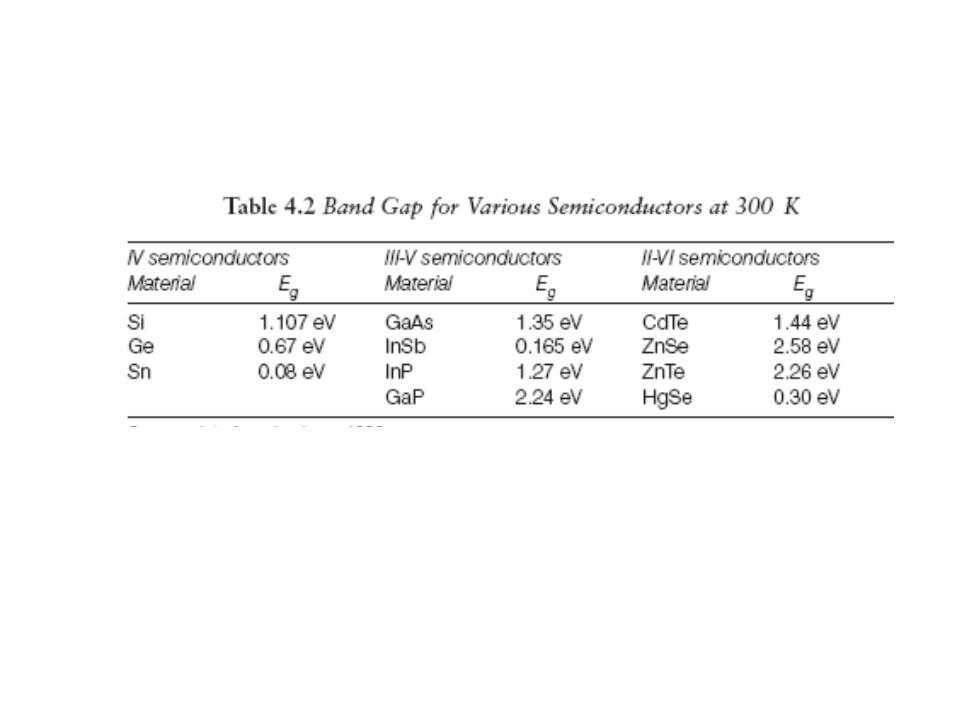
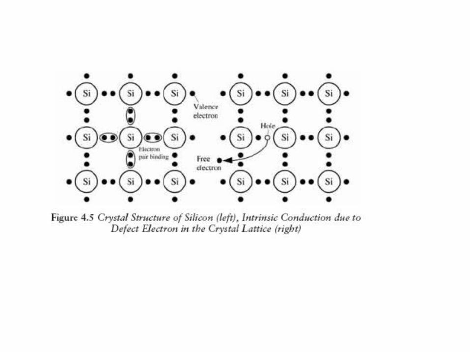
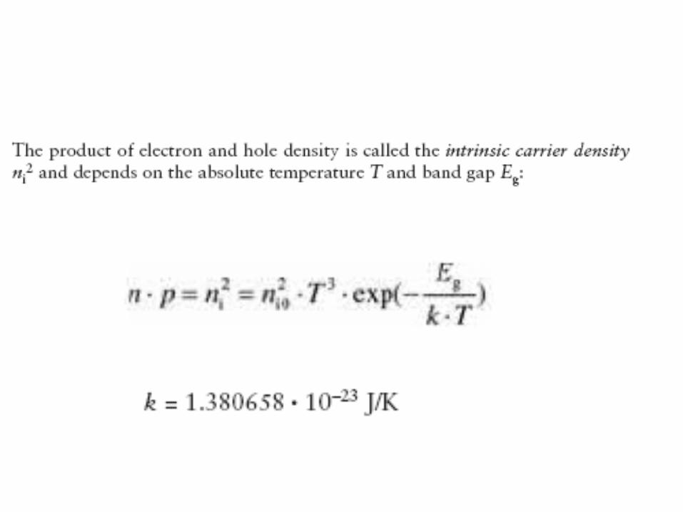
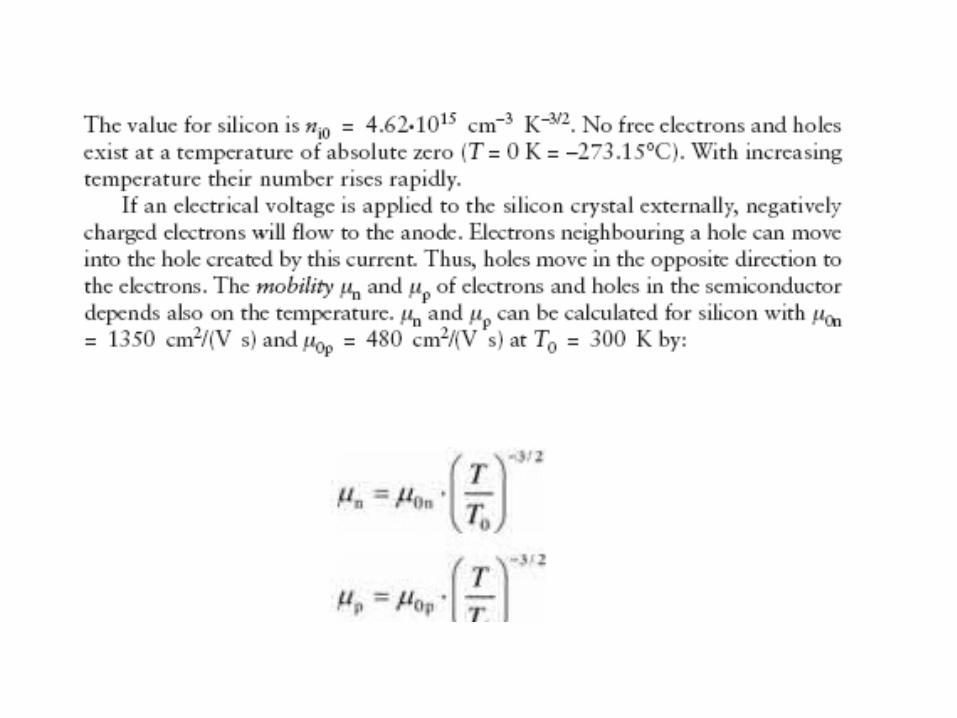
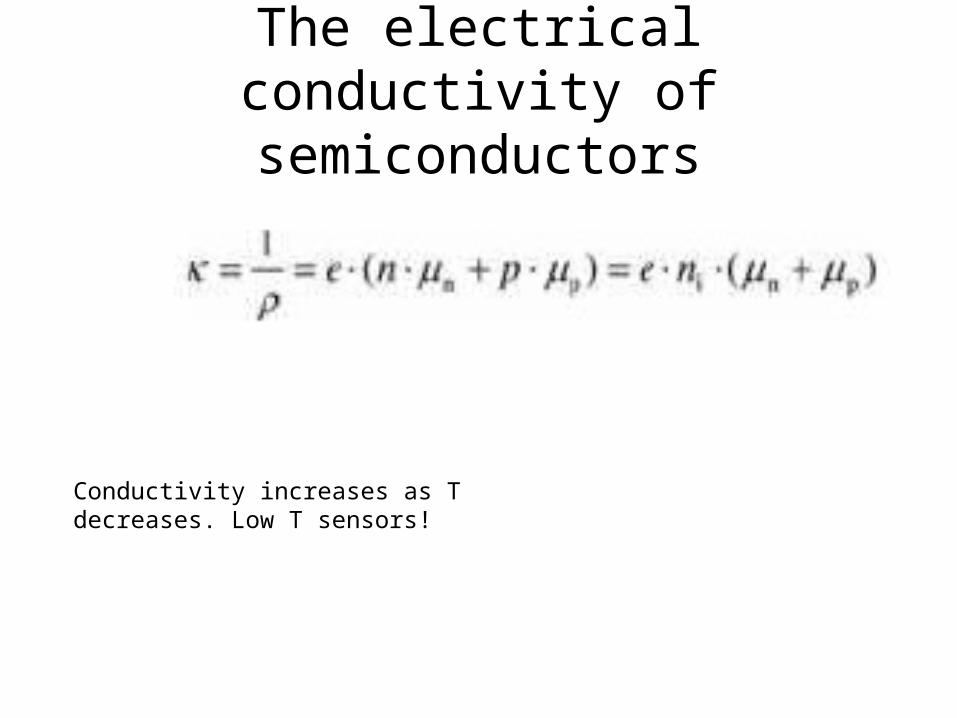
The electrical conductivity of semiconductors
Conductivity increases as T decreases. Low T sensors!
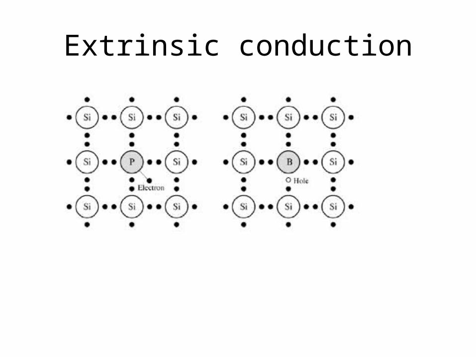
Extrinsic conduction
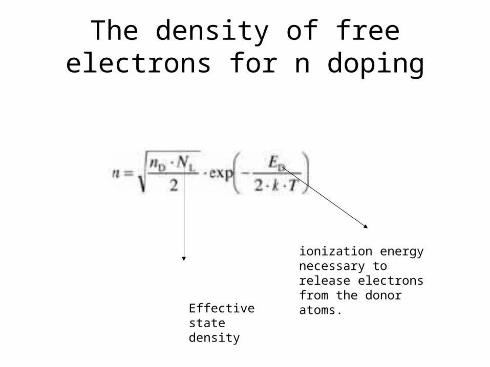
The density of free electrons for n doping
Effective state density
ionization energy necessary to release electronsfrom the donor atoms.
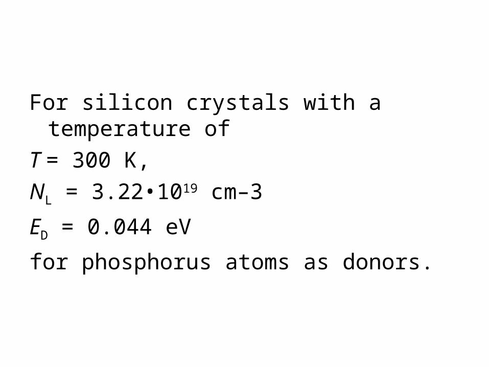
For silicon crystals with a temperature of
T = 300 K,
NL = 3.22•1019 cm–3
ED = 0.044 eV
for phosphorus atoms as donors.
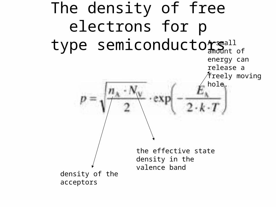
The density of free electrons for ptype semiconductors
density of the acceptors
the effective state density in thevalence band
A small amount of energy can release a freely moving hole.
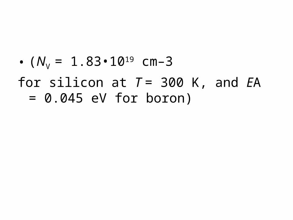
• (NV = 1.83•1019 cm–3
for silicon at T = 300 K, and EA = 0.045 eV for boron)

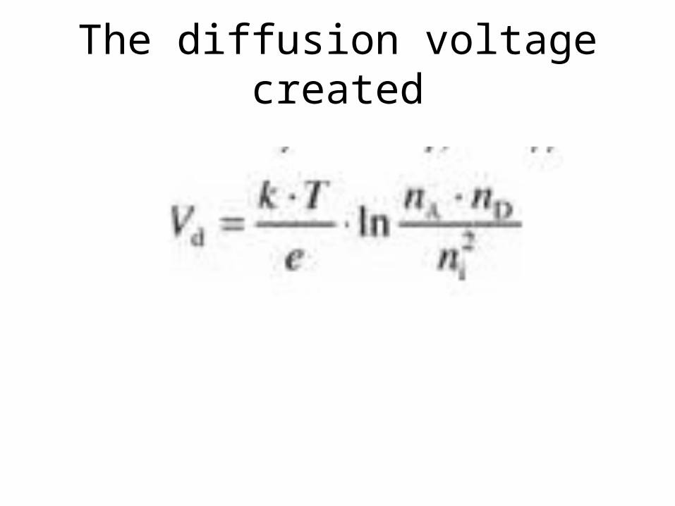
The diffusion voltage created
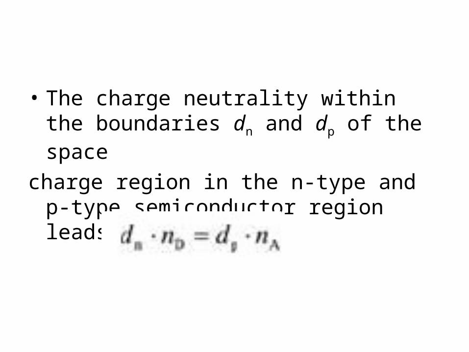
• The charge neutrality within the boundaries dn and dp of the space
charge region in the n-type and p-type semiconductor region leads to:
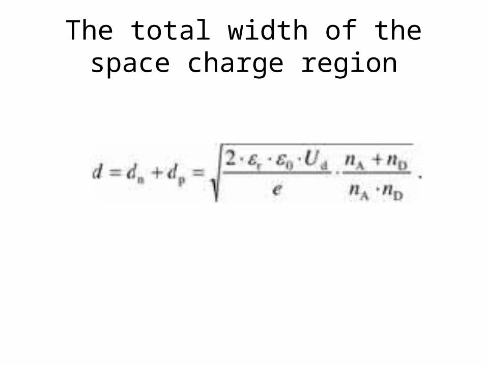
The total width of the space charge region
• When electrons are lifted from the valence band into the conduction band and thus released from the atom in the space charge region, the electric field will pull them into the n-region.
• Similarly, generated holes will move into the p-region. This can be explained in the energy band model by band bending in the space charge region.
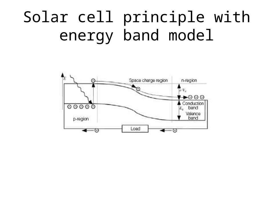
Solar cell principle with energy band model
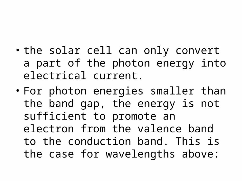
• the solar cell can only convert a part of the photon energy into electrical current.
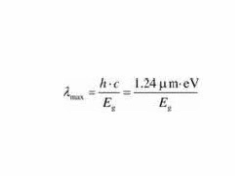
• For photon energies smaller than the band gap, the energy is not sufficient to promote an electron from the valence band to the conduction band. This is the case for wavelengths above:
• Not all the energy of photons with wavelengths near the band gap is converted to electricity.
• The solar cell surface reflects a part of the incoming light, and some is transmitted through the solar cell.
• Furthermore, electrons can recombine with holes. In other words, they can fall back to the valence band before they are converted to electricity.
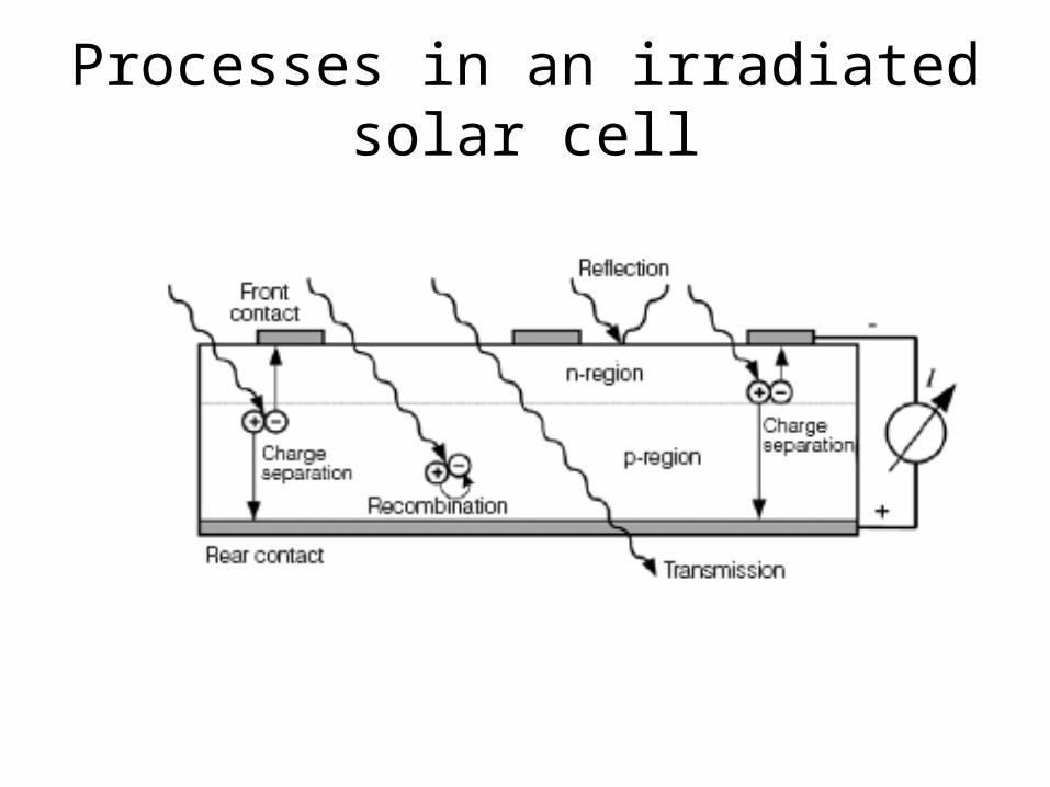
Processes in an irradiated solar cell
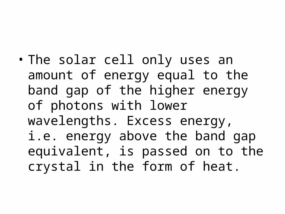
• The solar cell only uses an amount of energy equal to the band gap of the higher energy of photons with lower wavelengths. Excess energy, i.e. energy above the band gap equivalent, is passed on to the crystal in the form of heat.
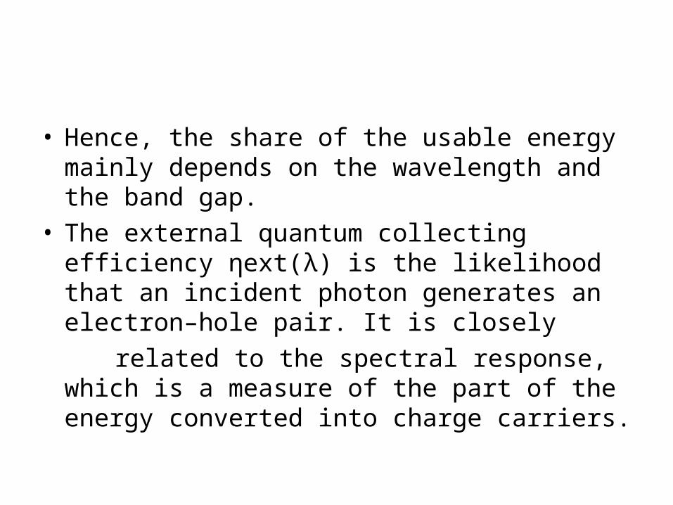
• Hence, the share of the usable energy mainly depends on the wavelength and the band gap.
• The external quantum collecting efficiency ηext(λ) is the likelihood that an incident photon generates an electron–hole pair. It is closely
related to the spectral response, which is a measure of the part of the energy converted into charge carriers.

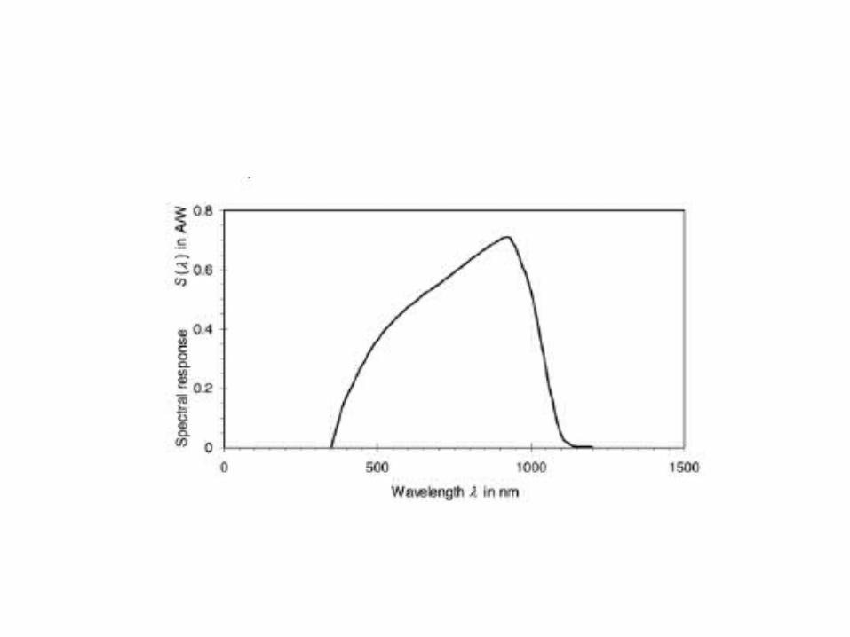
Spectral response
external quantum collecting efficiency
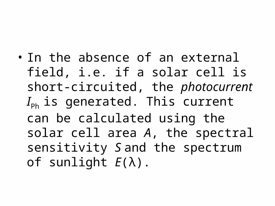
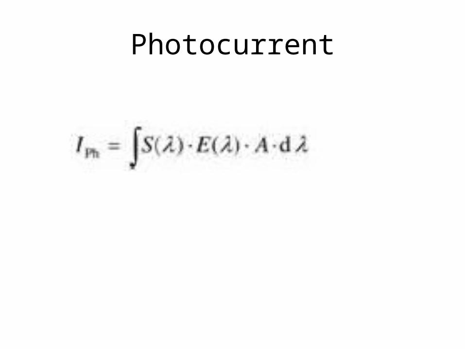
• In the absence of an external field, i.e. if a solar cell is short-circuited, the photocurrent IPh is generated. This current can be calculated using the solar cell area A, the spectral sensitivity S and the spectrum of sunlight E(λ).
Photocurrent
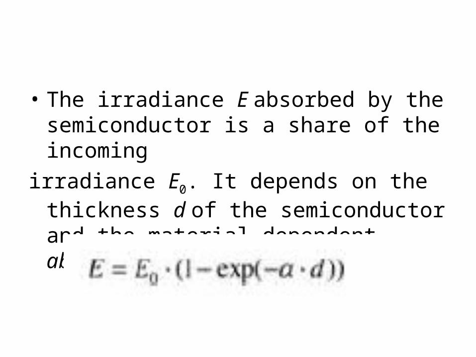
• The irradiance E absorbed by the semiconductor is a share of the incoming
irradiance E0. It depends on the thickness d of the semiconductor and the material-dependent absorption coefficient α:
Comparison of semiconductors
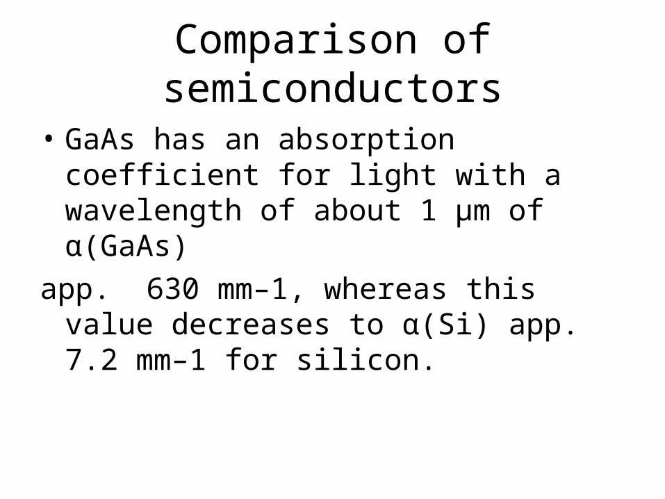
• GaAs has an absorption coefficient for light with a wavelength of about 1 μm of α(GaAs)
app. 630 mm–1, whereas this value decreases to α(Si) app. 7.2 mm–1 for silicon.
• For both semiconductors to absorb the same amount of light, the silicon will
have to be 87.5 times thicker than a GaAs semiconductor.
The wavelength dependence of the absorption coefficients must be considered for an exact calculation.
Crystalline silicon solar cells should have a thickness of at least about 200 μm for high absorptions.
PRODUCTION OF SOLAR CELLS AND SOLAR MODULES
• Crystalline silicon solar cells
Various semiconductor materials are suited to solar cell production; however,
silicon is the most commonly used material today.
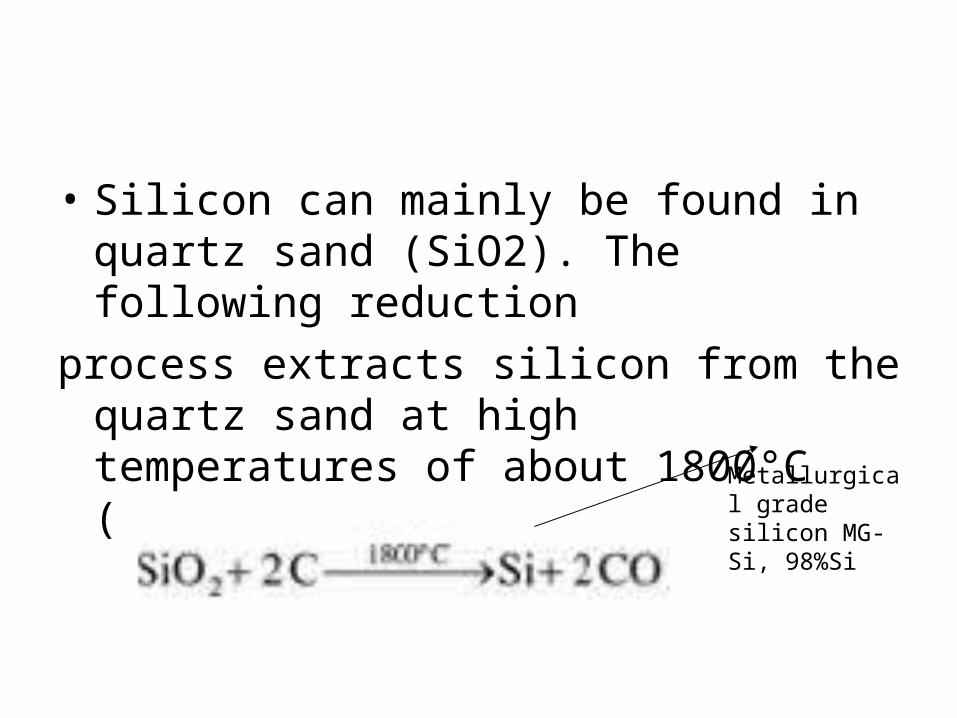
• Silicon can mainly be found in quartz sand (SiO2). The following reduction
process extracts silicon from the quartz sand at high temperatures of about 1800°C (3272°F):
Metallurgical grade silicon MG-Si, 98%Si
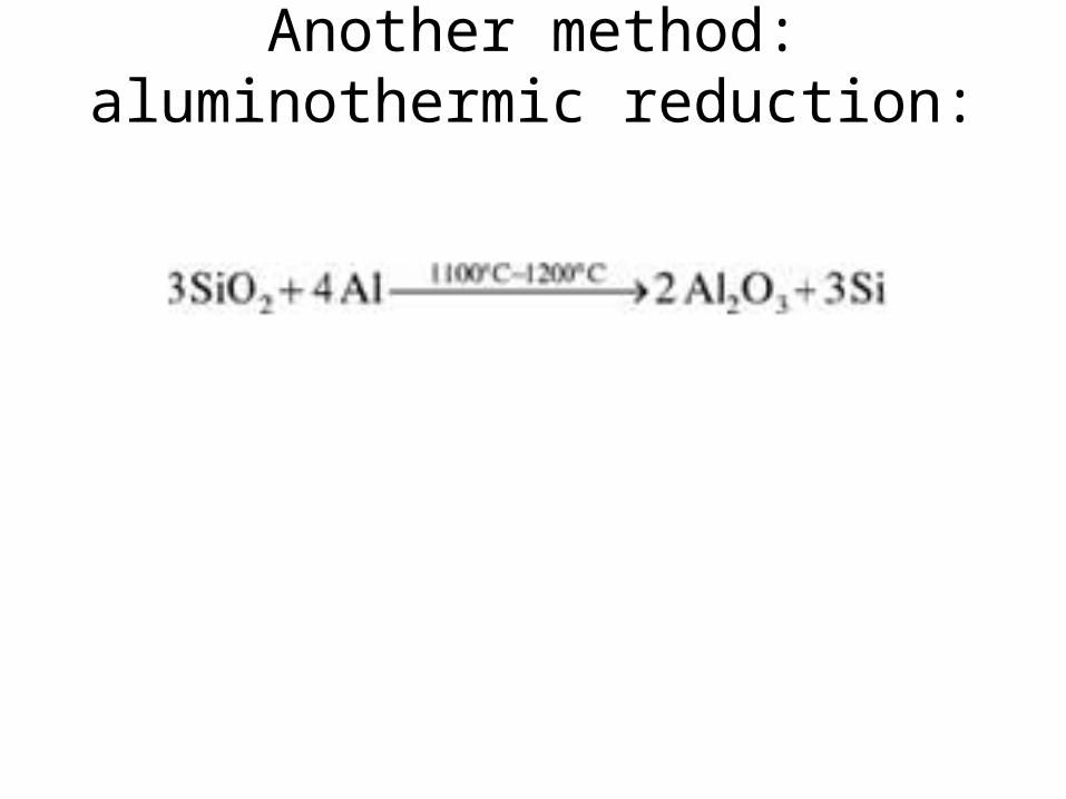
Another method: aluminothermic reduction:
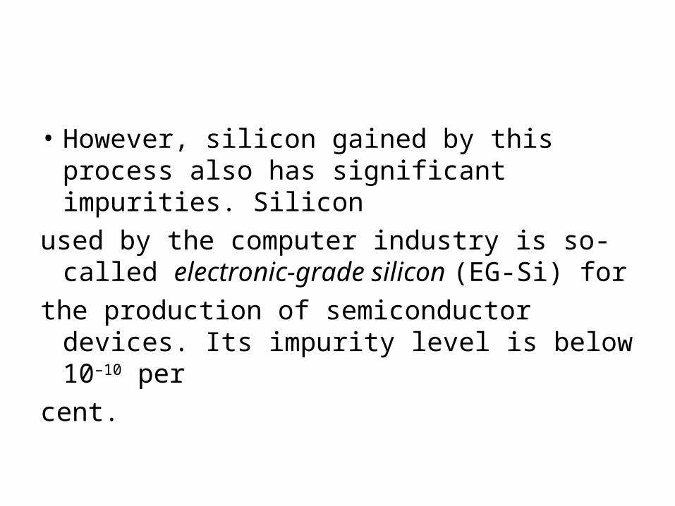
• However, silicon gained by this process also has significant impurities. Silicon
used by the computer industry is so-called electronic-grade silicon (EG-Si) for
the production of semiconductor devices. Its impurity level is below 10–10 per
cent.
SOG-Si
• This high purity is not necessary for solar cell production, in which solargrade
silicon (SOG-Si) is commonly used. Nevertheless, purification processes
are needed for the production of SOG-Si.
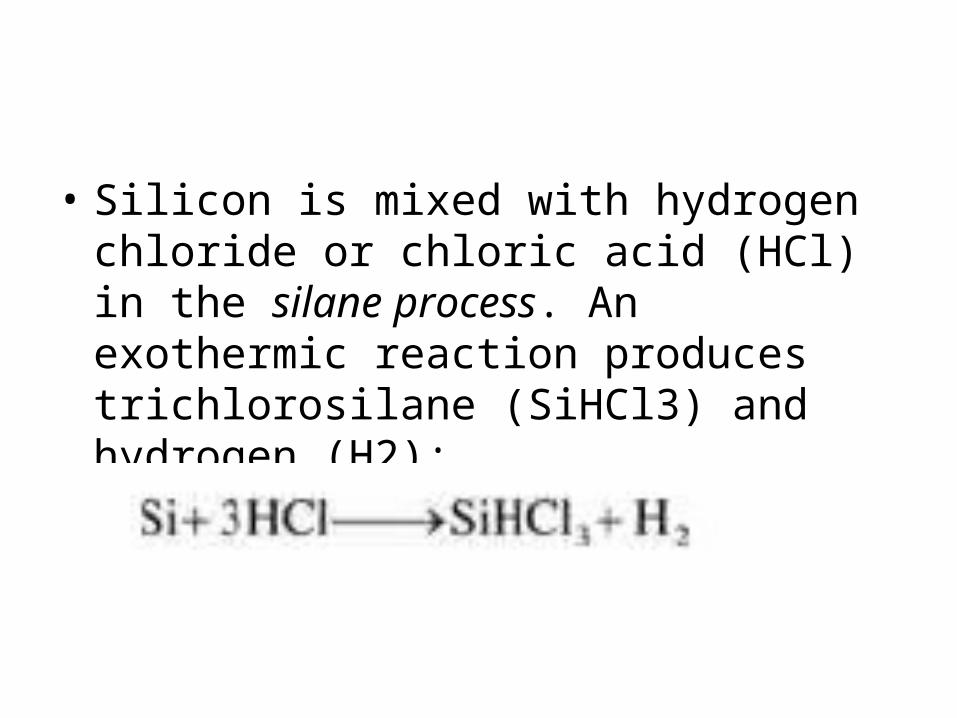
• Silicon is mixed with hydrogen chloride or chloric acid (HCl) in the silane process. An exothermic reaction produces trichlorosilane (SiHCl3) and hydrogen (H2):
• Trichlorosilane is liquid at temperatures of 30°C. Multiple fraction distillations are used to remove the impurities. The chemical vapour deposition (CVD) process is used for silicon recovery.
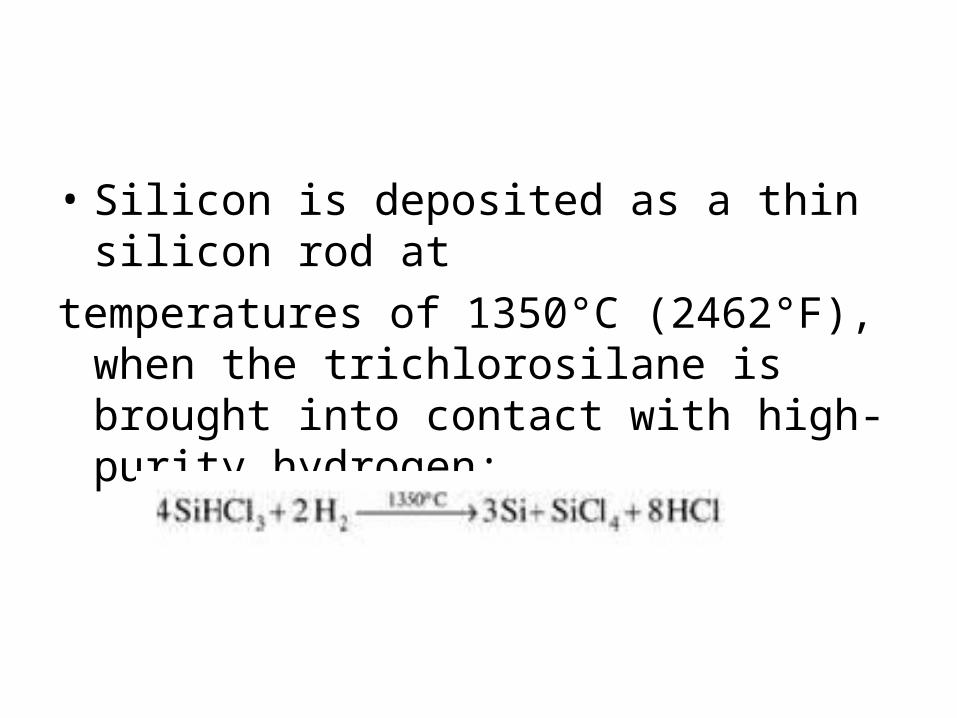
• Silicon is deposited as a thin silicon rod at
temperatures of 1350°C (2462°F), when the trichlorosilane is brought into contact with high-purity hydrogen:
• The end product is a high-purity silicon rod with diameters of up to 30 cm (about 12 inches) and lengths up to 2 m (about 80 inches). These rods can be used for the production of polycrystalline solar cells, which consist of a number of crystals, rather than a single crystal. The crystals of polycrystalline silicon are differently oriented and separated by grain boundaries. They introduce some efficiency losses.
• To increase solar cell efficiency, monocrystalline material can be produced from polycrystalline material applying the Czochralski or float zone process.
• Seeding a single crystal at high temperatures transforms the polycrystalline silicon to the desired monocrystalline silicon. No grain boundaries are present in the resulting material and thus losses within a solar cell are reduced.
• The silicon slices, or so-called wafers, are cleaned and doped in the following steps.
• Hydrofluoric acid removes any saw damage. Phosphorus and boron are used for doping silicon to create the p-n junction.
• Gaseous dopants are mixed with a carrier gas such as nitrogen (N2) or oxygen (O2) for gas diffusion, and this gas mixture flows over the silicon wafers. The impurity atoms diffuse into the silicon wafer depending on the gas mixture, temperature and flow velocity. Etching cleans the surface of the doped semiconductor.
• Finally, cell contacts are added. A screen printing process adds the front and rear contacts. Materials for the contacts are metals or alloys of aluminium or silver. The rear contact usually covers the whole cell area. Thin contact fingers are used for the front contacts, because they obstruct and reflect sunlight. Only a minimum of the cell’s surface should be covered by contacts in order to optimize light capture.
• Finally, an antireflective coating is added to the solar cell. This coating reduces reflection at the metallic silicon surface. Titanium dioxide (TiO2) is mostly used for the coating and gives the solar cell its typical blue colour.
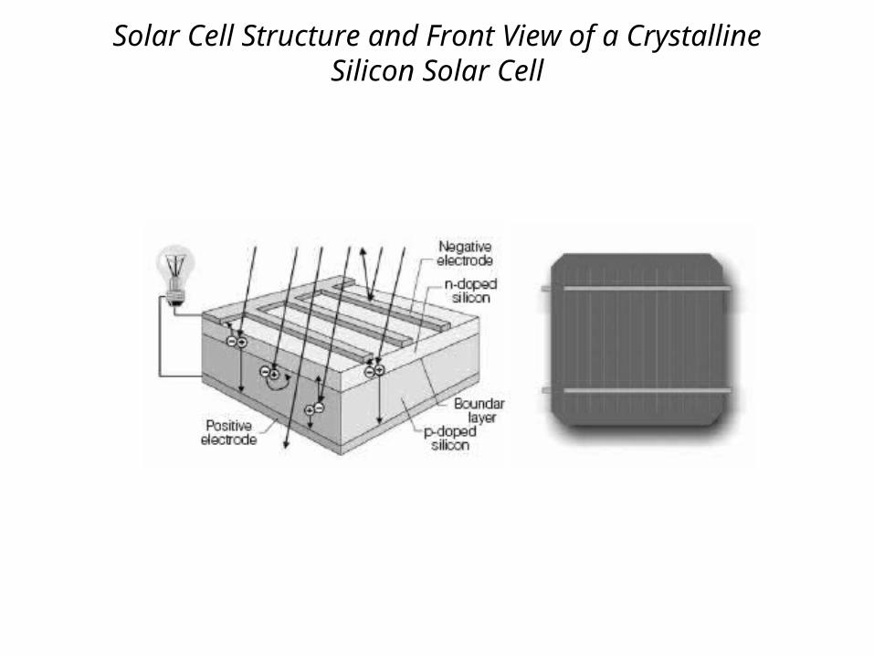
Solar Cell Structure and Front View of a CrystallineSilicon Solar Cell
Module sizes
• To avoid climatic damage several solar cells with an edge length between 10 and 21 cm are combined in a solar module for cell protection. Many modules are made up of 32–40 cells; however, other module sizes with significantly more or fewer cells exist.
Thin film modules
• Besides crystalline silicon, thin film modules hold promise for the cells of the
future.
They can be made of amorphous silicon and other materials such as cadmium telluride (CdTe) or copper indium diselenide (CuInSe2 or CIS).
• Thin film modules can be produced using a fraction of the semiconductor material
necessary for crystalline modules and this promises lower production costs in
the medium term.
ELECTRICAL DESCRIPTION OF SOLAR CELLS
• Simple equivalent circuit• A photovoltaic solar cell is a large area
diode. It consists of an n-type and ptypedoped semiconductor with a resulting space
charge layer. Typically, a non-irradiated solar cell has
nearly the same behaviour as a diode. Therefore,a simple diode can describe the equivalent circuit.
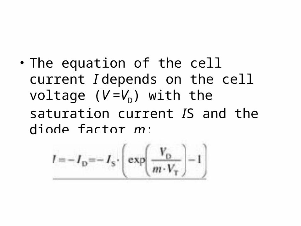
• The equation of the cell current I depends on the cell voltage (V =VD) with the saturation current IS and the diode factor m:
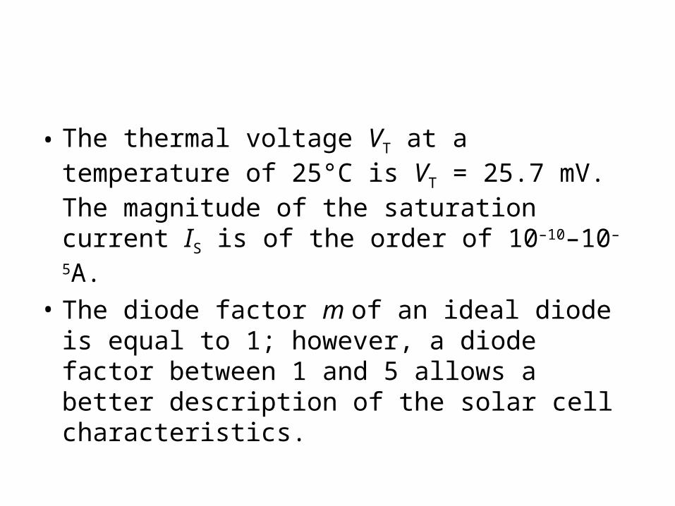
• The thermal voltage VT at a temperature of 25°C is VT = 25.7 mV. The magnitude of the saturation current IS is of the order of 10–10–10–5A.
• The diode factor m of an ideal diode is equal to 1; however, a diode factor between 1 and 5 allows a better description of the solar cell characteristics.
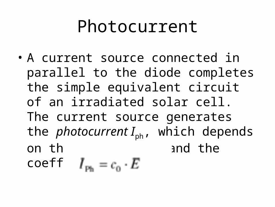
Photocurrent
• A current source connected in parallel to the diode completes the simple equivalent circuit of an irradiated solar cell. The current source generates the photocurrent Iph, which depends on the irradiance E and the coefficient c0:
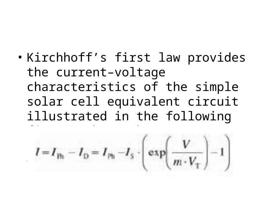
• Kirchhoff’s first law provides the current–voltage characteristics of the simple solar cell equivalent circuit illustrated in the following figures shows the characteristic curves at different irradiances):
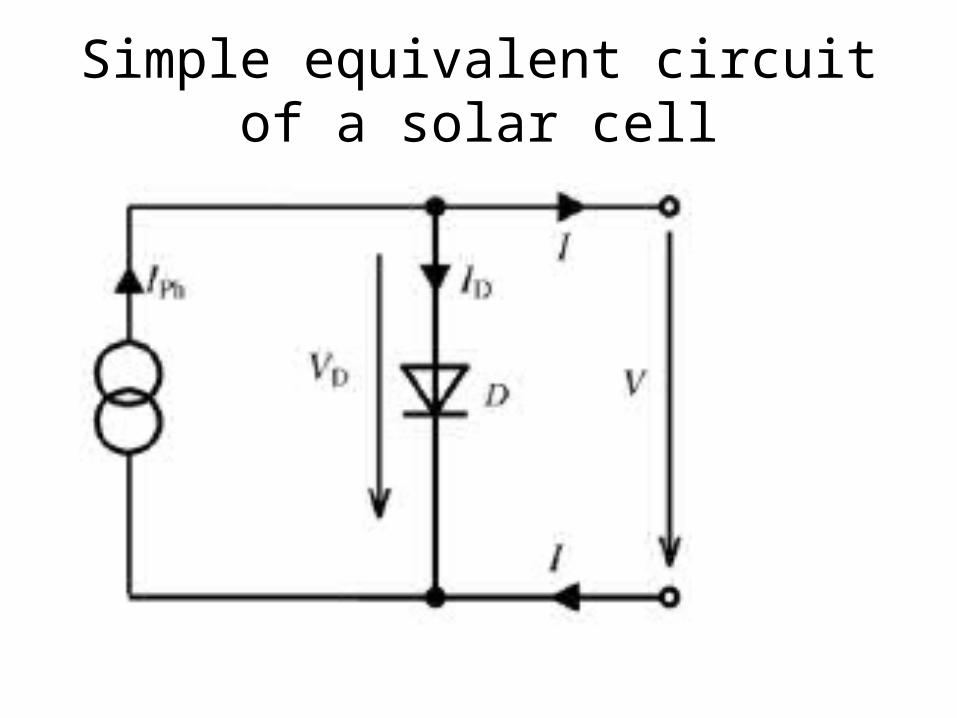
Simple equivalent circuit of a solar cell
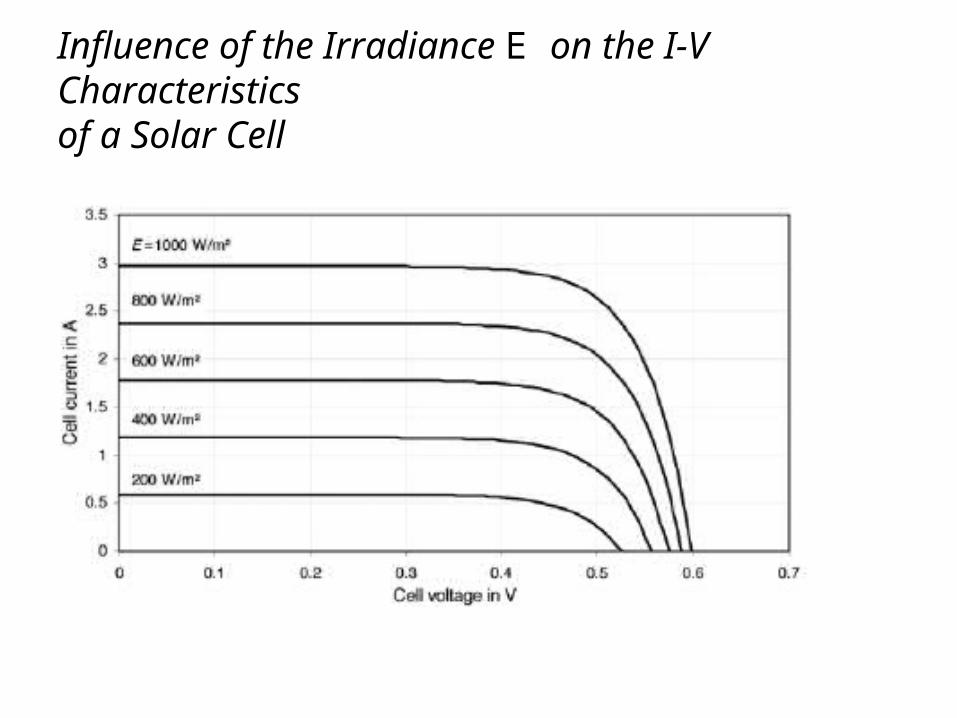
Influence of the Irradiance E on the I-V Characteristicsof a Solar Cell
Extended equivalent circuit
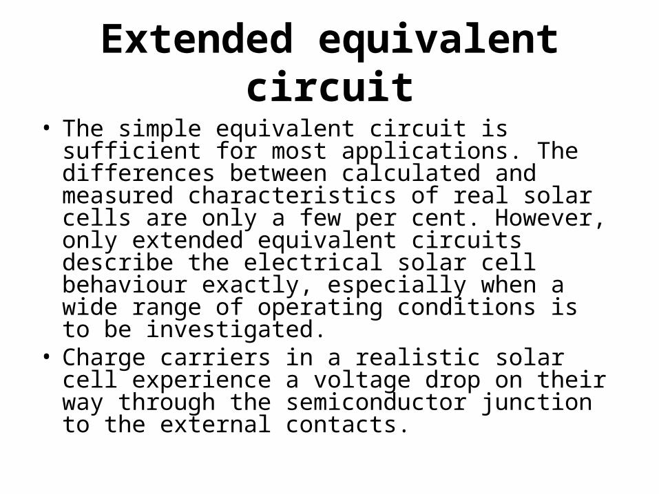
• The simple equivalent circuit is sufficient for most applications. The differences between calculated and measured characteristics of real solar cells are only a few per cent. However, only extended equivalent circuits describe the electrical solar cell behaviour exactly, especially when a wide range of operating conditions is to be investigated.
• Charge carriers in a realistic solar cell experience a voltage drop on their way through the semiconductor junction to the external contacts.
• A series resistance RS expresses this voltage drop. An additional parallel resistance RP describes the leakage currents at the cell edges.
The following figure shows the modified equivalent circuit including both resistances.
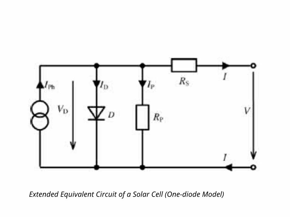
Extended Equivalent Circuit of a Solar Cell (One-diode Model)
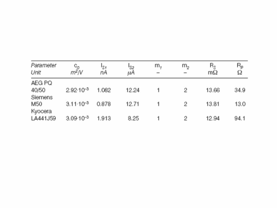
• The series resistance RS of real cells is in the range of several milliohms (mΩ), the parallel resistance RP is usually higher than 10 Ω.
• The following figures illustrate the influence of both resistances in terms of the I-V characteristics.
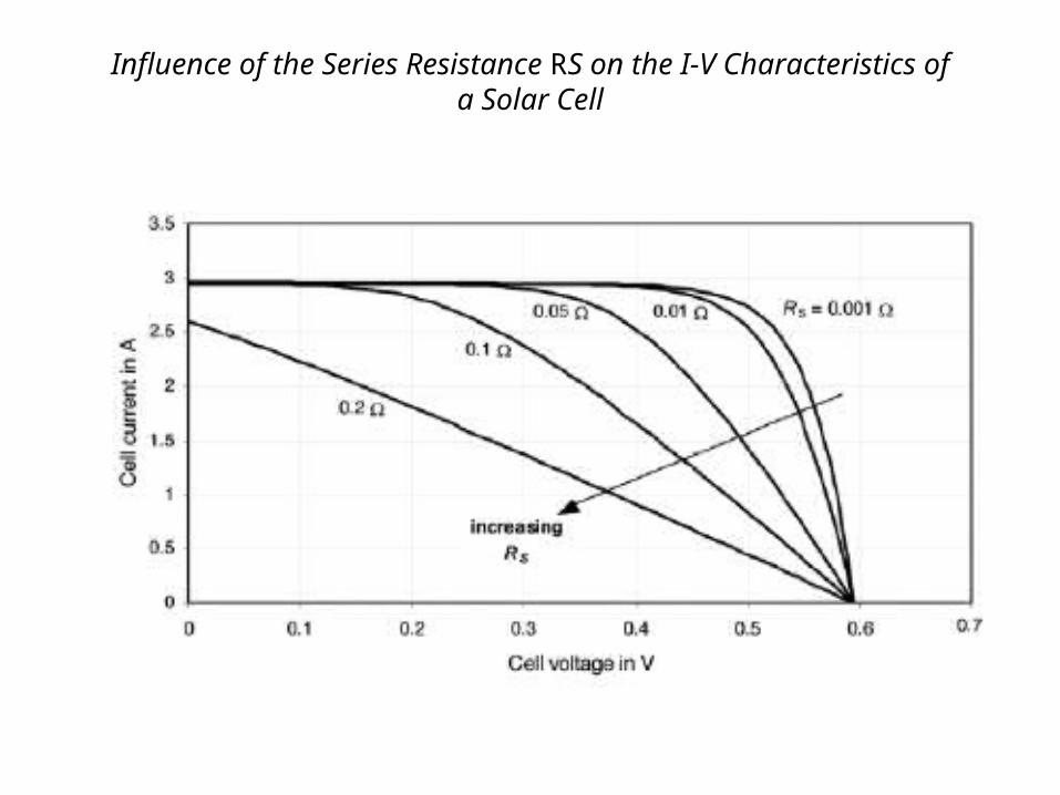
Influence of the Series Resistance RS on the I-V Characteristics ofa Solar Cell
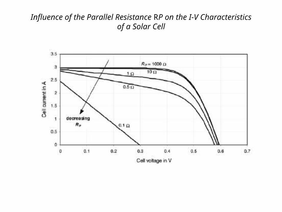
Influence of the Parallel Resistance RP on the I-V Characteristicsof a Solar Cell
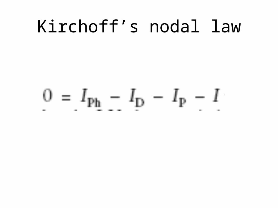
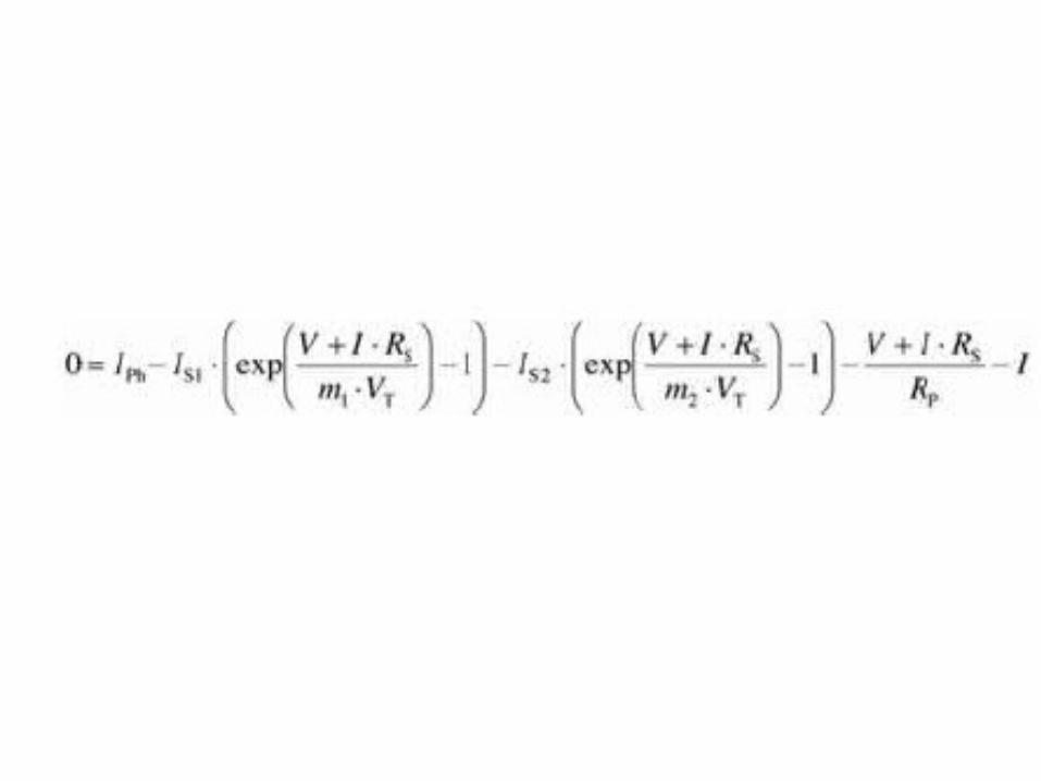
Kirchoff’s nodal law
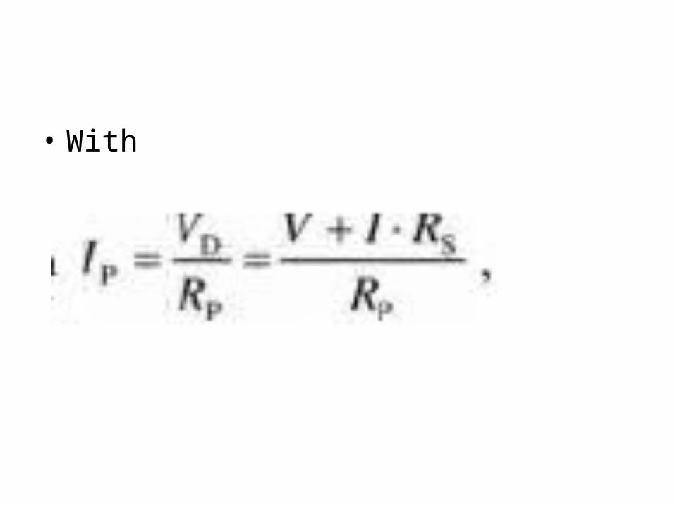
• With
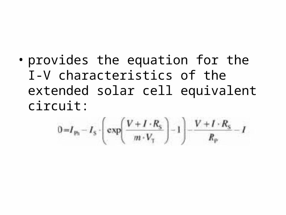
• provides the equation for the I-V characteristics of the extended solar cell equivalent circuit:
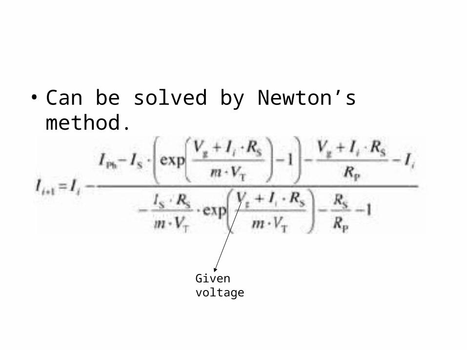
• Can be solved by Newton’s method.
Given voltage
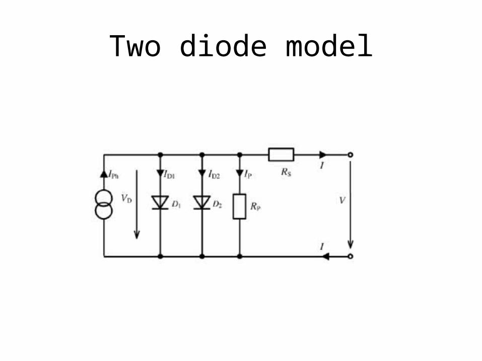
Two diode model
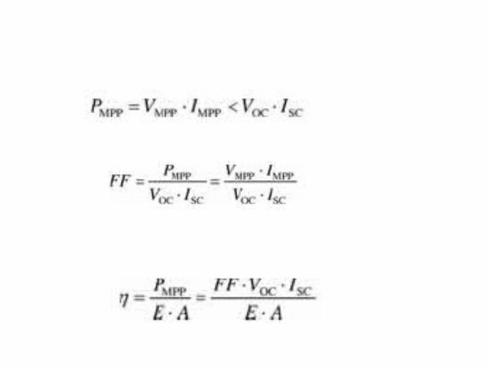
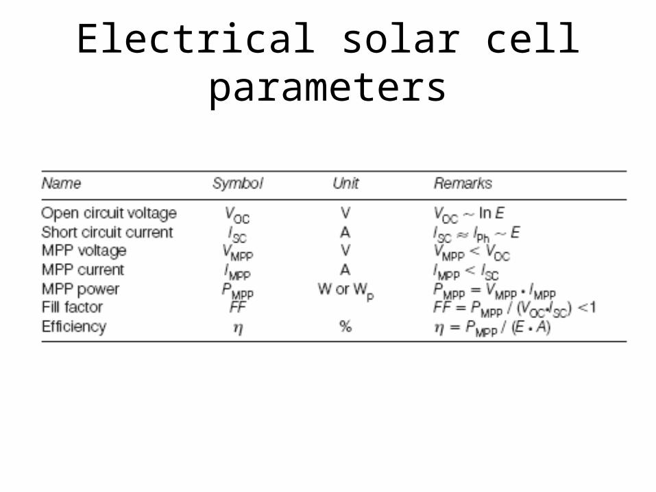
Further electrical solar cell parameters
• The voltage of a short-circuited solar cell is equal to zero, in which case, the short circuit current ISC is approximately equal to the photocurrent IPh.
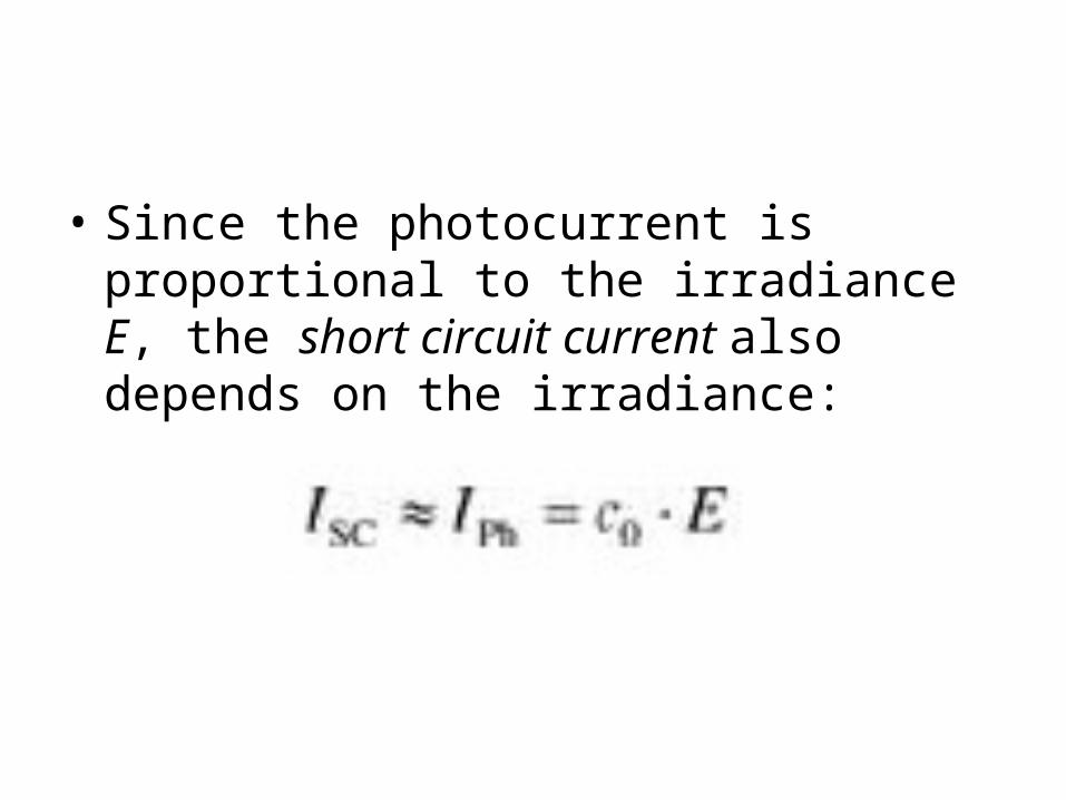
• Since the photocurrent is proportional to the irradiance E, the short circuit current also depends on the irradiance:
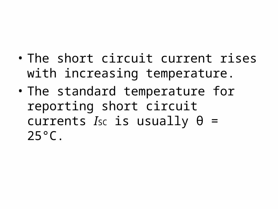
• The short circuit current rises with increasing temperature.
• The standard temperature for reporting short circuit currents ISC is usually ϑ = 25°C.
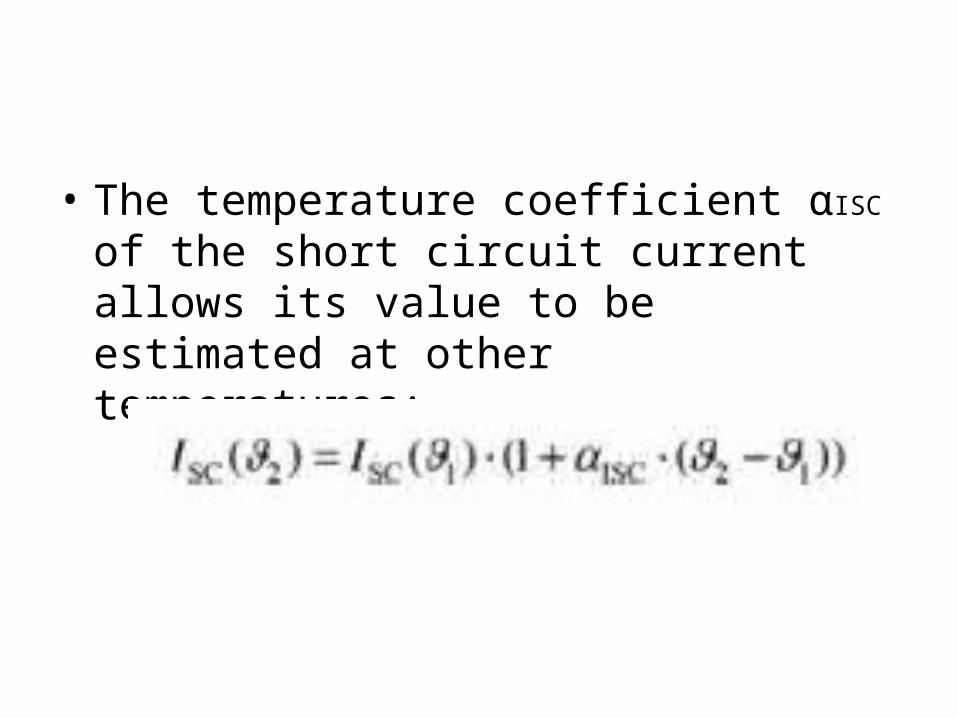
• The temperature coefficient αISC of the short circuit current allows its value to be estimated at other temperatures:
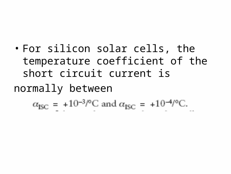
• For silicon solar cells, the temperature coefficient of the short circuit current is
normally between
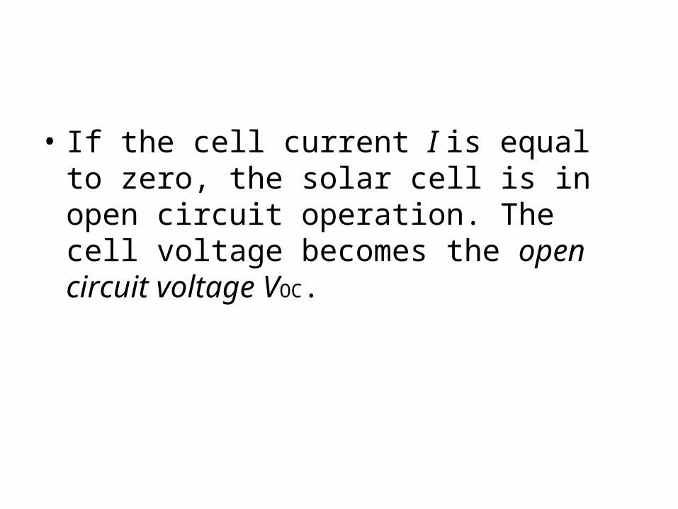
• If the cell current I is equal to zero, the solar cell is in open circuit operation. The cell voltage becomes the open circuit voltage VOC.
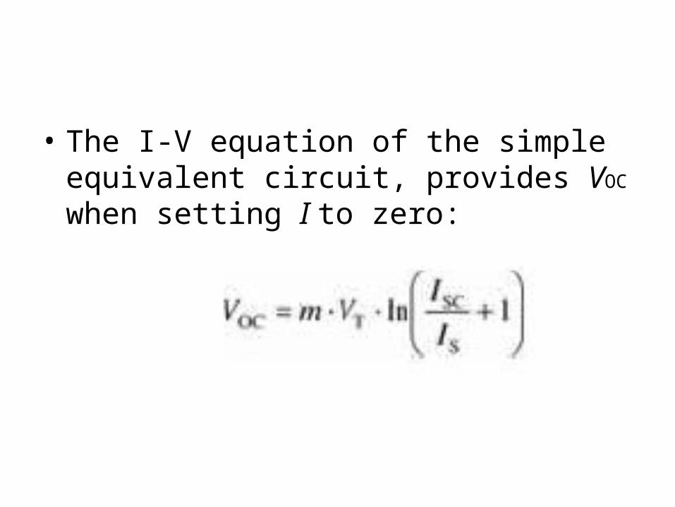
• The I-V equation of the simple equivalent circuit, provides VOC when setting I to zero:
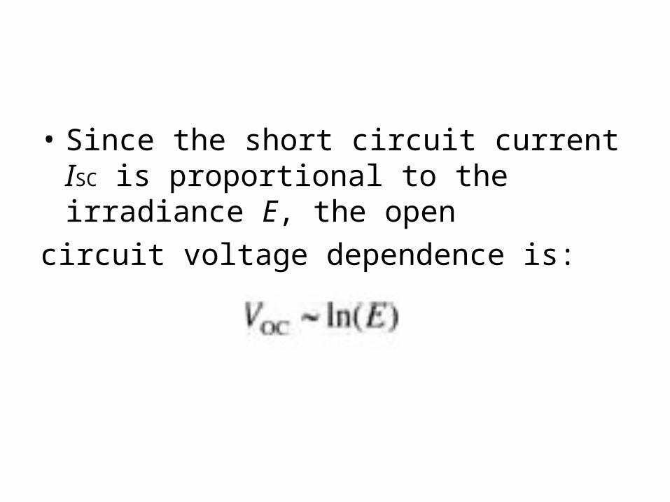
• Since the short circuit current ISC is proportional to the irradiance E, the open
circuit voltage dependence is:
• The temperature coefficient αVOC of the open circuit voltage is obtained similarly to the short circuit current. It commonly has a negative sign. For silicon solar cells, the temperature coefficient is between
• αVOC = –3•10–3/°C and αVOC = –5 • 10–3/°C.
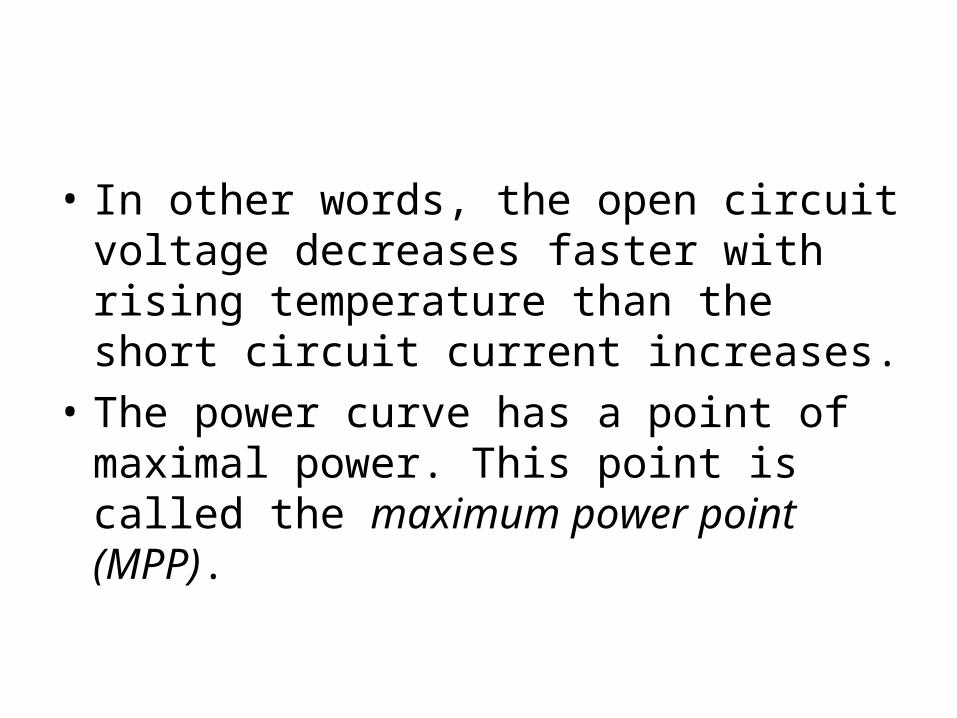
• In other words, the open circuit voltage decreases faster with rising temperature than the short circuit current increases.
• The power curve has a point of maximal power. This point is called the maximum power point (MPP).
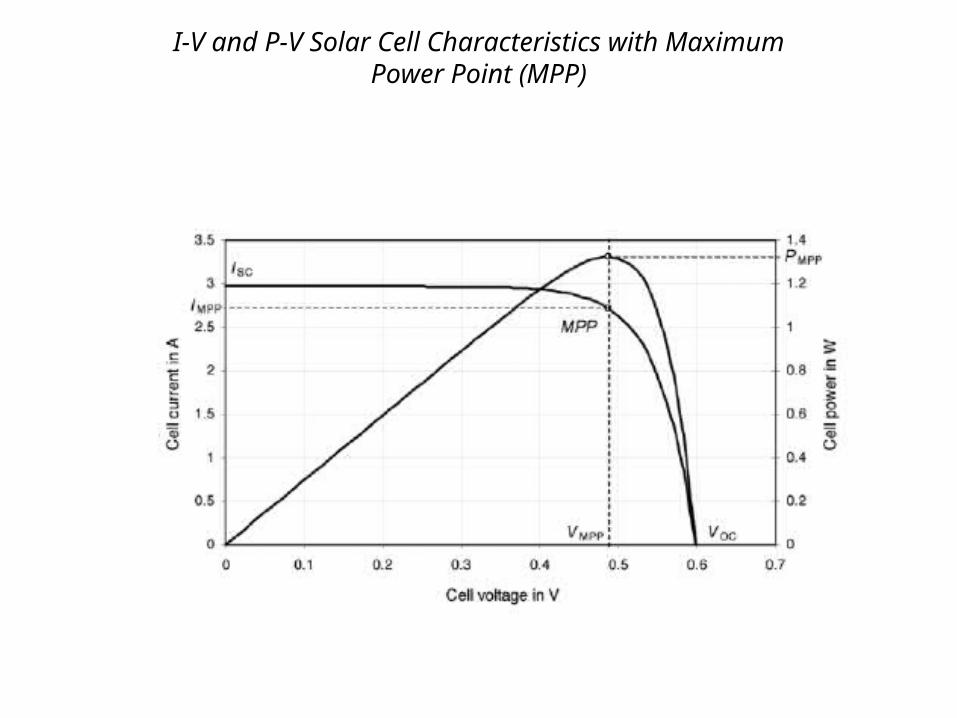
I-V and P-V Solar Cell Characteristics with MaximumPower Point (MPP)
Electrical solar cell parameters