solar energy materials & solar cells -...
TRANSCRIPT
Solar Energy Materials & Solar Cells 153 (2016) 18–24
Contents lists available at ScienceDirect
Solar Energy Materials & Solar Cells
http://d0927-02
n CorrE-m
journal homepage: www.elsevier.com/locate/solmat
Versatile strategies for improving the performance of diamond wiresawn mc-Si solar cells
Y.F. Zhuang a, S.H. Zhong a, Z.G. Huang a,b, W.Z. Shen a,c,n
a Institute of Solar Energy, and Key Laboratory of Artificial Structures and Quantum Control (Ministry of Education), Department of Physics and Astronomy,Shanghai Jiao Tong University, Shanghai 200240, People's Republic of Chinab School of Science, Huaihai Institute of Technology, Lianyungang 222005, Jiangsu Province, People's Republic of Chinac Collaborative Innovation Center of Advanced Microstructures, Nanjing 210093, People's Republic of China
a r t i c l e i n f o
Article history:Received 26 November 2015Received in revised form6 April 2016Accepted 7 April 2016
Keywords:Solar cellDiamond wire sawnMulticrystalline siliconMetal-catalyzed chemical etchingNano/micro-texture
x.doi.org/10.1016/j.solmat.2016.04.01448/& 2016 Published by Elsevier B.V.
esponding author.ail address: [email protected] (W.Z. Shen).
a b s t r a c t
Unlike conventional multi-wire sawn (CMWS) multi-crystalline silicon (mc-Si) wafers, diamond wiresawn (DWS) mc-Si wafers textured by conventional acidic solution of HF/HNO3 are not suitable for solarcells because visible saw marks set significant barriers in both cell performance and surface appearance.In this work, we have employed versatile strategies based on metal-assisted chemical etching (MACE)technique to eliminate the saw marks and realize effective surface textures on DWS mc-Si wafers,including nano-texture (N-T), micro-texture (M-T) and nano/micro-texture (N/M-T). Especially, benefit-ing from the tradeoff between optical gain and electrical loss, the efficiency of 18.45% for N/M-T basedDWS mc-Si solar cells with a standard wafer size of 156�156 mm2 is reported to be higher by anabsolute 0.57% compared with that of CMWS mc-Si solar cells (17.88%). Our work provides ways offabricating DWS mc-Si solar cells with high efficiencies and satisfactory visual appearance.
& 2016 Published by Elsevier B.V.
1. Introduction
Diamond wire sawing (DWS) technique is widely used in cut-ting hard and brittle non-metallic materials [1]. In the photovoltaic(PV) industry, DWS has been used in slicing single crystallinesilicon (sc-Si) and multi-crystalline silicon (mc-Si) in recent years.Compared with conventional multi-wire sawing (CMWS) withslurry of SiC abrasives, DWS has several advantages includinghigher productivity, lower material waste, higher precision incutting thin wafers and less surface mechanical damages [2–6].More importantly, the conversion efficiency (η) of DWS sc-Si solarcells is over 19% in a traditional industrial production line [7],which is comparable to the η of slurry sawn ones. Therefore, DWSis expected to become the mainstream technique for Si-basedsolar cells in the near future.
Unfortunately, the production of DWS mc-Si solar cells is not sosuccessful due to the ineffective surface texturization. In the PVindustry, acidic solution of HF/HNO3 is most commonly used infabricating CMWS mc-Si solar cells [8,9]. During the etching, thesurface defects are removed and micron-pits are formed randomly.Unlike CMWS wafers, which are characterized by a thickerdamaged layer with random distribution of broken crystals, a
lower rough surface with parallel deep saw marks is observed onDWS wafers [2,10]. Resulting from nonuniform etching of the sawmarks, DWS mc-Si wafers cannot form an effective texture by thismethod and the surface reflectance is still higher than 25% [8,11].Since 80% of mc-Si wafers will be sawn with diamond wires by2020 [12], it is an urgent affair to realize an effective texturemethod for DWS mc-Si wafers.
Although reactive ion etching is effective for texturization ofmc-Si wafers [13,14], it is not suitable for the PV industry due tothe high cost. On the other hand, recent researches shows thateffective surface textures with Si nanostructures can be easilyformed on silicon wafers by metal-assisted chemical etching(MACE) [15–18], which is simple, cost-effective and compatiblewith current production lines. In this study, we present versatilestrategies to realize effective surface textures on DWS mc-Siwafers based on the MACE technique, including nano-texture (N-T), micro-texture (M-T) and nano/micro-texture (N/M-T). We havedemonstrated that all the N-T, M-T and N/M-T based solar cellsexhibit higher η than the conventional micro-textured (CM-T)cells. Especially, for the N/M-T based cells, their average η isincreased by 0.57% absolutely, reaching 18.45% on a large wafersize of 156�156 mm2, which is attributed to its both better opticaland electrical properties. Furthermore, our results reveal that thesaw marks have negative influence on the electrical properties ofthe solar cells but fortunately can be resolved by our texturingmethods.
Y.F. Zhuang et al. / Solar Energy Materials & Solar Cells 153 (2016) 18–24 19
2. Experimental
2.1. Texturization of diamond wire sawn wafers
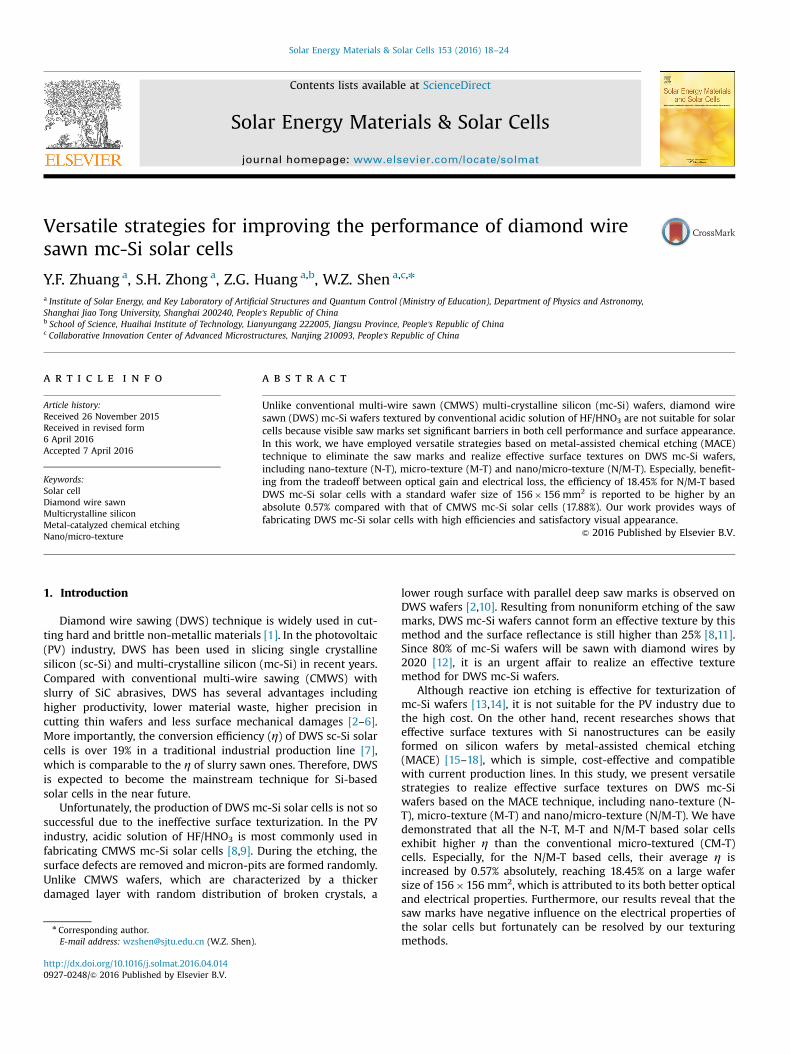
In this work, the used silicon wafers were p-type DWS mc-Siwith a size of 156�156 mm2, a thickness of 200720 μm andresistivity of 1–3Ω cm. The main steps for texturization of thewafers are shown in Fig. 1. Deionized water (DIW) cleaning wasperformed after every step. CM-T was prepared by immersing thewafers in the mixed acid solution of HF:HNO3:DIW¼1:5:4(volume ratio) for 3 min at 8 °C. N-T, M-T and N/M-T wereobtained by multiple-etching processes based on MACE technique.The wafers were firstly dipped into MACE solution (2.6 M HF/1.1 MH2O2/0.0002 M AgNO3) for 5 mins at 45 °C. In this process, Agnanoparticles were deposited onto the silicon and nano-holeswere obtained. After that, one group of the wafers were placedin the etching solution of NaOH (5 wt%) for 5 min to form the N-T.Another group of the wafers were immersed into the HF/HNO3
mixed solution for 3 min at 8 °C. As a result, nano-holes wereexpanded, and M-T was obtained. Then, a set of the M-T waferswere placed in MACE solution for 5 min again, followed by NaOHetching for 5 min to form the N/M-T. Finally, all the texturedwafers were immersed in the HNO3:DIW¼1:1 (volume ration) for10 min to remove the residual metal impurities, followed by rin-sing with DIW and spin-drying. Here, after all the processes, theremoving of the silicon wafers is about 3–4 μm on each side.
2.2. Fabrication of the DWS mc-Si solar cells
After the texturization, all the wafers underwent the samestandard industrial solar cell fabricating process, including diffu-sion, SiNx:H coating and screen printing. The wafers were firstlyplaced in a tube furnace for about 100 min at 800 °C by usingPOCl3 as doping source. Then, the phosphosilicate glass wasremoved by HF solution (9% by volume). After that, SiNx:H wasdeposited on the front surface as the antireflection and passivationlayer by plasma enhanced chemical vapor deposition for 40 min at400 °C. Finally, the fabrication of front and back electrodes wereperformed by the screen-printing, followed by a co-firing step at750 °C for 30 s.
Fig. 1. Schematic illustration of the main steps preparing
2.3. Characterization
The morphologies of the wafers were investigated by fieldemission scanning electron microscopy (FE-SEM) (Zeiss UltraPlus). The reflectance spectra together with the internal quantumefficiency (IQE) and external quantum efficiency (EQE) weremeasured by QEX10 (PV MEASUREMENTS). And the electricalparameters of the solar cells were measured under AM1.5 spec-trum at the temperature of 25 °C.
3. Result and discussion
3.1. The comparison of DWS and CMWS mc-Si wafers
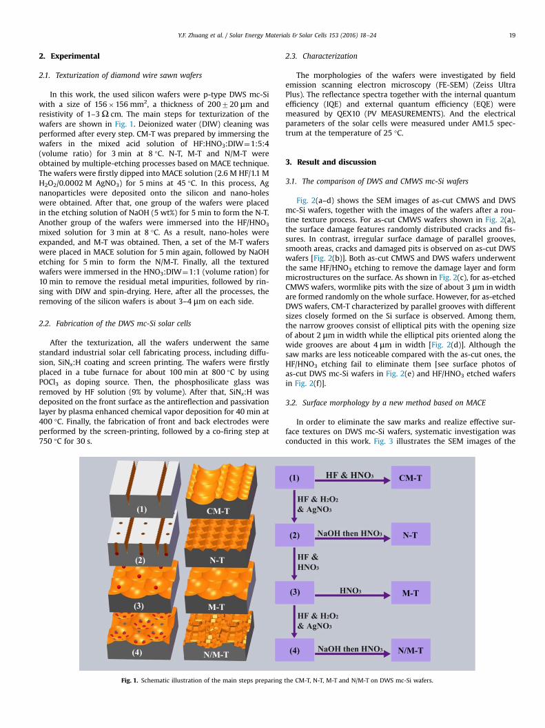
Fig. 2(a–d) shows the SEM images of as-cut CMWS and DWSmc-Si wafers, together with the images of the wafers after a rou-tine texture process. For as-cut CMWS wafers shown in Fig. 2(a),the surface damage features randomly distributed cracks and fis-sures. In contrast, irregular surface damage of parallel grooves,smooth areas, cracks and damaged pits is observed on as-cut DWSwafers [Fig. 2(b)]. Both as-cut CMWS and DWS wafers underwentthe same HF/HNO3 etching to remove the damage layer and formmicrostructures on the surface. As shown in Fig. 2(c), for as-etchedCMWS wafers, wormlike pits with the size of about 3 μm in widthare formed randomly on the whole surface. However, for as-etchedDWS wafers, CM-T characterized by parallel grooves with differentsizes closely formed on the Si surface is observed. Among them,the narrow grooves consist of elliptical pits with the opening sizeof about 2 μm in width while the elliptical pits oriented along thewide grooves are about 4 μm in width [Fig. 2(d)]. Although thesaw marks are less noticeable compared with the as-cut ones, theHF/HNO3 etching fail to eliminate them [see surface photos ofas-cut DWS mc-Si wafers in Fig. 2(e) and HF/HNO3 etched wafersin Fig. 2(f)].
3.2. Surface morphology by a new method based on MACE
In order to eliminate the saw marks and realize effective sur-face textures on DWS mc-Si wafers, systematic investigation wasconducted in this work. Fig. 3 illustrates the SEM images of the
the CM-T, N-T, M-T and N/M-T on DWS mc-Si wafers.
Fig. 2. SEM images of mc-Si wafers: (a) as-cut CMWS wafers (b) as-cut DWS wafers (c) routine textured CMWS wafers, and (d) routine textured DWS wafers. Surface photosof DWS mc-Si wafers: (e) as-cut wafers, and (f) HF/HNO3 etched wafers.
Y.F. Zhuang et al. / Solar Energy Materials & Solar Cells 153 (2016) 18–2420

Fig. 3. SEM images of the textured wafers: (a) N-T, (b) M-T, (c) N/M-T. (a0)–(c0) are the enlargements of (a)–(c), together with the SEM images of the cross-section of thewafers in the inset.
Y.F. Zhuang et al. / Solar Energy Materials & Solar Cells 153 (2016) 18–24 21
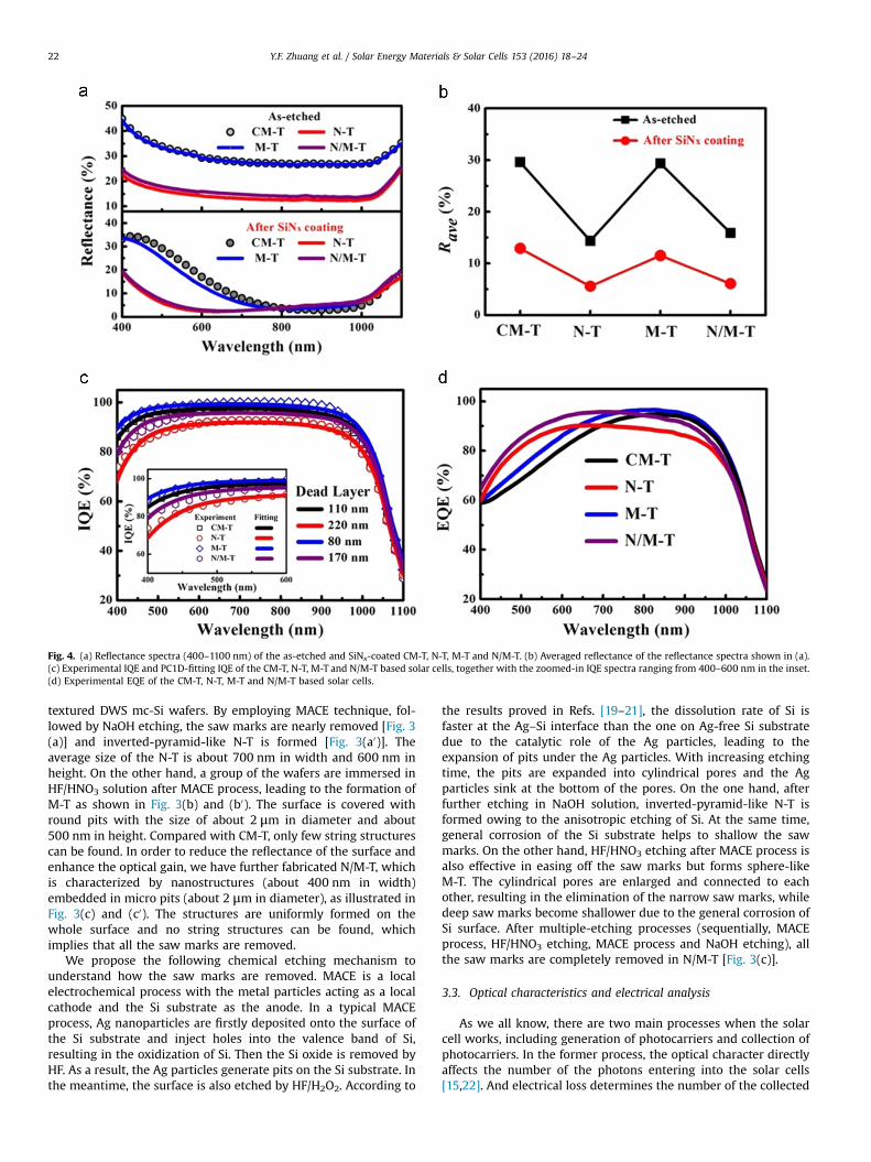
Fig. 4. (a) Reflectance spectra (400–1100 nm) of the as-etched and SiNx-coated CM-T, N-T, M-T and N/M-T. (b) Averaged reflectance of the reflectance spectra shown in (a).(c) Experimental IQE and PC1D-fitting IQE of the CM-T, N-T, M-T and N/M-T based solar cells, together with the zoomed-in IQE spectra ranging from 400–600 nm in the inset.(d) Experimental EQE of the CM-T, N-T, M-T and N/M-T based solar cells.
Y.F. Zhuang et al. / Solar Energy Materials & Solar Cells 153 (2016) 18–2422
textured DWS mc-Si wafers. By employing MACE technique, fol-lowed by NaOH etching, the saw marks are nearly removed [Fig. 3(a)] and inverted-pyramid-like N-T is formed [Fig. 3(a0)]. Theaverage size of the N-T is about 700 nm in width and 600 nm inheight. On the other hand, a group of the wafers are immersed inHF/HNO3 solution after MACE process, leading to the formation ofM-T as shown in Fig. 3(b) and (b0). The surface is covered withround pits with the size of about 2 μm in diameter and about500 nm in height. Compared with CM-T, only few string structurescan be found. In order to reduce the reflectance of the surface andenhance the optical gain, we have further fabricated N/M-T, whichis characterized by nanostructures (about 400 nm in width)embedded in micro pits (about 2 μm in diameter), as illustrated inFig. 3(c) and (c0). The structures are uniformly formed on thewhole surface and no string structures can be found, whichimplies that all the saw marks are removed.
We propose the following chemical etching mechanism tounderstand how the saw marks are removed. MACE is a localelectrochemical process with the metal particles acting as a localcathode and the Si substrate as the anode. In a typical MACEprocess, Ag nanoparticles are firstly deposited onto the surface ofthe Si substrate and inject holes into the valence band of Si,resulting in the oxidization of Si. Then the Si oxide is removed byHF. As a result, the Ag particles generate pits on the Si substrate. Inthe meantime, the surface is also etched by HF/H2O2. According to
the results proved in Refs. [19–21], the dissolution rate of Si isfaster at the Ag–Si interface than the one on Ag-free Si substratedue to the catalytic role of the Ag particles, leading to theexpansion of pits under the Ag particles. With increasing etchingtime, the pits are expanded into cylindrical pores and the Agparticles sink at the bottom of the pores. On the one hand, afterfurther etching in NaOH solution, inverted-pyramid-like N-T isformed owing to the anisotropic etching of Si. At the same time,general corrosion of the Si substrate helps to shallow the sawmarks. On the other hand, HF/HNO3 etching after MACE process isalso effective in easing off the saw marks but forms sphere-likeM-T. The cylindrical pores are enlarged and connected to eachother, resulting in the elimination of the narrow saw marks, whiledeep saw marks become shallower due to the general corrosion ofSi surface. After multiple-etching processes (sequentially, MACEprocess, HF/HNO3 etching, MACE process and NaOH etching), allthe saw marks are completely removed in N/M-T [Fig. 3(c)].
3.3. Optical characteristics and electrical analysis
As we all know, there are two main processes when the solarcell works, including generation of photocarriers and collection ofphotocarriers. In the former process, the optical character directlyaffects the number of the photons entering into the solar cells[15,22]. And electrical loss determines the number of the collected
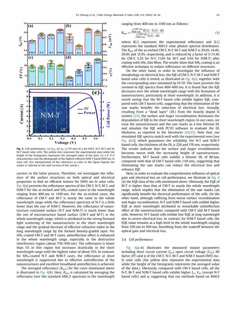
Fig. 5. Cell performance: (a) VOC, (b) ISC, (c) FF and (d) η for CM-T, N-T, M-T and N/M-T based solar cells. The yellow dots represent the experimental data while theheight of the histograms represents the averaged value of the data. (e) I–V, P–Vcharacteristics and the photograph of the highest-efficient N/M-T based DWS mc-Sisolar cell. (For interpretation of the references to color in this figure legend, thereader is referred to the web version of this article.)
Y.F. Zhuang et al. / Solar Energy Materials & Solar Cells 153 (2016) 18–24 23
carriers in the latter process. Therefore, we investigate the influ-ence of the surface structures on both optical and electricalproperties to find an efficient texture for DWS mc-Si solar cells.Fig. 4(a) presents the reflectance spectra of the CM-T, N-T, M-T, andN/M-T for the as-etched and SiNx-coated cases in the wavelengthranging from 400 nm to 1100 nm. For the as-etched cases, thereflectance of CM-T and M-T is nearly the same in the wholewavelength range while the reflectance spectrum of N-T is a littlelower than the one of N/M-T. However, the reflectance of nanos-tructure contained surface (N-T and N/M-T) is much lower thanthe one of microstructure based surface (CM-T and M-T) in thewhole wavelength range, which is attributed to the strong forwardlight scattering of the nanostructures in the short wavelengthrange and the gradual decrease of effective refractive index in thelong wavelength range by the formed density-graded layer. ForSiNx-coated CM-T and M-T cases, antireflection effect is enhancedin the whole wavelength range, especially in the destructiveinterference region (about 750–950 nm). The reflectance is lowerthan 5% in this region but increases drastically in the shortwavelength range with the highest value of about 35%. In contrast,for SiNx-coated N-T and N/M-T cases, the reflectance at shortwavelength is suppressed due to effective antireflection of thenanostructures and excellent broadband antireflection is achieved.
The averaged reflectance (Rave) for the cases mentioned aboveis illustrated in Fig. 4(b). Here, Rave is calculated by averaging thereflectance over the standard AM1.5 spectrum in the wavelength
ranging from 400 nm to 1100 nm as follows:
Rave ¼R 1100 nm400 nm R λ
� �US λ
� �Udλ
R 1100 nm400 nm S λ
� �Udλ
ð1Þ
where R(λ) represents the experimental reflectance and S(λ)represents the standard AM1.5 solar photon spectral distribution.The Rave of the as-etched CM-T, N-T, M-T and N/M-T is 29.6%, 14.4%,29.4% and 15.9%, respectively, and is reduced by a factor of 3 (11.4%for CM-T, 5.2% for N-T, 11.6% for M-T and 5.6% for N/M-T) aftercoating with SiNx thin films. The results show that SiNx coating is aneffective technique to reduce reflectance on different structures.
On the other hand, in order to investigate the influence ofmorphology on electrical loss, the IQE of CM-T, N-T, M-T and N/M-Tbased solar cells is tested, as illustrated in Fig. 4(c), together withthe corresponding ones simulated by PC1D. The inset presents thezoomed-in IQE spectra from 400–600 nm. It is found that the IQEdecreases over the whole wavelength range with the formation ofnanostructures, particularly at short wavelength. In addition, it isworth noting that the M-T based cells exhibit higher IQE, com-pared with CM-T based cells, suggesting that the elimination of thesaw marks benefits the reduction of electrical loss. Actually,resulting from a “dead layer” (DL) from the heavily doped Siemitter [23], the surface and Auger recombination dominates thedegradation of IQE in the short wavelength region. In our cases, wetreat the nanostructures and the saw marks as a low lifetime DLand simulate the IQE with PC1D software to evaluate the DLthickness, as reported in the literatures [24,25]. Note that, oursimulated IQE spectra match well with the experimental ones [seeFig. 4(c)], which guarantees the reliability. For N-T and N/M-Tbased cells, the thickness of the DL is 220 and 170 nm, respectively.The results indicate that the surface and Auger recombinationbecomes worse with the increasing height of nanostructures.Furthermore, M-T based cells exhibit a thinner DL of 80 nm,compared with that of CM-T based cells (110 nm), suggesting thateliminating the saw marks can reduce the electrical loss andenhance IQE.
Here, in order to evaluate the comprehensive influence of opticalgain and electrical loss on cell performance, we illustrate in Fig. 4(d) the EQE data of the cells mentioned above. Obviously, the EQE ofM-T is higher than that of CM-T in nearly the whole wavelengthrange, which implies that the elimination of the saw marks cansignificantly benefit the electrical performance of the cells. On theother hand, although suffering from worse surface recombinationand Auger recombination, N-T and N/M-T based cells exhibit higherEQE at short wavelength attributed to remarkable antireflectioneffect of the nanostructures, compared with CM-T and M-T basedcells. However, N-T based cells exhibit low EQE at long wavelengthdue to severe electrical loss. In contrast, for N/M-T based cells, theEQE value remains at a high level in the whole wavelength rangingfrom 550 nm to 950 nm, benefiting from the tradeoff between theoptical gain and electrical loss.
3.4. Cell performance
Fig. 5(a–d) illustrates the measured output parametersincluding short circuit current (Isc), open circuit voltage (Voc), fillfactor (FF) and η of the CM-T, N-T, M-T and N/M-T based DWS mc-Si solar cells (the yellow dots represent the experimental datawhile the height of the histograms represents the averaged valueof the data.). Obviously, compared with CM-T based cells, all theN-T, M-T and N/M-T based cells exhibit higher Isc, Voc (except N-Tbased cells) and η, suggesting that our methods based on MACE
Y.F. Zhuang et al. / Solar Energy Materials & Solar Cells 153 (2016) 18–2424
are effective for the texturization of DWS mc-Si solar cells. For N-Tbased cells, the Isc of 8.756 A is much higher than 8.617 A of CM-Tbased cells, which is attributed to the outstanding antireflectionperformance of the nanostructures, while the performancedegradation of VOC occurs due to the worse surface and Augerrecombination. On the other hand, resulting from less electricalloss by eliminating the saw marks, M-T based cells exhibit high VOC
of 634.3 mV, which is higher by 2.1 mV compared with 632.2 mVof the CM-T based cells, together with Isc of 8.743 A (higher thanthe one of CM-T based cells but a little lower than the one of N-Tbased cells). Moreover, benefiting from the tradeoff betweenoptical gain and electrical loss, N/M-T based cells exhibit goodperformance in both Isc and Voc and thus possess the highest η of18.45% among all the cells, which is higher by an absolute 0.57%compared with 17.88% of CM-T based cells. In addition, as shownin Fig. 5(c), the difference among the FF of the cells is not obvious,which implies that the surface morphology has nearly no influ-ence on FF. Fig. 5(e) presents the current–voltage (I–V) and power–voltage (P–V) characteristics of the N/M-T based solar cell, togetherwith the photograph of the cell. The maximum output powerreaches 4.49 W on the wafer size of 243.36 cm2, and the wholesurface of the cell exhibits the color of dark blue, which is asatisfying color in industry.
4. Conclusions
In summary, DWS mc-Si wafers cannot be effectively texturedby conventional methods due to the nonuniform etching of thesaw marks, exhibiting high reflectance (about 12% in average afterSiNx coating) and poor electrical properties. In this work, we havepresented effective texture methods for DWS mc-Si wafers basedon MACE technique. We have successfully fabricated high-efficiency N-T, M-T, N/M-T based DWS mc-Si solar cells on thestandard wafer size of 156�156 mm2. From the study of opticalcharacteristics, we find that the reflectance can be suppressed to alow level with the formation of nanostructures (about 5% inaverage after SiNx coating), especially at short wavelength. How-ever, at the same time, electrical loss from the surface recombi-nation and Auger recombination becomes severe owing to theheavily doped Si emitter. Benefiting from the tradeoff between theoptical gain and electrical loss, we have realized the N/M-T basedDWS mc-Si solar cells with a high η of 18.45%, which is higher byan absolute 0.57% compared with 17.88% of CM-T based cells. Notethat this technique also removes all the saw marks in DWS mc-Siwafers. Our work provides ways of fabricating DWS mc-Si solarcells with high efficiencies and satisfactory visual appearance.
Acknowledgments
This work was supported by the Natural Science Foundation ofChina (61234005, 11474201 and 11174202) and Natural ScienceFoundation of Jiangsu Province (BK20151284).
References
[1] W.H. Chen, X.M. Liu, M. Li, C.Q. Yin, L. Zhou, On the nature and removal of sawmarks on diamond wire sawn multicrystalline silicon wafers, Mater. Sci.Semicond. Process. 27 (2014) 220.
[2] N. Watanabe, Y. Kondo, D. Ide, T. Matsuki, H. Takato, I. Sakata, Characterizationof polycrystalline silicon wafers for solar cells sliced with novel fixed-abrasivewire, Prog. Photovolt. Res. Appl. 18 (2010) 485.
[3] B. Meinel, T. Koschwitz, J. Acker, Textural development of SiC and diamondwire sawed sc-silicon wafer, Energy Procedia 27 (2012) 330.
[4] W.I. Clark, A.J. Shih, C.W. Hardin, R.L. Lemaster, S.B. McSpadden, Fixed abrasivediamond wire machining—Part I: process monitoring and wire tension force,Int. J. Mach. Tools Manuf. 43 (2003) 523.
[5] A. Bidiville, K. Wasmer, R. Kraft, C. Ballif, Diamond wire-sawn silicon wafers-from the lab to the cell production, in: Proceedings of the 24th EU PV-SEC,2009.
[6] X.G. Yu, P. Wang, X.Q. Li, D.R. Yang, Thin Czochralski silicon solar cells based ondiamond wire sawing technology, Sol. Energy Mater. Sol. Cells 98 (2012) 337.
[7] K.X. Chen, Y.Y. Liu, X.S. Wang, L.J. Zhang, X.D. Su, Novel texturing process fordiamond-wire-sawn single-crystalline silicon solar cell, Sol. Energy Mater. Sol.Cells 133 (2015) 148.
[8] A. Kumagai, Texturization using metal catalyst wet chemical etching formulticrystalline diamond wire sawn wafer, Sol. Energy Mater. Sol. Cells 133(2015) 216.
[9] M. Lippold, F. Buchholz, C. Gondek, F. Honeit, E. Wefringhaus, E. Kroke, Tex-turing of SiC-slurry and diamond wire sawn silicon wafers by HF–HNO3–
H2SO4 mixtures, Sol. Energy Mater. Sol. Cells 127 (2014) 104.[10] A. Stapf, C. Gondek, M. Lippold, E. Kroke, HF–(NH4)2S2O8–HCl mixtures for
HNO3-and NOx‑free etching of diamond wire- and SiC-slurry-sawn siliconwafers: reactivity studies, surface chemistry, and unexpected pyramidal sur-face morphologies, ACS Appl. Mater. Interfaces 7 (2015) 16.
[11] F. Cao, K.X. Chen, J.J. Zhao, X.Y. Ye, J.J. Li, S. Zou, X.D. Su, Next-generation multi-crystalline silicon solar cells: diamond-wire sawing, nano-texture and highefficiency, Sol. Energy Mater. Sol. Cells 141 (2015) 132.
[12] S.A. Mann, M.J.D. Wild-Scholten, V.M. Fthenakis, The energy payback time ofadvanced crystalline silicon PV modules in 2020: a prospective study, Prog.Photovolt. Res. Appl. 22 (2014) 1180.
[13] K. Shirasawa, K. Fukui, K. Okada, Y. Inomata, H. Takahashi, Y. Fukawa, S. Fujii,Over 17% large area multicrystaline silicon solar cells, in: Proceedings of the14th EU PV-SEC, 1997.
[14] D.S. Rubya, S.H. Zaidi, S. Narayanan, B.M. Damianid, A. Rohatgi, Rie-texturing ofmulticrystalline silicon solar cells, Sol. Energy Mater. Sol. Cells 74 (2002) 133.
[15] F. Toor, H.M. Branz, M.R. Page, K.M. Jones, H.C. Yuan, Multi-scale surface tex-ture to improve blue response of nanoporous black silicon solar cells, Appl.Phys. Lett. 99 (2011) 103501.
[16] J.H. Oh, H.C. Yuan, H.M. Branz, An 18.2%-efficient black-silicon solar cellachieved through control of carrier recombination in nanostructures, Nat.Nanotechnol. 7 (2012) 743.
[17] Z.G. Huang, X.X. Lin, Y. Zeng, S.H. Zhong, X.M. Song, C. Liu, X. Yuan, W.Z. Shen,One-step-MACE nano/microstructures for high-efficient large-size multi-crystalline Si solar cells, Sol. Energy Mater. Sol. Cells 143 (2015) 302.
[18] S.H. Zhong, Z.G. Huang, X.X. Lin, Y. Zeng, Y.C. Ma, W.Z. Shen, High-efficiencynanostructured silicon solar cells on a large scale realized through the sup-pression of recombination channels, Adv. Mater. 27 (2015) 555.
[19] S.Y. Li, W.H. Ma, Y. Zhou, X.H. Chen, Y.Y. Xiao, M.Y. Ma, F. Wei, X. Yang, Fab-rication of p-type porous silicon nanowire with oxidized silicon substratethrough one-step MACE, J. Solid State Chem. 213 (2014) 242.
[20] Z.P. Huang, N. Geyer, P. Werner, J.D. Boor, U. Gösele, Metal-assisted chemicaletching of silicon: a review, Adv. Mater. 23 (2011) 285.
[21] C. Chartier, S. Bastide, C. Le´vy-Cle´ment, Metal-assisted chemical etching ofsilicon in HF–H2O2, Electrochim. Acta 53 (2008) 5509.
[22] Z.G. Huang, S.H. Zhong, X. Hua, X.Y. Kong, N. Dai, W.Z. Shen, An effective wayto simultaneous realization of excellent optical and electrical performance inlarge-scale Si nano/microstructures, Prog. Photovolt. Res. Appl. 23 (2015) 964.
[23] J.Y. Kim, M.K. Kwon, V.J. Logeeswaran, S. Grego, M.S. Islam, Post-growth in situchlorine passivation for suppressing surface-dominant transport in siliconnanowire devices, IEEE Trans. Nanotechnol. 11 (2012) 782.
[24] X.X. Lin, X. Hua, Z.H. Huang, W.Z. Shen, Realization of high performance siliconnanowire based solar cells with large size, Nanotechnology 24 (2013) 235402.
[25] H.C. Yuan, V.E. Yost, M.R. Page, P. Stradins., D.L. Meier, H.M. Branz, Efficientblack silicon solar cell with a density-graded nanoporous surface: opticalproperties, performance limitations, and design rules, Appl. Phys. Lett. 95(2009) 123501.