solar home systems - documents & reports - all...
TRANSCRIPT

Solar Home SystemsManual for the Design and Modification of Solar Home System Components
M. R.VervaartF. D. J. Nieuwenhout
ECN—Netherlands Energy Research FoundationPetten,The Netherlands
34072
Pub
lic D
iscl
osur
e A
utho
rized
Pub
lic D
iscl
osur
e A
utho
rized
Pub
lic D
iscl
osur
e A
utho
rized
Pub
lic D
iscl
osur
e A
utho
rized
Pub
lic D
iscl
osur
e A
utho
rized
Pub
lic D
iscl
osur
e A
utho
rized
Pub
lic D
iscl
osur
e A
utho
rized
Pub
lic D
iscl
osur
e A
utho
rized

Copyright © 2001 The International Bank for Reconstruction and Development / THE WORLD BANK1818 H Street, N.W.Washington, D.C. 20433, USA
All rights reservedManufactured in the United States of AmericaFirst printing January 2001
The findings, interpretations, and conclusions expressed in this book areentirely those of the authors and should not be attributed in any mannerto the World Bank, to its affiliated organizations, or to members of itsBoard of Executive Directors or the countries they represent. The WorldBank does not guarantee the accuracy of the data included in this publi-cation and accepts no responsibility for any consequence of their use.The boundaries, colors, denominations, and other information shown onany map in this volume do not imply on the part of the World BankGroup any judgment on the legal status of any territory or the endorse-ment or acceptance of such boundaries.
The material in this publication is copyrighted. The World Bank encour-ages dissemination of its work and grants permission to reproduce thiswork.

Table of ContentsPreface............................................................................................................................................................................................................viii
Acknowledgments..................................................................................................................................................................................ix
Chapter 1:Experience with Solar Home Systems ............................................................................................................................ 1
1.1 Introduction ........................................................................................................................................................................................ 11.2 Nontechnical Aspects Relevant for System Sizing and Design................................................................................................ 2
1.2.1 Costs ...................................................................................................................................................................................... 21.2.2 Ownership ............................................................................................................................................................................ 21.2.3 After-Sale Services .............................................................................................................................................................. 31.2.4 Feedback from Field Experience ...................................................................................................................................... 31.2.5 Environmental Issues .......................................................................................................................................................... 4
1.3 Technical Aspects ................................................................................................................................................................................ 41.3.1 System Losses ...................................................................................................................................................................... 41.3.2 Sizing of the PV Module .................................................................................................................................................... 61.3.3 Sizing of Components ........................................................................................................................................................ 71.3.4 Modularity.............................................................................................................................................................................. 8
1.4 Solar Home System Components ................................................................................................................................................ 81.4.1 Modules .................................................................................................................................................................................. 81.4.2 Module Support Structure ................................................................................................................................................ 91.4.3 Battery Charge Regulator................................................................................................................................................ 101.4.4 Battery.................................................................................................................................................................................. 111.4.5 Battery Mounting .............................................................................................................................................................. 141.4.6 Lamps, Ballasts, and Fixtures .......................................................................................................................................... 141.4.7 Wiring, Switches, and Outlets ........................................................................................................................................ 151.4.8 Inverters .............................................................................................................................................................................. 16
Chapter 2:Lighting in Solar Home Systems........................................................................................................................................ 17
2.1 Design Considerations for Lights..................................................................................................................................................172.1.1 Types of Lighting ................................................................................................................................................................ 172.1.2 Luminous Flux .................................................................................................................................................................... 182.1.3 Luminous Efficacy .............................................................................................................................................................. 192.1.4 Illuminance .......................................................................................................................................................................... 192.1.5 Measurements of Luminous Flux .................................................................................................................................. 20
2.2 Fluorescent Lamp Inverters (FLIs) ................................................................................................................................................212.2.1 Introduction ........................................................................................................................................................................ 212.2.2 Working Principle of a Fluorescent Light .................................................................................................................... 222.2.3 Blackening of the Fluorescent Lamp ............................................................................................................................ 232.2.4 Lamp Inverters with One or Two Transistors ............................................................................................................ 262.2.5 Different Transistor Set-Ups............................................................................................................................................ 272.2.6 Polarity Protection ............................................................................................................................................................ 332.2.7 Field-Effect Transistor (FET) versus Transistor ............................................................................................................ 332.2.8 Effect of Filament Preheating .......................................................................................................................................... 342.2.9 Critical Components and Component Quality.......................................................................................................... 362.2.10 Inductance Calculation of the Transformer Coil ........................................................................................................ 412.2.11 EMC and PCB Design ...................................................................................................................................................... 43
iiiSolar Home Systems

Chapter 3:Charge Regulators ........................................................................................................................................................................ 45
3.1 Introduction ...................................................................................................................................................................................... 453.2 Objectives and Scope of Work .................................................................................................................................................... 453.3 Design Ideas ...................................................................................................................................................................................... 46
3.3.1 Series and Shunt-Type Regulator: Pros and Cons...................................................................................................... 463.3.2 Positive Switching and Negative Switching .................................................................................................................. 483.3.3 HVD Switching in the Battery Line: Pros and Cons ................................................................................................ 493.3.4 ON-OFF Charging and PWM Charging ...................................................................................................................... 513.3.5 Boost Charging .................................................................................................................................................................. 543.3.6 Special Function ICs.......................................................................................................................................................... 553.3.7 Digital or Analog Set-Up.................................................................................................................................................. 56
3.4 Modification Points.......................................................................................................................................................................... 573.4.1 Quiescent Current Reduction........................................................................................................................................ 573.4.2 Safety Precautions: Reverse Polarity Protection ........................................................................................................ 603.4.3 Reduction of the Number of Components ................................................................................................................ 603.4.4 Safety Precautions: Overload Protection and Short Circuit Protection .............................................................. 613.4.5 Lightning Surge Induction ................................................................................................................................................ 623.4.6 Oscillation Problems without Battery .......................................................................................................................... 64
Chapter 4:DC–AC Conversion.................................................................................................................................................................... 67
4.1 Scope of Work.................................................................................................................................................................................. 674.2 Types of Inverter: Principles .......................................................................................................................................................... 684.3 DC Voltage Supply Imperfection Input Filter ............................................................................................................................ 714.4 Single-Phase Inverters Topologies ................................................................................................................................................ 73
4.4.1 Single-Phase Inverter with Center-Tapped Transformer .......................................................................................... 734.4.2 Single-Phase Half-Bridge Inverter .................................................................................................................................. 744.4.3 Single-Phase Full-Bridge Inverter.................................................................................................................................... 75
4.5 Galvanic Isolation ............................................................................................................................................................................ 764.6 Comparison of the Required Components and Characteristics ........................................................................................ 794.7 Square-Wave versus PWM Switching ........................................................................................................................................ 80
4.7.1 Square-Wave Switching Principle .................................................................................................................................. 804.7.2 PWM Switching Scheme .................................................................................................................................................. 80
4.8 Semiconductor Switches and Driver Circuits .......................................................................................................................... 824.8.1 Semiconductor Switches.................................................................................................................................................. 824.8.2 Gate and Base Drive Circuits ........................................................................................................................................ 84
4.9 Component Temperature Control and Heat Sinks ................................................................................................................ 934.9.1 Control of Semiconductor Device Temperatures...................................................................................................... 934.9.2 Heat Transfer by Conduction.......................................................................................................................................... 94
4.10 Examples.......................................................................................................................................................................................... 954.10.1 150VA High-Frequency Inverter .................................................................................................................................... 954.10.2 DC-AC Isolated Battery Inverter Using the Integrated Circuit HIP4082 .......................................................... 97
Chapter 5:Advisory Services Body for Improving BOS Components ...................................................................... 101
5.1 Establishing an Advisory Services Body .................................................................................................................................. 1015.2 Procedures of an Advisory Services Body .............................................................................................................................. 102
ivSolar Home Systems

Chapter 6:Practical Part of the Training Course.......................................................................................................................... 103
6.1 Fluorescent Lamp Inverters ........................................................................................................................................................ 1036.1.1 Measuring Fluorescent Lamp Inverters ...................................................................................................................... 1036.1.2 Modifications .................................................................................................................................................................... 104
6.2 Charge Regulators ........................................................................................................................................................................ 1046.2.1 General .............................................................................................................................................................................. 1046.2.2 Measurements .................................................................................................................................................................. 1056.2.3 Modifications .................................................................................................................................................................... 105
6.3 DC-AC Converters...................................................................................................................................................................... 1066.3.1 General................................................................................................................................................................................1066.3.2 Measurements at DC-AC Converters ...................................................................................................................... 1066.3.3 Modifications .................................................................................................................................................................... 106
Appendix 1: Positive Switching Charge Regulator ................................................................................................ 107
Appendix 2: Block Diagram of a Modified Charge Regulator .................................................................... 108
Appendix 3: Data Sheet IRFZ40 .......................................................................................................................................... 109
Appendix 4: Negative Switching Shunt Regulator ................................................................................................ 110
Appendix 5: Negative Switching Shunt Regulator with E-Fuse .................................................................. 111
Appendix 6: Positive Switching Charge Regulator with E-Fuse.................................................................. 112
Appendix 7: 200VA HF Full-Bridge Inverter .............................................................................................................. 113
Appendix 8: HF Full-Bridge Inverter Using Integrated Circuit HIP4082 ............................................ 114
Appendix 9: Introduction to Light and Lighting ...................................................................................................... 117
Appendix 10: Equipment Needed for Practical Part of the Training Course.................................. 119
Appendix 11: Training Program Evaluation .................................................................................................................. 120
Appendix 12: Sample Checklist ............................................................................................................................................ 123
Abbreviations and Special Terms .......................................................................................................................................... 125
References ............................................................................................................................................................................................127
Viewgraphs
List of FiguresFigure 1.1. Basic Set-Up of a Solar Home System ...................................................................................................................... 1Figure 1.2. Breakdown of the Investment Cost of Solar Home System Components ...................................................... 3Figure 1.3. The Effect of Temperature on a Solar Cell .............................................................................................................. 9Figure 1.4. Temperature Coefficients of a Multicrystalline PV Module, Measured at ECN in 1999 ............................ 10Figure 1.5. Different States While Charging a Battery ............................................................................................................ 13Figure 1.6. Assembly of a Compact Fluorescent Lamp in Botswana .................................................................................... 14
Figure 2.1. A DC Light from Goldstar that Can be Used for General or Localized Lighting ........................................ 18Figure 2.2. Cluster LED Lamp from Steca .................................................................................................................................. 18Figure 2.3. Luminous Flux (lumen) and Energy Consumption (watt) for 35 Lights Measured by ECN ...................... 19Figure 2.4. Luminous Efficacy (lumen/watt) of All Lights Included in the Test Sample.................................................... 19Figure 2.5. Illuminance (lux) and Illuminous Efficacy (lux/watt) in a Horizontal Plane
1 Meter Below the Light Source .............................................................................................................................. 20
vSolar Home Systems

Figure 2.6. Ulbright Sphere for the Measurement of Luminous Flux .................................................................................. 20Figure 2.7. Schematic Diagram of a Fluorescent Tube Light .................................................................................................. 22Figure 2.8. Two Examples of a Waveform of a One-Transistor DC-FLI ............................................................................ 26Figure 2.9. Waveform of a Two-Transistor DC-FLI ................................................................................................................ 27Figure 2.10. Well-Trimmed Transistor Takeover ........................................................................................................................ 27Figure 2.11. The Chopper Design .................................................................................................................................................. 28Figure 2.12. The Push-Pull Configuration ...................................................................................................................................... 28Figure 2.13. Diagram of the Ballast Circuit: Example Set-Up 1 ................................................................................................ 29Figure 2.14. Diagram of the Ballast Circuit: Example Set-Up 2 ................................................................................................ 30Figure 2.15. Diagram of the Ballast Circuit: Example Set-Up 3 ................................................................................................ 31Figure 2.16. Diagram of the Ballast Circuit: Example Set-Up 4 ................................................................................................ 32Figure 2.17. Polyswitch Characteristics .......................................................................................................................................... 33Figure 2.18. The Use of a MOSFET for Polarity Protection .................................................................................................... 33Figure 2.19. Example of MOSFET Use in FLI................................................................................................................................ 34Figure 2.20. Configuration for Filament Preheating .................................................................................................................... 35Figure 2.21. Filament Preheating with Parallel Capacitor .......................................................................................................... 35Figure 2.22. Starting Sequence of an FLI........................................................................................................................................ 36Figure 2.23. Power Loss during Transistor Switching ................................................................................................................ 36Figure 2.24. Capacitor across Primary Winding of Transformer ............................................................................................ 38Figure 2.25. Inductor in Series with Primary Side of the Transformer.................................................................................. 39Figure 2.26. Capacitor and Inductor in Series with Tube Lamp .............................................................................................. 40Figure 2.27. Emitter Inverter with Tapped Feedback Winding .................................................................................................. 42Figure 2.28. FLI Set-up for Demonstrating Flux Saturation ...................................................................................................... 42Figure 2.29. Core Saturation Area .................................................................................................................................................. 43Figure 2.30. Skin Effect in a Lead-Acid Battery ............................................................................................................................ 44Figure 2.31. Decrease in Efficiency Caused by PCB Design...................................................................................................... 44
Figure 3.1. System Set-up in a Shunt-Type Controller ............................................................................................................ 46Figure 3.2. Basic Diagram of a Serial, Negative-Switching SHS Controller ........................................................................ 47Figure 3.3. Basic Diagram of a Positive-Switching SHS Controller ...................................................................................... 49Figure 3.4. Basic System for HVD-Switching in the Battery Line .......................................................................................... 50Figure 3.5. Low-Cost ON-OFF Charge Regulator .................................................................................................................... 51Figure 3.6. Charging Current Acceptance from a Lead Acid Battery .................................................................................. 52Figure 3.7. Block Diagram for Constant Voltage PWM Algorithm ...................................................................................... 53Figure 3.8. Morningstar’s SunSaver Charge Regulator.............................................................................................................. 53Figure 3.9. SunSaver-6 PWM Results: Voltage against Time for Three Different Duty Cycles ...................................... 54Figure 3.10. ON-OFF Charge Regulator Based on Integrated Circuit .................................................................................. 56Figure 3.11. PWM Charge Regulator Based on Integrated Circuit ........................................................................................ 56Figure 3.12. Example of a Microprocessor-Based Charge Regulator...................................................................................... 58Figure 3.13. Reference Voltage with Zener Diode ...................................................................................................................... 59Figure 3.14. IC Replaces Zener Diode .......................................................................................................................................... 59Figure 3.15. The IEC Standard Test Pulse for Testing the Transient Overvoltage Protection ........................................ 63Figure 3.16. Transient Voltage Drops in Solar Home Systems.................................................................................................. 64
Figure 4.1. 250–500 Watt DC-AC Inverter from LUE ............................................................................................................ 68Figure 4.2. Basic Diagram of a Full Bridge .................................................................................................................................. 69Figure 4.3. Basic Diagram of an Autonomous Voltage Inverter ............................................................................................ 69Figure 4.4. Inductive Load Waveforms ........................................................................................................................................ 70Figure 4.5. Capacitative Load Waveforms .................................................................................................................................. 70Figure 4.6. Waveforms...................................................................................................................................................................... 71
viSolar Home Systems

Figure 4.7. Correcting the DC Voltage Supply .......................................................................................................................... 72Figure 4.8. Notations for a Single-Phase Voltage-Source Inverter with Two Switches and a
Center-Tapped Primary Transformer...................................................................................................................... 73Figure 4.9. Single-Phase Half-Bridge Configuration .................................................................................................................. 74Figure 4.10. Full-Bridge Structure .................................................................................................................................................... 75Figure 4.11. Transformer Representations: (a) Typical B-H Loop Transformer Core,
(b) Two-Winding Transformer, (c) Equivalent Circuit ........................................................................................ 77Figure 4.12. 3C8 Ferrite Characteristics Curve: (a) B-H Loop, (b) Core Losses Curves.................................................. 77Figure 4.13. High-Frequency Transformer with Bidirectional Core Excitation (Using Full-Bridge Topology) ............ 78Figure 4.14. Square-Wave Switching .............................................................................................................................................. 80Figure 4.15. Pulse-Width Modulation ............................................................................................................................................ 81Figure 4.16. MOSFET Characteristics ............................................................................................................................................ 83Figure 4.17. IGBT Characteristics.................................................................................................................................................... 84Figure 4.18. MOSFET Gate Drive Circuit Suitable for Low-Speed and Low-Switching
Frequency Applications .............................................................................................................................................. 85Figure 4.19. A MOSFET Gate-Drive Circuit with a Totem-Pole Configuration for Faster Turn-Off Times................ 86Figure 4.20. Various Gate-Drive Circuits ...................................................................................................................................... 87Figure 4.21. Optocoupler Isolation of Base-Drive Circuits ...................................................................................................... 88Figure 4.22. Transformer-Isolated MOSFET Gate-Drive Circuit Using High-Frequency Carriers .................................. 89Figure 4.23. Overcurrent Protection .............................................................................................................................................. 90Figure 4.24. Circuit for Providing Blanking Time ........................................................................................................................ 91Figure 4.25. Circuit Layout and the Interconnection Considerations in Connecting Base-Drive
Circuits to Power BJTs................................................................................................................................................ 92Figure 4.26. An Isolated Rectangular Rod that Conducts P Watts of Heat Energy per Unit Time .............................. 94Figure 4.27. Steady-State Heat Flow and Thermal Resistance in a Multiple-Layer Structure Including a
(a) Heat Sink and (b) Equivalent Circuit Based on Thermal Resistors............................................................ 95Figure 4.28. 150-Watt DC-AC Converter from ELV GmbH.................................................................................................... 96Figure 4.29. Block Diagram of a High-Frequency DC-AC Converter.................................................................................... 96
Figure 6.1. Wrong Output-Power Measurement .................................................................................................................... 104
List of TablesTable 1.1. Typical Costs and Expected Lifetime Figures for a 40 Wp SHS .......................................................................... 2Table 1.2. Energy Losses .................................................................................................................................................................. 6Table 1.3. Cable Gauge in 12 Vdc Systems ................................................................................................................................ 15
Table 2.1. Some Types of Capacitors ........................................................................................................................................ 41
Table 3.1. Special Function ICs for Charge Regulators .......................................................................................................... 57
viiSolar Home Systems

Preface
Solar photovoltaics is one of the most cost-effective ways of providingsmall amounts of electricity to areas without a power grid. Especiallyin places where people live in scattered houses, the cost of alternatives
for providing electricity usually is prohibitively high. Solar home systems(SHSs) are small systems designed to meet the electricity demand of a singlehousehold. A solar home system always consists of one or more photovolta-ic (PV) modules and a battery, and a load consistingof lights and sockets for radio, television, or appli-ances. A battery charge regulator is usually addedto control charging and discharging of the battery.
This manual has two major objectives: To provide necessary background material for the
modification of existing designs of solar homesystem components, especially the battery chargeregulator, inverters for fluorescent lamps, andDC–AC inverters.
To provide background material for completelynew designs of solar home system components.The target audience for this manual is primarily
engineers in companies producing solar home sys-tem components. Engineers in solar energy research institutes also wouldbenefit from the information provided.
The solar PV module is by far the most reliable component of a solarhome system. Relatively few problems are associated with the PV module.Therefore, we limit ourselves to the designs of the rest of the components,the so-called balance of system (BOS) components. PV systems will be dis-cussed, but only for systems with a power level appropriate tohousehold demands. Aspects of batteries important for BOS com-ponents also will be discussed.
Because building practices depend very much on local customsand sometimes on regulations, this manual does not discuss to anygreat extent the support structure for the modules, but focuses onthe electrical and electronic components. The emphasis is on thebattery charge regulator because it is the single most critical com-ponent in a solar home system. Lights are the only appliances dis-cussed in this manual. Lighting is included in most solar home sys-tems, and the lights usually are provided with the system. Some ofthe larger solar home systems also can be equipped with a DC–ACinverter to allow the use of larger AC appliances.
In this manual we have limited ourselves to user experiences rel-evant for design of technical and nontechnical aspects of solarhome systems. Financial aspects will be mentioned in relation todesign and system sizing. Institutional settings, ownership issues,financing schemes and after sales arrangements will not be dis-cussed, although these aspects are also critical to the success of solar homesystem dissemination.
viiiSolar Home Systems
Above: A solar home system inSukatani, IndonesiaBelow: Two residents promotethe use of solar home systemsin Botswana

Acknowledgments We would like to thank Mr. Gulsham Kapur, and Professor H. Saha, the
two peer reviewers present during the training in India, for their valuableand detailed comments. Furthermore, we are grateful for the comments onthe draft text provided by Messrs. Bengt Perers of Vattenfall, Sweden; KeithPresnell of the Northern Territory University of Darwin, Australia; MichelVilloz of Dynatex SA, Switzerland; and Jeroen van Twisk, Jan Pierik, andJaap Eikelboom of ECN.
ixSolar Home Systems

xSolar Home Systems

Chapter 1Experience with Solar Home Systems
1.1 Introduction
Early in 1999, about 1 million solar home systems were in use in theworld, and this number is growing rapidly. This is a strong indica-tion that this technology provides desired services to rural house-
holds in areas without an electrical power grid. Technical and nontechnicalproblems often arise, however, which canhamper the further wide-scale application ofsolar home systems in rural electrification.From time to time in this report, experiencesin different countries are documented or sum-marized. Engineers who are involved in thedesign of solar home systems and their com-ponents can learn from these experiences.Those system designs that take into accountthe demands of the users will be the mostsuccessful in the marketplace.
This chapter describes some of the findingsthat are most relevant for design engineers ofsolar home systems. A number of nontechni-cal aspects are included because these areimportant to guide design activities.
A solar home system, as shown in figure1.1, can be defined as a small, autonomousphotovoltaic (PV) system that consists of oneor more solar modules, a battery and several12Vdc appliances.
During daylight the battery is charged. Thestored energy can be used for generating lightand running a television set or radio duringthe evening. When the battery is fullycharged, the regulator disconnects the mod-ule in order to prevent the battery frombecoming damaged. This moment is calledHigh Voltage Disconnect (HVD). Below a cer-tain level of discharge the battery can also bedamaged. Therefore the regulator disconnectsthe load before the battery is completelydrained. This moment is called Low VoltageDisconnect (LVD).
1Solar Home Systems
Lectures, Day 1
Photovoltaicelectricitygenerator
Figure 1.1Basic Set-up of a Solar Home System
Solar modules
Regulator
Battery Intercom
20 watt TV
8 watt FLs
8 watt FLs
8 watt FLs
12 voltappliances
8 wattradio/tape

1.2 Nontechnical Aspects Relevant for System Sizing and Design
1.2.1 CostsIn the investment cost of a solar home system, the PV module takes the
major share of about 65 percent of the initial cost. Batteries take about 13percent and the battery charge controller about 5 percent. Reducing thecost of the modules clearly is very important to making solar home systemsmore affordable to the rural poor.
Different components in a solar home system have different lifetimes.Modules can last for 20 years or more. Batteries, however, last for about threeyears, or as little as two years in some countries. The total costs of the differ-ent components, over a life cycle of 20 years, present a different picture thanfor the initial costs. The PV module, which contributes 65 percent of the ini-tial investment cost, accounts for only 33 percent of the life cycle cost, whilethe cost of batteries increases from 13 percent to 46 percent, substantiallygreater than the life-cycle cost of the modules.1 Over a 20-year period, thecost of the battery charge controller remains unchanged at 5 percent (see figure 1.2). To reduce the 20-year cost of solar home systems, it is thereforeof utmost importance to increase the lifetime of the batteries used. Higherquality battery charge regulators are thus an essential requirement. Table 1.1shows some typical figures for costs and lifetime of the different componentsof a solar home system. These figures have been used to calculate the valuespresented in figure 1.2.
1.2.2 OwnershipThere is a wide range of institu-
tional and financial arrangementsin solar home system projects.Ownership varies from completeownership of the users in com-mercial distribution systems tostate ownership of some govern-ment projects. In between arecredit schemes, in which the usereventually will own the systemafter the loan has been complete-ly repaid.
Ownership transpires to be animportant factor in the attitude of people toward their PV systems. A senseof ownership is a strong incentive for maintaining the system. For this rea-son, projects where the government provides the systems at no charge usu-ally show much higher failure rates than commercial schemes.
If known in advance, design engineers can take into account ownershipof solar home systems. Especially in the case of publicly owned systems(owned by either governments or utilities), it is necessary to ensure that
2Solar Home Systems
1 Calculated as the undiscounted life-cycle cost over a period of 20 years.
Table 1.1.Typical Costs and Expected Lifetime Figures for a 40 Wp SHS
Component Cost (U.S. dollars) Lifetime (years)
Module (40 Wp) 240 20Battery 50 3Controller 20 10Light fixtures (2 pieces) 20 10Fluorescent tubes (2 pieces) 2 1Mounting materials, cables 40 20
Total 372

only a minimum amount of maintenance is necessary, and to expect thatsometimes there will be no maintenance at all.
Often, aspects of ownership, quality of the products, and service provid-ed after the sale are related to the financial success of the disseminationactivity. Lower quality products and the absence of after-sales services gen-erally lead to high default rates in financing schemes.
1.2.3 After-Sale ServicesUsers of solar home systems must be able to get their equipment re-
paired in local workshops. The costs of replacement parts and labor can becovered by a guarantee arrangement, or by a fee-for-service arrangement. Ifnot, the user has to bear all the costs. In all cases, cost savings can beachieved when products of high quality are used. Maintenance and repaircosts are substantially higher when products are of poor quality. An analy-sis of the lifetime of a solar home system shows that it is usually worthinvesting in improved quality. This is especially the case for the batterycharge regulator.
1.2.4 Feedback from Field ExperienceIn most countries, distribution of solar home systems starts with PV
modules in the range of 35 to 50 watt-peak. After some time, growth stag-nates because the majority of people in rural areas cannot afford the fullcost. But more people appear to be able to afford the cost of smaller sys-tems of 10 to 20 watts. This illustrates the need to listen carefully to therequirements of the users.
3Solar Home Systems
Controller5%
Rest17%
Initial cost
Figure 1.2Breakdown of the Investment Cost of Solar Home System Components
Batteries13%
Modules65%
Note: The initial investments are shown on the left, and the shares in the life-cycle are shown on the right.
Controller5%
Rest16%
Life-cycle cost
Batteries46%
Modules33%

There are two main channels of information. Through after-sale serviceworkshops, it is possible to learn how often certain components fail.Ideally, all problems and complaints should be registered. Another channelis the distribution network, which provides information regarding thedemand for certain (sizes) of systems. The larger the range of products, themore market information can be obtained in this way.
Very little information is available about the actual use of solar home sys-tems in practice. There are some scattered monitoring activities. Whereavailable, they provide very useful data about the sizing of the systems andrelative sizing of the components, for example.
1.2.5 Environmental IssuesBatteries constitute a major concern in the environmental effects of large-
scale implementation of solar home systems. Batteries can be recycled, butthe recycling process can be harmful to the environment. Designers ofcharge regulators can contribute to the extension of the lifetime of a battery.
1.3 Technical Aspects
1.3.1 System LossesBefore the system sizing can begin, system losses must be estimated.
When the amount of energy that the user needs is known, the size of themodule can be calculated. Then the battery size can be chosen, taking intoaccount all the other factors.
The first step is to define the different factors that contribute to the sys-tems’ energy loss. All the available energy starts at the module, so we beginwith loss factors there.
PV module output losses: Orientation. Mostly the module is mounted in a fixed position. For every
location on earth there is one direction and tilt angle that results in thegreatest amount of annual electricity generation, or for the highestamount generated during the darkest month, whichever of the two is required. However, this is not critical. When the direction is withinabout 20 degrees of the optimum direction and the tilt angle within 10 degrees of the optimum angle, the electricity generated is within 5 percent of the optimum.
Shading of the module. During part of the day, the module may be shadedby a tree or building. Compared to a module in an open site, this meansenergy loss. Furthermore, it is important to note that trees grow. After acouple of years a tree could start shading a part of the module.
Dust on the module. Modules need to be as clean as possible. Dustbuilds up on the surface of the module, especially in the dry season.Therefore, never install a module with an inclination angle of less thanabout 15 degrees, to allow the rain to clean the panel. This dust causesenergy losses that can be as high as 5-10 percent even in areas with fre-quent rain.
4Solar Home Systems

Temperature effect on the module. The temperature effect on the module(see Section 1.4.1, Modules) cannot be neglected. The higher the tem-perature, the lower the power output of the module. Modules are testedat a standard temperature of 25ºC. When lit by sunlight in tropical areas,the temperature can easily reach 70ºC. The power at the maximumpower point of crystalline silicon cells decreases by about 0.4 to 0.5 per-cent per degree Celsius of temperature increase. Taking a typical figurefor the temperature of 60ºC results in a reduction of power output byabout 16 percent. Amorphous silicon modules have a lower temperaturecoefficient of about 0.2 to 0.25 percent per degree Celsius of temperatureincrease. For the same temperature this results in only half the outputreduction: 8 percent at 60ºC.
Nameplate mismatch. Some manufacturers state an output power on thenameplate, which can be 10 percent higher than the actual outputpower. This has to be taken into account.
Other losses: Cable losses. When electrical energy is being transported via cables, ener-
gy loss is unavoidable. Section 1.4.7, Wiring, Switches, and Outlets,explains more about wire sizing. Selection of a sufficiently large wire sizecan reduce losses to less than 5 percent.
Semiconductor energy loss. Both the metal-oxide semiconductor field-effecttransistors (MOSFETs) as the blocking diodes convert a certain amountof energy into heat. These components, described in Section 3.3.2,Positive Switching/Negative Switching, are always included within acharge regulator. On a daily basis, they can use about 10Wh (moduleMOSFET during the day, load-MOSFET during the night).
Charge regulator energy consumption. The charge regulator continuouslydraws a small current of about 5 to 25 mA. With a quiescent current of5mA (1.44Wh a day) in a 150Wh system losses will be 1 percent.
Chemical/electrical energy conversion losses inside the battery. Conversioninside the battery takes energy. This energy loss also depends on the ageof the battery. The electrical efficiency of a new battery can be 90 per-cent. During its lifetime, efficiency could decrease to 75 percent. Due tocorrosion and increase in internal resistance in the battery, the capacitywill be reduced to nearly zero, while the electrical efficiency will stay at75 percent (for example).
5Solar Home Systems

An estimate can be made from the total system losses.
1.3.2 Sizing of the PV ModuleThe optimum size of a solar home system is directly related to its costs,
household electricity requirements, and willingness to pay. Generally, peo-ple want more electricity, but there is always a tradeoff between what peo-ple want and what they actually are willing to pay for. Unrealistic expecta-tions should be avoided. A 10 watt-peak module, which is expected to runa refrigerator through a 150 VA inverter, is certainly going to disappointthe owner. It is the responsibility of design engineers to make realistic cal-culations of the number of hours that the lights and other appliances canbe operated with a certain module size.
What module wattage is required for a solar home system? This questioncan be answered after taking the following three steps: Determine the average daily electricity demand of the household. Calculate the system losses (see previous paragraph). Calculate the module wattage.
Surveys can be used to gather information about energy demands of thehouseholds that intend to switch to solar home systems. However, the ini-tial demand can grow once household members begin to watch televisionadvertisements, for example. Therefore, the determination of the averagedaily electricity demand of the household is often based on a number ofassumptions. For example, two 5-watt PL lights operated for three hoursper day require a total of 30 Wh per day. For two hours of watching televi-sion (with a 20-watt black-and-white television set), the total energyrequirement amounts to 70 Wh per day.
Capacities of solar PV modules are given in watt-peak. This allows forcalculation of the electricity generated under different levels of sunshine.On a clear day, when the sun is high in the sky, the power of the sunlight
6Solar Home Systems
Table 1.2Energy Losses
TypicalRange (%) value (%)
Orientation is not optimum 5–10 5Shading of the module 0–.. 0(assuming that the system is installed properly)Dust on the module 5–10 5Temperature effect on the module 0–20 16 (at 60ºC)Nameplate mismatch 5–15 10Other losses:Cable losses 5–10 5Semiconductor energy loss 5–8 7Charge regulator energy consumption 1–5 2Chemical/electrical energy conversion
losses inside the battery 10–20 15Total system efficiency 50Energy loss 50
.. Negligible.

on a flat plane facing the sun is approximately 1,000 watts for each squaremeter. To standardize the capacity of solar PV modules, the capacities arealways given at an illumination of exactly 1,000 watts per square meter.One watt-peak of PV cells generates 1 watt of electric power under thestandard test conditions of 1,000 watts per square meter and a temperatureof 25ºC.
How much sunlight is available? Meteorological tables show the solarinsolation, usually in kWh/m2/day. This differs from day to day and showsa seasonal variation over the year. It is safe to design the system based onthe average daily insolation in the month with the lowest insolation. Inmost areas near the equator this will be in the order of 4 kWh/m2/day.
One watt-peak of PV module capacity is defined as 1 Wh of electricitygenerated per hour with 1 k Wh/m2 of insolation. Therefore, with an inso-lation of 4k Wh/m2/day, 4 Wh of electricity will be generated. However,this describes the ideal situation, when there are no losses. As shown in theprevious paragraph, energy losses can amount to 50 percent, implying asystem efficiency of 50 percent. In this example, every watt-peak of modulecapacity generates 2 Wh of electricity per day during the darkest month ofthe year. The amount of Wh electricity available to the user, per watt-peakof PV module capacity, is calculated by multiplying the average daily inso-lation by the system efficiency. And the other way around, if one knows therequired daily amount of electricity, and wants to calculate the amount ofwatt-peak required, one divides the electricity demand by the product ofthe average daily insolation and the system efficiency. For example, with adaily requirement of 70 Wh per day and insolation of 4 k Wh/m2/day anda system efficiency of 50 percent, the required module capacity amounts to70/(4 x 0.5) = 35 wp.2
1.3.3 Sizing of ComponentsAs soon as the module capacity is known, the most important remaining
free parameter is the capacity of the battery. This depends on the requiredautonomy, that is the number of days’ storage capacity. Using the numericalvalues of the previous paragraph, the household requires 70 Wh per day.Since this is delivered at 12 V, this is equivalent to 70/12 = 5.83 Ah perday. With an autonomy of 3 days, the battery needs to be able to provide 3times 5.83 Ah = 17.5 Ah. However, due to the low voltage disconnect, onedoes not use the complete battery capacity, but only the top 40 percent(the actual value depends critically on the setting of the low voltage discon-nect). With a maximum depth of discharge of 40 percent, the requiredcapacity of the battery is 17.5 Ah/0.4 = 43.7 Ah. A practical value for thecapacity close to this value, for example 45 Ah, should be chosen.
It would seem, at first sight, that a large battery capacity and a longautonomy period would be a good choice to be sure that there is sufficientenergy stored to overcome periods with less sunshine. However, if the sys-tem is operated in such a way that low voltage disconnect happens almostdaily, an autonomy much larger than one day is useless, because the
7Solar Home Systems
2 70 Weh/day divided by 0.5 x 4 kWsh/m2/day = 35 Weh / kW,h/m2 =35 Wp, where the subscripts “e” and “s” are used to mark the differencebetween electric power and solar power.

battery will be seldom in a high state of charge (SOC). In this case, thelarger the battery capacity, the lower the average SOC.
In the initial stages of PV development in Sri Lanka, the battery chargeregulator was left out, and smaller 32-cell modules were used instead of themore usual 36-cell units. With fewer cells, the maximum voltage attainedwhen the module is connected to the battery is not high enough to causegassing in the battery. Therefore, there was no need for a high-voltage dis-connect, one of the key functions of a charge regulator. However, whenthere is no charge regulator, there is no low-voltage disconnect to protectthe battery against too low a state of charge. In practice, the benefits ofusing 36-cell modules outweighed the additional cost of a regulator.
1.3.4 ModularitySmall PV systems have a larger market potential than larger systems due
to their lower cost. In Swaziland, for example, users who want to extendtheir system usually buy a new completely independent system. In Kenyapeople often start by buying a television set, followed by a battery, and onlylater a small module of 10 watt-peak. Later one or more additional mod-ules are bought. In the design of the systems, especially the smaller solarhome systems, it is useful to allow for modular expansion of the modulecapacity and the load.
1.4 Solar Home System ComponentsParts of this section draw heavily from Best Practices for Photovoltaic
Household Electrification Programs, Lessons from Experiences in SelectedCountries, Anil Cabraal et al., World Bank.
1.4.1 ModulesSolar PV modules are the most reliable component of a solar home sys-
tem. Standards have been formulated (IEC 1215), and modules can be cer-tified. For the certification, tests have to be passed regarding visual inspec-tion, performance at standard test conditions (STC), measurement of tem-perature coefficient, measurement of nominal operating cell temperature(NOCT), performance at low radiance, outdoor exposure, thermal cycling,humidity freeze, damp heat, and robustness of termination.
In the design it should be noted that manufacturers have been known tosupply modules with peak wattage about 10 percent lower than the name-plate capacity.
In addition, the temperature effect on modules can be critical in someareas. In full sun, the module temperature can increase to 70ºC. Normallya quality module has a temperature coefficient of about –2.5mV/ºC/cell. At70ºC a 36-cell module should be able to charge the battery sufficiently.Because a protection diode is connected in series with the module in mostsystems, the voltage drop across this diode should also be taken intoaccount. Figure 1.3, the I/V curve of a single cell at different temperatures,shows how the output voltage declines with the temperature. This relation-ship is almost linear.
8Solar Home Systems

The temperature coefficient increases with a decrease in module quality.At 25ºC (STC) a 36-cell module based on cells from figure 1.3 would havean open circuit voltage of 21.96V. At 70oC this will be 17.91V. [(70–25) x2.5mV/ ºC/cell x 36 cells = 4.05V lower].
In India, the temperaturecoefficient of some (locallymanufactured) modules wasso high, that it was not possi-ble in some situations tocharge the battery up to HVDpoint. When the open circuitvoltage Voc of a single celldrops to 0.4V at 70ºC, thetotal module will give only14.4V. When the blockingdiode is also considered, theactual maximum chargingvoltage is 14.0V. Because thebattery is never fully charged,this contributes to a decreasein the lifetime of the battery.
To illustrate the tempera-ture effect on the module,figure 1.4 shows the temper-ature coefficients of a 36-cellmodule in percentages. Inthe upper left picture, thetemperature coefficient of the open circuit voltage is –3.26 percent forevery 10ºC.
As figure 1.4 shows, the voltage reduces with temperature increase, whilethe current increases slightly. When the product of voltage and current isexamined, the voltage coefficient wins. Hence, the module power in themaximum power point decreases by 4.35 percent/10ºC.
1.4.2 Module Support StructureThe support structure for PV modules should be corrosion resistant (gal-
vanized or stainless steel or aluminum) and electrolytically compatible withmaterials used in the module frame, fasteners, nuts, and bolts. The designof the support structure should allow for proper orientation of the module,tilt and expansion of the system’s capacity. Roof mounting may be prefer-able to ground or pole mounting since it is less costly, and requires lesswiring. The module support should be firmly attached to the roof beamsand not loosely attached to the roof tiles. The module should not be placeddirectly on the roof, but rather 10 to 50 centimeters above the surfaceitself, to allow cooler and therefore more efficient operating conditions. Ifthe module is mounted on a pole, the pole should be set firmly in theground and secured with guy wires to increase rigidity. Pole-mounted mod-ules should be accessible for cleaning but high enough above the ground todiscourage tampering.
9Solar Home Systems
Voltage, V
Figure 1.3The Effect of Temperature on a Solar Cell
Cur
rent
, A
-0.2-0.5
0.0
0.0
0.5
1.0
1.5
2.0
2.5
3.05 ˚C
15 ˚C
25 ˚C
35 ˚C
45 ˚C
3.5
0.2 0.4 0.6 0.8

1.4.3 Battery Charge RegulatorThe charge and load controller prevents system overload or overcharg-
ing. For safe and reliable operation, the controller design should includethe following: A low-voltage disconnect (LVD). A high-voltage disconnect (HVD), which
should be temperature-compensated ifwide variations in battery temperatureare expected. Temperature compensationis especially important if sealed lead-acidbatteries are used.
System safeguards to protect againstreverse polarity connections and light-ning-induced surges or overvoltage tran-sients.
A case or cover that shuts out insects,moisture and extremes of temperature.To enhance the maintainability and
usability of the solar system, the controllershould do the following: Indicate the battery charge level with a
simple LED display or inexpensive ana-log meter. Three indicators are recom-mended: green for a fully charged bat-tery, yellow for a low charge level (pend-ing disconnect), and red for a “dead” ordischarged battery.
Be capable of supporting added modulesto increase the system’s capacity.
Be capable of supporting more and big-ger terminal strips so that additional cir-cuits and larger wire sizes can be addedas needed (this is necessary to ensurethat new appliances are properlyinstalled).
Have a fail-safe mechanism to shut downthe system in the case of an emergencyand to allow the user to restart the unit.Additional design considerations are as
follows: Low quiescent current (own
consumption). A sturdy design to withstand the shocks
and vibrations of transport. A sufficiently long lifetime, preferably
longer than 5 years. Simple visual information on the casing
should make the manual (almost)unnecessary.
10Solar Home Systems
22.5
21.5
20.5
19.5
18.515 25 35
TC(Voc) = –3.26 E-3
T amb [˚C]
Voc
[V]
45 55 65
2.9300
2.9200
2.9100
2.9000
2.890015 25 35
TC(lsc) = 2.08 E-4
T amb [˚C]
Lsc
[A]
45 55 65
Figure 1.4Temperature Coefficients of a Multicrystalline PV Module, Measured at ECN in 1999
50.0
47.5
45.042.5
40.0
37.5
35.015 25 35
TC(Pmp) = –4.35 E-3
T amb [˚C]
PMP
[W]
45 55 65
76
75
747372
71
7015 25 35
TC(FF) = –1.37 E-3
T amb [˚C]
FF [
%]
45 55 65
(a)
(b)
(c)
(d)

The charge controller could be equipped with a boost charging functionto increasing the lifetime of the battery. Once every month or so, the bat-tery is temporarily allowed to pass the high-voltage disconnect setting. Theresulting gassing will clean the battery plates and reduce stratification ofthe battery electrolyte.
Another optional feature in the design of an advanced battery charge reg-ulator is pulse-width modulation (PWM). To charge the battery fully, a con-stant voltage algorithm is applied when the battery is almost full. This canbe achieved with pulse-width modulation.
New controller designs always have to be tested in the laboratory and inthe field before being used in large-scale projects.
1.4.4 BatteryThe most commonly used battery in solar home systems is a lead-acid
battery of the type used in automobiles, sized to operate for about threedays. Automotive batteries are often used because they are relatively inex-pensive and available locally. Ideally, solar home systems should use deep-cycle lead-acid batteries that have thicker plates and more electrolytereserves than automotive batteries and allow for deep discharge withoutseriously reducing the life of the battery or causing damage to it. In a well-designed solar home system, such batteries can last for more than fiveyears. However, deep-cycle batteries are not usually made locally in devel-oping countries and high duties often increase the price of importing suchbatteries. Solar batteries can tolerate a longer lag time between productionand use than locally produced car batteries. Due to the longer storage time,the quality advantage over car batteries is lost. Other disadvantages are thesubstantially higher cost and the difficulty of finding replacements. A greatmany solar home systems need to be distributed to make production ofspecial PV batteries viable.
The lead-acid batteryPositive electrodes are designed to suit different applications. Pasted
grid plates are used primarily for automotive applications like the starting,lighting, ignition (SLI) battery used in cars. The power capability of thisbattery type is very high and the deep discharge capability poor. Batterieswith positive pasted plates are used in many applications, except for SLIapplications, because of their low price.
In larger solar home systems (100Wp or more) a truck battery can beused. They have thicker plates than a car battery, almost of the same thick-ness as special solar batteries. This will extend the battery life in a PV sys-tem significantly compared to a car battery.
Tubular plates are often used for traction batteries, that is, for electricindustrial or road vehicles. The main features are a fairly high specific ener-gy per volume and a good capability for deep discharge. The charging timeis average, between five and ten hours. In tubular plates, where a leadspine is surrounded by a highly porous, plastic tube, the active mass islocated between the lead spine and the tube. The high current capability ofthis type of electrode is nevertheless limited, because the dimension of thetubes cannot be reduced. The normal tube diameter is 8 mm (discharge
11Solar Home Systems

time 3–10 h), which can be reduced to 6 mm for specific higher powerapplications (discharge time 1–3 h).
Rod plates are used in batteries for lighter traction as well as for somestationary applications. Rod plates consist of vertically arranged rods. Theactive mass surrounds the rods, and is completely enveloped in a pocket.The lead rods correspond largely to the spines of the tubular plate. Thisconstruction leads to a high utilization of the active material and also to ahigh current capability.
What type of battery should be chosen?For a typical small PV system the initial investment cost has to be kept
low and car batteries, truck batteries, and solar batteries can be recom-mended in this order. In practice, of course, the local availability of bat-teries will also be a decisive factor. Therefore, car or truck batteries arethe best option in some developing countries where no other batteriesare available.
Capacity will increase slightly in the beginning of operationA new battery will not reach its full capacity during the first discharge
cycle. In the standards, it is described that as many as 10 conditioningcycles of charging and discharging the battery are allowed before the firstcapacity verification test is performed. Normally, a battery should be fullycharged and discharged a few times to activate the electrode materials. Thisis often difficult to achieve when PV panels are used for charging, as theircharging capability is limited. This might delay the activation. The fullcapacity might not be reached during the first 50 cycles. This effect shouldnot be overestimated. It will be in the range of 10 to 20 percent of thenominal capacity.
Temperature effect on capacityThe nominal capacity is normally measured at 20ºC battery temperature
and down to a certain fixed cutoff voltage of the battery. In cold climatesthe usable capacity may be significantly reduced, as low temperatures willslow down the chemical reactions in the battery. This will result in a use-able capacity at, for example, minus 10ºC battery temperature of only 60percent of the nominal value at 20ºC. The capacity is still there if the bat-tery is heated to 20ºC but at low temperature one cannot utilize the fullamount. When possible the battery should be placed indoors or otherwisesheltered from low temperatures by insulation or perhaps even placed inthe ground if other heat sources are not available. Seasonal storage contain-ers with phase change materials that use water as the main storage compo-nent work well.
The opposite effect on capacity in warm climates is not of the same orderof magnitude. In this case the battery should be placed in a way to avoidhigh temperatures. An increase of just 10ºC above 20ºC will double thecorrosion velocity of the electrodes. In India, some street lanterns had ablack battery box and the whole system was placed in full sunlight. Ofcourse, this was not a good solution.
12Solar Home Systems

Charging a batteryA lead-acid battery can generally be charged at any rate that does not
produce excessive gassing, overcharging, or high temperatures. In the labo-ratory, constant current charging is often used. Constant voltage charging ispreferred in many stationary installations. This is especially true for sealedor valve regulated (VR) batteries. However, for deep cycling applications,constant voltage charging is not recommended due to the fact that thecharging time is much longer than acceptable, several days or weeks. If thebattery is charged at too high a voltage, which will shorten charging time,the corrosion is enhanced and the battery lifetime will suffer.
In a PV system the energy source is not regular and special charging con-siderations have to be made.
Different steps in the battery-charging procedure are shown in figure 1.5.These are the steps used to
charge an open or ventedlead acid battery: Main charge, used for
charging the battery up toa level when gassing startsand the voltage rises.(Voltage limit 2.39 V at25ºC; 2.33 V at 40ºC).
Top-up charge, to reach the100 percent state ofcharge from a level of90–95 percent. (Retain thevoltage limit by decreasingthe current).
Equalization charge, usedfor equalizing the capacityof the individual cells in amulti-cell battery. This isan important issue forimproving life, but requires a special controller mode to create this in asystem charged by PV panels. (Increase the voltage to 2.5–2.6 V/cell for ashort time, 0.5–1 h, at regular intervals, once a week).
Maintenance charge, used for maintaining the full capacity in a batterythat is already fully charged but not frequently used for some period.(Approximately 2.20–2.25 V/cell or a current value equal to the capacityvalue divided by 100 (C/ 100)).The battery is not very sensitive to the abuse created by the main charge,
except for the temperature rise. It is preferable not to charge a very warmbattery (>50ºC) if there is a way to cool the battery first.
When controlling the charging process according to the voltage of thewhole battery, it is understood that the individual cells of the battery havethe same voltage. If not, some cells may not be fully charged (under-charged). It is therefore important to check the voltage of each unit regular-ly. Undercharging may cause sulfating of some cells of a battery. In this casean equalizing charge may restore the capacity of the undercharged cells. On the other hand, one shorted battery cell will extensively overcharge the
13Solar Home Systems
1.2
Figure 1.5Different States While Charging a Battery
1.0
0.8
0.6
0.4
0.2
00 0.5
Main charge
After charge
Current
Voltage
1[h]
[A]
1.5 2 2.5
Switch criterion 1 (time, temperature, voltage)
Switch criterion (f.i. time)
Maintenance charge

other cells, which shortens the life of the whole battery or even creates apotential safety hazard.
Further explanation of charging principles can be found in Section 3.3.4,ON-OFF Charging and PWM Charging.
1.4.5 Battery MountingBatteries are sometimes left exposed on the ground and accessible to
children. The potential dangers (burns from battery acids, shorts, andexplosions) highlight the need for a well-designed battery enclosure tomaximize safety and minimize maintenance. Such enclosures are beingintroduced in Indonesia and the Pacific Islands. Made of injection-moldedplastic or fiberglass, the enclosure contains the battery, battery charge regu-lator, charge indicators and switches. The electronic elements are isolatedfrom the battery, and the battery enclosure has vents to disperse gases andcan have channels to divert any acid overflow. There is no exposed wiringand the battery can be checked and filled easily, as shown in figure 1.6,assembly of a compact fluorescent lamp in Botswana.
1.4.6 Lamps, Ballasts,and Fixtures
The principal reason mosthouseholders acquire a solarhome system is that it providesbrighter, safer, cleaner, and moreconvenient lighting thankerosene lamps. Field observa-tions show that additional lightsincrease satisfaction with andacceptance of solar home sys-tems. In many cases, household-ers have subsequently addedadditional lights to their systemwhile maintaining the overalllevel of energy consumption.
Efficient fluorescent lights,such as compact fluorescentlights (CFL) or tube lights, areusually preferable to incandescent lights because of their much higher effi-ciency. However, fluorescent lamps require well-designed ballasts to ensurethat the tubes will operate for more than 5,000 hours and will not interferewith radio or television reception. In some programs, the fluorescent bal-lasts have been the most problematic component of the PV system.
Low-watt (1–2 W) incandescent lights may be preferable where therequirement is for low-level area lighting, or orientation lighting. Fixtureswith reflectors are recommended to increase the effectiveness of the lights.Fixtures that use diffusers must be sealed against insects, since the “usefullight” output and efficiency of the fixtures with diffusers can be drasticallyreduced by a buildup of dirt and insects inside.
14Solar Home Systems
Figure 1.6Assembly of a Compact Fluorescent Lamp in Botswana
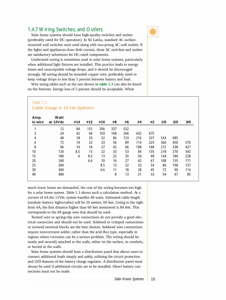
1.4.7 Wiring, Switches, and OutletsSolar home systems should have high-quality switches and outlets
(preferably rated for DC operation). In Sri Lanka, standard AC surface-mounted wall switches were used along with two-prong AC wall outlets. Ifthe lights and appliances draw little current, these AC switches and outletsare satisfactory substitutes for DC-rated components.
Undersized wiring is sometimes used in solar home systems, particularlywhen additional light fixtures are installed. This practice leads to energylosses and unacceptable voltage drops, and it should be discouragedstrongly. All wiring should be stranded copper wire, preferably sized tokeep voltage drops to less than 5 percent between battery and load.
Wire sizing tables such as the one shown in table 1.3 can also be foundon the Internet. Energy loss of 5 percent should be acceptable. When
much lower losses are demanded, the cost of the wiring becomes too highfor a solar home system. Table 1.3 shows such a calculation method. At acurrent of 4A the 12Vdc system handles 48 watts. Estimated cable length(module–battery–lights/radio) will be 20 meters, 60 feet. Going to the rightfrom 4A, the first distance higher than 60 feet mentioned is 84 feet. Thiscorresponds to the #8 gauge wire that should be used.
Twisted wire or spring-clip wire connections do not provide a good elec-trical connection and should not be used. Soldered or crimped connectionsor screwed terminal blocks are the best choices. Soldered wire connectionsrequire noncorrosive solder, rather than the acid-flux type, especially inregions where corrosion can be a serious problem. The wiring should beneatly and securely attached to the walls, either on the surface, in conduits,or buried in the walls.
Solar home systems should have a distribution panel that allows users toconnect additional loads simply and safely, utilizing the circuit protectionand LVD features of the battery charge regulator. A distribution panel mustalways be used if additional circuits are to be installed. Direct battery con-nections must not be made.
15Solar Home Systems
Table 1.3.Cable Gauge in 12 Vdc Systems
Amp. Wattin wire at 12Vdc #14 #12 #10 #8 #6 #4 #2 1/0 2/0 3/0
1 12 84 131 206 337 5322 24 42 66 103 168 266 432 6754 48 18 33 52 84 133 216 337 543 6856 72 14 22 33 56 89 114 225 360 450 5708 96 10 16 27 42 66 108 168 272 338 427
10 120 8.5 13 22 33 53 84 135 218 270 34215 180 6 8.5 13 22 35 56 90 144 180 22820 240 6.6 10 16 27 42 67 108 135 17125 300 8.5 13 22 33 54 86 108 13730 360 6.6 11 18 28 45 72 90 11440 480 8 13 21 33 54 67 85

1.4.8 InvertersIn larger solar home systems, DC-AC inverters can be used where cus-
tomers require AC electricity. It is not very common that users of systemssmaller than 100 Wp require inverters. The cost of an inverter and associ-ated energy losses recommend against its use in small systems. Severaltypes of inverters are available: square wave (the least expensive and leastefficient), modified square wave, and pure sine wave (the most expensiveand most efficient).
16Solar Home Systems

Chapter 2Lighting in Solar Home Systems
This chapter provides an introduction to the application of lighting insolar home systems. It consists of two sections. The first section dis-cusses the different types of lighting available. With the help of a
sample of actual measurements by ECN, some relevant characteristics oflighting are illustrated. The second section analyzes the operation of ballastsfor fluorescent. This includes a number of possible design modifications.
2.1 Design Considerations for LightsLighting is a basic necessity with a very high priority in households all
over the world. Many different means are available to meet these lightingneeds. When electricity first arrives in a village, lighting is by far the mostcommon application. Electric lamps have some major advantages over theirnonelectric counterparts. These advantages are increased lighting levels,higher lighting quality, greater ease of use, lower cost per unit of light out-put, no heat production, and very low fire hazard.
In conventional rural electrification with grid extension, there are fewincentives to apply energy-efficient lighting. Consumers lack the knowl-edge of alternatives and the usually low electricity tariffs do not provide astrong incentive to consider an optimum choice of lighting source.
However, when solar photovoltaics provide the electricity for rural light-ing, the situation is completely different. The high electricity cost per unitstimulates careful selection of the right type of lamp.
2.1.1 Types of LightingThere are four categories of lighting relevant for household solar PV systems:
General lighting (illumination of a whole room). Localized lighting (illumination of part of a room only). Local or task lighting (for example, illumination of a table). Orientation lighting (sufficient only to recognize shapes).
In relatively small rooms in which solar PV systems are used in develop-ing countries, the distinction between localized and local lighting becomesinsignificant. Both the luminaire and the lamp determine the possible useof the lighting, as in figures 2.1 and 2.2.
General lightingLights that are intended to be attached high up in a room are categorized
as general lighting. Most general lighting luminaires use fluorescent lampsand range in luminous flux from about 150 to 500 lumen. For the user it isrelevant to obtain the highest lumen output per watt of energy consump-tion [lumen per watt].
17Solar Home Systems
This paragraph is mainlyderived from a recentECN report,“Rural LightingServices: A Comparison of Lamps for DomesticLighting in DevelopingCountries.”

Localized and local lightingIn localized and local lighting, only a part of the room is lit. This can be
accomplished with small fluorescent tube types, or even better with com-pact fluorescent tubes. A reflector is usually included to concentrate thelight on the task area, and to prevent glare.
Orientation lightingDesigners of solar home systems often overlook the fact that many
people desire small orientation lights during the night. Very low light-ing levels are sufficient to recognize the shapes of furniture. For usersof PV systems, the power consumption of an orientation light is themost relevant factor. Small, 1-watt incandescent lights are very suit-able as a cost-effective orientation light. Lately, the development ofhigh-efficiency LED lamps has made significant progress. For bothlocalized and orientation lighting this can be a very suitable alterna-tive for the future, because of its high efficiency and long lifetime.
2.1.2 Luminous FluxLuminous flux is the technical term for the total light output of a
lamp in all directions as perceived by the human eye. The measure-ment unit is the lumen [lm], which takes into account that the eye ismore sensitive to some colors than to others.
The total amount of light emitted by a source, the so-called luminousflux, is one of the most important characteristics of a lamp. Luminousflux of lights in a test sample of 35 different lights measured by ECNranged from about 1 to 1,000 lumen for electric lights and fromabout 10 to 2,000 lumen for nonelectric lamps (Nieuwenhout,van de Rijt, and Wiggelinkhhuizen 1998). Figure 2.3 presentsan overview of the luminous flux measurements of all the lightsincluded in the test sample. As expected, the higher the powerof the lamp, the higher the light output.
Electric lights are far more efficient than nonelectric lights.For the household lights in the test sample it can be concludedthat at the same level of luminous flux, the energy consumptionof a nonelectric light is about 65 times higher than for an elec-tric light. There was no overlap in power between electric andnonelectric lights in this sample: the highest power electric lightis a 15-watt compact fluorescent lamp, while the lowest-powernonelectric light is small candle with an energy consumption of60 watts.1 If there had been an overlap in the power range, anelectric lamp would have a lumen output of about 2,000 timeshigher than the nonelectric lamps at the same wattage level.
Lights with a lumen output less than about 20 lumen are notmeant for general lighting, but usually function as orientation lights only.Most users prefer to have one or more orientation lights in their homes.
18Solar Home Systems
Figure 2.1A DC Light from Goldstar That Can Be Used for General or Localized Lighting
Figure 2.2Cluster LED Lamp from Steca
1 This is a comparison on the basis of energy input into the lightsource. When comparing primary energy inputs, the equivalent energyconsumption of the 15W PLET lamp will be in the order of about 50watts, the exact value depending on the fuel mix.

2.1.3 Luminous EfficacyConversion of fuels or electricity in visible light takes place as a result of
a number of different processes and under different conditions, resulting ina wide range of luminous efficacy.2
Figure 2.4 shows the luminous effica-cy (in lumens per watt of input power)for all lights in the test sample.
As figure 2.4 shows, electric lightsare much more efficient than nonelec-tric lights. Another interesting conclu-sion is that for both types of lights, therange in luminous efficacy levels is verywide. Electric lamps have luminousefficacy levels that range over a factorof 35, from 1.7 to 60 lumen per watt.The nonelectric lights in the samplerange from about 0.1 to 1.4 lumen perwatt. These wide ranges result from thedifferent technologies used and fromthe wide range in power of the selectedlamps.
Careful design of fluorescent lightballasts and luminaires is required toprevent unnecessary low light outputfrom lights in solar home systems.
2.1.4 IlluminanceThe amount of light that falls on a
surface is called the illuminance.3
Users are especially interested in havinglight sources provide sufficient illumi-nance on surface areas. For reading, aminimum illuminance of about 50 luxis required. For general lighting 20 to25 lux is sufficient, and for orientationlighting 10 lux or even lower can besufficient. Figure 2.5 shows illuminancelevels for light emitted in a downwarddirection (relevant for ceiling mounted,general lighting).
Figure 2.5 shows the illuminancelevels of the lights in the sample forwhich luminous intensity measure-ments are available in a downwarddirection. These typically are ceiling-
19Solar Home Systems
10,000
100
1,000
0.10.1 1 10 100 10,0001,000
1
10
Power [watt]
Lum
inou
s flu
x [lu
men
]
Figure 2.3Luminous Flux (lumen) and Energy Consumption (watt) for 35 Lights Measured by ECN
Electric Nonelectric
Electric Nonelectric
2 Luminous efficacy is the technical term for the efficiency of a light. Itis obtained by dividing the luminous flux by the power consumption. Theunit is lumen per watt [lm/W].3 The measurement unit is lux or lumen per square meter.
100
10
0.010.1 1 10 100 10,0001,000
0.1
1
Power consumption [watt]
Lum
inou
s ef
ficac
y [lu
men
/wat
t]
Figure 2.4Luminous Efficacy (lumen/watt) of All Lights Included in the Test Sample
Electric Nonelectric

mounted lights. Note that some of the lamps—for example, the solarlanterns—do not radiate downward. The vertical axis of figure 2.5 showsthe illuminous efficacy, that is the illuminance level per watt power con-sumption [lux/W].
Those who design lights for solarhome systems can reach the followingconclusions: Fluorescent tubes with areflector appear to be especially optimalin combining a high level of illuminancewith a high luminous efficacy. Adding areflector to the fluorescent-tube lumi-naire produces an approximate threefoldincrease in the efficiency, even thoughthe luminous flux of lights with a reflec-tor is about 10 to 20 percent lower dueto reflection losses. In the low powerrange the cluster LED is relatively veryefficient, but its illuminance is very low.This was one of the first prototypes ofthis new type of lighting and it will beimproved greatly within near future.
2.1.5 Measurements ofLuminous Flux
Usually, the luminous flux of electriclamps is measured in an inte-grating sphere (Ulbrightsphere, figure 2.6). An alternative approach is touse a goniophotometer inwhich the luminous intensityis measured in different direc-tions and integrated to obtainthe luminous flux of the lamp.Both methods require expen-sive equipment operated byspecialists.
Changes in the design offluorescent light inverters, aswill be discussed in the sec-ond part of this chapter, willchange the luminous flux andluminous efficacy of the light.Usually, the organizations thatmodify the equipment will notbe the same as those testingequipment for certification. When modifications are required, the luminousflux of the light usually is already known. This is an advantage for insti-
20Solar Home Systems
Illuminance [lux]
Figure 2.5Illuminance (lux) and Illuminous Efficacy (lux/watt) in a Horizontal Plane 1 Meter Below the Light Source
Illum
inan
ce e
ffica
cy [
lux/
wat
t]
00
10
2
4
6
8
10
12
14
20 40 60 8030 50 70
TL + reflectorBare TLIncandescentHalogenCluster-LEDCFL
Figure 2.6Ulbright Sphere for the Measurement of Luminous Flux

tutes involved in modification, since it is much easier to measure changesin luminous flux than to measure its absolute value. In the rest of this dis-cussion, it is assumed that the luminous efficacy of a light is known.
The following procedures lead to the determination of a luminous fluxchange, starting with a light with a known luminous flux: Measure the illuminance of the light in one direction [in lux] before
modifications (= Eb), using a lux meter (see next paragraph). Conduct modifications in the design. Measure the illuminance of the light in the same direction after
modifications (= Ea).The resulting luminous flux after modifications (Lua) can be calculated
from the luminous flux before modifications (Lub) using the following formula:
Lua = (Ea / Eb) x Lub
To check if the design modifications produce an increase in efficiency theluminous efficacy before and after the modification are compared. It hasimproved if
Lua/Pa > Lub/Pb
with Pa the DC input power after, and Pb before modification.The illuminance of the light [in lux] is measured with a lux meter. The
light is mounted in a fixed—and reproducible—position and distance fromthe lux meter. This distance between lamp and lux meter is not criticalsince it involves a relative measurement. But it is important that this dis-tance is exactly the same in both measurements. The light should be oper-ated at nominal voltage, and current and voltage should be measuredsimultaneously A closed box of wood or other sturdy material, is used tokeep stray light from influencing the measurement. The lamp is mountedabout one meter from the lux meter. Because the light output of fluorescentlamps is temperature dependent, the lamp should be allowed to stabilizefor about 20 minutes before a lux measurement is conducted. During thistime, the box should be left open to prevent heating of the box. The box isclosed during the lux measurements. Also, the ambient temperature of thetwo measurements should not differ by more than about 3ºC.
2.2 Fluorescent Lamp Inverters (FLIs)
2.2.1 IntroductionSmall local companies making fluorescent lamp inverters do not always
have enough highly educated technicians available. Young graduates inelectronics prefer to work for large organizations in the aircraft or comput-er industry instead of working in rural areas. Because of this, many localmanufacturers work with old circuit diagrams, sometimes based on poordesigns, mainly caused by the lack of knowledge and information.Companies know the complaints from the field: early blackening, and aluminous flux that degrades very quickly. It would be beneficial for smallproducers of solar home system equipment to obtain technical supportfrom a central research institute or university. These could provide techni-cal advice about improving existing designs.
21Solar Home Systems
Portions of this sectionmake use of the reportOptimal Design of DCLuminaires for Solar PVApplication, 1998, by HasnaJ. Khan, Rezwan Khan, andSalma Khatun,World Bank.

One of the weak components in the SHS is the fluorescent light. In manycases the tube starts blackening, or totally stops working, very soon afterinstallation. Another common problem in the field is fatal damage to lumi-naires while they are being transported to rural areas.
The most common causes of DC lamp failures in rural areas can beattributed to the following factors: Variation of operating conditions compared to the rated design
conditions. Inefficient design stemming from insufficient technical information on
DC lamps. Unavailability of reliable components for use in lamp construction. Misuse of lamps because the user has not received instructions. Insufficient quality control during manufacture of the lamp.
Not all of these issues are equally important for superior field perform-ance. However, these are some of the possible causes of problems that areassociated with the design of DC lamps.
2.2.2 Working Principle of a Fluorescent LightA fluorescent lamp (FL) is a high efficiency light source in which electri-
cal energy is converted into light without great loss of energy as heat.A schematic diagram of a
fluorescent lamp tube con-struction is shown in figure2.7. The glass tube is coat-ed with fluorescent(Phosphor) paint and filledwith mercury vapor.Tungsten filament connec-tions are provided at theends of the tube, which arethe sources of an arc dis-charge. Mercury can dis-solve the filament materialby forming amalgam, short-ening the life of the fila-ment. To prevent directcontact with mercury vapor,these filaments are coatedwith a layer of oxide.
A fluorescent lamp tube converts the electrical energy directly to electro-magnetic radiation, which emerges as visible light. When an electric cur-rent passes through the mercury vapor, the molecules absorb kinetic energyand are ionized When an ionized atom recombines with an electron, andthe electron drops back to its original energy level, the mercury atom radi-ates ultraviolet light. Ultraviolet light is not visible to the human eye. So afluorescent material is painted on the inner surface of the tube that con-verts the ultraviolet radiation into visible light.
AC voltage is needed, but at what frequency? Grid-connected fluorescentlamps work on 50Hz. Ballasts for solar home systems work on 20kHz or
22Solar Home Systems
Electrode
Phosphor coating
Visible light
Ultraviolet light
Electric arcMercury atom
Figure 2.7Schematic Diagram of a Fluorescent Tube Light

higher. Within SHS the power supply is a 12Vdc battery. The electronicsinside the lamp fixture have to be as small as possible. A transformer isneeded, but the size of the transformer can be smaller when the frequencyis higher. At higher frequencies the efficiency of the FL is higher. At 20kHzthis efficiency is 15–20 percent higher that at a frequency of 50Hz. On theother hand, when the frequency is too high, the lumen output willdecrease, and the internal resistance of the tube will be higher, so the volt-age at the terminals will also rise.
With the onset of ionization, the resistance of the tube drops dramatical-ly and current rushes through the circuit. This nonlinear dependence ofresistance of the tube on the current flow makes the operation of the fluo-rescent tube a unique component of the ballast circuit.
There are two techniques for initiating ionization inside the tube. Theyare called “hot start” and “cold start.” In case of hot start, the filaments areinitially heated by passing a strong current through the filaments only. Thefilaments have two functions: they are the electrodes for providing the elec-trons and the filaments for preheating. Heating of the filaments increasesthe emission of electrons from the filaments, which makes ionization easier.During a cold start the applied voltage across the tube terminal has to behigher than with a hot start. From the user point of view, the hot startrequires some time (only a few seconds) to start up the lamp, but the coldstart technique can start the lamp within a few milliseconds, effectivelymaking it almost instantaneous. For more about preheating, see Section2.2.8, Effect of Filament Preheating.
2.2.3 Blackening of the Fluorescent LampDegradation of fluorescent tubes starts when the ends become black, and
this is the main reason that fluorescent lamps fail prematurely. When atube light is switched ON, it does not remain on all the time. During eachhalf cycle, it remains ON as long as the voltage across the tube is sufficientto keep the gas inside the tube ionized. When the AC voltage passesthrough its zero crossing, the light goes OFF. It comes ON once again whenthe voltage magnitude rises in the next half cycle.
When the light is ON, a number of things happen inside the tube. First,the gas molecules become ionized and start moving toward the ends, dueto the effect of the electric field. Hence, the ionized molecules becomephysically separated as the positively charged ions and electrons move inopposite directions toward the negative and positive potential ends of thetube respectively. When the voltage wave goes through the zero crossing,these separated ions start their reverse journey to recombine and, if givenenough time, almost all of them will reach the original energy level. Undersuch a circumstance, a significantly large voltage will be required across thelamp tube terminal to start it in the next half cycle. It is frequentlyobserved in the current and voltage wave shapes of the tube lights operat-ing at 50/60Hz that the current starts to flow after zero crossing when alarge ionizing voltage is build up across the tube light. On the other hand,if the frequency is high, there is not enough time for the electrons in themercury atoms to fall back in their original energy level. The magnitude ofcurrent flowing through the tube light represents the actual number of
23Solar Home Systems

molecules/atoms ionized. A lower magnitude of current means fewer ion-ized molecules and the voltage level required to restart the lamp after eachzero crossing becomes larger. When the frequency is too high, the efficien-cy goes down and the terminal voltage will rise dramatically because of atoo-high internal resistance of the tube. Fewer atoms can be ionized,because there is no full recombination. Higher terminal voltage causes theions to bombard the filament with a higher kinetic energy and the oxide coatingon the filament gets damaged at a faster rate.
Four general causes for premature failure of DC lamps can be defined:1. Damage of the filaments because of overvoltage across the tube,
or end blackening.High voltage at the tube terminal due to low DC input voltage:
Lower input DC voltage results in a lower magnitude of currentin the tube light. Because its internal resistance is now higher(fewer molecules are ionized), the tube light terminal voltage isautomatically raised. Hence, the oxide coating is damaged earlierthan expected and mercury deposits on the filament causing cor-rosion by amalgamation. Fluid amalgam is sprayed from the fila-ment by the effect of the AC potentials. The sprayed amalgamshows up in the form of blackening of the tube ends. Blackening ofthe ends has a twofold effect: The amount of mercury vapor left inside the tube to form the
ions is reduced as some of the mercury forms amalgam with thefilament material.
A shortage of the mercury vapor reduces the current flow andthe terminal voltage increases as a consequent. This increase interminal voltage enhances the rate of damage to the filament.Therefore, once blackening of the tube starts, the process ofblackening continues even with the correct voltage.
High voltage at the tube terminal due to high DC input voltage:This is a secondary cause of high voltage appearance at the tubeterminal. With increasing input DC voltage, spikes may appear inthe voltage across the lamp tube, because the transformerbecomes saturated due to an incorrect number of turns in theprimary winding, particularly if the number of windings is low.More of the transformer calculations can be found in Section2.2.10, Inductance Calculation of the Transformer Coil.
Why blackening frequently occurs at one end of a tube:Blackening takes place more quickly on one end of the tubebecause the ballast circuit generates an asymmetric voltage waveand high voltage spikes are generated during one of the halfcycles. Usually, positive ions (mercury molecules) have a highermomentum than the electrons and damage is done to the nega-tive potential terminal. In the case of a symmetric wave shape,the damage due to overvoltage is shared equally by both the fila-ments. If the wave shape is asymmetric, one of the filaments isdamaged more than the other one is, and the lifetime of the lampis drastically reduced.
24Solar Home Systems
2. Contamination of the gas inside the tube.Mercury vapor inside the tube may be contaminated if oxygenremains inside the tube due to some fault in the manufacturingprocess or due to leakage. In both cases, oxygen in the air reacts withmercury to form oxide and the life of the tube light is drasticallyshortened. Contamination of the mercury will require a higher voltageto ionize the gas inside the tube and this higher voltage will graduallydamage the filament as explained before. This is not a major factor inlamp failure, although poor quality gas mixture is known to produceless light and reduce the tube life.
3. Damage of the filament because of excessive current flow while preheating.The filament of the tube light is designed to preheat the gas inside thetube for a short while just after start-up. Excessive current flow or alonger period of preheating can result in filament overheating. The fil-ament is damaged when the filament and its oxide layer are burnedmuch earlier than the expected lifetime of the tube.
4. Damage of the filaments because of high current spikes.In some situations the filament can be damaged even without anexcessive current if the wave shape of the current contains largespikes. Current spikes of short duration on the secondary side of thetransformer cannot be detected in the input current consumed by theballast circuit. But these short current-spikes flow mainly through thepreheating capacitor and on through the filaments, as discussed inSection 2.2.8, Effect of Filament Preheating. Hence excessive heatingwill occur at the filaments. Under such a condition, a given lamp cur-rent will produce more heat and less illumination. Hence, it is impor-tant to design the ballast circuit to avoid high spikes of current.
General recommendations for an optimized design for DC lamps: The generated wave shape should be symmetrical in both half cycles. There should be no voltage spikes on the output wave shape at the tube
terminal. (low crest factor).4
The ballast normally should be designed to operate the lamp tube at itsrated power, otherwise blackening will occur very quickly in case ofoverdesign, or the ballast is overloaded for the unit it supports.Possible remedies for blackening of the tubes:It is clear from the above discussion that rated current should be main-
tained to avoid blackening of the tube lights. This can be achieved as follows: By keeping the input DC voltage constant, or By keeping the voltage across the lamp constant.
Using proper electronic circuitry, it is possible to keep the input DC volt-age constant even if the DC battery voltage is reduced (Zener diode or volt-age stabilizer). If the voltage control is to be applied at the tube light termi-nals, a variable frequency output voltage is needed. Normally, there is animpedance connected in series with the tube light to control the currentthrough the lamp when the light is ON. If the series impedance is aninductor (usually the leakage inductance of the output transformer), the
25Solar Home Systems
4 The crest factor is defined as the ratio between the peak and the rootmean square (RMS) value of the voltage or the current.

frequency should be reduced to reduce the voltage drop across the induc-tance. If the series impedance is a capacitance, frequency should beincreased to get a similar effect. Changing the frequency is not possiblewith the conventional self-oscillating circuits. It ispossible to obtain a vari-able frequency output ifthe oscillator circuit uses avoltage control oscillator(VCO). A good electronicballast circuit designensures the long life of atube light.
2.2.4 LampInverters with Oneor Two Transistors
As previously stated, asymmetric wave shape onthe lamp terminals con-tributes to a longer lifetime.Some of the inverters testedby ECN were based on aone-transistor design. Twoof the resulting waveformsare shown in figure 2.8.The upper diagram showsan inverter with a substan-tially asymmetric crest fac-tor of almost 4.5. At thestart of each cycle, a veryhigh voltage peak is sup-plied at its terminals. Thiscauses early blackening onone side of the tube.Because the electronics arenot built symmetrically, thetube will not light up dur-ing the negative half of thewave. There is current flowing, but the voltage was not high enough to startthe ionizing process. The lamp is OFF during this half cycle.
The most common design of high-frequency inverters uses a balancedcircuit with a resistor, inductor, and capacity (LRC) circle to drive two tran-sistors in a sine wave. Without a tube the output is a sine wave with anamplitude of about 600V. As soon as the tube (with its unique resistancecharacteristic) is added, it is a problem to maintain that “ideal” sine wave(figure 2.9). The inverter below gives an example of a two-transistorinverter, which creates a more or less symmetrical waveform.
26Solar Home Systems
120
160
80
40
0
–20
–40(a)
(b)
1.5
2.0
1.0
0.5
0
–0.5
–1.0
Voltage (V)
Figure 2.8Two Examples of a Waveform of a One-Transistor DC-FLI
Current (A)
40
80
0
=20
–40
–80
–120
–160
–200
0.4
0.8
0
=0.4
–0.8
–1.2
–1.6
–2.0
–2.4
Voltage (V) Current (A)

A remarkable factor is that the basic shape of the wave does not matter.There is no difference in lifetime with a square or a sine wave inverter, aslong as the basic demandsare regarded: low crestfactor, symmetrical waveshape, and so forth.
During testing, thewaveform should bechecked in detail on thezero-crossings on the pri-mary side, on the collec-tors of the transistors. Ifthese zero-crossings have“overlap,” there will beunnecessary energy lossand even voltage and cur-rent peaks. During theoverlap time the two tran-sistors are both partiallyconducting. A short cir-cuit is created via thetransformer. Figure 2.10illustrates this situation.The moment that a tran-sistor starts its function at its half cycle, the other transistorhas to be totally closed.
On the other hand, if the time t is too long, the luminousefficacy will be reduced unnecessarily. Because of the circuitwith an inductance (L) and capacitor (C) (LC circuit) at thesecondary side of the transformer, the effect of this is diffi-cult to detect in the tubes terminal voltage wave.
2.2.5 Different Transistor Set-UpsFirst, two basic principles will be explained, and then
four different samples will be discussed. These four types ofballast represent four degrees of performance; each wasmanufactured in a different developing country.
In general, two types of ballasts can be identified: thechopper circuit and the push-pull configuration. The chop-per design is the less expensive of the two. Its basic diagramis shown in figure 2.11.
When the system is switched ON, a DC current willcharge capacitor C2 via the primary winding of the trans-former. As soon as the anode of the capacitor is higher than1.4V (Vbe of the transistor + voltage drop D1) the transistorstarts conducting. C2 discharges via T1. When it is discharged the transis-tor closes again, so C2 can be charged. The charging is “chopped off” whenit reaches a certain level. This creates an AC current in the primary side ofthe transformer during the “chop.” The result is an asymmetric output
27Solar Home Systems
80
40
0
–40
–80
–120
2.0
1.0
0
–1.0
–2.0
–3.0
Voltage (V)
Figure 2.9Waveform of a Two-Transistor DC-FLI
Current (A)
V
T2
T1 dtt
Figure 2.10Well-Trimmed Transistor Takeover

signal that functions in just one half of the cycle. Most of the time there issome switching signal during the other half cycle, but this is not enough toionize the lamp. During this half cycle the lamp will be off. The RC (circuitwith resistance and capaci-ty) time of R1/C2 and theinductance of the primarywinding define the fre-quency of this system.
Diode D2 is the polarityprotection at the DC input.When T1 is conducting,the DC input is in shortcircuit. That means a lot ofenergy loss and a lot ofheat. C1 is needed in orderto avoid the DC short cir-cuit. It passes only on ACcurrent, resulting in thedischarge energy from C2.
The second set-up is thepush-pull configuration,shown in figure 2.12.
Again, D1 is the polarityprotection. Now the pri-mary windings create asymmetric magnetic field inthe core of the transformer.One half cycle T1 is mak-ing the field, the other halfcycle T2 reverses this field.The feedback winding isvery important. This wind-ing forces T2 to close whenT1 is conducting and viceversa. So it actually isresponsible for the oscilla-tion. Without this, the twotransistors both would beconducting, forming a short circuit via the primary windings.
Transistors are never exactly the same. When this system is switchedON, the fastest transistor will conduct first. This creates a voltage differenceat the feedback winding, which closes the slower transistor until the fieldin the core is totally built up. At that moment there is no voltage difference(which forces the slower transistor to close) at the feedback winding, so theslower transistor takes it over by reversing the field, while the faster transis-tor is now forced to close by the feedback winding.
28Solar Home Systems
V+
D2Transformer
C2
10n
R1
D1
T1
Lamp
C1
V–
Figure 2.11The Chopper Design
D1
Transformer
T1
T2
R1 R2
Lamp
V+
Figure 2.12The Push-Pull Configuration
V–

The result is a symmetrical wave shape at the lamp terminal. Duringboth half cycles there is enough voltage and current to start the ionizationprocess.
Four Chopper Design Set-upsThe following text looks
at four different set-ups forthe chopper design.
Set-up 1 (figure 2.13):In this circuit no atten-tion was paid to optimiz-ing the circuit. The lamphad a very early stage ofblackening and the effi-ciency is too low.
Rated operating condition:Input DC voltage: 12VOutput power: 8W
The primary weaknessesin the circuit of design 1are as follows: No prevention for voltage and current peaks at the lamp terminal. Bad crest factor. Very asymmetric wave shape. Heat-producing transistor needs to be cooled.
Dangerous point: No DC polarity protection. There is an electrolytic capacitor (elco) added
at the input (2,200µF). This is polarity sensitive. The elco can be dam-aged after a wrong connection is made, but it is not necessary in the firstplace. It is connected in parallel with the battery, so it functions like “avery small battery next to a battery.” Its value is so high that it is not asufficient filter for high frequencies.The second chopper design is related to this design, so there are no fur-
ther comments.Set-up 2 (figure 2.14): This lamp was designed with a diffuser for
area lighting, with little attention to circuit performance optimization.Hence, the circuit design was not efficient.
Rated operating condition:Input DC voltage: 12VOutput power: 8WThe principle of this design is about the same as design 1. The main
differences are as follows: Polarity protection on DC input. Frequency generation at the collector in stead of at the base
(.22µF / 180). The oscillation (470) thus needs to be activated. Two transistors are parallel.
29Solar Home Systems
D1
T1 R1
C2
10n
C10.01µF+C2
2,200µF
Transformer
Lamp
V+
Figure 2.13Diagram of the Ballast Circuit: Example Set-up 1
V–

Primary capacitor (.01µF).Main weaknesses of this design are as follows:
Two transistors have been used in parallel, apparently to share the loadcurrent. But it is not advisable to use parallel operation of the bipolarjunction transistors (BJTs) since they may not share the load equally. Dueto the parallel connection of the transistors in this circuit, one of thetransistors carries the full load and the temperature of the transistor inopen-air conditions can reach 100oC, which is extremely high. This maycause early damage of the transistors due to overheating and at the sametime it indicates excessive power loss.
There is a high-power 470-ohm resistance connected from the collectorto the base of the transistors. This resistance is responsible for the initial-ization of oscillation. As it is connected from the collector to the base,the resistance is effectively dissipating four times that required by a gooddesign. An easy way to improve this is to replace this resistance by ahigher value of resistance (about IK ohm) from the 12V supply to thebase. A power rating of just 0.25W should be enough.
As far as the blackening of the tube light ends are concerned, it has beenobserved that the wave shapes become very distorted with voltage spikesat the output when the input DC voltage is reduced. During the prelimi-nary tests, with 7V DC input, one end of the tube became black afterrunning for just 25 hours.Set-up 3 (figure 2.15): The performance of this set-up was expected
to be better than set-up 2. This design qualified other standards andthe manufacturer optimized the circuit performance.
Rated operating conditions:Input DC voltage: 12VOutput power: 8WThis push-pull-configured design was found to be well designed circuit
with very small loss in the transistors, as evidenced by the low tempera-
30Solar Home Systems
C10.01µF
R1470
R2180
0.22µF
C2D1
Figure 2.14Diagram of the Ballast Circuit: Example Set-up 2
Transformer
T1 T2
Lamp
V–
V+

ture, which was nearly equal to the room temperature. The circuit usedtwo transistors firing for each half cycle, producing a symmetric waveshape. Control over the wave shape was much better and the wave shapedistortion was much less with reduced voltage. Lumen per watt of thelamp was found to be quite high, reflecting the small amount of loss occur-ring in the circuit. After 30 hours of running at 7V DC input, no apparentblackening of the tube was observed. However, in later tests, blackening
was noticed after 137 hours of operation under this severe condition.Set-up 4 (figure 2.16): This lamp had the best design in terms of
efficiency (luminous efficacy) and ballast circuit performance. Thisdesign was known to meet stringent quality standards.
Rated operating condition:Input DC voltage: 12 VRated power: 8 WThis proved to be the most efficient lamp design under consideration.
The primary characteristics are as follows: Constant voltage is maintained (Zener Z1) on input. The wave shape is symmetric. The capacitor preheats. There is little distortion.
The following must be noted: Uniform performance is seen over the acceptable battery voltage range.
Battery voltage in a solar home system varies from 14V to 11V depend-ing on the depth of charging and discharging. Hence an ideal DC lampshould give uniform output over this voltage range. The usual DC lampsavailable worldwide give higher power output at higher battery voltage.To keep the power output uniform, an additional circuit may be neededwhich would marginally add to the cost of the DC lamps.
The frequency range over which most of the DC lamps operate is20–30 kHz. This frequency range is chosen to give an optimum size of
31Solar Home Systems
C2
0.0022µF
C1
820820
0.22µF
Figure 2.15Diagram of the Ballast Circuit: Example Set-up 3
D1
Transformer
T1
L1
T2
R1 R2
Lamp
V+
V–

the ballast and to keep the switching loss of the transistors withinacceptable limits. A higher frequency range would reduce the size of theballast but increases the transistor switching loss. The leakage inductance(L) of the transformer has an impedance (L) that is proportional to thefrequency. Any capacitor (C) used in the circuit has an impedance (1/C)inversely proportional to the frequency. Hence changing any L or C altersthe frequency and the overall impedance of the circuit, so correspond-ingly modifies the power input to the lamp.
Low battery voltage has the following effects: Voltage at the lamp terminalscan be low if the battery voltage becomes low or the line loss is too high.Low voltage at the lamp terminals reduces current flow in the lamp. Asthe impedance of the lamp is highly nonlinear and inversely related tothe actual current flow through the lamp, its impedance increases withthe decreasing current flow causing high voltage spikes in the voltagewave shape. These spikes cause high-energy ions to bombard the fila-ments and may cause irreversible damage resulting in blackening of thetube ends.
The effect of the voltage and current wave shape is shown in the presence ofhigh-voltage spikes in the voltage waveform: This is the main reason for theblackening of the tube ends. The actual shape of the voltage wave (con-taining no spikes) does not affect the speed of the blackening process.High current spikes do not cause blackening if the spikes are not presentin the voltage wave shape. It often happens that the current and voltagewaves contain DC offsets, especially those circuits without push-pull cir-cuit configuration. These DC offsets are observed in the unequal peakvalues of the wave during two half cycles but cause no problem if spikesare not generated.
32Solar Home Systems
100 µF
C1680 680
R1 R2
L1
Z10.0047µF
C2
D1
Figure 2.16Diagram of the Ballast Circuit: Example Set-up 4
Transformer
T1
T2
Lamp
V+
V–

2.2.6 Polarity ProtectionNormally, DC lighting is mounted on a wall or fixed to the ceiling for
better access to the user. If people who buy and install new lights them-selves do not have a technical background, they could easily make a mis-take in the connection. This is one of the main reasons why polarity pro-tection for DC lighting is necessary.
Usually an input diode is used for polarity protection. These componentshave a voltage drop of about 0.6V. For a 12V DC lamp with a rated powerof 8W, this means 0.4W energy loss.
It is also possible to use a “polyswitch,”as shown in figure 2.17. In normal usethese have a voltage drop of about 0.4V,resulting in efficiency improvement of 3.3percent toward the 12Vdc input. A poly-switch is current-sensitive. When the cur-rent increases, the polyswitch resistanceincreases dramatically, so that the currentis limited to a minimum. If the polarity ofthe ballast is wrong and there is no protec-tion integrated, the reverse currentbecomes so large that components aredamaged. In the polyswitch, the current isreduced to a safe level so that no compo-nents will be overstressed. The lamp itself,however, will not be lit, because none ofthe transistors is in conduction, so no ACvoltage is generated.
A third option for polarity protection is the use of a MOSFET, as shown in figure 2.18.
A cooled power MOSFET is unnecessaryin this case, because the current stays atabout 1A for an 8- to 10W fluorescentlamp. Depending on the internal conduct-ing resistance, the voltage drop can bereduced to approximately 0.1 or 0.2 V.However, the price of a MOSFET is rela-tively high compared to that of a diode.
2.2.7 Field-Effect Transistor (FET) versus TransistorUntil now, most fluorescent lamp inverters (FLIs) have used transistors.
Transistors were invented a long time ago and were readily available whenthe first fluorescent lamp inverters were designed. Power MOSFETs wererelatively expensive. Nowadays field-effect transistors (FETs) have becomecheaper, and when used in FLIs they have certain advantages. For example: A lessened drop in voltage produces less energy loss. Use of an internal freewalk diode causes less of a voltage peak when
switching from OFF to ON.
33Solar Home Systems
R
Working areaI
Figure 2.17Polyswitch Characteristics
Figure 2.18The Use of a MOSFET for Polarity Protection
MOSFET N
V+
V–
+ballast
–ballast

There is also one important disadvantage associated with FET use.Because the input current of a FET is negligible, an oscillation with only afew components cannot be established. An independent steering mecha-nism for the FET must be created.
When using MOSFETs, the steering needs to be different. You cannotjust simply exchange transistors by FETs. Because no direct oscillation canbe created, a signal-wave oscillator will have to be added. A simple squarewave is enough. If the frequency and the transformer-inductance are welltrimmed, the output can be a good sine wave. Because of the freewalkdiodes in the MOSFETs, fewer voltage and current peaks will occur. Whenthese do occur, the same measures can be taken as for transistor-inverters.Also, a good input filter is needed between the main system and the highfrequency part, because of the electromagnetic (EMC) effects on the systemwires. The main system (without filter and other precautions) is shown infigure 2.19.
The Hefei University ofTechnology in China creat-ed an identical inverterwith such a perfect sinewave on the lamp—show-ing a crest factor of about1.57—that no voltage orcurrent spikes could bedetected. The disadvantageof the design was that itused a relatively expensivePWM IC for the steeringpart. It might be interestingto do some research on aFET-controlled ballast withan analog oscillation circuit.
2.2.8 Effect of Filament PreheatingPreheating the filaments helps to ionize the gas inside the tube and bring
the lamp to its full glow more easily with less applied voltage. It is impor-tant to understand the actual mechanism of starting a DC lamp to ensurelonger life of the lamp. When a lamp is switched ON, the lamp starts toglow immediately (without any noticeable time delay). It does not come tofull glow instantly, but suddenly increases 4–5 seconds after the lamp isswitched ON. During this period, the gas inside the tube is not completelyionized and the voltage across the tube remains high. The less time that isrequired to attain full glow, the better it is for the lamp. Preheating mini-mizes this start-up time and many of the manufacturers of DC lamp ballastcircuits prefer filament preheating to ensure longer life. Figure 2.20 showsthe configuration for filament preheating from the secondary side of thetransformer. Four pins are connected to the tube end for this configuration.
Preheating of the filaments is simple and inexpensive. Two additionalwindings in the transformers can be provided for the filament supplies andcan be connected at the ends of the tube. Although this system does not
34Solar Home Systems
MOSFET N
MOSFET N
20 kHz
Transformer
Lamp
Figure 2.19Example of MOSFET Use in FLI
V+
V–

cost much money, it will drain power all the time and the overall efficiency ofthe lamp will be reduced. However, the loss of energy is compensated by thelonger life of the lamps. Hence, this tradeoff depends on the cost of energycompared to the cost of the lamp itself. In solar home systems the cost ofenergy is very high, and this leads to many designs that use a cold start.
Another option for preheating, which does not make straight use of anextra winding at the transformer, is connecting acapacitor between the (not connected) pins ofboth filaments as shown in figure 2.21. The start-ing sequence for this type of FLI can be dividedinto three phases, as shown in figure 2.22. A phase where the voltage is being increased. The
gas inside the tube is not yet ionized, so itsinternal resistance is very high. The voltageover the tube is being built up to 500 or 600 V.Because of the high internal resistance of thetube, this AC current will flow through the par-allel capacitor. In this phase the current resultsin the heating of the filaments.
The ionization phase. When the voltage is highenough, the first ionization will take place. Theinternal resistance of the tube will drop drasti-cally. From now on the main current will flowthrough the tube.
The steady state of the ballast and lamp. Duringthis period the voltage will stay at approxi-mately 60V. While the lamp is ON, the currentwill flow through the tube because of its lowresistance. During the zero crossings, dI/dt ishigh, and the lamp is off, so there is a highresistance. During this very short time,current will flow through the capaci-tor. Because this is only a very shortperiod, it will not contribute to effec-tive heating because the filaments arestill hot from the last cycle.When the filament is being preheated,
its temperature rises and electrons canleave the filament more easily. Free elec-trons gather around the filament until thevoltage is high enough to ionize the gas.Due to the higher number of free elec-trons, this ionization can start at a lowervoltage.
The important thing is that the overallefficiency is not reduced. Only one extra capacitor is required, so it is avery cheap and energy-saving method of preheating. The parallel capacitoris often used in FLIs of all price classes.
35Solar Home Systems
Lo
Lamp
Co
Transformer
Figure 2.20Configuration for Filament Preheating
Lamp
CTransformer
Figure 2.21Filament Preheating with Parallel Capacitor

2.2.9 Critical Components and Component QualityFollowing the basic alternative ballast circuit designs given in the previ-
ous section, this section discusses the role of the individual components inthe overall performance and efficiency of the ballast.
The transistor(s)The transistor is one of the critical components to
determine the frequency of operation of the ballast cir-cuit. A good choice of transistors is very important in theballast circuit, because most critical components of theballast are frequency dependent. The frequency of opera-tion should be chosen considering the frequencyresponse of the transistor. For an efficient operation ofthe transistor, the operating frequency should be chosento be less than l/hFE () times the ultimate frequency limitfT , where hFE is the frequency response as a function ofthe gain factor hFE (). Mathematically speaking, theoperating frequency f should be set according to
f< fT / hFEIf the operating frequency is higher than acceptable,
the junction capacitance becomes prominent, whichmakes switching the transistor ON and OFF slower.When the operating frequency is higher than the fre-quency mentioned above, junction capacitance slows thetransition-switching rate. This causes extra power lossinside the transistor. This situation is shown in figure2.23 (a) and (b). The base voltage VB has a square waveshape in (a), but the switching function causes the collector voltage Vc, to be distorted with power loss, as shown in (b).
For a transistor to operate efficiently, it shouldeither operate in the saturation or in the cutoffregion. Power dissipation inside the transistor is theproduct of transistor voltage drop and transistor cur-rent. When the transistor is switched ON, it goes tosaturation and the voltage across the transistorbecomes very low (on the order of 0.2V), althoughthe current may be high. The product of the voltageand current is low due to low saturation voltage.When the transistor is switched OFF during theother half cycle, it must be able to handle the fullvoltage (open circuit) without breaking through.Hence the product of current and voltage is still veryclose to zero. Such an operation produces very littlepower loss and the transistor keeps cool, ensuringlonger life and less possibility of failure.
36Solar Home Systems
Figure 2.22Starting Sequence of an FLI
Increasing voltage
Steadystate
Arc strike
Vb
t(a)
(b)
Figure 2.23Power Loss during Transistor Switching
Vc
t

The transformerThe transformer is the most critical component in the design of the elec-
tronic ballast circuit. DC lamps normally are operated in the frequencyrange of 20–30kHz. Because normal iron cores lose energy at these fre-quencies, ferrite cores are used. The voltage induced in a coil is given byFaraday’s law of electromagnetic induction mathematically given by Nd/dt,where N is the number of windings, is the flux inside the core and t is thetime. If the operating frequency is high, d/dt is high. This means smalleramounts of flux can generate the required voltage and the actual size of thecore can be reduced correspondingly. As discussed earlier, there are a num-ber of physical constraints such as the switching loss and the price of thetransistors that limit the upper frequency limit.
The transformer plays two very important roles in the successful opera-tion of the lamp: Starting condition: generating high voltage during starting. Running condition: producing the right value of inductance to prevent
excess current to the lamp tube. It is very useful to experiment with thetransformer to verify the effects.A discussion of these effects follows:Starting condition: Ideally, the ratio in the number of windings of the
transformer should be such that the voltage generated at the lamp tubeterminal is high enough to initiate ionization of the gas. During this time,resistance of the gas is very high and the current through the tube is low,making the inductive voltage drop Ldi/dt and the inductance small.Hence, the full voltage generated in the coil appears across the tube andthe gas is ionized.
Running condition: As the gas ionization process increases, current flowalso increases simultaneously and the voltage drop across the inductanceincreases, reducing the voltage across the lamp. When the lamp comes tofull glow, the voltage drop across the leakage inductance should have avalue so that correct voltage appears across the tube.
In most cases, it is difficult to satisfy both the starting and running con-ditions. In circuits without a capacitor across the primary side of the trans-former—connected to the collector of the transistor(s)—current starts flow-ing in the primary coil when the transistor is ON. After half cycle, the tran-sistor is suddenly switched OFF, which tends to chop the current OFFinstantly. This mean a very high value of di/dt, which correspondinglyinduces very high voltage at the lamp ends and helps the lamp to starteven when there is a much lower voltage at the primary side of the trans-former. Although this design may be suitable for starting the lamps, it has anumber of drawbacks.
First, it makes the lamp glow at a much lower voltage, and the lamp maynever attain its full glow. Second, even if the lamp comes to its full glow, itmay take longer. During the period of this partial glow, the ionization ofthe gas in the tube remains incomplete. The impedance of the lampremains much higher than that of the normal operation and high voltageremains across the tube. Hence, blackening of the tube ends take placemuch earlier.
37Solar Home Systems

One way to avoid such a damaging phenomenon is to prevent low-volt-age starting of the lamps. A lamp should start only when the input DCvoltage is high enough to generate full glow. The solution lies with theaddition of the capacitor in the circuit across the transformer on the primary side.
The capacitor and inductor on the primary side of the transformer The capacitor across the primary winding of the transformer is an impor-
tant component for ensuring the long life of the tube light and preventingend blackening. The two basic circuitconfigurations using capacitors acrossthe primary winding are shown in figure 2.24.
When there is no capacitor acrossthe primary side of the transformer,switching the transistor OFF from theON state would generate high-voltagespikes. As discussed earlier, this wouldinitiate ionization inside the tube pre-maturely even when the battery volt-age is insufficient to produce sustain-able full glow of the lamp. To elimi-nate this problem, a capacitor is con-nected in parallel with the primarywindings of the transformer. When thetransistor is switched OFF from theON state, the current through theinductance is not interrupted, as thereis a path for current flow through thecapacitor. This reduces the voltagespikes. It is possible to design thetransformer and choose the value ofthe capacitor in such a way that thelamp will be ON only when the DCbattery voltage is at the correct level.
Addition of such a capacitor would,however, cause current spikes throughthe transistor whenever the transistoris switched ON from the OFF posi-tion. This will increase power loss inthe transistor, causing overheating andreducing the overall efficiency. Inextreme cases, the transistor may evenget damaged. A small inductance inseries would reduce any such currentspike. The position of the inductancein the circuit is shown in figure 2.25.
38Solar Home Systems
Ci
Figure 2.24Capacitor across Primary Winding of Transformer
(a) Chopper circuit
(b) Push-pull circuit
Lamp
Transformer
Transformer
Ci
Ci
T1
T2
Lamp

The capacitor and inductor in the secondary side of the transformer (in series with the tube)
Role of the series capacitor during running: When a capacitor is added inparallel with the primary winding of the transformer as discussed earlier,the voltage spikes generated due to abrupt switchingOFF of the transistors are suppressed. This causesdifficulty in starting the lamp in the absence of thehigh voltage spikes. So the transformer windings ratiois increased to have enough voltage at the output toinitiate ionization. However, such increased voltagecauses excessive current flow through the tube lightunder steady state (running) conditions and the lampmay get damaged. For this reason, a capacitor isadded in series with the lamp to limit current in thecircuit as shown in figure 2.26.
Role of the series capacitor during starting: It is inter-esting to observe that this series capacitor helps sig-nificantly in improving the overall performance of thelamp. It has already been mentioned that the lamp isa highly nonlinear device with its resistance varyingwith applied voltage by a large margin. Every halfcycle, the current through the lamp goes through azero crossing and the lamp goes OFF momentarily. Itwill not start to glow again in the next half cycle untila significant voltage is reached. During this OFF peri-od, the resistance of the tube remains very high.Once the capacitor is charged from one of the halfcycles, it adds to the voltage of the next cycle untilthe lamp glows. This means the lamp always sees ahigher voltage, which is the sum of the capacitor volt-age from the previous cycle and the voltage from thetransformer. So the lamp starts much earlier each halfthan it would without a series capacitor.
Role of the inductor in series with capacitor: The addi-tion of the capacitor in series with the lamp has a dis-advantage. When the lamp starts conduction afterzero crossing in each half cycle, the resistance of thelamp suddenly decreases, causing the capacitor todischarge very rapidly and resulting in high currentspikes. Sustained current spikes of high magnitudewould generate more heat at the filaments and reducethe overall efficiency of the lamp. The filaments mayget damaged in the long run. However, the adverseeffects of the current spikes are much less in comparison with the voltagespikes. Current spikes through the lamps can be suppressed by adding asmall inductor.
The final form of the secondary side of the transformer circuit is shownin figure 2.26. It shows the configuration with a capacitor and an inductorin series with the tube.
39Solar Home Systems
Ci
(a) Chopper circuit
(b) Push-pull circuit
Figure 2.25Inductor in Series with Primary Side of the Transformer
Ci
Ci
T1
T2

Tolerances of componentsThis chapter illustrates some specific types of variation in the perform-
ance of DC lamps caused by external events, such as the quality of elec-tronics components and spare parts used in manufacturing and mainte-nance. The results reflect the significance of quality controland its absence in the markets of the developing countries.The objective is as follows: To obtain information about the variation of input current
consumption levels, which will affect the overall perform-ance of the lamps.
To demonstrate the variation of the actual from the ratedvalues for inductance, resistance, and transformer coil typ-ically used in the DC lamps.
Performance of DC lamp ballast with different tubesFluorescent tubes used in DC lamps are typically pur-
chased on the open market, where various brands are avail-able at different prices. Selection of the tube is strongly influ-enced by the price and past experience of the buyer. With anupcoming market for solar home system applications, theuser is usually not experienced and the price and availabilitywill guide the choice. A brief test shows the variation of input current con-sumption of the ballast in response to variation of the tube (using the avail-able tubes from the market). Within the same brand of tube, once the tubesare replaced, current consumption is found to vary as much as 5 percent,which is an indicator of the variation in tube impedance.
In some designs the luminous efficacy can vary as much as 30 percentonly by replacing the tube.
Current measurement of same ballast with different componentsDuring the process of manufacturing lamps in the developing countries,
availability of spare parts is a major constraint. Often, a replacement orequivalent component is used that is not the same in performance. Usingtwo different size capacitors of 0.22 and 0.47 F, a combination of threeresistors of 330, 470 and 680 has been investigated. Current in ampereshas been measured for different tubes connected to ballast 2. It is evidentthat changing capacitor from 0.22 to 0.47 F with identical resistors canincrease the current by 50 percent. The rated current for this lamp being0.8 amps, the combination of 0.22 F with 470 is found to produce thebest design conditions.
At the stage of ballast optimization, component values sometimes mustbe chosen, based on “educated guesses” to see what happens. In practice,some components have to be chosen in an experimental way. A precalculat-ed value can give a good starting point for the experiment, but will seldomwork immediately, while the component quality is of high importance.
Quality control of the component is often the most critical issue beingoverlooked if the user is unaware of this variation. Percentage deviation upto 22 percent from the rated value has also been observed. Therefore, strictadherence to a reliable supply of components needs to be ensured for
40Solar Home Systems
Figure 2.26Capacitor and Inductor in Series with Tube Lamp
Co Lo
Lamp
Transformer

maintaining the desired performance of the ballast.The leakage current and ESR (equivalent serial resistance) are very
important factors of a capacitor used in FLIs. They can have a large influ-ence in on the balance in the oscillation of the inverter. Furthermore theyinfluence losses in the inverter.
Table 2.1 gives an overview of the quality of different types of capacitors.
2.2.10 Inductance Calculation of the Transformer CoilThe transformer is the most critical component of the fluorescent lamp
inverter. Not only because of its important function, but also because it canbe very fragile. If a solar home system is being transported to remote areas, theinverter can be exposed to heavy shocks. The coil wire on the secondary (tube)side is quite thin. If this coil wire is dimensioned too thin, there can be a high per-centage of failures in the field because of this underdimensioning. Hence, the coilshould be mounted very securely on the printed circuit board (PCB).
The coil dimensioning is discussed in figure 2.27, for example, how todetermine the dimension of the coil of a common emitter inverter with atapped feedback winding.
Rated operating conditions:Input DC voltage: 12 VOutput power: 8WFirst calculate the primary coil, as shown in figure 2.27:average current through the coil wire: 8W / 12V = 0,66 Asurface of the primary coil wire = 1mm2/3A x 0.66 A x 0.5 (= DutyCycle) = 0.11 mm2Now the diameter ( prim.) = (4 x 0.11)/ = 0.376 mmFor the secondary coil:Iout = 8W / 300V (working voltage) = 0.0266 A
41Solar Home Systems
Table 2.1.Some Types of Capacitors
Capacity Temperature Leakage Type range Vmax Accuracy stability ESR current Remarks
Ceramic 10pF..1µF 50..30,000 — — — • Small• Cheap
Mylar .001µF..50µF 50..600 + — + • Cheap• Good
Polystyrene 10pF..2.7µF 100..600 ++ + ~0.05( ++ • High quality• Filters
Polycarbon 100pF..30µF 50..800 ++ ++ ~0.35 + • High quality• Small
Polypropylene 100pF..50µF 100..800 ++ + ~0.06 ++ • High quality• Low
absorptionElco 0.1µF..1.6F 3..600 — — — • Short life
• Polarity• Power
supply

surface of the secondary coil wire = 1/3 x 0.0266 x 0.5 = 0.0044 mm2(sec.) = (4 x 0.0044)/ = 0.075 mmAs can be seen, this coil wire is very fragile, so we use 0.2 mm coil wire
in any other further calculations.The feedback coil:Coil current = Ib = Ic / = 0.66 / 30(depending on the type of transis-tor) = 0.0222 A.surface = 1/3 x 0.0222 x 0.5 =0.0037 mm2(fb) = (4 x 0.0037)/ = 0.068 mmAlso this coil wire is too fragile, so
we will have to take 0.2 mm wire.The number of coil windings:
N = Vp x 108
4 x f x Bsat x Awith Vp = input voltage – Vce =12.0–0.3
Bsat = Saturation flux fromthe ferrite coil base = 2500gaussA = Surface of the coil wire
Primary coil: N = (11.7 108) / (4 x 20000 Hz x 2500 x 0.376) =15.55 = 16 windingsSecondary coil: N(sec) = N(prim) x Vsec/Vp.=16 x 300 / 11.7 = 410.25 =411 windingsA rounded figure of 415 windings is taken.We used wire with a larger diameter, so we will have to add a series
capacitor in order to maintain a safe FL current.Feedback coil: This
output voltage willvary between 3.5V and12V. The lower limit of3.5V is used in the cal-culation:
N(fb) = N(prim) xVsec./Vp = 16 x 3.5 /11.7 = 410.25 = 4.7= 5 windingsIn practice, it is
essential to experimentwith the number ofcoil windings and thediameter of the coilwire. The ferrite canget hot, implying sub-stantial energy losses.
42Solar Home Systems
Figure 2.27Emitter Inverter with Tapped Feedback Winding
Transformer
LampV–
V+
Q2
L1
L2
L4
L3
Q1
+
Figure 2.28FLI Set-up for Demonstrating Flux Saturation

In that case the diameter of the coils’ ferrite should be enlarged or the totalnumber of windings should be reduced. This type of calculation is a goodstarting point.
The ferrite core of the transformer can become saturated when the magnet-ic field intensity is too high. For example, consider figure 2.28. This figure isanother possible set-up for a fluorescent lamp inverter. Its principle of work-ing is a standard push-pull configuration. When Q1 goes from the OFF tothe ON position, the feedback(forward bias) is formed via L2and L1. When Q2 is switchedON, it creates a reversed bias.Due to this bias, Q1 is forcedto go off when Q2 is ON.
In practice, this does notwork as planned because themagnetic field of the core worksagainst this. Figure 2.29 showsthe magnetic field intensity inthe core during one cycle. It hasa hysteresis character. The cyclestarts at point x. When wemove to point d, transistor Q1starts charging the core until itis almost in its negative satura-tion in point a. Because of thefeedback, Q1 turns off at thispoint, after which B-H loopcontinues and goes to point b.From this point on, the fluxchanges very quickly. Throughthis it can increase easily out-side the saturation area. Afterthe core almost reaches its posi-tive saturation point, the loopstarts again.
When the transformer is notdimensioned correctly, themagnetic field built up insidethe core can increase outside itssaturation area, results in a riseof the core’s temperature. Thissaturation results in a clipped signal of the output voltage without the lamp.At ECN one type of DC light actually caught fire after 200 hours.
2.2.11 EMC and PCB DesignThe FLI is a device that operates on middle to high frequencies. There is
a risk of disturbing other equipment and it is very important that the elec-tromagnetic emission of the FLI is reduced to the minimum. A fluorescentlamp should neither disturb other devices nor be disturbed by otherdevices. The emission can be divided into two factors:
43Solar Home Systems
Q1 is on
Q2 is on
b
b
c
c
b c
d
x
x
a
a
t1 t2
Approach ofpositive coresaturation
Magnetic field intensity
Magnetic flux density
Figure 2.29Core Saturation Area
Approach ofnegative coresaturation
d
d
a
Reference(collectors)

Emission via the DC input lines back to the system. Radio emission via the air.
The transmission via the input DC lines can be reduced by dimensioningthe input impedance (input filter) correctly. This part of EMC has to do withdiscrete components. It is very important for the system that DC lighting hasno effect on the rest of the system. Radios can be disturbed byhigh frequencies on the system wires. Another important conse-quence of these frequencies is a rapid deterioration of the batteryand a decrease of storage capacity, caused by the so-called skineffect. At 20 to 30kHz the energy can not be chemically storedanymore. The energy offered to the battery will collect on the sur-face of the plates and will find its way to the negative plate via thesurface of the electrolyte (figure 2.30). This can be compared tovery high frequency (VHF) signals on transmitter PCBs. Openspaces on such a PCB should be filled with earth-sheets, to avoidVHF signals to interfere via the air. With the electrolyte insidebatteries this effect can occur already at 10 to 20kHz. On thelonger term this can be damaging for the battery. The intensity ofthis skin effect depends on the amplitude of the AC signal com-ponent, superposed on the DC signal.
The second type of EMC is influenced by the way the PCB isdesigned. A high ohm resistor together with a coil is a perfectantenna for transmitting and receiving signals. When the PCB isbeing designed, this should be taken into account. A differentplacing of components can have a tremendouseffect on the EMC properties. Also the shape ofPCB tracks can result in a decrease of electricalefficiency. Placing the inverter in a metal boxcan also reduce the emission to the outer world.But now the shape of the tracks becomes evenmore important, as the following exampleshows.
At ECN we tried to design an inverter withan efficiency of about 80 percent. After sometime the engineer succeeded in creating anefficiency of 80.4 percent. However, as soonas we placed the PCB back in the metal hous-ing, its efficiency immediately dropped byabout 6 percent (figure 2.31). The reason wasprobably that the PCB tracks from transistorto transformer formed almost a circle.Together with the metal housing, this circleformed a magnetic induction.
The only solution is to place those tracksand components as close as possible to oneanother. The circuit itself is a circle, whichcannot be changed. As little room as possibleshould be left between the tracks from and tothe transformer.
44Solar Home Systems
Figure 2.30Skin Effect in a Lead-Acid Battery
Transformer
(a) PCB
(b) PCB in housing
Figure 2.31Decrease in Efficiency Caused by PCB Design
Transistors

Chapter 3Charge Regulators
3.1 Introduction
As PV cell costs continue to fall, the battery in a stand-alone PV sys-tem becomes an increasingly large part of the system cost. Batterylife now has the greatest impact on the economic viability of a
small PV system. The controller must manage a rapid, yet safe, rechargeunder a very diverse range of system conditions.
The charge controller in small stand-alone PV systems is the primarydriver of system reliability and battery life. An advanced controller willaffect the system performance more than any other component, and animproved controller can potentially reduce 20-year system costs by 20 to40 percent because the battery needs to be replaced less often.
There are a number of reasons why small PV controllers have notadvanced with the rest of the PV industry. These include the following: Controllers account for only about 5 percent of the total PV system cost. Most small controllers are only simple on-off charge regulators, and most
of these are hand-built in local, protected markets. PV applications and marketing channels are both highly diverse, so it is
difficult to supply “standard” small PV controllers. Solar home systems need to be as inexpensive as possible, so more
advanced and expensive charge regulators are not common; the chal-lenge in the near future is to make sophisticated charge regulators viablefor low cost applications.The battery in a PV system is the largest life cycle cost component. There
is a growing awareness of the impact that battery life has on the systemeconomics. Also, as the volume of PV system installations increases, thereis a growing emphasis on the high cost of repairing or replacing failed con-trollers. As PV becomes more widely accepted and the technology matures,users will demand more value and quality in their PV systems.
3.2 Objectives and Scope of WorkThe purpose of this chapter is to provide ideas and suggestions for devel-
oping and improving solar home system battery charge regulators. Thischapter is divided into two parts: Design ideas. Modifications for improving the overall performance.
On the question of design ideas, we first take a look at the power man-agement. There are several ways to build up the power system. At this
45Solar Home Systems
Lectures, Day 2
Some sections of Chapter3 make use of the report,A Pulse-Width Modulated,High Reliability ChargeController for SHS, byKenneth Gerken ofMorningstar Corporation,1997.
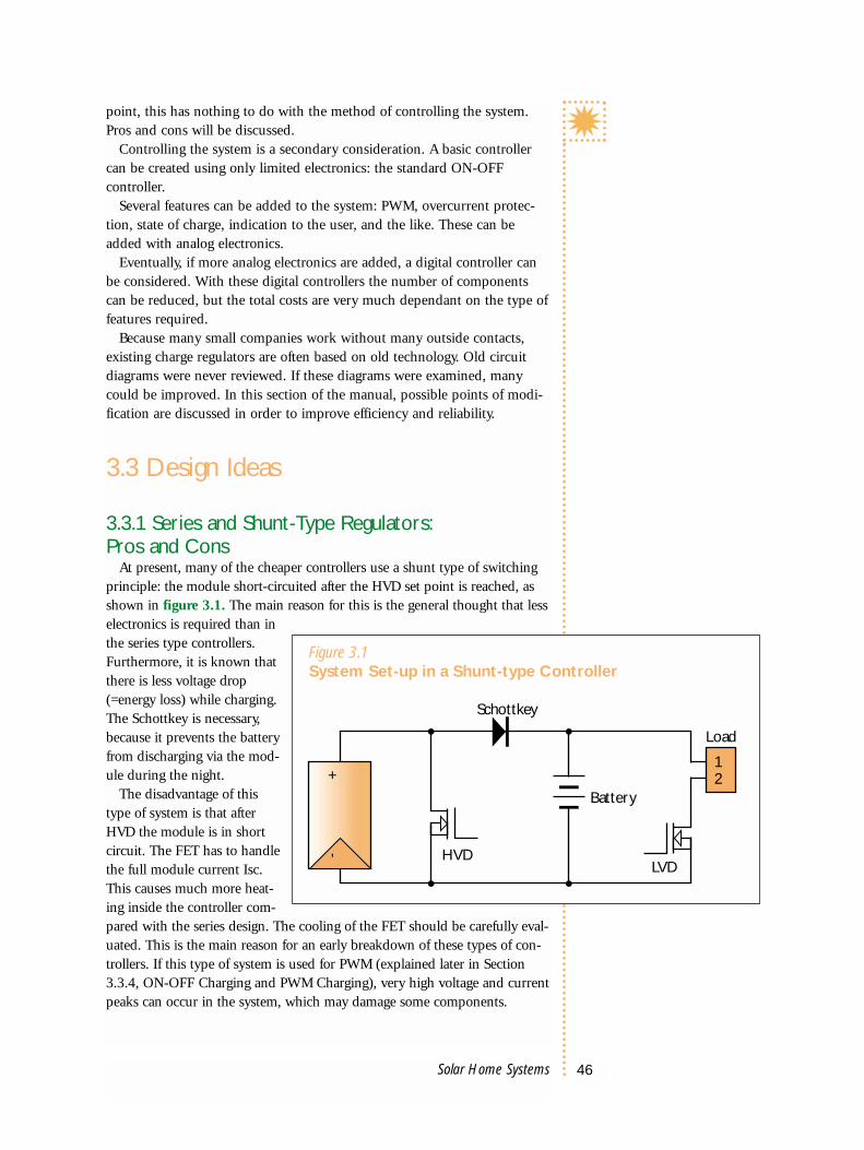
point, this has nothing to do with the method of controlling the system.Pros and cons will be discussed.
Controlling the system is a secondary consideration. A basic controllercan be created using only limited electronics: the standard ON-OFFcontroller.
Several features can be added to the system: PWM, overcurrent protec-tion, state of charge, indication to the user, and the like. These can beadded with analog electronics.
Eventually, if more analog electronics are added, a digital controller canbe considered. With these digital controllers the number of componentscan be reduced, but the total costs are very much dependant on the type offeatures required.
Because many small companies work without many outside contacts,existing charge regulators are often based on old technology. Old circuitdiagrams were never reviewed. If these diagrams were examined, manycould be improved. In this section of the manual, possible points of modi-fication are discussed in order to improve efficiency and reliability.
3.3 Design Ideas
3.3.1 Series and Shunt-Type Regulators:Pros and Cons
At present, many of the cheaper controllers use a shunt type of switchingprinciple: the module short-circuited after the HVD set point is reached, asshown in figure 3.1. The main reason for this is the general thought that lesselectronics is required than inthe series type controllers.Furthermore, it is known thatthere is less voltage drop(=energy loss) while charging.The Schottkey is necessary,because it prevents the batteryfrom discharging via the mod-ule during the night.
The disadvantage of thistype of system is that afterHVD the module is in shortcircuit. The FET has to handlethe full module current Isc.This causes much more heat-ing inside the controller com-pared with the series design. The cooling of the FET should be carefully eval-uated. This is the main reason for an early breakdown of these types of con-trollers. If this type of system is used for PWM (explained later in Section3.3.4, ON-OFF Charging and PWM Charging), very high voltage and currentpeaks can occur in the system, which may damage some components.
46Solar Home Systems
Figure 3.1System Set-up in a Shunt-type Controller
Load
Battery
Schottkey
HVD
+
' LVD
12

An additional problem is that the World Bank states that the controllermust have protection against reverse polarity connection for both the mod-ule and the battery. As can be seen in figure 3.1, this shunt design will defi-nitely have problems with this requirement. A power FET always containsan internal freewalk diode, in the opposite direction of the switched cur-rent. If the module is connected with reverse polarity, it will immediatelybe in short circuit via this freewalk diode. In itself this is not a major prob-lem, if the cooling is sufficient. But if the battery is connected with reversepolarity the FET and/or the Schottkey will burn immediately. There are twosolutions to avoid this problem and meet the World Bank standards: Add a fuse in the module line, just before or just after the Schottkey
diode; or Add an extra Schottkey diode just before or just after the HVD-FET (in
the FET shunt itself), in the direction of the module short circuit current.The second solution adds an extra critical component to the controller,
but the user or technician does not need to make repairs after making awrong connection. The extra energy loss in this Schottkey is of no impor-tance, because what is lost would be lost anyway. It is used when the mod-ule is disconnected. The first solution is the simplest one.
Some controllers however, are designed according to the series principle,as shown in figure 3.2.
Because of the internalfreewalk diode in T1, theSchottkey is still necessary.
The main disadvantage isthe extra energy loss in T1.You will therefore need tolook over the data sheetsvery carefully. The lower theinternal conducting resist-ance is, the lower the energyloss. This internal resistancediffers considerably for differ-ent types and different manu-facturers, and can varybetween 0.3 and 0.01.
Section 3.4.5, LightningSurge Induction, explains theeffects of lightning-induced transient pulses in both types of systems. TheHVD MOSFET is less stressed with a series design than with a shunt design.
Other advantages of a series configuration for solar home systemsinclude the following: The series FET has less voltage applied across it during all phases of
operation when compared to the shunt FET (Section 3.4.5, LightningSurge Induction).
Less switching noise in a series design. Greater precision in battery charging, while the charging current is
actively manageable. Pulse charging is possible.
47Solar Home Systems
Figure 3.2Basic Diagram of a Serial, Negative-Switching SHS Controller
Load
Battery
Schottkey
T1
+
' T2
12

3.3.2 Positive Switching and Negative SwitchingIt is known that there are significant problems in the field with solar
home systems. The customers and technicians sometimes do not knowwhat the cause is, and sometimes they even bypass the controller. This onlymakes the problem worse, but they know of no other solutions. One of thecauses is possibly unknowingly bypassing some controller functions. Inmost of the present controllers the 0V wires are switched. If the moduleand some load, or the controller itself, is connected to “ground,” the FETsare in short circuit via this ground. Even the connections seem correct.Furthermore, in electronics it is common for the black wire to be connectedto ground. For customers who work with electronics and do not know thesystem sufficiently, this can be very confusing and cause problems. Forexample, the module is connected to the roof. If this roof is made of metal,there is a chance the module is connected to earth (depending on the mod-ule construction). If the controller is now connected to ground, the HVDfunction does not work. The battery is overcharged every time. The dam-age can be so great that the battery becomes defective within 3 months.Nevertheless, the system set-up appears to be correct.
In a second example, almost all DC and AC converters have a groundconnection at the box. When this device is connected to ground somehowwith the charge regulator as well, the total LVD function is bypassed. Evenwhen the AC load is switched OFF, the quiescent current of the converteris flowing from the battery all night.
The only way to make sure that this will not happen is to switch the+–wires from all devices. Now everything can be connected to groundwithout problems. Additionally, if the solar systems are interfered with, nodamage is caused to the controller or the battery. Switching the positivelines contributes to the general reliability of the complete system.
The aim of the charge regulator design is to keep the electronics as sim-ple as possible.
When using the usual N-channel FETs for this positive switching, it willbe very difficult to drive this component. The drain should be connected tothe module, the source to the +battery. The gate voltage should be at least10V higher than the source voltage in order to activate it (Vgs = +10V).Just before HVD the battery voltage will be about 14.5V. The gate voltageshould be at least 24.5V. When the charging has to be stopped, Vgs mustbe 0V. This means that the gate voltage should be the same as the batteryvoltage. It will be difficult to create this precision steering.
Another solution is the use of P-channel FETs with Vgs = –10V, as shownin figure 3.3. In the positive switching system the source voltage is themodule voltage. If we make the gate voltage 0V (Vgs = –12V during charg-ing) the FET is conducting. If the gate voltage is 22V (Voc from the mod-ule) Vgs = 0V so it is blocking. In this type of FETs the drain-source cur-rent (Ids) is also negative, what is required. The steering principle for the“load-FET” can stay the same, only exactly opposite towards a negativeswitching system. For the set points, we use Schmitt triggers again. Anexample of the use of Schmitt triggers can be found in the total diagram inappendix 1. The reference voltage can be taken towards the ground. Onlythe module FET needs a voltage doubler, for a disconnected module terminal has
48Solar Home Systems

the open circuit voltage (Voc). For a proper blocking of the module current, thegate voltage should be at least Voc = 22V.
Another solution is to add a DC–DC converter to the module, so that the inputvoltage is fixed. Then the voltage doubler for the module FET is not needed.
Only when a currentlimiter is desired, thereference voltage shouldbe taken toward thepositive system voltage.More details on this canbe found in Section3.4.4, SafetyPrecautions: OverloadProtection and ShortCircuit Protection. Theonly difference is thatnow all reference volt-ages are trimmedtowards the +Voltage ofthe battery, as discussedin appendix 1. The ref-erence is taken from thepositive voltage insteadof the ground (Z3). Because of this, the Schmitt triggers have to function inthe opposite way.
The total costs for positive switching controllers will be a little higher,but the configuration is safer and more logical to the people in the field.
3.3.3 HVD Switching in the Battery Line:Pros and Cons
In serial disconnect controllers the module is totally disconnected fromthe system at HVD. In parallel controllers the module is brought in shortcircuit at HVD. The practical problem for the latter type of regulators isthat the cooling for the FETs has to be high. The cooling is insufficient inalmost every inexpensive parallel controller. This causes early breakdown,because the FET has to handle the full module short circuit current Isc.
A different approach is to place the module FET in the battery shunt. AFET always contains a reverse polarity freewalk diode that can handle thesame current as the FET itself, which is really convenient for this methodof use.
The line to the battery is now divided into two directions. One way isalways open via the diode. That is the direction for the load current. TheFET can block the opposite direction. That is the direction for the chargingcurrent. In the case of HVD the FET only blocks this charging current. Thebattery is still able to give energy to the load. The big difference is that themodule is also still connected to the load. The load can use the possibleenergy from the module after HVD. For example, the battery is fullycharged at 4 p.m. The module is totally disconnected in the standard typeof systems. If the user wants to listen to the radio at that time, the energy is
49Solar Home Systems
Figure 3.3Basic Diagram of a Positive-Switching Charge Regulator
LoadBattery
MOSFET P
MOSFET PT1+
'
T2
12

taken from the battery until the battery level is below the module reconnectvoltage. In the meantime the possible energy from the module is wastedinstead of used by that radio. If the FET is placed in the battery shunt, theload can directly use the energy from the module while the battery is still inHVD mode. This has a double benefit. The possible module energy is notwasted, and energy is not taken from the battery, but saved for later use.
There are some disadvantages to this system: Energy stored in the battery has to flow through an extra diode before it
gets to the user. (It has to run twice through the HVD–FET.). This meansa slight loss of energy. This principle is only worthwhile if it is certainthat the extra module energy retrieved after HVD will be used during theday. The system should be slightly overdimensioned, meaning the mod-ule should be a little too large for the battery, and energy should be usedduring daylight. Systems in hospitals and schools could be based on thisprinciple.
When the “Charging-FET” is blocked and charging current is stopped, thesystems’ voltage would increase to the open circuit voltage of the module.This could damage the connected user devices. At the moment that themodule is disconnected from the battery, a dump load should be connect-ed to the system. This load has to be sufficiently large that the modulevoltage (and so the system voltage) does not exceed the maximum of14.5V. According to our experience, solar home systems of 150Wp need tolose about 3 to 4A in order to reach that voltage. The more loads are con-nected, the less current needs to flow to the dump load. This is about thesame effect as a DC–DC converter on the module itself, but such a DC–DCconverter can also increase the module voltage when it is lower than a cer-tain output voltage. This device can also be used for this purpose.An important technical aspect of this system is that the electronics power
supply should be taken straight from the battery, “V+” shown in figure 3.4,because if you take the V+ from the total system (“C+”), problems willoccur with the set points.
Without current flow the set points can be correctly trimmed. As soon asload is connected, thereis a certain voltage dropover T1. This FET isnow in the batteryshunt. The system volt-age measured by thecontroller is not theactual battery voltage.This depends on thecurrent flowing throughT1. If the battery is dis-charged at a rate of 3Athe LVD set point willdrop to 10,1V. If charg-ing at a rate of 3A theHVD set point willincrease to 16,2V.
50Solar Home Systems
Figure 3.4Basic System for HVD-Switching in the Battery Line
Load
Battery
Shunt MOSFET PMOSFET P+
'
T2T1
V+
C+ C–
12
Steering
0 V
14.5 V

3.3.4 ON-OFF Charging and PWM ChargingA 1992 PV battery survey noted that most PV controllers use a simple
ON–OFF regulation mechanism (see figure 3.5). These controllers interruptcharging early in the cycle when a voltage regulation set point is reached. Toprevent instability, a hysteresis of 1 volt is generally used to reconnect the PVarray, and this causes the battery voltage to driftdown for a period of time before charging canstart again. A 1994 report by the U.S. researchinstitute, Sandia National Laboratories, foundthat batteries charged with the standard setpoints will typically average between 55 percentand 60 percent state of charge (SOC) for a peri-od of years. This causes stratification of the elec-trolyte and sulfation of the battery plates, thusincreasing internal resistance, which furtherreduces charge efficiency.
There is another algorithm to charge batteries:Pulse Width Modulation. During the last part ofthe charging cycle, where the ON–OFF regulationshould disconnect the module, the module isswitched ON and OFF with a certain frequency.Normally the voltage of the car battery goes downwhen the charging device is removed. By connect-ing and disconnecting the charging device with aduty cycle, charging can go on much longer andthe battery will reach a much higher state of charge. The duty cycle is the ratiobetween the ON time and the OFF time of the charging current.
The potential benefits of charging a PV battery with controlled pulsesinclude the following: Compact lead sulfate can be broken up to improve battery capacity and
charge acceptance. Charge efficiency can be improved and effects of aging can be reduced. Operating life of the battery can be increased. Higher voltage pulses can punch through resistive coatings between the
grid and active material on the plates. The opportunity for a gas bubbles to form can be reduced. Down pulses further improve charge efficiency and reduce gassing.
One especially exciting area of pulsing may offer particular benefits forPV systems. The PWM charge pulses may be short enough in duration toreduce the chance that gas bubbles will form. Further, it seems that a downpulse makes gassing even less likely since it apparently helps to break upthe precursor to a gas bubble.
With a PWM algorithm, there are constant voltage charging values forlead-acid batteries that provide for rapid charging and a safe regulation ofvoltage. These are between 2.35 v/cell and 2.40 v/cell where the batteryenters the gassing stage. For effective PV charging, the proper constantvoltage must be held within a narrow window.
Figure 3.6 shows the charge characteristic from a battery while it isbeing charged with a constant maximum current (from point 0 until 4hours). When each cell reaches its maximum voltage of about 2.30V, the
51Solar Home Systems
Figure 3.5Low-Cost ON-OFF Charge Regulator

battery is being charged with a constant voltage. When the battery reachesits (almost) full state of charge, its accepted charging current will decreaseto 0.2xImax. This is the point at which maintenance charging starts (after 8hours) and from then on the cells will be more overcharged.
These three stages ofcharging are called tricklecharging. While normalON–OFF regulators stopthe whole charging processwhen the cell voltage is atits maximum, as shown infigure 3.6, trickle chargingcontinues for four hoursuntil the battery reaches itsfull state of charge (100percent). When the cellvoltage just reaches it max-imum value, the actualstate of charge is only 60percent. Hence with stan-dard ON–OFF regulatorsthe battery is never fullycharged.
Figure 3.6 applies charg-ing without PWM, but withdrip loading in order tocompensate for the self-discharge of the battery (maintenance charging). Thisdoes not take place in PWM charge regulators, because these controllers keepcharging until the duty cycle is zero. If there is self-discharge of the battery, alow duty cycle will again be initiated.
A standard ON–OFF controller will stop charging at the HVD point.Without regulation the voltage will increase further. Due to this high voltage,gassing will occur, and this can be dangerous under normal operating condi-tions. The voltage should be kept at 14.5V, the “constant voltage algorithm.”
In order to charge the battery with maximum power, the average charg-ing current should be decreased in such a way that the system voltage staysat 14.5V. This can be done with pulse-width modulation (PWM). The dutycycle has to be decreased so that the average charging current pulls the(open circuit) battery voltage up to 14.5V. While going to its “fullycharged” state, the (virtual) open circuit voltage will rise steadily to 14.5V.The difference of the HVD voltage and this open circuit voltage will steerthe duty cycle (D.C.):
D.C. (%) = A x (HVD – Vbat (open))This system should be triggered only at the moment that the battery,
charged with DC = 100%, approaches the HVD set point.From another point of view, when the charging voltage approaches
14.5V, the duty cycle has to be reduced. Figure 3.7 shows a possible blockdiagram for this type of PWM.
52Solar Home Systems
12 2.7
2.5
2.3
2.1
1.9
1.7
1.5
10
8
6
4
2
00 2 4 6 8 10
Time (h)
Supplementaryovercharge
Overcharge,caused by V-charge
I-charge U-charge 1a
Current
Voltage[A
]
[V]
Figure 3.6Charging Current Acceptance from a Lead Acid Battery
Note: The voltage and current are shown on the vertical axis.

Morningstar’s “Prostar” was one of the first digital controllers to use this algo-rithm. The SunSaver 6 (see figure 3.8) is Prostar’s analog brother. Both controllersare known as very efficient charge controllers, which extend the lifetime of the bat-tery to the maximum. Unfortunately,less attention is paid to the safety pre-cautions. See sections 3.4.2, SafetyPrecautions: Reverse PolarityProtection, and 3.4.3, Reduction of theNumber of Components.
The PWM controllers tested byECN had basic frequencies rangingfrom 8Hz to 300Hz. The basic fre-quency should not be too high (nothigher than 10kHz for prevention ofthe battery skin effect, discussed inChapter 2), and constant over thecharging range. Batterycharging is a chemicalprocess, and it needs sometime to start up before it iseffective. If the chargingcurrent is switched off toosoon, the actual energy stor-age has not yet started. TheMorningstar Sunsaver uses300Hz. The Sunsaver algo-rithm turned out to be oneof the most effective chargeregulators, but it is not clearif it will be even more effec-tive if the basic frequency isbrought down farther.
The result for TheMorningstar Sunsaver 6 isshown in figure 3.9.
As can be seen, whenthe current is cut off, adown pulse is generatedthat can approach –10A.Morningstar has investigated the effect of this down pulse, and states thatthis characteristic has a beneficial impact on the lifetime of the battery.
In a PV system, a down pulse (that is, reverse or discharge pulse) willoccur when charging in PWM with a load. Research indicates that there aregood prospects for using pulse charging combined with down pulses toextend battery life in PV systems. The following benefits may be possible: The down pulse creates new activation sites, so with subsequent pulses,
there are more sites available to accept charge. Pulses break through corrosion to prevent capacity loss. Sulfation is reduced. Heating and gassing of the battery during charging is reduced.
53Solar Home Systems
Figure 3.8Morningstar's SunSaver Charge Regulator
20 kHz
PWM outVBat.
Vref.
A
Figure 3.7Block Diagram for Constant Voltage PWM Algorithm

3.3.5 Boost ChargingAll batteries require some overcharging now and then to reverse sulfation
and reach full charge. The finishing charge is of critical importance toenable recharging to 100 percent SOC while avoiding excessive heatingand gassing.
Gassing in the battery, which is initiated by some small overcharge,cleans the internal plates. If this is done once every three weeks, it willreduce battery deterioration and increase deep recharge capacity.
The normal HVD set point should be as follows: 14.1V (2.35V/cell) for sealed batteries at 25ºC. 14.4V (2.40V/cell) for flooded batteries at 25ºC.
While boost charging these HVD set points are temporarily increased toabout 14.5V and 14.8V at 25ºC.
Some solar home system controllers incorporate the function of this“Boost Charging.” The biggest difference between the various types of con-trollers is the timing when the boost charging takes place. Some controllers only boost charge the battery when it is connected for
54Solar Home Systems
InputC1
PeriodRisetimeFalltime
Freq.+Width–Width
Vp–pPreshootOvershoot
s/Div1.00 ms
Delay1.0000 ms
Displayoptions
Sampleperiod
Data acquired at 2.00 msNext acquisition: 2.00 ms
Figure 3.9SunSaver-6 PWM Results: Voltage against Time for Three Different Duty Cycles
+
+
+

the first time, just after installation. This costs more in electronic circuits,while the boost function is not very effective.
Others will apply the boost charge function every time the LVD set pointis reached. In this way, the extra sulfation is removed shortly after it isformed on the plates. However, overcharging too frequently also is notrecommended, because this will shorten the battery lifetime. The result ofthis type of boost timing is that the deterioration of the battery will accel-erate with age. Charging and discharging of a battery will be faster withthe age of the battery. The older the battery, the more often it will reach itsLVD and HVD points. The boost charging voltage will be applied to thesystem more frequently. In the end it is only boost charging.
The optimum situation seems to be to make boost charge possible aboutonce every three weeks.The purpose of boost charging is generally accepted, but is difficult to
achieve with only a few analog components. Therefore, boost charging afterevery time the system falls below its LVD set point seems a practical alter-native. It can be achieved with relatively few extra components.
The next section explains more about microprocessor-controlled chargeregulators. Since the total control of the system is provided by software inthese types of controllers the “ideal boost” is easy to add as extra compo-nents are required.
This function of boost charging is essential in areas where the tempera-ture is subject to large fluctuations. This boost charging is recommendedespecially in tropical countries and desert areas. However, there are doubtswhether this high voltage is often achieved. In practice people use as muchas possible, so probably the average state of charge will be relatively lowand HVD often will not be reached. In addition to this the module qualityis important. As previously described, in the Indian desert the temperatureeffect on the (locally manufactured) module is such that it cannot generate14.5V in the first place. So the HVD point is never reached. In these casesa question can be asked about the usefulness of the boost charge function.However, in ideal systems it is essential in certain geographical areas.
3.3.6 Special Function ICsAs solar energy becomes increasingly accessible for commercial use,
more and more special regulator ICs are being developed. Various manu-facturers design special function circuits to include many types of differentfeatures. Only a minimum of external components needs to be added inorder to create a fully functioning charge regulator. The main set-up ofsuch a charge regulator is illustrated in figures 3.10 and 3.11.
The disadvantage of these chips is that its features are fixed. It is not pos-sible to add extra features or change characteristics. In most special func-tion ICs for this purpose, a low-voltage disconnect for the load is notincluded, so external load control is necessary. Many professional manufac-turers therefore prefer a custom design rather than a standard solution thatis also available for private technicians.
Other special function ICs have a PWM algorithm integrated. Theswitching FET should be added externally.
55Solar Home Systems

Table 3.1 describes some of the special function ICs available for chargeregulators for lead-acid batteries.
3.3.7 Digital or Analog Set-upMost charge regulators are designed with analog electronics. This is par-
tially an inheritance from the slow development of charge regulators in thepast. In recent years much has changed to improve microprocessor tech-nology. One-chip processorswith internal A/D conversion,EEPROM, PWM generator,and the like have becomeavailable in all price classes.This reduces the number ofsystem components to a min-imum. Only a few analoginputs and steering outputsare then required in the regu-lating part of the circuit.
The great advantage of aprocessor-controlled regulatoris that extra functions (orchanges in actual functions)can be edited very easily. Ascan be seen in figure 3.12,the hardware for the temper-ature compensation and forthe state of charge indicationis reduced to a minimum.
A standard processor (with-out extra functions, such asADC and PWM) costs about$2.50 for large productionquantities. Since there is noADC on board, this shouldbe created externally. ThisADC can be made in variousways, so attention has to bepaid to the ADC design andthe total price.
Processors with specialfunctions cost considerablymore—about $10. Thismakes external ADC worthwhile in a digital design. If such a charge regula-tor is being developed, the engineer should be aware of and consider otheroptions. For every extra option on a microprocessor, the price rises dispro-portionately. In the near future, single-chip microprocessors will becomecheaper and more advanced.
Sometimes it is worthwhile to base the design on analog electronics. Thisdepends on which functions are required by the manufacturer. For the
56Solar Home Systems
Shunt
Transistor
Current regulator
LEDs
U
I
DCSolar panel
Functions:• Start charging• Current trimming• Module disconnect• Guarding
Figure 3.10ON-OFF Charge Regulator Based on Integrated Circuit
+–
U
I
Transistor
Solar panelDC
Figure 3.11PWM Charge Regulator Based on Integrated Circuit
Shunt
LEDs
PWM
Functions:• Start charging• Current trimming• Module disconnect• Guarding
+–

design of a standard ON–OFF controller, analog electronics is relativelymuch cheaper and effective. Even a PWM function as described in Section3.3.4, ON–OFF Charging and PWM Charging, can be realized with analogcomponents and still compete in price with a digital version.
Since the improvement of charge regulators is a recent development,there will be a growing interest in processor-based charge regulators.Microprocessors have a high calculation capability. This can be used todetermine the state of charge with complicated algorithms. Research isbeing performed on the use of ampere-hour balances for calculating theexact state of charge of the battery.
3.4 Modification Points
3.4.1 Quiescent Current ReductionIn small PV systems, energy saving is a major issue. This is true not only
for the user, but also for the designer of the system. All unnecessary energyloss is a waste. “Efficiency” is a keyword in the balance of system (BOS)components. Therefore, charge regulator designs should be continuouslyrevised with a view to decreasing its quiescent current. Every mA reductioncan be spent by the user, and makes the system more efficient.
In a simple calculation, if the system has a life expectancy of 15 years, itmeans that 1 mA quiescent current reduction adds the following to thetotal energy used: 0.001A x 12V x 15year x 365days x 24hour = 1577watt-hour. Every 5 mA quiescent current reduction results in about 1per-cent more energy available to the user.
The majority of the quiescent current of a basic analog ON–OFF chargeregulator goes to the following parts:
57Solar Home Systems
Table 3.1.Special Function ICs for Charge Regulators
DisconnectType Manufacturer algorithm Special
MAX 1648 Maxim Analog programmableUC3909 Unitrode None PWM
Temperature compensationBQ2031 Benchmarq U,2V,I,t PWM
Temperature compensationICS1735 Galaxy Power None Pulse charge and conditioningMTA11200 Microchip -U, dT/dt External current steering
uP-basedSOC monitoring
LT1510 Linear Tech. None: external switch PWM at 200kHzneeded internal end-amp
BST9303 Becker System LED status displayBST9705 BST Softcool algorithm LCD capacity display

Reference voltage. Power supply for the main electronics. Superfluous components. Voltage dividers.
A discussion of specific elements of some of these parts follows.Reference voltage. Comparing the battery voltage with a certain reference
voltage normally creates set point control. Different components can be
58Solar Home Systems
Schottkeyblockingdiode
Loaddisconnect-reconnectcircuit
Buzzer
PWMcurrentshuntcircuit
PowerFET
+ PANEL(max 21 V)
–
+5 V regulator
78L05+5 V out
Clockcrystal
Charge equalizationInterrupt
Reset
Temperaturesensingcircuit
+5 VLINE
LM335Z
Temperaturesensor
Resistance
Batteryvoltagesensingcircuit
Battery
PA0-PA3, PB0-PB7input/output channels
LOAD
LED indicators
BAT + (max14.5 V)
Relay
Low-voltage warning
1VDD VSS
20
2TIMER PAO
3OSCIN
19
OSCOUT4
5 NM1
8 TEST
7 RESET
8PB7
9PB6
10PB5
PA1 18
PA2 17
PA3 16
PB0 15
PB1 14
PB2 13PB3 12
PB4 11
Figure 3.12Example of a Microprocessor-Based Charge Regulator

used to create this reference voltage. In most diagrams, as in figure 3.13,you can find a Zener diode.
There is a disadvantage tousing a Zener diode in thisway. Its quiescent current isalmost always more than itneeds to be. The voltage dropover R1 at a battery voltage of14.5V will be 6.5V. With areference current of, forexample, 0.03 mA, its valuemust be 22k for optimumefficiency. At a battery voltageof 11.5V this should be 12K.Which resistor should youchoose? If you chose 22k andthe battery voltage is 11.5V,the reference is “too weak”and its voltage will drop. Ifyou take 12k and the batteryvoltage is 14.5V, a lot of ener-gy loss will take place in R1and Z1 in order to maintainthe 8V reference. In the endthe resistor ends up inbetween these two values.
A better solution is a refer-ence IC (figure 3.14). Do notuse the standard 78X seriesfor analog references, because these are made for power supplies. Theirquiescent current is too great for this purpose. The ICs TL431 or REF25Zare more suitable, because they are designed to maintain the reference volt-age at a fixed level with minimum energy loss over the input voltage range.This IC can be a simple substitute for the Zener diode.
This reference voltage will now be about 2.50V, so the other resistorsneed to be recalculated. However, the quiescent current is significantlydecreased.
Power supply for the main electronics: If digital electronics is used in thecontroller, a +5V power supply is needed, which means selecting the78X05 power supply. There is, however, a good substitute for this IC: theLP2905. This is also a 5V power supply, but has less quiescent current. Ingeneral, try to avoid digital flip-flops or CMOS ports in an analog-basedcontroller. Do not use them, unless it is absolutely necessary. Of course, inmicroprocessor-based controllers, a 5V power supply is a must.
Voltage dividers: All electronics make use of voltage dividers, for example,for measuring the battery voltage and trimming the reference voltages onthe opamp. If the charge regulator is dimensioned properly, try to doubleall resistor values, or at least some voltage dividers.
59Solar Home Systems
P1Z1 = 8 V Output
R1
11.5 –14.5 V
Input
Figure 3.13Reference Voltage with Zener Diode
Figure 3.14IC Replaces Zener Diode
7K87
TL431
P1 OutputInput

3.4.2 Safety Precautions: Reverse Polarity Protection Most stand-alone SHS are being used in remote areas, far away from a
service center. This requires all BOS components to be very reliable. If acomponent becomes defective, it will take a great deal of effort, time andmoney to replace it. Users should also have a reason to be confident in therelatively expensive solar system. In the “ideal” solar system no BOS com-ponents can be damaged by any mistake, not even an accidental wrongconnection. The main issue is to design the controller in such a way that itcan withstand all conceivable mistreatment.
This safety starts with the system itself. If all cables to and from the con-troller are equipped with plugs that can connect in only one way, the possi-bility of reverse polarity is already excluded. Of course both installationtechnicians in the field and users sometimes try to “repair” their systemthemselves if it does not meet their requirements. That is why a controllerfor remote areas should be able to withstand all types of wrong connections.
The World Bank has drafted a number of requirements regarding polarityprotection for both the battery and the module.
The electronics itself has to be protected. If a 78X power supply is used(with digital controllers), the downstream electronics is protected, but sen-sitive components before the IC are not. The safest way is to use a simplediode such as 1N4148 from the systems’ voltage to the electronics. In suchway the electronics are unharmed.
Protection of the system against improper polarization:This implies that the module and battery as well as the user should not
be endangered by a wrong connection. If the module is wrongly connected,no current should be able to flow, otherwise sparks may occur while dis-connecting. Figure 3.1 and figure 3.2 show the series and the shunt con-troller. The Schottkey diode in the shunt controller prevents the batteryfrom discharging during the night. If the modules’ polarization is opposite,it is in full short circuit via the internal safety diode. The Schottkey cannotbe placed before the FET (from the module point of view) because then atHVD the battery is brought into short circuit. If the battery is connectedwrongly, it will be in short circuit via the two diodes. As previously stated,an extra diode or a fuse should be added into this system.
In the series controller the Schottkey and the safety diode are directedexactly opposite. This system is safe for wrong polarization of both themodule and the battery. No current will flow, so it is safe for both the sys-tem and the user.
If the module is switched in the battery line, as shown in figure 3.4, andthe battery is connected with reverse polarity, the electronics is not pow-ered up. The module FET will not be activated, and the safety diode isblocking. Whenever the module is connected wrongly, the Schottkey isblocking. The system is now safe.
3.4.3 Reduction of the Number of ComponentsWith the foregoing in mind, we turn to appendix 2 and analyze the
upper picture of the charge controller. It has a quiescent current of 25mA.Four comparators monitor each one set point (HVD, HVR, LVD, and LVR).Every comparator has its own reference voltage. In pairs they steer a digital
60Solar Home Systems

flip-flop, which steer the FETs directly. This means that the steering voltageis only 5V. When this voltage is compared with the FET graphics shown inappendix 3, “transfer characteristics,” it shows that there is only about 17AIds (pulsed) possible. At Vgs = 10V the FET allows 110 A Ids pulsed. Thismeans that the internal resistance at Vgs = 5V as well as the energy loss inthe FET are much higher than necessary.
Under the “actual diagram” a possible alternative set-up is pictured. Byusing the opamps in a different way, most of the original electronicsbecomes redundant. The FET gs-voltage can now be 12V, so less heat isproduced inside the controller because of the lower internal resistance. Thequiescent current is now 5mA, which can be further reduced by replacingthe Zener diode with the reference IC, as shown in appendix 4.
Some controllers use more components than needed for their properfunction. Always look for a chance to combine functions. All references canbe led down from one voltage reference.
3.4.4 Safety Precautions: Overload Protection and Short Circuit Protection
For the standard analog ON–OFF controllers concerned, the cheapestway is switching with two opamps in “Schmitt trigger” form. When using a14-pin opamp housing such as LM324, two opamps are used. With someinexpensive components added, an electronic fuse can be created to maxi-mize the benefits of the available electronics. Appendix 5 shows a possibledesign of such an overload protection for a negative switching system. Thecurrent limit is adjustable from 0 to 10 amperes. If that limit is exceeded,the load will be shut down for one minute. That gives the electronics timeto cool down, and the user some time to switch off some of the load. Afterthis interval of one minute the load is automatically switched on again.This method of overload protection is much more user friendly than a fuse.In remote areas it is sometimes difficult to buy fuses. With this type of pro-tection, replacement of fuses is no longer necessary. How does the electron-ics work?
Measure the load current. If it is more than 80 percent of the maximumFET current Ids (this is a generally accepted standard; components shouldbe capable of handling 125 percent of the maximum system ratings) or acertain other current value, the load should be disconnected. The electron-ic fuse in a negative switching system gives a good indication on how itfunctions. Then combine the E-fuse with a positive switching system. Theprinciple remains the same, but the electronics functions exactly in theopposite way.
In the negative switching systemAppendix 5 shows the diagram of the current limiter in the negative
switching system. A shunt resistor is added to measure the load-current.The voltage across this resistor is compared with a reference (IC1d).Normally the output from pin 14 as well as from pin 8 is 0V. C4 is dis-charged via T3 / R16, because T1 is conducting. If the load-current exceedsthe limit, the output from pin 14 is 12V. Pin 8 is still at 0V, so pin 10 willbe about 4V. The IC1c output from pin 14 will flip to 12V. Now T1, as well
61Solar Home Systems

as the load, is shut off via T4. No load current is flowing, so the outputfrom pin 14 will return to 0V. Pin 10 will have 8V. The output from pin 8also slowly charges the capacitor C4. It takes about a minute to reach 8V.This is the point when the output from pin 8 turns to 0V again. T1becomes active, C4 is being discharged, and the system is back in its origi-nal state. If there is still an overcurrent, this principle repeats itself.However, the time interval will only be the discharge time of the capacitorC4, which is a fraction of a second. C3 and R15 must be added, in order tosuppress ON–OFF switching peaks. Otherwise the current limiter willrespond every time a lamp is switched ON. When the controller is con-nected for the first time, then the input from pin 12 responds slower thanthe reference pin 13 due to C3. Therefore the current limiter stays off afterthe first installation. The system is now balanced correctly.
In the positive switching systemThe normal positive switching controller works in exactly the same way,
but referenced from the systems +–voltage. Appendix 6 shows the samediagram, but now for the positive switching regulator.
As indicated earlier, the electronics power supply should be takenstraight from the battery. This is in order to keep the set points stable. Thereference voltage for the Schmitt triggers will have to come from the +–bat.Appendix 6 shows a prototype diagram with the current limiter. IC1d isthe overcurrent detector, IC1c is a one-minute timer. As soon as FET T1 isconducting again, the timing capacitor C4 has to be discharged. So thisdischarging is depending on the opposite state of the T1 output. If T1 ishigh, there should be no discharging, if T1 is low C4 has to be discharged.That is why we need two transistors here. In the negative-switching regula-tor we also used two transistors, so there are no components added.
3.4.5 Lightning Surge InductionMost standards in the world state that lightning surge induction protec-
tion inside the charge regulator is needed. This is an essential point,because in some areas lightning occurs very frequently. Temporary over-voltages can have many causes, but in solar home systems, the mostimportant one is lightning induction in the cable from the module.
Because there is less system-level protection, small PV systems are moresensitive for voltage transients than larger PV systems, where the price ofthe electronics is of less importance.
The Morningstar Corporation formed a project to study the effects oftransient induction on small solar systems. They also investigated two typesof protection devices: the metal-oxide varistor (MOV) and the transientvoltage suppressor (TVS). Most small charge regulators use MOVs, becauseTVSs are much more expensive. Both devices work by shorting the tran-sient current, so they are connected in parallel with the module input.
Figure 3.15 shows a standard IEC pulse definition used in order to sim-ulate the transients representative of field condition. Figure 3.15 shows thatthe resulting peak in voltage, caused by the transient current pulse, is high-er with a MOV than with a TVS. These TVSs are mainly used in moreexpensive systems.
62Solar Home Systems

Transients have many causes other than lightning, and it is very difficultto design for a 15-year operating life when considering how much expo-sure a PV controller will have to transient pulses.
63Solar Home Systems
µsec
(a) AT&T Standard (b) IEC801-5 Level 1
Volts
Volts
00
10
20
30
40
50
60
70
80
90
100
µsec
0
10
20
30
40
50
60
70
80
90
100
1,000 2,000 3,000 4,000 5,000 6,000 0 100 120 140 160 18020 40 60 80 200
Figure 3.15The IEC Standard Test Pulse for Testing the Transient Overvoltage Protection
MOVMOV
TVS TVS
Pulse (amps) Pulse (amps)
Amps: Rise Fall Peak Repetitions10 µsec 1,000 µsec 10 amps 3,000
Device: DC MaxPart standoff clamping
Size number voltage voltageTVS 1,500 W Z 6039 31.6 V 51MOV 15 mm Z 15L390 31.0 V 77
Amps: Rise Fall Peak Repetitions8 µsec 20 µsec 43 amps 5
Device: DC MaxPart standoff clamping
Size number voltage voltageTVS 1,500 W Z 6039 31.6 V 61MOV 15 mm Z 15L390 31.0 V 95
Time Pulse TVS MOV µsec amps volts volts
0 0.00 0 02 2.00 40 604 4.00 43 666 6.00 46 728 8.00 49 74
10 10.00 51 77200 8.50 50 76600 6.50 48 73
1,000 5.00 45 682,000 2.50 41 623,000 1.20 40 584,000 0.60 39 575000 0.30 39 565,900 0.10 39 556000 0.00 0 0
Time Pulse TVS MOV µsec amps volts volts 0 0.00 0 0 2 10.00 46 77 4 21.00 52 80 6 32.00 57 86 8 43.00 61 95 12 34.00 59 87 16 27.00 57 82 20 22.00 53 80 40 11.00 47 78 60 5.50 43 70 80 2.50 40 63100 1.20 39 60120 0.60 39 57140 0.30 39 54160 0.15 39 52180 0.07 39 50200 0.00 0 0

In a reliable analysis of an 8/20 pulse (the IEC801–5 level 1 standard fortransient pulse testing) the varistor (MOV) would clamp the FET to 60V.However, in a series design the resulting voltage across the FET would beonly 47.6V, as shown in figure 3.16.
As can be seen in figure 3.16, the seriesFET is between 60V transient and the 12Vbattery. This produces only 47.6V, whichis well within the (normally) 60V rating.
The shunt design, however, places theFET directly between the positive leg andthe ground. This produces the full 60Vacross the FET. In addition, the Schottkeybecomes a second component to bestressed by the transient. This means thatthe series design offers a greater degree ofprotection.
During a transient pulse, the systemvoltage stays at 12V, and the workingpoint of the module drops back to zero inits power curve, which means that themodule itself and the cables absorb theenergy of the transient pulse. This cannever fully be the case because theresponse time of the Schottkey diodealways is almost as long as the 8/20 pulse.While the Schottkey is not fully open, thesituation shown in figure 3.16 will be thecase. As soon as the diode is conducting, aslight dip in the working point of themodule may occur, but it will not droptotally to zero. By that time the transientpulse is already over.
3.4.6 Oscillation Problemswithout Battery
A solar home system is designed for charging batteries. The battery is the“buffer” for the systems’ voltage. A module without any load gives an opencircuit voltage of 21V. When the battery is disconnected, the system voltagewill immediately go to its HVD action, and shut off the module. The elec-tronics does not have any power left to keep the FET conducting, becausethere is no battery connected. When the module is in open circuit again,the voltage rises to 21V. This repeats itself. The LEDs blink on the frontpanel. The speed of this oscillation depends on the total capacity of thecontroller. In itself this sequence is harmless. However, it can cause damagein shunt regulators.
In shunt controllers, the module is brought into short circuit at HVD.This means that there is always a maximum current flowing at HVD.Because of the oscillation, the average gs-voltage is about 5V. This meansthat the internal resistance of the FET is higher, and it has to handle the
64Solar Home Systems
Figure 3.16Transient Voltage Drops in Solar Home Systems
Battery
+
'
T1
60 V
60 V12 V
48 V
Battery
60 V
(b) Series regulator
(a) Shunt regulator
47.6 V
12 V
0.4 V
T1+
'

full module current. This causes more heat than in a series regulator, whereno current flows during oscillation.
The oscillation problem is relevant for all tested controllers and bothcontroller types. This is typical for a working controller: disconnect themodule at HVD. In shunt controllers, this can cause overheating.
“Oscillating” is perhaps not the right word. It is more a “logical ON–OFFswitching” which is normal for any controller. It is recommended that theoscillation speed not be too high, for example 0.5Hz. This can be achievedby adding a 100(F/50V capacitor straight over the power supply of thecomparators. In this way the blinking disconnect-LEDs indicate that thereis no battery connected. For shunt-type regulators, the biggest problem isthe cooling of the FET. The stronger hardware has sufficient cooling. Asmall piece of metal surface is not enough. In cheaper types of charge regu-lators this is the main reason for failure.
A more expensive solution is a “battery detection circuit.” If there is nobattery connected, this circuit changes the Module-FET into a “dummy-load” and disables a module disconnect. The comparator LM324 can han-dle Vcc = 30V max, so that is no problem. This may be an ideal solution,but is costly in terms of extra components.
Better solutions are possible, but our overall guidance is clear: “We needto keep the design as inexpensive as possible.”
65Solar Home Systems

66Solar Home Systems

Chapter 4DC–AC Conversion
4.1 Scope of Work
The use of DC–AC inverters in small solar home systems is growingrapidly. In some areas it is unthinkable to sell an SHS without one.Hence it is a worthwhile exercise to consider the advantages and
disadvantages of using these devices, and to determine the purposes forwhich they can be used.
First, the most common applications of DC–AC conversion can be listed: Televisions. Many people in rural areas have built up savings to buy a
color television, sometimes with a satellite dish. Lighting. In some rural areas standard 230Vac fluorescent lamps are used
instead of the special 12Vdc fluorescent lamps because they are easy toobtain.
Fans. In tropical areas a fan is often desired. This is a luxury item, whichusually is bought only after a television set is obtained. This device con-sumes a lot of energy, so it can be incorporated only in larger systems.
Refrigerators. The demand for refrigerators is growing, especially in areaswhere people have already worked with solar energy for some time.These devices also consume a lot of energy, so the dimensioning of thesystem has to be kept in mind.In many smaller devices (satellite receivers, radios, and the like) 230Vac
input is transformed to 12Vdc. In televisions this dc voltage is transformedafterwards to the high kVoltage to drive the electron beam to the screen.The use of a DC–AC converter for these devices is theoretically rather use-less. DC–AC converters have an efficiency of approximately 85 percent.Downwards AC–DC transformation always has energy losses also, in theorder of 90 percent efficiency. In total it means an unnecessary energy lossof 100% – (90% x 85%) = 23%.
At present there are many types of television sets, satellite receivers and flu-orescent lamps operating at 12Vdc. Solar energy is relatively expensive, sodevices that are used in combination with an SHS should be selected carefully.
On the other hand there are some important, these 12Vdc devices can-not yet be sold with an SHS in rural areas for very practical reasons: Televisions: 12Vdc television sets are sometimes far too expensive, com-
pared to the 230Vac versions. The market for 12Vdc televisions, outsidethe solar home system market, is very limited and mainly based onWestern prices. It will take quite some time before the price for this typeof device and its availability can compete with the 230Vac television.
Lighting: The lack of fluorescent lamps in some areas is a problem.Traveling nomads in northern China prefer a DC–AC converter with a230Vac fluorescent lamp because 230Vac FL are available in almost every
67Solar Home Systems
Large parts of this sectionof the manual notes weretaken from the followingpublications: PowerElectronic Converters: DC–ACConversion, Guy SéguierFrancis Labrique, SpringerVerlag (Berlin andHeidelberg), 1993. PowerElectronics: Converters,Applications and Design.Ned Mohan,Tore M.Undeland,William P.Robbins, John Wiley &Sons, 1995. 200Watt PowerInverter by ELV GmbH,1993. A DC–AC IsolatedBattery Inverter usingHIP4082, application noteIntersil, May 1996.

village they encounter. From the aspect of energy consumption, this isnot a good solution. In areas where 12Vdc FLI can be delivered, howev-er, it must be recommended to use these, because it is an important fac-tor in getting the most out of a solar system.
Refrigerators: At present, research is being performed in the field of12Vdc refrigerators. It will still take some time for efficient units to enterthe market at a reasonable price. Present 12Vdc designs use far too muchenergy for a small SHS. A 230Vac refrigerator with DC–AC converter ismainly used, but only in combination with larger PV systems.It is important to note that DC–AC converters in combination with very
small systems (up to 50 or 100 Wp) are not of much use (though some-times practical). 230Vac equipment in general uses more energy than nec-essary. When the energy loss in the DC–AC converter is added to thisunnecessary energy loss, there is not much left for other applications.
Taking this into consideration we can derive suitable basic structures fora DC–AC converter that can be used in solar home systems. This is veryimportant, because there are many different ways to design them. Manydifferent topologies are described in the literature. Much information isavailable about power electronics and DC–AC conversion for a wide seriesof applications, unlike information about charge regulators and FLIs for12Vdc. On the other hand, the technology of DC–AC converters is muchmore complicated than the technology of the otherBOS components.
In this project we focus on solar home systems,so the examples we have chosen in this chapter areespecially suitable for that purpose. Normally, thepower limitation for DC–AC converters in SHS isset on 500 watt maximum (see figure 4.1). Set-upswithin this power range are different from set-upsdesigned for 5,000 watts, for example. The basicpower topology may be the same, but safety regula-tions and technical specifications are different. Forexample, it is hard to find a full sine wave inverterunder 500 watts for a price that is suitable for cus-tomers in developing countries.
The common DC–AC converters sold within theSHS market must not only be as cheap as possiblebut also very reliable. In this chapter we will focuson topologies, set-ups, and examples that can befound within this scope.
4.2 Types of Inverter: PrinciplesWe present the principle of the various inverter types for a single-phase
output, by using the four- “switch” (K1, K2, K'1, and K'2) configurationshown in figure 4.2. The supply placed on the DC side is assumed to beperfect, as are the switches (zero forward voltage drop, zero leakage cur-rent, instantaneous commutation).
i and u are used to denote the input current and voltage,
68Solar Home Systems
Figure 4.1250–500 Watt DC-AC Inverter from LUE

i' and u', the output current and voltage,iK1, and vK1, the current and voltage across K1,T, the operating cycle of the inverter and its output values.The inverter is assumed to be in “full-wave” control I, that is– for 0 < t < T/2, K1 and K'2 are on and K2 and K'1 off.u' = u i = i'
iK1, = i', vK1 = 0– for T/2 < t < T, K2 and K'1 are on, K1 and K'2 are off:u' = –u, i = –i'
iK1 = 0, vK1 = u.If the variations in iK1 and vK1 are followed, the currents in the
other switches and the voltages across them can be directly deduced:iK'2= iK1, vK'2 = vK1,iK2 = iK'1 with iK'1 (t + T/2) = iK1 (t)vK2 = vK'1 with vK'1(t + T/2) = vK1(t)
Voltage-source invertersA voltage-source inverter is an inverter fed by a DC voltage supply,
that is, by a supply with negligible internal impedance; its voltage uis not affected by the variations in current i flowing through it. TheDC supply imposes the volt-age at the input—and thusat the output—of theinverter.
If u is constant andequal to U, whatever thevalue of i,
for 0 < t < T/2, u' = + Ufor T/2 < t < T, u' = – U.The output current i'
and thus the input currenti depend on the loadplaced on the AC side.This load can be of anytype, provided that it isnot another voltage source(capacitor or AC EMF) connected directly across the output terminals.
Switch K, must be made up of a fully controlled (turn-on and turn-off)switch TC1. It must connect terminal 0 to terminal M at instant t = 0 andseparate these two terminals at instant t = T/2, whatever the AC load maybe. For iK1 to flow via K1, if the latter is momentarily negative, an antiparal-lel connected diode D1 has to he added to TC1.
The basic diagram of the autonomous voltage inverter can thus be pro-posed, as in figure 4.3.
To show the influence of the load on the operation required of the semicon-ductor devices, we will consider the load to be perfect, that is, that it takes a sinu-soidal current. The cases of the inductive and capacitance loads are considered.
Figure 4.4 provides the waveforms of u', i', i, vK1, and iK1 when the load isinductive (current i' lags voltage u' fundamental component).
69Solar Home Systems
M
K
K
K
K
N
Figure 4.2Basic Diagram of a Full Bridge
TC1D1
K1
K'1
K2
K'1K2'
K'2
K1' K'2
D2
D'1 D'2TC'1
TC2
TC'2
i
i'
u'
u'
u
U
U
U
0
2TT
t
t
U
iK1
iK'1
iK2
iK'2
Figure 4.3Basic Diagram of an Autonomous Voltage Inverter

For switch K1,from t = 0 to t = t1, diode D1 enables i', which is then negative, to flow;from t = t1 to t = T/2, TC1 enables i' to flow;at instant t = T/2, turning off TC1 leads to i' being transferred from TC1
to D'1.
Three remarks can bemade about this opera-tional mode: For t = t 1, TC1
begins conductingwhen the current iszero; no overcurrentis produced in thisdevice and no over-voltage across it.
Controlled devicesTC1 and TC2 turn-ondrive signals must beapplied throughoutperiod [0, T/2] (andthat of TC2 and TC'
1
throughout period[T/2, T]), since thevalue of t1 dependson the load.Although TC1 is con-trolled at turn-onfrom t = 0, it remainsnonconducting until t= t1, when it starts toconduct.
A short period of timemust be left betweenthe turn-on of TC'
1 (orTC'
2) and the turn-offof TC1 (or TC2) andvice versa, in order toavoid short-circuitingthe DC voltage supply.On account of the diodes, there is no risk of the AC current load circuitbeing opened.Figure 4.5 shows the waveforms of u', i', i, vK1, and iK1 when the inverter
feeds a capacitativeload (current i' leads voltage u' fundamental component).At instant t = 0, firing TC1 means that current i' is transferred from diode
D'1 to TC1; i' flows via the latter until t = t1.For t = t1, current i' falls to zero and becomes negative, TC1 turns off nat-
urally and D1 becomes conducting. D1 conducts until instant t = T/2 whenit turns off as a result of the turn-on of TC'
1.
70Solar Home Systems
i'0
i'0
i'0
i'0
t1
t1
t1
t1
t1
D2 D2
D1 D'1TC'1TC2
TC1
TC'2
i'
i
u'
+
+
U
U
U
t
t
t
t
t
0
0
0
0
0
0
T
T
T
T
T
iK1
iK1
vK1
vK1
2T
2T
2T
2T
2T
2T
2T
Figure 4.5Capacitative Load Waveforms
turn-on
i'0
i'0
i'0
i'0
t1
t1
t1
t1
t1
D2 D2
D1 D1 TC'1TC2
TC1
TC'2
i'
i
u'
+
+
U
U
U
t
t
t
t
t
0
0
0
0
0
0
T
T
T
T
T
iK1
iK1
vK1
vK1
2T
2T
2T
2T
2T
2T
2T
Figure 4.4Inductive Load Waveforms
turn-off

As in the case of a flow across an inductive load, there is one commuta-tion with neither overcurrent nor overvoltage. The other commutation isensured by the turn-on of a controlled device. The ability for turn-off is notused in this case.
If the load can be either inductive or capacitative, the semiconductorswitches must be controllable at both turn-on and turn-off.
4.3 DCVoltage SupplyImperfection Input Filter
In the case of inverters,the effects giving themost problems arise fromthe inductance in the pathwhere the current must besuddenly reversed: DC supply inductance
in a voltage-sourceinverter.
AC load inductance ina current-sourceinverter.
Voltage spikesIn order to take into
account the non-zerovalue of inductance Ls ofan imperfect voltage sup-ply u, this supply isreplaced by a perfectvoltage source Us seriallyconnected with thisinductance Ls, as infigure 4.6.
u = Us – Ls di/dt. When feeding an induc-
tive load, during eachcommutation, current imust go from |i'o| to –|i'o|, as shown in figure4.3; this rapid decreasein i leads to a voltagepeak u.Figure 4.6b indicates
the waveforms
71Solar Home Systems
VD1
VT1
VT'1
VT'1
VD'1
iD'1
iT'1
iD'1
iT'1
Us
UsUs
Us
Us
t
u
i
t
t t
uu
i
i
tt
∆u
∆u
(b) (c)
0 0
0 0
0 0
iD1
iT1iD1
LS
TC1
D1
TC'1
D 1
D2
D'2
TC2
TC'2
US
iT1
VT1
–Us–Us
VD1
VD'1
i'
–i'oi'o
i'o
i'o
–i'o
–i'o
–i'o
i'o
(a)
Figure 4.6Waveforms

of vD1, and iD1 (or of vD'2 and iD'2)of vT'1 and iT'1 (or of vT2 and iT2),of i, equal to iT'1 – iD1, since iT'1 equals iT2
of u, equal to Us – Ls di/dt.during the TC'
1 - D1 (or TC2 - D'2) commutation, which occurs when, for
t = 0, the turn-off of TC'1 (and TC2) is controlled.
Since vT1, equals u + vD1, the peak voltage u appears in the voltageacross TC’1; moreover, it can be increased by the forward voltage peak ofdiode D1. When feeding a capacitative load, during each commutation, current i goes
from – |i'o| to |i'o|, as shown in figure 4.4; this leads to a voltage through u.During the D'
1 –TC1 commutation controlled by the turn-on of TC1. Thereverse current peak in diode D'
1 can be found in the waveform of iT1 and,multiplied by 2, in that of i; it causes a voltage peak.
The input filterIn order to “correct” the DC voltage supply, a capacitor C
is connected in parallel across the inverter input, as shownin figure 4.7. This eliminates the sharp variations in u dur-ing commutations and reduces this voltage ripple during theperiod between commutations.
Capacitor C, together with inductor Ls—whose value canbe increased by adding an external inductance to the DCsupply—form a low-pass filter: for voltages, in the supply to inverter direction, for currents, in the inverter to supply direction.
This enables a voltage u which is practically constant tobe obtained at the inverter input, despite variations in i andeven if voltage US is affected by a ripple (for example, in thecase of voltage supplied by a rectifier). It also enables cur-rent i, taken from the supply to be kept practically constant,while current i at the inverter input shows an important ripple. The cost ofthe filter decreases as the inverter operating frequency increases.
Battery supplyA battery is a current-reversible DC voltage supply. It is thus particularly
well adapted to supplying a voltage-source inverter and can ensure the func-tional reversibility of the latter. For operation in the inverter mode, themean value of i is positive and the battery discharges. During recovery, themean value of i is negative and the battery charges up. A capacitor with avery low inductance is usually connected in parallel across the battery asthe latter opposes very fast variations in the current.
An input filter can be used—see figure 4.6—to reduce the current ripplesupplied or received by the battery.
Choosing the inverterFor those inverters, intended to supply an AC load normally of highly
variable impedance from a battery or a rectifier, a voltage-source invertershould be chosen. Such a choice is made for the following reasons:
72Solar Home Systems
iS LS
US
Cu
Inverter+
Load
i
Figure 4.7Correcting the DC Voltage Supply

The battery is particularly well adapted to supplying a voltage-sourceinverter. If necessary, an L-C filter can reduce the ripple of the currentdelivered by the battery. Such a filter enables a rectifier to supply a volt-age-source inverter.
The operation of a voltage-source inverter is highly affected by theimperfections in the DC supply and hardly at all by those of the AC load.The reverse applies to the current-source inverter. For the uses beingconsidered here, the DC supply can be selected but not the AC load.
Neither of the inverters directly gives a sinusoidal output voltage and anoutput filter must be used. In the case of the voltage-source inverter, thevoltage to be filtered is imposed by the DC supply and the exact wave-form to be filtered is known. With the current-source inverter, the volt-age to be filtered depends on the load.
4.4 Single-Phase Inverters TopologiesIf only two “switches” are used obtain an AC voltage from a DC voltage,
a midpoint is necessary on either the AC output or DC input side.This corresponds to the following:
The single-phase inverter with center-tapped primary output transformer(often called a push-pull inverter).
The single-phase inverter with a capacitative divider at the input (often calleda half-bridge inverter).If the relative width of the square-wave pulses forming the output volt-
age half-cycles has to be varied, four “switches” are necessary. This is thesingle-phase bridge (or fullbridge) inverter.
4.4.1 Single-PhaseInverter withCenter-TappedTransformer
Figure 4.8 provides theconfiguration for the nota-tions used for the single-phase voltage-source inverterwith two “switches” and acenter-tapped primary trans-former. The DC voltage sup-ply has a terminal connectedto the midpoint 0. Its otherterminal is connected eitherto A by the conduction ofTC1 or D1, or to B by theconduction of TC'
1 or D'1.
73Solar Home Systems
i´
u´
n2
A
B
U
K1
K1
D1
TC1
TC1
n1/ 2
n1/ 20
v1
v1*
*
*
iK1
iK1
D1
i+–
VK1
VK1
Figure 4.8Notations for a Single-Phase Voltage-Source Inverter withTwo Switches and a Center-Tapped Primary Transformer

PrincipleIf the transformer is assumed to be perfect, for example, if the resistances
and leakage inductance of its windings are ignored, the voltages are in rela-tion to the number of turns:
v1 = v'1, u' = v1 2n2 /n1
If the magnetizing m.m.f. is ignored, the primary and secondary currentsare linked by the compensation in m.m.f.:
n1 /2 (iK1, –iK'1) = n2 i'.
Commutations required In the case of an inductive load, the commutations are forced. For t =
T/2, when TC1 is on, its conduction must be interrupted. This results ina voltage equal to + 2U across it; the current (2n2/n1)i' is transferred fromTC1 to D1.
In the case of a capacitativeload, the commutations are natural. For t = 0,when D'
1 is on, TC1 is fired. This results in a voltage equal to –2U acrossdiode D'
1, which turns off. Current (2n2/n1)i' is transferred from D'1 to
TC1. In both cases, during each half-cycle, there is a free natural commutation
between the semiconductor devices of a same switch—from D1 to TC1 orvice versa, or from D'
1 to TC'1 or vice versa. This occurs when i' reverts
its polarity.
Doubling the voltageThe presence of a center-tapped transformer means that the reverse volt-
age across the diodes and the forward voltage across the controlled devicesare equal to twice the DC supply voltage:
–vDmax = vTmax = 2U.
4.4.2 Single-Phase Half-Bridge InverterThe single-phase half-bridge inverter uses two “switches” which are bidi-
rectional in current and a center-tapped voltage supply. The midpoint canusually be obtained by usingtwo capacitors C1 and C'
1
with the same capacitance C.If the latter is sufficient, twovoltages that are virtuallyconstant and equal to U/2 areobtained. Figure 4.9 showsthe configuration and thenotations used.
PrincipleAs the sum of the voltages
uC1, + uc'1 across the twocapacitors is equal to U andas this voltage is assumed tobe constant,
uC1 + uC1' = U
74Solar Home Systems
i
U
C1
C1
ic1
ic1 i
u
UC 1
UC 1TC1
TC1 D1
D1
K1
K1
VK 1
VK 1
iK 1
iK 1
Figure 4.9Single-Phase Half-Bridge Configuration

givesC duC1/dt, = –C duC1'/dtiC1 = –iC1'
The charging (or discharging) current of C1 is equal to the discharging(or charging) current of C'
1.sincei' = iC'1 – iC1,i' = 2 iC'1 = –2 iC1
Current i', which reaches the midpoint of the capacitativedivider hastwice the value of the current in one of the capacitors.
Commutations requiredThe commutations required are the same as those for the push-pull
inverter: Forced commutations TC'
1 –D1 and TC1 –D'1 when supplying an induc-
tive load Natural commutations D'
1 –TC1 and D1 –TC'1 when supplying a capaci-
tative load.
Doubling the currentOwing to the capacitative divider, the current in the ON switch is twice
the current in the DC supply.IK1 or iK'1 = 2i
4.4.3 Single-Phase Full-Bridge InverterThis is the full-bridge structure that was used in the previous chapter to
present the various inverters. The configuration of the voltage-sourceinverter is shown again in figure 4.10.
In the previous chapter, it was assumed that switches K, and K'2 were onduring the first half-cycle of voltage u’, making the latter equal to + U; switch-es K2 and K'1 were on during the other half-cycle, making u’ equal to –U.
This control mode uses only a part of the possibilities of the full-bridgevoltage-source inverter,because the latter enables notonly the voltage frequencybut also its value to be varied.
PrincipleThe control signals of K1
and K'1 must be complemen-
tary in order to avoid short-circuiting the voltage U sup-ply and opening the current i'
circuit. Similarly, for theother half-bridge, the con-trols of K2 and K'
2 must becomplementary. However thecontrols of both half-bridgesneed not be simultaneous;there may be a phase-shiftbetween the two.
75Solar Home Systems
U
i
VK1VK2
VK 1VK 2D 1
K 1
i´
K 2
D2
TC 2TC 1
iK 1iK 2
u´
iK1iK2
TC2TC1 D1
K1 K2
D2
Figure 4.10Full-Bridge Structure

If is once again used to denote the angular frequency of the fundamen-tal component voltage u', angle can be used to characterize the phaseshift between the control signals:
K1 is on for 0 < t < ; K'2 for < t < +
K'1 is on for < t < 2; K2 for + < t < 2 + .
Commutations requiredThe types of commutation required no longer depend solely on the
nature of the AC load (positive or negative ) but also on angle .Switch K1 lets current i flow from t = 0 to t = ; this current reverses
its polarity during this period. If i' is negative for t = 0, D1 conducts firstof all and TC1 then begins conducting when i' becomes positive; for t = ,TC1 must turn off current I' and perform a forced commutation.
If i' is positive for t = 0, TC1 takes the current which then goes via D1
and is naturally transferred to TC'1 when the latter is turned on at instant
t = /.
4.5 Galvanic IsolationOften galvanic isolation is required between the high-voltage AC output
and the DC input voltage. This can be achieved by either a low-frequencytransformer at the output side of the inverter or by a high-frequency trans-former inserted before the inverting output bridge.
The main advantage of a high-frequency transformer is its reduced sizeand hence cost and weight compared to the rather bulky and heavy 50Hztransformers. However, the creation of a high-frequency waveform andsubsequent rectification requires additional circuitry and increases thecomplexity of the inverter. However the DC voltage often needs to bestepped up before the final inverting at the output bridge. In this case thehigh-frequency transformer can provide both isolation and voltage boost. Alow frequency transformer at the output of the inverter has the additionalbenefit of serving as a filter for disturbances at the load side that effectivelyprotects the semiconductor devices from the output bridge.
In the following section some issues are discussed regarding thedesign and construction of high-frequency transformers for switchedpower supplies.
Isolation transformer representationA high-frequency transformer is required to provide electrical isolation.
Neglecting the losses in the transformer of figure 4.11b, an approximateequivalent circuit for a two-winding transformer is redrawn in figure 4.11c,where N1:N2 is the transformer winding turns ratio, Lm is the magnetizinginductance referred to the primary side, and Lt1 and Lt2 are the leakage induc-tances. In the ideal transformer, v1/v2 = N1/N2 and N1i1 = N2i2.
In a switch-mode converter, it is desirable to minimize the leakageinductances L t1 and L t2 by providing a tight magnetic coupling betweenthe two windings. The energy associated with the leakage inductances hasto be absorbed by the switching elements and their snubber circuits, thusclearly indicating a need to minimize the leakage inductances. Similarly, in
76Solar Home Systems

a switch-mode DC-DC con-verter, it is desirable to makethe magnetizing inductanceLm in figure 4.11c as high aspossible to minimize themagnetizing current i, whichflows through the switchesand thus increases their cur-rent ratings.
Power transformers that aresmall in weight and size andhave low power losses are themost desirable. The motiva-tion for using high switchingfrequencies is to reduce thesize of the power transformerand the filter components. Ifthis benefit is to be realized,the power loss in the trans-former core should remainlow even at high frequencies.
Ferrite materials such as3C8 are commonly used tobuild transformer cores. As infigure 4.10a, figure 4.12ashows a typical B-H loopfor such a material,where the maximum fluxdensity Bm beyondwhich the saturationoccurs is in a range of0.2–0.4 Wb/m2 and theremnant flux density Br
is in a range of 0.1–0.2Wb/m2. In figure 4.12b,the core loss per unitweight for severalswitching frequencies isplotted as a function ofBmax) , where (Bmax) isthe peak swing in theflux density around itsaverage value duringeach cycle of the switch-ing frequency fs.
In the full-bridge con-verter with a bidirection-al core excitation, asshown in figure 4.13:
77Solar Home Systems
III
IBm
Bt
B
H
(a)
(b) (c)
AN1
N2
B CD
A C
D
Lt1
i1
N1:N2
Lm v1 v2
Lt2Ideal
B
+ +i2
Figure 4.11Transformer Representations: (a) Typical B-H LoopTransformer Core, (b) Two-Winding Transformer,(c) Equivalent Circuit
Hysteresis curve
Core lossvs. flux density
H (Oersteds)(a)
Courtesy of Ferroxcube Division of Ampereex Electronics Corp.
–0.5 00
1,000
2,000
3,000
4,000
5,000
0.5 1.0 1.5 2.0 2.5
100oC
25oC
3 96 1512 22
10-6
10-5
10-4
10-3
10-2
10-1
1.0
101
102
103
48248248248248248248248248248
8
10 102 1031Flux density (Gauss)
(b)
4 2 84 2 284
200 kHz
1 kHz2 kHz
3 kHz5 kHz
100 kHz
50 kHz20 kHz
B (G
auss
)
Figure 4.123C8 Ferrite Characteristics Curve: (a) B-H Loop,(b) Core Losses Curves

(Bmax) < Bm.Based on the previous discussion, the following conclusions can be
reached regarding the desiredcore properties: A large value of maximum
flux density Bm allows(Bmax) to be large andresults in a smaller coresize.
At switching frequenciesbelow 100 kHz, for exam-ple, (Bmax) is limited byBm. Therefore, a higherswitching frequency resultsin a smaller core area.However, at switching fre-quencies above 100 kHz, asmaller value of (Bmax) ischosen to limit the corelosses.
In a converter topologywhere the core is excited inonly one direction, (Bmax)is limited by Bm–Br.Therefore, it is important touse a core with a low rem-nant flux density Br in sucha topology unless a com-plex-core resetting mecha-nism is used. In practice, asmall air gap is introducedin the core that linearizesthe core characteristic andsignificantly lowers Br.In the converters with bidirectional core excitation topologies, the pres-
ence of an air gap prevents core saturation under start-up and transientconditions. But this does not prevent core saturation if there is a volt-sec-ond imbalance during the two half-cycles of operation (a volt-secondimbalance implies that a dc voltage component is applied to the trans-former core). In a practical implementation, there are several causes ofsuch a volt-second imbalance, such as unequal conduction voltage dropsand unequal switching times of the switches. The preferable way to avoidcore saturation due to these practical limitations is to monitor switch cur-rents, as is done in the current. Use of an appropriate control integratedcircuit (IC) also eliminates saturation under start-up and transient condi-tions. The other way to prevent core saturation due to voltage imbalance isto use a blocking capacitor in series with the primary winding of the half-bridge and the full-bridge inverters. The blocking capacitor should he cho-sen appropriately so that it is not too large as to be ineffective under tran-
78Solar Home Systems
t
t
iD1 iD1
iL
ton ∆
io
(b)
(a)
0
0
Vd VoN2N1
Ts2
( )
D1
N2N1
N2
vL
v1
iL
iD1
D2
T3T1
Vd
T2T4
+
–
+
–
+–
+
–
+ – io
voi
Figure 4.13High-Frequency Transformer with Bidirectional CoreExcitation (Using Full-Bridge Topology)
Voi

sient conditions and not too small to cause a large ac voltage drop across itunder steady-state operating condition. In the push-pull converters, thecurrent-mode control is used to prevent the switch currents from becomingunequal.
4.6 Comparison of the RequiredComponents and Characteristics
The two types of two-switch voltage-source inverters (push-pull andhalf-bridge) require only two controlled semiconductor devices and twodiodes, whereas the full-bridge inverter requires four controlled devicesand four diodes. This advantage of the two former inverters is, however,reduced by the doubling of the voltage or the current: For a given voltage U of the DC supply,
for the push-pull inverter, vTmax = –vDmax = 2 U,for the other two, vTmax = –vDmax = U.
For a given current i of the DC supply, the current in switch K1, when itis on, has the valueiK1 = |i| for the push-pull inverter,iK1 = 2 |i| for the half-bridge inverter,iK1 = |i| (or li'|) for the full-bridge inverter.The two-switch inverters require half as many semiconductor devices but
the voltage or current rating of the latter is doubled.The push-pull inverter requires a transformer and the half-bridge invert-
er requires a capacitativedivider, whereas the full-bridge inverter requiresneither. These disadvantages of the two-switch inverters are less importantthat it would initially appear.
Virtually all inverters require a transformer to ensure galvanic isolationand to obtain the desired output voltage amplitude. In the case of thepush-pull inverter, the transformer is inherent in the operating principle.However, the fact that it has a center-tapped primary and that each half-primary is only used during one half-cycle means that the primary powerrating is multiplied by square root (2).
Virtually all inverters require an input filter comprising an inductor anda capacitor. The capacitors of the half-bridge inverter also can act as a filter-capacitor. Instead of one capacitor of capacitance C submitted to voltage U,two capacitors (each with a capacitance 2C and submitted to a voltage U/2)are used.
The main difference is that the full-bridge inverter (more expensiveoverall) enables the output voltage to be varied and thus, to be regulatedmore precisely. The full-bridge inverter requires the conduction of twoseries-connected switches; the corresponding voltage drop and losses leadto a highly reduced efficiency when the voltage supply U has a relativelylow value.
Single-phase inverters with an output voltage consisting of only onesquare-wave pulse per half-cycle are used for low-power equipment, whichneeds to deliver a relatively stable AC voltage. A low-pass filter must beconnected between the inverter output itself and the AC load.
79Solar Home Systems

When there is low level of power, use two-switch configurations wherev-er possible: Use the push-pull inverter when the DC supply voltage has a very low
value (for example, for a 6 or 12 V battery); doubling the voltage is not aproblem in this case.
Use the half-bridge inverter when U is about 100 V (for example, ACvoltage mains seen via a transformer and a rectifier); doubling the cur-rent raises relatively few problems and producing the capacitative divideris not too costly.Only when the variations in input voltage U are important or when the
output voltage must be correctly stabilized by the inverter itself does thefull-bridge converter need to be used. In such cases, the mean operatingpoint is placed at equal to (š3. For this value, the harmonic ratio of volt-age u' is reduced and, most importantly, there is no third harmonic. Thismakes it easier to produce the output filter and increase the efficiency ofthe latter.
4.7 Square-Wave versus PWM Switching
4.7.1 Square-Wave Switching PrincipleIn the square-wave switching scheme, each switch of
an inverter leg of a full-bridge inverter is ON for onehalf-cycle (180º) of the desired output frequency. Thisresults in an output voltage waveform as shown in figure4.14a. From Fourier analysis, the peak values of the fun-damental-frequency and harmonic components in theinverter output waveform can be obtained for a giveninput Vd as
(VA0)1= 4/š VDC/2dand(VA0)h= (VA0)1/hwhere the harmonic order h takes on only odd values,
as shown in figure 4.14b.One of the advantages of the square-wave operation is
that each inverter switch changes its state only twice percycle, which is important at very high power levels wherethe solid-state switches generally have slower turn-on andturn-off speeds. One of the serious disadvantages ofsquare-wave switching is that the inverter is not capable ofregulating the output voltage magnitude. Therefore, the dc-input voltage Vdc to the inverter must be adjusted in orderto control the magnitude of the inverter output voltage.
4.7.2 PWM Switching SchemeIncreasing use is now made of pulse-width modulation
(PWM) to obtain a rough estimate of a sinusoidal voltageby forming each of the output voltage half-cycles of asuccession of suitable sized square-wave pulses. The
80Solar Home Systems
vAo
0
00.20.40.60.81.01.21.4
1
x
xx
x x x x x3 5 7 9 11 13 15
(a)
(b)
t
1( )f1
Vd2
Vd2
(vAo)1/Vd2
^
Figure 4.14Square-Wave Switching
( )
h(harmonicsof f1)

advantage of the full-bridge inverter, which enables the output voltagevalue to be varied, disappears since the other types can now also guaranteethis variation.
However, the two-switch inverters provide only two voltage levels (u' = +U or –U), whereas the full-bridge inverter gives three voltage levels(u' = +U or –U or zero).
The full-bridge inverter obviously makes it easier to approximate therequired sinusoid. This allows a more effective use of components and aneasier filtering. As soon as the power being used is important and theimportance attached toperformance (especially inreducing the overallweight of the equipment)becomes paramount, thefull-bridge inverter will beused.
In order to produce asinusoidal output voltagewaveform at a desired fre-quency in inverter circuits,a sinusoidal control signalat the desired frequency iscompared with a triangularwaveform, as shown in fig-ure 4.15a. The frequencyof the triangular waveformestablishes the inverterswitching frequency and isgenerally kept constantalong with its amplitudeVtri.
The triangular waveformvtri in figure 4.14a is at aswitching frequency fs,which establishes the fre-quency with which theinverter switches areswitched (fs is also calledthe carrier frequency). Thecontrol signal vcontrol isused to modulate theswitch duty ratio and has afrequency f1, which is thedesired fundamental fre-quency of the invertervoltage output (f1 is alsocalled the modulating fre-quency). It also recognizesthat the inverter output
81Solar Home Systems
x
x
x
x
xx
xx x
x xx
xx x x x x x0.0
1 mf
Harmonics h of f1
(mf + 2)
ma = 0.8, mf = 15
2mf 3mf
0.20.40.60.81.01.2
(vAo)hVd2
^
( )
(2mf + 1) (3mf + 2)
0
0
t
t
t = 0
Vd2
Vd2
vcontrol
vcontrol < vtri
vtri
vAo vAo , fundamental = (vAo)1
1( )fs (a)
(b)
(c)
TA – : on, TA + : off vcontrol > vtriTA + : on, TA – : off
Figure 4.15Pulse-Width Modulation
voltage will not be a perfect sine wave and will contain voltage componentsat harmonic frequencies of f1. The amplitude modulation ratio ma, is de-fined as
ma = Vcontrol/Vtri
where Vcontrol is the peak amplitude of the control signal. The amplitudeVtri of the triangular signal is generally kept constant. The frequency modu-lation ratio mf is defined as
mf = fs/f1
Since the two switches are never off simultaneously, the output voltagevAo fluctuates between two values (1¼2Vd and –1¼2Vd). Voltage vAo and itsfundamental frequency component (dashed curve) shown in figure 4.3b,which are drawn for mf = 15 and ma = 0.8.
The harmonic spectrum of vAo is shown in figure 4.15c, where the normal-ized harmonic voltages (VA0)/
1¼2Vd having significant amplitudes are plotted.This plot (for ma < 1.0) shows three important features of importance
1. The peak amplitude of the fundamental-frequency component (VA0)1
is ma times 1¼2Vd.2. The harmonics in the inverter output voltage waveform appear as
sidebands, centered around the switching frequency and its multiples, thatis, around harmonics mf, 2mf, 3mf, and so on. This general pattern holdstrue for all values of ma in the range 0–1.
3. The harmonic mf should be an odd integer. Choosing mf as an oddinteger causes only odd harmonics to be present, and the even harmonicsdisappear from the waveform of vAo.
4.8 Semiconductor Switches and Driver Circuits
4.8.1 Semiconductor Switches
Which types of switch can be used in each case?In voltage-source inverters (VSIs), the controlled semiconductor devices
must have diodes connected across in antiparallel; they do not have towithstand reverse voltage. If the load is always inductive, transistors with “long” control signals are
used for low and medium power equipment; operation as a dual thyris-tor is particularly well adapted to this operational mode. Care must betaken to supply the gate until the moment when the forward currentbuilds up.
If the load is always capacitative, classical thyristors are suitable, sincethere is natural commutation operation. Asymmetrical thyristors can beused.
Controlled turn-on and turn-off devices must be used in cases where theload can be of any nature. Power transistors for low- and medium-powerapplications can be used.
82Solar Home Systems

Metal-Oxide Semiconductor Field-Effect Transistors (MOSFETs)The circuit symbol of an n-channel MOSFET is shown in figure 4.16a. It
is a voltage-controlled device, as is indicated by the i-v characteristicsshown in figure 4.16b. The device is fully ON and approximates a closedswitch when the gate-source voltage is below the threshold value, VGs(u,).The idealized characteris-tics of the device operatingas a switch are shown infigure 4.16c.
MOSFETs require thecontinuous application of agate-source voltage ofappropriate magnitude inorder to be in the ONstate. No gate current flowsexcept during the transi-tions from ON to OFF orvice versa when the gatecapacitance is beingcharged or discharged. Theswitching times are veryshort, being in the range ofa few tens of nanosecondsto a few hundred nanosec-onds depending on thedevice type.
The on-state resistancerDS(on) between the drainand source of the MOSFETincreases rapidly with thedevice-blocking voltagerating. Because of this,only devices with smallvoltage ratings with lowon-state resistance andhence small conductionlosses are available.However, because of their fast switching speed, the switching losses can besmall. From a total power loss standpoint, 300-400-Y MOSFETs competewith bipolar transistors only if the switching frequency is in excess of30–100 kHz. However, no definite statement can he made about thecrossover frequency because it depends on the operating voltages, with lowvoltages favoring the MOSFET.
MOSFETs are available in voltage ratings in excess of 1,000V but withsmall current ratings and with up to 100 A at small voltage ratings. Themaximum gate-source voltage is (20V, although MOSFETs are available thatcan be controlled by 5V signals. Because their on-state resistance has a pos-itive temperature coefficient, MOSFETs are easily paralleled. This causesthe device conducting the higher current to heat up and thus forces it toshare its current equally with the other MOSFETs in parallel.
83Solar Home Systems
On
Off
0
iD
vDS
(c)
vDS
iD
0
On
Off
(b)
vGS = 7 V
6 V
5 V
4 V
vDS
S
DiD
+
–
(a)
vGS
–
+
G
Figure 4.16MOSFET Characteristics

Insulated Gate Bipolar TransistorsThe circuit symbol for an insulated gate bipolar transistor (IGBT) is shown
in figure 4.17a and its i-v characteristics are shown in figure 4.17b. TheIGBTs have some of the advantages of the MOS-FET, the BJT, and the GTO combined. Similar tothe MOSFET, the IGBT has a high impedance gate,which requires only a small amount of energy toswitch the device. Like the BJT, the IGBT has asmall on-state voltage even in devices with largeblocking voltage ratings (for example, Von is 2–3 Vin a 1,000V device). Similar to the GTO, IGBTscan be designed to block negative voltages, as theiridealized switch characteristics shown in figure4.17c indicate.
Insulated gate bipolar transistors have turn-onand turn-off times of the order of 1 µs and areavailable in module ratings as large as 1,700 Vand 1,200 A. Voltage ratings of up to 2–3 kV areprojected.
4.8.2 Gate and Base Drive Circuits
Preliminary design considerationsThe primary function of a drive circuit is to
switch a power semiconductor device from theOFF state to the ON state and vice versa. In mostsituations the designer seeks a low cost drive cir-cuit that minimizes the turn-on and turn-off timesso that the power device spends little time in tra-versing the active region where the instantaneouspower dissipation is large. In the ON state thedrive circuit must provide adequate drive power(for example, base current to a BJT or gate-sourcevoltage to a MOSFET) to keep the power switchin the on state where the conduction losses arelow. Very often the drive circuit must providereverse bias to the power switch control terminalsto minimize turn-off times and to ensure that thedevice remains in the OFF state and is not trig-gered on by stray transient signals generated bythe switching of other power devices.
The signal processing and control circuits thatgenerate the logic-level control signals used toturn the power switch ON and OFF are not con-sidered part of the drive circuit. The drive circuitis the interface between the control circuit andthe power switch. The drive circuit amplifies thecontrol signals to levels required to drive the power switch and provideselectrical isolation when required between the power switch and the logic-
84Solar Home Systems
On
Off
0
iD
vDS
(c)
vDS
iD
0
(b)
vDS
S
DiD
+
–
(a)
vGS
–
+G
E
C
G
vGS
Figure 4.17IGBT Characteristics

level signal processing control circuits. Often the drive circuit has signifi-cant power capabilities compared to the logic-level control signal process-ing circuits. For example, power BJTs have low values of beta, typically5–10, so that the base current supplied by the drive circuit is often a signif-icant fraction of the total load current.
The basic topology of the drive circuit is dictated by three functionalconsiderations. First, is the output signal, provided by the drive circuit,unipolar or bipolar? Unipolar signals lead to simpler drive circuits, butbipolar signals are needed for rapid turn-on and turn-off of the powerswitch. Secondly, can the drive signals be directly coupled to the powerswitch, or is electrical isolation required between the logic-level control cir-cuits and the power device? Most electrically isolated drive circuits willrequire isolated de power supplies. Thirdly, is the output of the drive cir-cuit connected in parallel with the power switch (the usual situation) or inseries with the switch (cascode connection)?
Additional functionality may be required of the drive circuit, which willfurther influence the topological details of the circuit. Provisions may beincluded in the drive circuit design for protection of the power switch fromovercurrents. Then communication between the drive circuit and the con-trol circuit is needed. In bridge circuits, the drive circuit must often pro-vide blanking times for the power switch. Incorporation of these types offunctionality requires design inputs to both the drive circuit and the logic-level control circuit. Wave shaping of the drive circuit output might also beincluded to improve the power switch performance.
The specific details of component values to be used in a drive circuit willvary depending on the characteristics of the power switch being driven.For example, MOSFET drive circuits need only provide an initial large cur-rent as the device turns ON and for the rest of the on-state time intervalmerely provide a large gate-source voltage at low current levels.
It is a good idea to consider how the drive circuit will be configured on acircuit board even at the earliest stages in the design process. The placementof components to minimize stray induc-tance and to minimize susceptibility toswitching noise may affect the choice oftopology for the drive circuit.
DC-coupled drive circuitsA simple MOSFET gate drive circuit with
only one switch to control the gate currentis shown in figure 4.18, where the outputtransistor of a comparator (for example,LM311) controls the MOSFET. When theoutput transistor is OFF, the MOSFET isON and vice versa. When the comparatoris on, it must sink a current VGG/IR1, and toavoid large losses in the drive circuit, RIshould be large. This will slow down theMOSFET turn-on time. This means that thedrive circuit is only suitable for low switch-ing speed applications.
85Solar Home Systems
+
–
Fromcontrolcircuit
VGG
RR2
Figure 4.18Simple MOSFET Gate Drive Circuit Suitable for Low-Speed and Low-Switching Frequency Applications
Comparator(LM311)

The inadequacy of this circuit can be overcome by the MOSFET gatedrive circuit shown in figure 4.19a, where two switches are used in atotem-pole arrangementwith the comparator (type311) controlling the npn–pnptotem pole stack. Here, toturn the MOSFET on, theoutput transistor of the com-parator turns off, thus turn-ing the npn BJT ON and pro-viding a positive gate voltageto the MOSFET. At the turn-off of the MOSFET, the gateis shorted to the sourcethrough RG and the pnptransistor. Since no steady-state current flows throughRG in contrast to R1
described in the previousparagraph, RG can be chosento be much smaller in value,which results in much fasterturn-on and turn-off times.Very often, instead of usingdiscrete components, similarperformance can be obtained,as is shown in figure 4.19bby using buffer ICs such asCMOS 4049 or 4050 if a lowgate current is needed or aDS0026 or UC 1707. Thesecan source or sink currents inexcess of 1 A.
DC-coupled drive circuitswith bipolar output
In order to operate powersemiconductor devices athigh switching frequencies,drive circuits must be de-signed to turn OFF thedevices as rapidly as they turn ON. The descriptions of the switching char-acteristics of BJTs, MOSFETs, IGBTs and other devices clearly illustrate theneed for a reverse bias to he applied to the control terminals of the powerswitch in order to affect a rapid turn-off. Drive circuits with unipolar out-puts are unable to provide the reverse bias required and are thus incapableof providing fast turn-off of power devices. In order to provide a reversebias to the control terminals of the power device, the drive circuit musthave a bipolar output (an output that can be either positive or negative).
86Solar Home Systems
+–
Fromcontrolcircuit
Comparator
VGG
RG
(a) Discrete totem-pole gate drive circuit
(b) Integrated circuit totem-pole gate drive circuit
Fromcontrolcircuit
RG
VGG
IC
DS0026or
UC1706/07
Figure 4.19MOSFET Gate Drive Circuit with a Totem-Pole Configuration for Faster Turn-Off Times

This, in turn, requires that the drive circuit be biased by a negative powersupply as well as a positive power supply.
A drive circuit for MOSFETs that provides positive gate voltages at turn-onand negative gate voltages at turn-off by means of a split power supply withrespect to the MOSFET source is shown in figures 4.20a, 4.20b, and 4.20c.If the control signal is sup-plied by the logic circuit,which is connected betweenVGG, and the source of theMOSFET, then the referenceinput to the comparatorshould he shifted to be at themid-potential between VGG,and the MOSFET sourceusing a preconverter circuit.
Electrically isolated drivecircuits
Very often, there is a needfor electrical isolationbetween the logic-level con-trol signals and the drive cir-cuits. The basic ways to pro-vide electrical isolation areeither by optocouplers, fiberoptics or by transformers.
Optocoupler isolateddrive circuits
The optocoupler consistsof a light-emitting diode(LED), the output transistor,and a built-in Schmitt trig-ger. A positive signal fromthe control logic causes theLED to emit light that is focused on the optically sensitive base region of aphototransistor. In optocoupler-isolated drive circuits, the optocoupleritself is the interface between the output of the control circuit and the inputof the isolated drive circuit. The input side of the optocoupler is directlycoupled to the control circuit and the output side of the optocoupler isdirectly connected to the isolated drive circuit. The topology of the isolateddrive circuit between the output of the optocoupler and the control termi-nal of the power switch can take many different forms.
Optocoupler-isolated drive circuits can also be used with powerMOSFETs and IGBTs. The circuit shown in figure 4.21 uses a high com-mon-anode noise immunity optocoupler (HPCL–4503) and a high-speeddriver (IXLD4425) with a 3A output capability. The drive circuit uses a sin-gle-ended floating IS–V supply and provides a ±15V output voltage forhigh noise immunity and fast switching to drive the gate of a power MOS-
87Solar Home Systems
VGG +
VGG –
VGG +
VGG –
VGG –
VGG +
ICRG
RG
R1
R2
Figure 4.20 Various Gate-Drive Circuits
(a)
(c)
(b)

FET or IGBT. The integrated high-speed driver circuit connects the gate ofthe power device to the 15V bus bar while it simultaneously connects thesource to the negative side of the bias supply in order to turn the powerdevice on. To turn the power device off, the drive circuit connects the gateto the negative side of the single-ended supply while it connects the sourceto the +15–V bus bar.
Transformer-isolated drivecircuits providing bothsignal and power
The use of transformersfor electrically isolating thedrive circuit from the controlcircuit introduces a greatdeal of flexibility into thedesign of the drive circuit.The same transformer usedto transfer the control signalfrom the control circuits tothe isolated drive circuit canalso be used to provide theisolated bias power and toreplace a separate trans-former for the isolated supplies.
If in a given application, the MOSFET to be controlled is to be on for along time, the circuit shown in figure 4.22 can be used. In this circuit ahigh-frequency oscillator output modulates the control voltage before beingapplied to the buffer circuits. Now a high-frequency ac signal appearsacross the transformer primary when the control voltage is high. Thuscharging the energy storage capacitance C1 and the capacitance C2 at theinput to the 7555 IC, which is used here as a buffer and a Schmitt triggerbecause of its low power consumption. With the input to the 7555 low, itprovides a positive voltage to the MOSFET gate, thus turning it on as isshown in Figure 4.22. At turn-off, the control voltage goes low and thevoltage across the transformer primary goes to zero. Now C2 dischargesthrough R2 and the input voltage to the 7555 goes high, which causes itsoutput voltage to go low, thus turning the MOSFET off. The diode DB isused to prevent the energy stored in the capacitance C1 from discharginginto the resistance R2.
Power device protection in drive circuitsOvercurrent protection
In some applications the potential may exist for currents to flow througha power device that exceed the capability of the device. If the device is notsomehow protected against these overcurrents, it may be destroyed. Powerdevices cannot be protected against the overcurrents by fuses because theycannot act fast enough. Overcurrents can be detected by measuring thedevice current and comparing it against a limit. At currents above thislimit, a protection network in the drive circuit turns off the power device.
88Solar Home Systems
Figure 4.21Optocoupler Isolation of Base Drive Circuits
Signal from control electronics
Optocoupler(HCPL-4503)
+15V
3kΩ
100pF IXLD4425
RG
µF

A cheaper and normally better way of providing overcurrent protection isto monitor the instantaneous output voltage of the device, for example, thecollector-emitter on-state voltage of a BJT or the drain-source voltage of aMOSFET. Figure 4.23a shows a simple circuit to provide overcurrent pro-tection to a BJT based on this principle. The voltage during the ON state atpoint C will be one forward-bias diode drop above VCEsat. This voltage sig-nal is one of the inputs to the overcurrent protection block that requiresthe control signal as another input. When the transistor is supposed to beON, if the voltage at point C with some delay is above some predeterminedthreshold, the overcurrent is detected, and the protection block causes thebase drive to turn the BJT OFF. Depending on the design philosophy, the
89Solar Home Systems
4047 Oscillator(1 MHz)
vcontrol
vcontrol
4011
Buffer
Buffer
Q
R2
DB
Ro
C2C1
Q
S
+
–
v2s
+
–
v1s
vQ
v1s
v2s
vQ
Figure 4.22Transformer-Isolated MOSFET Gate-Drive Circuit Using High-Frequency Carriers
7555

overall system may be shut down after such a detection of overcurrent, andthen it might have to be reset manually. The overcurrent detection networkcan be combined with the antisaturation network as is shown in the sub-circuit of figure 4.23b.
The overcurrent protectionshould he combined withdesign measures that limit themaximum instantaneous cur-rent through the device. Theovercurrent protection circuitmust act within a few micro-seconds to turn off the MOS-FET; otherwise it will bedestroyed.
Blanking times for bridge circuits
In the half-bridge and full-bridge circuits, where twotransistors are connected inseries in one converter leg, it isimportant to provide a blank-ing time. In this way the turn-on control input to one transis-tor is delayed with respect tothe turn-off control input ofthe other transistor in theinverter leg. This blanking timeshould be chosen conservative-ly to be greater than the worst-case maximum storage time ofthe transistors being used toavoid cross conduction. Undernormal operation, such a con-servatively chosen blankingtime will cause a dead timeequal to the blanking timeminus the actual delay time tooccur in which both the tran-sistors in the inverter leg areOFF. This dead time introduces an unwanted nonlinearity in the convertertransfer characteristic. This dead time can be minimized by the use ofdesign enhancements to drive circuits, which minimize turn-on and turn-off delay times in power semiconductor devices being used as the powerswitches. These design enhancements include the use of antisaturationdiodes with BJTs, drive circuits with bipolar outputs, speed-up capacitors,and so forth.
90Solar Home Systems
R1 RB
C
vBB +
Rp
Rp
Df
D1D3
D4
D2
Dp
Dp = Das
Vd
Io
vBB –
vBB+
OvercurrentProtectionControl
BJT
BJT
(a) Overcurrent protection by measuring the instantaneouson-state collector-emitter voltage of the power transistors
(b) Protection circuit that can be usedwith an antisaturation network
To overcurrentprotection block
From basedrive circuit
Figure 4.23Overcurrent Protection

This blanking time in the control inputs can be introduced by means ofthe circuit shown in figure 4.24a, where the control signal is common toboth BJTs of the converter leg. When the control signal is high, the uppertransistor T, should be on and vice versa. The polarized RC network andthe Schmitt trigger introducea significant time delay inthe turn-on of the BJT andalmost no time delay in theturn-off of the transistor.The difference between thesetwo time delays is the blank-ing time needed. The wave-forms are shown in figure4.24b. When the bridgecontrol input goes low, a sig-nificant time delay occurs inthe control signal to turnON the bottom transistor T–and almost no time delayoccurs in turning OFF theupper transistor T. Theblanking time and the deadtime are shown again in fig-ure 4.24b.
Circuit layout considerationsMinimizing stray inductance in drive circuits
There are several practicalconsiderations, in the designand fabrication of drive cir-cuits, which are crucial tothe successful operation ofthe circuits. The schematicshown in figure 4.25aserves as the focus of theseconsiderations, and althoughit features a BJT the discus-sion based on this figureapplies equally well to allpower semiconductordevices. First, the length ofthe conductor that connects the base drive circuit to the emitter of thepower BJT should be as short as possible to minimize the stray inductanceillustrated in figure 4.25b. Otherwise the turn-off will be slowed down andpossibly unwanted oscillations may occur. Consider a positive base currentiB that turns the BJT ON, which in turn causes the collector current iC to
91Solar Home Systems
Signal ground
Control forthe bridge
Vcontrol, bridge
V1 + Vcontrol, T+
Vcontrol, T–V1 –
(a) Circuit for providing blanking time to the base drives of BJTsin a bridge configuration to avoid cross-conduction of BJTs
(b) The collector current waveform
Note: The dead times are the result of the BJT storage times,which are shown in (b).
Optocoupler orHF transformer
Optocoupler orHF transformer
V1 +
V1 –
Deadtime
Blankingtime
Blankingtime
Vcontrol, T+
Vcontrol, T–
Collectorcurrent
Deadtime
Figure 4.24Circuit for Providing Blanking Time

increase rapidly. The stray inductance illustrated in figure 4.25b willinduce a voltage that will tend to reduce the base current. If this then caus-es a reduction in the collec-tor current, there will be asubsequent negative dicldtand the induced voltage willcause an increase in iB. Thisthen represents the start ofunwanted oscillations.
In minimizing the strayinductance, all powerdevices including BJTs,MOSFETs, thyristors, GT0s,IGBTs, and so forth, shouldbe treated as four terminaldevices having two controlterminals and two powerterminals, as illustrated forthe BJT in figure 4.25c. Tofacilitate the reduction ofthis stray inductance inhigh-power transistor mod-ules, manufacturers providea separate emitter terminalfor the connection of thedrive circuit as is shown infigure 4.25c. Such separateadditional terminals are alsofound on thyristors, GTOs,and IGBTs.
Shielding and partitioningof drive circuits
Stray inductance must also be minimized in the high current power loopto which the output terminals of the power device are connected. If thestray inductance is not minimized, even with careful layout, it may be nec-essary to reduce further the overvoltages at turn-off by means of snubbercircuits or control of the turn-off times. It should be kept in mind that onecentimeter of unshielded lead has about 5 nH of series inductance. Thusthe length of all unshielded lead should be kept to an absolute minimum.
In many designs, the basic drive circuit may be on a printed circuitboard at some distance away from the power transistor, which is mountedon a heat sink. A twisted pair of wires or even a shielded cable where theshield is connected to the emitter terminal should be used to minimize thestray inductance and the inductive pick-up of noise in the base drive cir-cuit. A small filter capacitor Cf and damping resistor RD can he addedacross the base and emitter terminals as shown in figure 4.24a to avoidoscillations and the problem of retriggering at the turn-off of the BJT.
92Solar Home Systems
Printed circuitboard withbase-drive
circuits
PowerBJT
Twisted or shieldedconductors
Short emitterconnection to
base drivecircuit
Cf Rd
(a)
(c)(b )
Note: This figure shows the circuit layout and the interconnection considerations in connecting base-drive circuits to power BJTs to minimize stray inductance and other potential problems (b). Some BJTs have extra emitter connections as shown in (c) to help minimize such potential problems.
iB L1
C
B
E
E
Powerterminals
Controlterminals
Figure 4.25Circuit Layout and the Interconnection Considerationsin Connecting Base-Drive Circuits to Power BJTs

If more than one base drive circuit is put on the same printed circuitboard, they must he put on separately dedicated areas of the board with aminimum distance of at least 1 cm between the areas. This is especiallyimportant on double-sided or multiple-layer circuit boards. There mustnever be an intermixing of the printed wires of the different isolated basedrive circuits on any area of the card.
4.9 Component Temperature Controland Heat Sinks
This section discusses the need to control the internal temperature ofpower electronic components and the factors to be considered in selectingpassive components including resistors, capacitors, and heat sinks.Excessive internal temperatures are detrimental to all power electroniccomponents, especially power semiconductor devices. A fundamentalunderstanding of heat transfer is needed not only for the design and speci-fication of heat sinks but also in the design of inductors and transformerswhere thermal considerations are a major part of the design.
4.9.1 Control of Semiconductor Device Temperatures
The theoretical upper limit on the internal temperature of a semiconduc-tor device is the so-called intrinsic temperature, Ti, which is the tempera-ture at which the intrinsic carrier density in the most lightly doped regionof the semiconductor device equals the majority carrier doping density inthat region. However, the maximum internal temperatures specified ondata sheets are much less than this limit. The power dissipation in powersemiconductors normally increases with the internal temperature, and thelosses become excessively high even at temperatures of 200ºC.
Device manufacturers typically will guarantee the maximum values ofdevice parameters such as on-state conduction voltages, switching timesand switching losses at a specified maximum temperature, which vary fromone type of device to another and is often at 125ºC.
In a design process, one of the design inputs is the worst-case junctiontemperature. A system intended to have high reliability would be designedfor a worst-case junction temperature in the semiconductor devices of20–40ºC below 125ºC. Otherwise a value of 125ºC is commonly used inthe worst-case design input. Some power semiconductor devices and signallevel transistors and ICs can operate at temperatures even slightly above200ºC. However their reliability (expected operating lifetime) is low, andthe performance characteristics may be poor compared to operation at125ºC, for example. Moreover, the manufacturer will not guarantee theparameters above the maximum temperature specified on the data sheet.
In designing power electronic equipment, especially for high ambienttemperatures, the thermal layout must be considered at an early stage. Theheat sink size and weight, its location in the equipment cabinet and sur-rounding temperature should be considered at the beginning of the designprocess. It is important to be able to mount the heat sinks with their fins in
93Solar Home Systems

a vertical position with ample room for natural convection of the air with-out a fan. The possibility of heating by the sun must be considered as partof a worst-case set of design inputs.
A bad thermal design will make the equipment much less reliable thanintended. A rule of thumb is that the failure rate for a semiconductordevice doubles for each 10–15ºC temperature rise above 50ºC.
The choice of the correct (the most economical or least expensive to pro-duce) heat sink is only a part of the thermal design processes for a powerelectronic system. At an early stage of the design, the designer should befree to consider a large or small heat sink that may be cooled by naturalconvection or by a fan (ac motor fans controlled by a small power electronicinverter are much more reliable than dc motor fans).
4.9.2 Heat Transfer by Conduction
Thermal resistanceWhen a section of material such as is shown in figure 4.26 has a temper-
ature difference across it, there is a net flow of energy from the higher tem-perature end to the lower temperature end. The energy flow per unit time,that is, power, is given by
Pcond = A t / dwhere T = T2 – T1 in ºC,
A is cross-sectional area inm2, d is the length in m, and is the thermal conductivityin W-m-1 ºC–1. For 90 per-cent pure aluminum, whichis typically used for heatsinks, the thermal conduc-tivity is 220 W–m-1 ºC–1.Values of for other materi-als can be found in theliterature.
Example: A transistormodule is mounted on analuminum plate having dimensions h = 3 cm, b = 4 cm, and d = 2 mm(refer to figure 4.25). A temperature drop of 3ºC is allowed from one sur-face of 3 x 4 cm2 to the other.
Find the maximum power that can be generated in the module. Ignoreany heat losses to the surrounding air.
P = A (T2 – T1) / d = (220) (0.03) (0.04) (3) / (0.002) = 396 WThe thermal resistance is defined asR,cond = T / Pcond or R,cond = d / AThe thermal resistance has units of degrees centigrade per watt.Often the heat must flow through several different materials, each having
different thermal conductivity and perhaps different areas and thickness.Figure 4.27 shows a multilayer example that models the heat conductionpath from a region in the silicon device to the ambient. The total thermalresistance from the junction to the ambient (ja) is given by
94Solar Home Systems
b
hAT2
Heat flow (Pcond) direction T1 known at thisexposed surface
d
P
Figure 4.26An Isolated Rectangular Rod that Conducts P Watts ofHeat Energy per Unit Time

R,ja = R,jc + R,cs + R,sa
Each contribution to the total thermal resistance is computed using theproper values of , A, and d. The resulting junction temperature, assuminga power dissipation of Pd, is
Tj = Pd (R,jc + R,cs + R,sa.) + Ta.in analogy with electric circuits. If there
are parallel paths for heat flow, then thethermal resistances are combined in exact-ly the same manner as electrical resistorsin parallel.
Manufacturers of power devices putgreat emphasis on keeping the thermalresistance as inexpensive as possible. Thismeans keeping the length d, of all heatflow paths as short as possible, consistentwith the requirements of breakdown volt-age, mechanical ruggedness, and otherrequirements. It also means that the cross-sectional area A should be as large as pos-sible, consistent with other design require-ments such as minimizing parasitic capaci-tance. The package should be made ofmaterial with a high thermal conductivity.
4.10 ExamplesTwo designs will be discussed in this
section: A high-frequency full-bridge square-
wave-inverter with novel safety andwarning functions.
A high-frequency full-bridge inverterwith a special function PWM-IC.
4.10.1 150VA High-FrequencyInverter
This inverter is small, light, has an efficiency of 90 percent and has manysafety functions. Its block diagram is shown in figure 4.29. Appendix 7shows the electronic circuit. IC1a and IC1b guard the battery voltage.Whenever the voltage falls below 11V the buzzer is activated. If the voltagefalls below 10.5V the complete inverter is switched off. The chopper cir-cuit, based on IC2 and transformer T1, form the first step to 230Vac. Aftertransformer T1, 340Vdc is being generated. This is the peak-voltage of a230 Vac sine wave. The full-bridge Q12-Q15 creates the AC output-volt-age. The steering for these FETs, IC3 and IC5, keep the effective outputvoltage Veff at 230V. IC4a to d form the security of this output-circuit. Thissecurity guards the temperature of the full-bridge, the peak- and continu-ous-current and the power-on delay of the output power.
95Solar Home Systems
Case Tc
Heat sink Ts
Ambient temperature Ta
(a) Heat Sink
(b) Equivalent Circuit Based on Thermal Resistors
Isolation pad
Chip Tj
P
Junction Case
+ + + +
– – – –
Tj Tc Ts Ta
Sink Ambient
Rθjc Rθcs Rθsa
Figure 4.27Steady-State Heat Flow and Thermal Resistance in a Multiple-Layer Structure

As soon as the device is switched ON, there will be an inrush current.The charge regulator, used in the SHS has to be able to accept this current.Furthermore, the wires to thecharge regulator must be as shortas possible to minimize the energylosses.
IC2 generates the high-frequen-cy steering at the primary side ofthe transformer. In this design thisPWM–IC is “abused” for the steer-ing of Q1 to Q4, so that there is a“blanking-time” generated in thispart of the push-pull driver. At thefrequency used (45kHz), theblanking-time become important.Otherwise there would be consid-erable energy loss via T1 whentwo of the four FETs are not total-ly closed during the off cycle in this push-pull configuration.
At the secondary side of the transformer two windings are made. Thiscreates 340Vdc for the full-bridge output circuit. The other winding createsthe 12Vdc power supply for the steering of the secondary full bridge. Inthis way the SHS input has total galvanic separation from the output cir-cuit. At the primary side of the transformer, IC1a and IC1b form a low-voltage warning and security system. The disadvantage of a warning at 11Vis that when the usual charge regulator switches OFF at 11.5V, there is nowarning. The warning voltage within SHS should be set at approximately11.8V. Whenever there is a low-voltage cutoff from IC1, IC2 is simply dis-abled, so that there is no AC generation at the primary side of the trans-former.
At the secondary side of the transformer, the output full-bridge, Q7through Q10 are the drivers for the output FETs Q12 through Q15. Thegate-source voltage of Q13and Q15 is floating towardthe steering voltage of thefull-bridge. In order to get itin conduction, you have toadd D9/C24 and D8/C48.These capacitors are floating,just like Vgs of Q12 andQ14. Whenever Q12 andQ14 are conducting, C24and C48 are connected toVss of the secondary 12Vdcpower supply. They can nowbe charged up to 12V via thediode D9/D8, so that it canform a “floating power sup-ply” for the FETs during theON time.
96Solar Home Systems
Figure 4.28150-Watt DC-AC Converter from ELV GmbH
340Vdc
PWMmodulator
• Energy-saving indication• LVD
LF powerpack
12 Vdc
12 Vdc input
HF push-pullmodulator
LF steering andprotection
~230 V
Figure 4.29Block Diagram of a High-Frequency DC-AC Converter

Half of IC3 creates needle pulses at a frequency of 100Hz. The other halfof IC3 creates pulses with a duty cycle dependent on the voltage at C26,which is the output DC voltage of the transformer. In this way there issome sort of “Pulse-Width” steering on the output, in order to stabilize theoutput voltage over the total output power range. IC5 is a flip-flop thatcreates the 50Hz steering from this pulse width (PW) signal, in order tosteer the FETs. This flip-flop configuration, steered by the PW signal, alsoshuts down the full bridge for a short period during the zero crossings.This “blanking time” is steered in such a way that the effective output volt-age is constant.
Finally, IC4 takes care of the safety function at the secondary side of thetransformer. IC4d has two functions. First it takes care of the power-ondelay, based on the voltage on C21. IC4d disables IC5 during this delay, sothat there is no output voltage during this time. The other comparatorsmonitor other safety functions. As soon as it is necessary to switch OFF theoutput signal, these comparators discharge C21, so that IC4d can disableIC5 again. IC4a and IC4b check the peak current and the continuous cur-rent delivered to the load. C22 is larger than C23, so that peak-currentdetection responds sooner than the continuous-current protection. Andfinally IC4c checks the FET temperature.
This is a very efficient DC–AC converter with many safety features. Inspite of the 150Watt design this is a good example for use in SHS. Withsome adaptations it could also be made suitable for larger power systems.
4.10.2 DC–AC Isolated Battery Inverter Using the Integrated Circuit HIP4082
This is a more advanced example of an inverter from Intersil. Appendix8 shows the electronic circuit.
The topology chosen uses the W4082 to provide a 60kHz, low voltage,square-wave to drive a small isolation power transformer. The output ofthis transformer is rectified and filtered, and the high voltage inverted againto produce the low frequency (55Hz) output waveform required. (55Hzwas chosen as a compromise between the 50Hz and 60Hz power stan-dards.) A variable duty-cycle quasi-square-wave output waveform was cho-sen over a sinusoidal waveform for simplicity and cost-effectiveness. The60kHz frequency of the primary-side inverter minimizes the cost and sizeof the transformer, while the square-wave output waveform minimizes thesize of the secondary side rectifier filter.
This DC–AC Inverter design presents one approach to regulating theoutput voltage, protecting the inverter from overcurrents and reducing out-put voltage when benign overcurrents would tend to cause the system tooverheat. A neon light is used to warn of high voltage when the unit isenergized.
The primary inverter uses the HIP4082 to convert the 12V batterypotential to approximately 160Vdc through transformer isolation. The sec-ond inverter converts the 160Vdc voltage into a quasi- square-wave repre-sentation of a sine wave having a frequency of 55Hz with a peak voltagematching the high-voltage DC bus potential. A simple feed-forward tech-nique regulates the AC secondary voltage to 115Vac, while the battery
97Solar Home Systems
varies over a range of approximately 11V to 15V. (Through componentmodification, 230Vac is possible.)
Primary inverter designInput filter
The primary-side inverter is comprised of a simple R-C input filter.Capacitors C5 and C6 provide a stiff, sag-free source for the inverterbridge, comprised of Q1 through Q4 as shown in the schematic (seeappendix 8). To aid this process, resistor R37 and ceramic, noninductivecapacitor C7, parallel C5 and C6. Automotive applications can be fraughtwith voltage transients across the battery terminals. To prevent these tran-sients from exceeding the Vcc voltage ratings of the HIP4082 and other ICson the primary inverter section, R7, C4 and D3 clamp the Vcc voltage to16V or less.
Primary inverter waveform generationTo minimize the size of the secondary filter, a 50 percent duty cycle
square-wave was chosen for primary excitation. With a nearly constant,low-ripple voltage, secondary filtering can be minimized and ripple nearlyeliminated. An inexpensive ICM7555 timer was chosen. This timer, animproved 555 timer, reduces Vcc to ground cross conduction currentspikes, thereby minimizing bias current requirements.
The timer, U1, operates in the a-stable mode, accomplished by tying pins2 and 6 of the timer together. The a-stable mode requires only one resistorR1, and one capacitor C3. A 50 percent duty-cycle square-wave is availableat the “out” (pin 3) terminal of timer U1.
The timer “out” pin drives the clock input, pin 3, of a CA4013 D-flip-flop connected as a divide-by-two circuit. To accomplish the divide-by-twofunction, the QNOT output of the flip-flop is fed back to its own datainput, D. The Q and QNOT outputs of the CA4013 provide an exact 50percent duty cycle square-wave at half the timer’s output frequency and areapplied to the ALI–BHI and the AHI–BLI gate control inputs of theHIP4082. The ICM7555 clock frequency was chosen to be 120kHz so thatthe primary inverter frequency would be 60kHz.
Choosing proper dead timeThe dead time chosen for eliminating shoot-through currents in the QI-
Q4 and Q2-Q3 MOSFET pairs is determined by the value of R2 connectedbetween the DEL and Vss pins of the HIP4082. The 15K value chosen pro-vides approximately 0.5s of dead time, sufficient to avoid shoot-throughwhen using RFP7ON06 MOSFETs.
Controlling di/dt and switching lossesThe choice of gate resistor values for R3-R5 and R8 is based upon several
factors. The gate resistors tailor the turn-on and turn-off rise times of thepower MOSFETs and the commutation di/dt. The di/dt affects commuta-tion losses and body diode recovery losses. As di/dt increases, recoverylosses increase, but the commutation losses decrease. As di/dt decreases,recovery losses decrease, and commutation losses increase. Generally there
98Solar Home Systems

is an ideal commutation di/dt that minimizes the sum of these switchinglosses. Inductances that are in series with each power MOSFET also controldi/dt. Stray inductance between the filter capacitor and the positive andnegative bus rails help reduce the switching di/dt. Gate-source capacitorshelp reduce the ringing at the inverter bridge terminals associated with theoutput choke employed to reduce EMI.
Transformer specificationCurrent product-to-market needs often require having a magnetic suppli-
er design the magnetic devices of a design. The electronics designer pro-vides a detailed specification to the transformer supplier.
The specification should include the minimum frequency of operation,the maximum applied voltage and waveform, the continuous and overloadcurrent profiles and the operating ambient temperature. The requiredtransformer regulation must also be specified. Transformer designers needto know this, in order to size the transformer wire and leakage inductance.The power handling capability and operating frequency influence thechoice of core, size and geometry and ultimately the cost and size of thetransformer.
It is important that the transformer designers know the transformer exci-tation waveform. This is important because the current wave shape dictatesthe form factor or the value of RMS (root mean square) current that willresult for a given required average current. The size of the filter capacitor,the equivalent series impedance of the secondary, and the output voltagewave shape will determine the current waveform and form factor. The RMScurrent determines the power losses in the transformer and temperaturerise. The leakage inductance of the transformer will be minimized if theringing on the inverter bridge of the primary inverter is minimized.
In order to minimize transformer size and maximize winding fill, the pri-mary was formed of 3 separate windings which were paralleled to supplythe approximately 30ARMS required at rated output power. The DC resist-ance of each primary winding is less than 10m. There are two equal butseparate secondary power output windings. When series-connected, thesesecondary power output windings provide 230Vac load power. Series con-nection via soldered jumper wires allows for 230Vac operation, but thisshould not be attempted without changing the power MOSFETs and thevoltage ratings of several capacitors. A 500V MOSFET with an Rds(ON) of1.5 such as the IRF83OR would be a suitable device for 230Vac opera-tion. Besides having to double the capacitor voltage ratings of C23, C27and C13, the capacity of C23and C27 will have to be dropped by a factorof 4. This maintains the power dissipation in resistors, R34 and R38 toremain as they are for the 115Vac design.
A third secondary winding provides a low voltage control power to all ofthe secondary-side inverter logic and gate drivers. This voltage is nominally20.5V (peak of the square-wave) when there is a nominal 13.6Vdc, appliedto the battery-input terminals. This winding must output at least 14V atthe minimum battery voltage in order to keep the series regulator out ofsaturation. This winding carries less than 100mA, so the winding gaugewill be determined more for strength than for current carrying capacity.
99Solar Home Systems

Secondary-side inverterThe secondary-side inverter functions include the power MOSFETs Q6
to Q9, their associated gate resistors and capacitors, the snubber, the cur-rent-sensing resistor, the output choke, the indicator lamp and the filter.The inverter topology is a full-wave H-bridge and synthesizes a pseudo sinewave by alternately switching on Q6 and Q9 for positive half sine wavesand Q7 and QS for negative half sine waves. Since the inverter requires theability to regulate the RMS output voltage over a wide ranging DC batteryinput voltage, some means of varying the conduction period of the Q6–Q9and Q7–Q8 pairs must be implemented.
The choice of square-wave output over sine wave output simplified thepulse-width-modulator (PWM) and minimized the MOSFET power dissi-pation. Varying the width of the positive and negative conduction periodsinversely with the voltage level of the high voltage bus maintains the RMSvalue of the output waveform relatively constant.
The left half-bridge includes MOSFETs Q6 and QS, and the right half-bridge includes MOSFETs Q7 and Q9. A simple control circuit implementsthe required phase-shift function. The technique can be expanded to createsinusoidal or other output waveform types with added complexity, of course.
The high voltage output waveform can exhibit a severe voltage transient,with the potential to upset the output voltage across the connected loadand possibly to destroy the high voltage gate driver, HIP2500, or the sec-ondary-side inverter MOSFETs. Therefore phase-to-phase and DC bussnubbers were added. Resistor, R34 and capacitor, C23, form the bus snub-ber, and resistor R38 and capacitor C27 comprise the phase-to-phase snub-ber. Phase-to-phase or “AC” snubbers allow their capacitors to completelycharge and discharge each cycle of the switching waveform and at highswitching frequencies will dissipate a considerable amount of power. R38and C27 were not used, but space for them was provided.
The energy required for charging a capacitor to a certain voltage and dis-charging it to its original voltage level is the product of the capacitance andthe voltage attained across the capacitor during the charging cycle. The ACsnubber dissipation is therefore V2bus x Csnubber x fPWM , where fPWM =55HZ. The fact that the snubber power would have been quite substantialis one reason why a high frequency PWM modulation technique wasavoided. The charge transferal in the DC bus snubber is almost negligible,because the capacitor voltage does not appreciably change or switch polari-ties like that of the AC snubber. The power rating of the series resistor ofthe DC snubber can therefore be minimum (1/4W in this design).
A bifilar-wound choke was placed between the output banana jacks BJ3and BJ4 and the high voltage inverter in order to reduce conducted EMI atthe load. Capacitor C13 aids in this regard.
100Solar Home Systems

Chapter 5Advisory Services Body forImproving BOS Components
5.1 Establishing an Advisory Services Body
The normal method for companies to have their solar PV productsapproved is to have them tested first. No internationally acceptedstandards exist at this time, but some countries have national stan-
dards in the draft phase. The World Bank requires PV products that areprovided with Bank assistance to meet certain requirements. These have tobe tested by an independent testing laboratory.
Some products, however, do not meet the requirements completely, fail-ing on one or two points. The test laboratory issues a report that describesthe weak points of the product. Those problems will have to be solved inorder to get the product officially accepted.
Larger or modern companies have the knowledge about electronics inhouse, so they will be able to improve their products themselves. Especiallyin the field of DC–AC conversion, there will often be good techniciansavailable within the company. There are many small companies however,that lack that knowledge. Some companies producing solar home systemcomponents work with older designs and do not have technicians who canfurther improve the product. They are dependent on external organizationsthey can consult for technical advice. They will bring the test report of theindependent testing laboratory and ask how to improve the product.
An independent testing laboratory is not allowed to recommendimprovements to the tested equipment. An advisory services body, inde-pendent of the testing laboratory, should perform this function. The testinglaboratory will give a test report only, but will not work directly on techni-cal detailed improvements of the design.
An advisory services body can be a private company, a university depart-ment, or a research and development organization. It is important that thebody is not directly related to any of the companies producing or import-ing solar PV equipment in the country. Otherwise, conflicts of interestmight arise.
101Solar Home Systems

5.2 Procedures of an Advisory Services Body
The PV equipment manufacturer can approach the advisory services ifproducts do not pass the tests of the independent testing laboratory. Thereport of the testing laboratory will provide some guidance on where tolocate the problems and where to start the investigation.
Sometimes the manufacturer wishes to have its product optimized beforehaving it tested by the testing laboratory. In that case the staff of the adviso-ry services body needs to run the tests completely. Often it will help tohave a checklist, according to the local (national) requirements. Thereforethis will be the starting point of the practical work in this training course.
After the complete tests have been conducted by either the testing labo-ratory or the advisory body, the actual design has to be analyzed. When acertain factor has been improved and the circuit diagram has beenchanged, the product has to be tested completely. One change for a particu-lar problem can influence other settings in the device. Fluorescent lamp invert-ers are especially sensitive to this.
While making the changes in a design, another aspect requires attention:The modifications in an existing design should not “triple the costs of the prod-
uct.” A manufacturer usually is reluctant to adopt a completely new design.The starting point always is to improve the existing design in some smalldetail so that the official requirements are met.
In practice, some very poor designs can make it into production. Someof these designs are so poor that they really cannot be improved by simplemeans. In that case, a completely new set-up must be done. In the end themanufacturer must take the main responsibility for this decision.
102Solar Home Systems

Chapter 6Practical Part of the Training Course
In this part of the workshop an attempt will be made to test and modifyone or more existing local designs of fluorescent lamp inverters, chargeregulators and DC-AC converters. Most countries have several manufac-
turers so it should not be difficult to find samples for testing. It is recom-mended that three samples be obtained from every type of a certain devicein order to ensure that there are always spare devices in case one fails.
For all three subjects, the following order will be maintained: First a checklist will be made, based on the local requirements and
test procedures. These test procedures will be discussed so the execu-tion of the tests is clear before starting. A sample checklist is given inappendix 12.
In this workshop the samples will first have to be fully tested. When adevice has some characteristics that do not meet the requirements, thesewill have to be improved after all the tests are complete. Never assumethat a certain requirement will be met. Always execute all tests, even whena test seems unnecessary.
An attempt will then be made to improve the weak spots. It can be veryworthwhile just to experiment with some component values to see whathappens when small changes are made. This increases the understandingof the set-up and the behavior of the device.
The aim is to have a short report on all three subjects at the end of theworkshop. These will describe the identified modifications and theireffects on performance and safety of the device.Training in each subject area will take about one week.
6.1 Fluorescent Lamp Inverters
6.1.1 Measuring Fluorescent Lamp InvertersIn this stage all functional tests can be carried out. When a calibrated
digital oscilloscope is used, the electrical efficiency and the crest factor canbe measured. A good electrical efficiency measurement can raise someproblems. Input power can easily be measured, but the output powermeasurement is more difficult. Because true RMS meters are quite expen-sive, they are not always available in developing countries. A good solutionis to store the file from the oscilloscope as an Excel file, and multiply out-put voltage and current from every measuring point. Excel can then calcu-late the output power to the lamp. Measuring with an external shunt resis-
103Solar Home Systems
For an introduction to light and lighting, turn to appendix 9.
For a list of equipmentneeded to complete thepractical part of the training course, turn to appendix 10.
For a course evaluation,turn to appendix 11.
Training Course:First Week

tor and adding this voltage to the scope is not a good solution, as shown infigure 6.1. This shunt resistor can add parasitic capacity or inductance tothe secondary circuit, particularly if the resistor is metal wound.Furthermore, this resistor cannot be calibrated, and its signal has to beamplified so much that the signal and the noise ratio from the signal is toolarge. The result is not reliable. When measuring with thescope, a calibrated current-probe has to be used.
An important measurement, defined in most standards,is the luminous efficacy (lumen/wattdc). Details anddescription of this measurement can be found in Section2.1.5, Measurements of Luminous Flux. When somechanges have been made in the design, a relativelumen/watt measurement will give the percentageincrease in the luminous efficacy.
Within the time of this workshop it is not possible to makea long-term lifetime and switching durability test. It might tobe possible to test the ability of the inverter to function with-out the lamp. This test normally takes one or two hours.
6.1.2 ModificationsModifications are made with the knowledge already acquired and common
sense. When the modifications are being tested, it often appears that the newdesign does not respond as expected. Inverters are balanced and sensitivedevices. When one factor is changed, others will also be affected. In most casessome experimenting is required to find the right balance and the right result.
In some cases the design is so poor that optimization of the circuit is notpossible. For example, we can take a look at inverter set-up 1 in Section2.2.5, Different Transistor Set-Ups. The basic set-up is clearly not ideal.The wave shape can never be made symmetrical, because of the use of onlyone transistor. The crest factor might be reduced a little but so many com-ponents will have to be added to make the design reliable under differentcircumstances that a whole new set-up could be better.
6.2 Charge Regulators
6.2.1 GeneralWithin the past decade, numerous types of charge regulators have been
developed, from very basic charge regulators—sometimes combined with aDC–AC inverter or a solar lantern—to sophisticated digital devices withcomplex state-of-charge algorithms. This latter family of charge regulatorswill be manufacture by companies that have their own R&D department.When improvements are needed, they will prefer to improve it themselvesrather than go to another institute and reveal all the details about theirproduct. The companies that do need help are those making the cheaperand simpler type of charge regulators. This type of device is mostly used ininexpensive solar home systems for large-scale implementation in ruralareas. Those manufacturers do not always have the knowledge themselves,so technical support can be very useful.
104Solar Home Systems
Transformer
R-shunt
U(i)
Capacitor
Lamp
Training Course:Second Week

The keywords for the charge regulator are as follows: Safety. Reliability. Energy-saving.
Solar home systems are often used under extreme conditions, in remoteareas, or in fragile houses. Hence safety and reliability will be very impor-tant factors. New customers are not always used to living with electricalenergy. Under these circumstances it is not surprising that problems canarise in the field. And when something can go wrong, it will go wrong atsome time. Because spare parts are hard to get in remote areas, BOS com-ponents have to be as reliable as possible.
Solar energy is relatively expensive, so unnecessary energy loss should bereduced to a minimum. Once again, it can be stressed that over the lifetimeof the system, a quiescent current reduction of 1 mA gives the customer1.6 kWh of energy extra over the lifetime of the charge regulator. This hasto be taken into account when modifications are made.
6.2.2 MeasurementsNormally the features of the charge regulator are defined at the outset.
Mostly the manufacturer does not send the complete documentation withtest samples. Before the testing starts it is best to know how the device willrespond.
Normally in a laboratory, power supplies are used to simulate the batteryand PV. Special attention has to be paid to the current limiters. Theyshould not exceed 125 percent of the rated power of the charge regulator.
A few items are of particular importance: Charge regulators can respond differently to power supplies than they
would do to a real battery and a real PV module. PWM regulators, inparticular, could show a different behavior. When abnormal behaviordoes occur, this has to be kept in mind.
The overcurrent protection test should be done on one sample. If thedevice fails, you still have the other samples to work with.
The most destructive tests have to be saved for last. For this test the currentlimiter of the power supply can be increased to 150 percent of the ratedpower of the charge regulator. Normally it should take action at 125 per-cent, so when the protection malfunctions there is a good chance thatthe regulator will not survive the test.
6.2.3 ModificationsWhen a charge regulator is functioning correctly according to the stan-
dards, but the quiescent current alone is too high, modifications must bemade for that aspect without influencing other functions.
However, a modification can sometimes be made for a whole part of thediagram. For example, a certain charge regulator has an “electronic fuse”that makes use of many components. When another set-up of this “fuse”can be created with far fewer components, it is worthwhile to try it out.Then you are making changes in the diagram with the objective of compo-nent reduction. The other features should, of course, not be influenced.These modifications might not always be necessary for passing the official
105Solar Home Systems
tests. The manufacturer can be advised and then decide whether the modi-fication will be implemented or not.
6.3 DC–AC Converters
6.3.1 GeneralAs described in Chapter 4, there are many ways in which a DC–AC con-
verter can be arranged, not only in the way the power bridge is designed,but especially the steering principle. If it is an analog design, improvementscan be made easily. If the steering is based on a processor, using PWMtechniques, it will not be possible to investigate the design within this oneweek of the workshop. The two reasons for this are as follows: The processor technique itself is too complicated to be able to gain suffi-
cient insight into its program within the period of this training course. These devices are made by manufacturing companies that employ good
technicians. As indicated earlier, they are not likely to provide informa-tion, especially processor programs, to third parties.This workshop focuses on the small, inexpensive inverters, most com-
monly used in the power range below 500 watts.
6.3.2 Measurements at DC–AC ConvertersWhen measuring at DC–AC inverters, some important points must be
kept in mind. First of all, note the following: HIGH VOLTAGE ALERT. Whatever the measurement may be, use cables that
are safe to touch. There must be no open endings or stripped wire end-ings. A mistake can easily be made.
NEVER BEGIN WITH THE MOST DESTRUCTIVE TEST. Just as for charge regu-lators, the short-circuit test and overload test at the output should beexecuted last.
USE SHORT WIRES BETWEEN THE POWER SOURCE AND THE INVERTER THAT
IS BEING MEASURED. Energy losses should be brought to a minimum. Theconnection wires have to be thick enough to handle 1.5 times the maxi-mum rated current. It is preferable to use wires that are too thick ratherthan too thin, not only because of the heat production but also to ensurethat a proper measurement is made. When the input voltage is beingmeasured and the cables are not suitable, voltage-drop may occurbetween the voltage meter and the inverter. When the efficiency is calcu-lated, the input power (VA = watt) will not be correctly measured.
6.3.3 ModificationsTesting a DC–AC inverter can take place with a closed box. When modi-
fications are being made, the box will have to be open. Before starting onany modifications, think very carefully to be sure that you have assessed allthe implications. Think again very carefully before switching on the power.The same is true for FLIs and charge regulators, but the consequences withDC–AC inverters can be more severe.
The modifications to the electronics should be based on the same princi-ple as set down for fluorescent lamps and charge regulators.
106Solar Home Systems
Training Course:Third Week

Appendix 1Positive Switching Charge Regulator
107Solar Home Systems
MO
V
Bat
IRF9
Z34
N
gsd
gs d
V+
+ –lo
ad
T2
T1
0V.
D1
MBR
1045
FUSE
28A
IRF9
Z34
N
++
Mod
.
1LM
324
++
++
_
__
_
+ Gnd
10-1
998
ECN
Hol
land
Dra
wn
by: M
.R.V
erva
art
IRF9
Z34
NM
BR 1
045
k a
g d
s
gsd
Posi
tive
switc
hing
ser
ies
regu
lato
rV+
T1
T2
0V.
++
1
23
+–+ –
76 5
11
4
R9 1K
R10
10K
P2 20K
LED
red
'LV
D'
Z3
8V0
R4
100K
C1
10uF
50V.
P1 20K
R6
100K
R5
1K
D2
1N41
48
R11
10K
R8
1M
IC1a
IC1b
R1
10K R2
1K
LED
gre
en'H
VD
'
R3
320K
R7
10K
C2
100u
F50
V.
P320
0K
P4 2M
D3.
..D5
= 1
N41
48C
3..C
5 =
100
nF

Appendix 2Block Diagram of a Modified Charge Regulator
108Solar Home Systems
Component reduction
Actual diagram
Possible setup (exactly the same functions)
FF
FF
S
S
R
R
T1
T2
Vref
Vref
Vref
Vref
Vref
T1
T2
Vbat.

Appendix 3Data Sheet IRFZ40
109Solar Home Systems
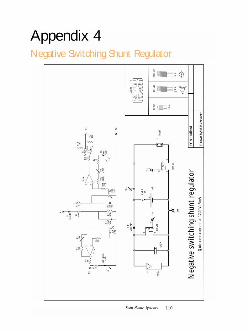
Appendix 4Negative Switching Shunt Regulator
110Solar Home Systems
Neg
ativ
e sw
itchi
ng s
hunt
reg
ulat
orQ
uies
cent
cur
rent
at
12,0
0V.:
5mA
ECN
Hol
land
Dra
wn
by: M
.R.V
erva
art
g
sd
IRF
540
MBR
745
k a
BC54
7
g d
s
c b
e
++
++
_
__
_
+
Gnd
1LM
324
12 3
+ -+–
765
ec
b
R9
1K
R8
1K
R12 1K
P2 20K
'LV
D'
LED
red
'L
VD
'D
38V 1W
R2
100K
C1
10uF
50V.
P1 20K
'HV
D'
R1
100K
R3 1k
D4
1N41
48
R4
1K
R5
1M
IC1a
IC1b
R6
1K
R7
1K
LED
gre
en'H
VD
'
R10
320K
27K
R13
12K
T3
BC54
7B
P4 200K
P3 2M
R11
V+
T2
T1
0V.
MO
Vm
od.
bat
IRF5
40g s
d
V+
+ –lo
ad
T1
T2 0V
.
IRF5
40
D1
MBR
745
FUSE
18A
++
g
sd

Appendix 5
Negative Sw
itching Shunt Regulator with E-Fuse
111Solar H
ome System
s
9-1998ECN Holland
Drawn by: M.R.Vervaart
MOV
mod.bat
IRF540
gs
d
g
s d
V+
+
–load
T1
T2
0V.
RshuntIRF540
V1
D1MBR745
FUSE 28A
Negative switching shunt regulator with E-fuseQuiescent current at 12,00 V.: 4mA.
IRFZ 540 MBR 745
k a
BC547
g d s
gs
d
1LM324
+
+
+
+
_
__
_
+
Gnd
c b e
+
+
12
3
R91K
R8 1K
R121K
P220K
LED red'LVD'
V+
T2T1
0V.
D38V
1W
R2100K
C110uF50V.P1
20K
R1100K
R31K
D41N4148
R410
R51M
+
– +
–
IC1aIC1b7 6
5R61K
R71K
LED green'HVD'
R10320KR11
27K
R1324K
T4BC547B
C2100uF50V. ++
++
LED yellow'Current-
limit'R1510K
R14100k
C310uF50V.
C447uF/50V.
R19320K
P5 10K'A-limit' 0...10A.
R17 2M
R181K
D61N4148
+
–+
–
IC1dIC1c
V1
R20 47K
D7 1N4148
R16 24KT3
BC547B
1412
13
810
9
P4200K
P32M

Appendix 6Positive Switching Charge Regulator with E-Fuse
112Solar Home Systems
Posi
tive
switc
hing
reg
ulat
or w
ith c
urre
nt li
mite
r 5
A s
yste
m, q
uies
cent
cur
rent
5m
A
1LM
324
++
++
_
__
_
+ Gnd
IRF9
Z34
NM
BR 1
045
k a
g d
s
gsd
10-1
998
ECN
Hol
land
Dra
wn
by: M
.R.V
erva
art
MO
V
Bat
IRF9
Z34
N
gsd
gs d
V+
+ –lo
ad
T2
T1
0V.
D1
MBR
1045
FUSE
28A
IRF9
Z34
N+
+
Mod
.
Rsh
unt
V1
1
23
R9 1K
R10
10K
P2 20K
LED
red
'LVD
'
V+
Z1
8V0
R4 120K
C1
10uF
50V.
P1 20K
R612
0K
R5 1K
D5
1N41
48
R11
10K
R8 1M
+-+ -
IC1a
IC1b
76 5
R1 10K R2 1K
LED
gre
en'H
VD'
R3 200K
R7 10K
C2
100u
F50
V.+
+
P3 100K
P4 2M
11
4T
2
0V.
+
LED
yel
low
'Cur
rent
-lim
it'
R13
120K
R17
100k
C3
10uF 50V.
C4
+
10uF
/50V
.
R21
320K
P5 1
0K'A
-lim
it' 0
...10
A.
R19
2M
R20
1K
D2
1N41
48
+ –
+–
IC1d
IC1c
V1
R18
47K
D3
1N41
48
T3, T
4BC
547B
1412 13
8109
R22
10k
R14
190K
R15
120K
R16
120K
R23
10K
T1
R24
10K

113Solar Home Systems
Appendix 7200VA HF Full-Bridge InverterThe schematic in this appendix was originally intended to be printed on a much larger paper size.To view the detail more clearly, use the magnifying function in Acrobat Reader.

Appendix 8HF Full-Bridge Inverter Using IntegratedCircuit HIP4082
114Solar Home Systems

115Solar Home Systems

116Solar Home Systems

Appendix 9Introduction to Light and Lighting
Color and wavelengthVisible light is electromagnetic radiation in wavelengths for which the human eye is sensitive, that is, in the
range of 400–800 nanometers (nm).1 Sensitivity is low for deep blue–colored short wavelengths. It peaks inthe green at about 555 nm, and is low in the deep red at around 800 nm. An approximation of the sensitivitycurve of the human eye is presented in figure A10.1. It shows the relative sensitivity as a function of wave-length. The maximum of 100 percent is reached at a wavelength of 555 nm.
Light output of a lamp: luminous flux[[H2]]Since light is a form of energy, it is possible to express the light output of a lamp in units of power: watts.
However, this would give very little information about the visual impression of the light. To quantify theamount of visible light, the spectral intensity of the light (see figure A2.5) is multiplied with the eye sensitivitycurve (see figure A10.1) and added to obtain the luminous flux (Lu) in lumens (lm).
Efficiency of lamp or luminaire: Luminous efficacyThe efficiency with
which a lamp produceslight in the visible spec-trum is defined as the lumi-nous flux per unit ofpower: lumens per watt.
Luminousintensity
The amount of lightemitted in a certain direc-tion is the luminous inten-sity (Li). It is defined as theluminous flux per steradi-an, with the unit candela(cd). Since there are 4 pi steradians in a sphere, the relation between the average luminous intensity Liav andthe luminous flux of light source is as follows:
Lu = 4 * pi * Liav
117Solar Home Systems
1 One nanometer is one-billionth (10–9) of a meter.
0
0.1
0.2
0.3
0.4
0.5
0.6
0.7
0.8
0.9
1
400
500
600
700
800
rele
tive
sens
itivi
ty [%
]
wavelength (nm)
Relative sensitivity of human eye compared to maximum at 555 nm

IlluminanceA measure of how well a surface is lit is presented by the illuminance. It is defined as the luminous flux per
unit of surface area. The unit is lux. 1 lux = 1 lumen per square meter. The illuminance E at a point with a dis-tance d from the light source can be expressed as a function of the angle a between the beam of light and thesurface:
E = (Li/d2)*sine(a)
Illuminous efficacyAnalogous to the luminous efficacy, the illuminous efficacy is a measure of the efficiency with which a light
source illuminates a surface. It is presented in lux per watt.
Correlated Color TemperatureThe color appearances of the light source are expressed in the correlated color temperature (CCT). When the
CCT is below 3,300 Kelvin, the light appears reddish. This is called warm white. With a CCT higher than5,300 Kelvin, the light appears bluish. An intermediate appearance occurs with a CCT between 3,300 and5,300 Kelvin.
Color rendering
Definition from Rural Lighting:A Guide for Development Workers.
The color of an object appears to differ when illuminated by different light sources. Color rendering is thedegree to which the colors of surfaces illuminated by a given light source conform to those of the same sur-faces under a reference. It is presented as a percentage. Good color rendering (80–90 percent) is achieved withincandescent lamps or fluorescent tubes with triphosphor coating. Moderate color rendering (60–80 percent)is achieved with standard fluorescent tubes.
118Solar Home Systems

Appendix 10Equipment Needed for Practical Part of the Training Course
119Solar Home Systems
During the hands-on training, locally produced bal-ance of system (BOS) components will be testedaccording to the local standards. After that, researchwill be done on how to improve the “weak spots” inthe design. The manual provides various solutions forproblems you might encounter in practice.
For the practical part, some basic equipment will benecessary to do proper measurements and to modifythe electronics thereafter. In the ideal case, the workcan be done in an electronic research and develop-ment laboratory. Depending on the number of partici-pants, you can form multiple groups. In this way, youcan run several tests simultaneously and use the timemore efficiently. The critical factor is the limitedamount of hardware available.
The basic materials needed are charge regulators, flu-orescent lamps inverters (FLIs), and DC-AC convert-ers. Following are the recommendations:
Charge regulators
At least two samples of one type of a locally manu-factured charge regulator.
Two digital multimeters. Power-supply 0–30 V, 0–10 A (depending on the
maximum current rating of the charge regulator). Trimmable load 0–10 A (depending on the maxi-
mum current rating of the charge regulator).
In the case of a pulse-width modulation (PWM)charge regulator, an oscilloscope is recommended.
Fluorescent lamps inverters (FLIs)
At least two samples of one type of a locally manu-factured FLI.
One or two digital multimeters. Digital oscilloscope with computer connection or
floppy drive (to measure electrical efficiency and tohandle pictures in the final report of the course).
A personal computer with Excel and Word.
DC-AC converters
Power-supply 0–20V, 0–20A (depending on themax. power rating of the DC/AC-inverter)
For the rest the above listed materials will be usedfor these measurements
General
The locally applied standards for these three BOScomponents, when available.
Two soldering irons and soldering material. Some stock of standard electronic components
(resistors, capacitors, transistors, some powerMOSFETs p- or n-type, and material for makingtransformers for FLIs).
These basic materials can be shared by the differentgroups. For example, two or three multimeters andan oscilloscope can be used by all groups.

Appendix 11Training Program Evaluation
Mitigating Global Climate Change through the Developmentof a Quality Process Infrastructure for Renewable Energy(Quap-PV)
Please complete the questionnaire, and hand in before leaving.
Optional: If you do not want to give your name, you do not need to. The main priority is to get your feedback.
Name: _ _ _ _ _ _ _ _ _ _ _ _ _ _ _ _ _ _ _ _ _ _ _ _ _ _ _ _ _ _ _ _ _ _ _ _ _ _ _ _ _ _ _ _ _ _ _ _ _ _ _ _ _ _ _ _ _ _ _ _ _ _ _ _ _ _ _ _ _ _ _ _ _ _ _ _ _ _ _ _ _ _ _ _ _ _ _ _ _ _ _ _ _ _ _ _ _ _ _
Organization: _ _ _ _ _ _ _ _ _ _ _ _ _ _ _ _ _ _ _ _ _ _ _ _ _ _ _ _ _ _ _ _ _ _ _ _ _ _ _ _ _ _ _ _ _ _ _ _ _ _ _ _ _ _ _ _ _ _ _ _ _ _ _ _ _ _ _ _ _ _ _ _ _ _ _ _ _ _ _ _ _ _ _ _ _ _ _ _ _ _ _ _ _ _ _ _ _ _ _
Phone: _ _ _ _ _ _ _ _ _ _ _ _ _ _ _ _ _ _ _ _ _ _ _ _ _ _ _ _ _ _ _ _ _ _ _ _ _ _ _ _ _ _ _ _ _ _ _ _ _ _ _ _ _ _ _ _ _ _ _ _ _ _ _ _ _ _ _ _ _ _ _ _ _ _ _ _ _ _ _ _ _ _ _ _ _ _ _ _ _ _ _ _ _ _ _ _ _ _ _
Fax: _ _ _ _ _ _ _ _ _ _ _ _ _ _ _ _ _ _ _ _ _ _ _ _ _ _ _ _ _ _ _ _ _ _ _ _ _ _ _ _ _ _ _ _ _ _ _ _ _ _ _ _ _ _ _ _ _ _ _ _ _ _ _ _ _ _ _ _ _ _ _ _ _ _ _ _ _ _ _ _ _ _ _ _ _ _ _ _ _ _ _ _ _ _ _ _ _ _ _
Design and Modification of BOS Components
ContentsGood Average Bad
Contents of the course O O O O OUsefulness of the course O O O O O
Training materialGood Average Bad
Quality of the training manual O O O O OQuality of the overhead sheets O O O O OUsefulness of the training manual O O O O OCompleteness of the training manual O O O O O
120Solar Home Systems

Which topics in the manual could be left out? ____________________________________________________
Which topics were missing in the manual? ______________________________________________________
Which topics in the manual could be briefer? ____________________________________________________
Which topic in the manual could be expanded? __________________________________________________
Exercises (hands-on training)
Did you participate in the hands-on training? Yes O No O
If yes, did it give a good insight into how to design and modify BOS electronics? Yes O No O
If no, what can be added to the hands-on training? ______________________________________________
________________________________________________________________________________________
If you participated in the hands-on training, how good was it?Good Average Bad
O O O O O
Presentation of the Lectures
Good Average BadHow well did the instructor present
the material? O O O O O
How well did the instructor respond to questions? O O O O O
How well did the instructor involve the participants? O O O O O
121Solar Home Systems

OrganizationGood Average Bad
How was the information you received before the training course? O O O O O
How were the arrangements of your participation? O O O O O
How was the training room? O O O O
How were the accommodations? O O O O O
How was the food? O O O O O
Additional comments(suggestions for improvement/criticism)
________________________________________________________________________________________
________________________________________________________________________________________
________________________________________________________________________________________
________________________________________________________________________________________
________________________________________________________________________________________
________________________________________________________________________________________
________________________________________________________________________________________
________________________________________________________________________________________
________________________________________________________________________________________
________________________________________________________________________________________
122Solar Home Systems

123Solar Home Systems
Appendix 12Sample Checklist
Test Report for Low Voltage DC Lights for Solar Home Systems Project No.:
Manufacturer: Client: Name of unit:
Type of Unit:Type Number :Serial number:
Tested by: M van Leeuwen Test Batch Number:Date:Sheet of
Description of testOkay/Fail/ Value Comments
1.General Inspection
(C-G 8) Visual InspectionC-G 9.1) Funtional Test DC range 10 Vdc -16Vdc
or Manufacturers Spec.2.4 Visual Inspection Terminals, Safety Earth2.5 Visual Inspection Creepage2.9 Visual Inspection Accidental Contact to live parts
2.Safety2.1C-G 9.) Insulation resistance 48hr @ 91%-95% RH, 20-30 Celsius > 2 M Ohm2.2 Dielectric Strenght 50 Hz @ 500Vac No Flashover2.3 Pulse Voltage 16Vdc + 3 x 16Vpeak,10ms2.7 Fault condition test
Abnormal Conditions 2.8.1 Lamp removal 1 Hour @ 16Vdc2.8.2 Lamp Fai lure Filament resistor for 1 hr ( IEC 0081)2.8.3 Reverse Polarity Blocking Diode
3.Performance Tests3.1 Cold Start 12Vdc +/- 10% @ 10 up to 35 degrees Celsius
Operation 12Vdc +/- 10% @ 10 up to 50 degrees Celsius3.2 Open circuit lamp Voltage @ 16Vdc Vpk3.3 Lamp Current @ 12Vdc mA3.4 Inom. @ 12Vdc mA3.5 Max. Curent Electrode Supply. @ 12Vdc mA3.6 Lamp waveform @ I nom @ 12Vdc3.7 see functional test
Vdc input A WattInput power P @ 10Vdc 10
3.8 Input power P @ 16Vdc 163.9 Luminous Efficacy @ 2000 hr burnning period
4.Endurance Test4.1 100 hr. burn-in Luminous Flux
4.2 10,000 Switching Test 60 sec On,120 sec. Off
5.EMC See Separate test report
Comments

124Solar Home Systems
Test Report for Low Voltage DC PV Charger Controllers for Solar Home Systems Project No.:
Manufacturer:
Client: Name of unit:Type of Unit:Type Number :Serial number: Number of samples:
Tested by: Test Batch Number: Date:Sheet
Documentation Comments4.1.1, 4.1.2, 4.1.3 Yes No
* Installation, Operat ing and trouble shooting instructions* Waranty* Condit ions of surroundings* Physical properties of the charge regulator* Electrical properties of the charge regulator
6. Marking* Maximum Module & Load Current* Nominal voltage* Polarity display* Labeling displays* Fuse values
8.Electrical Parameters 12V. 24V.8.1 Nominal Voltage
8.2 (PWM, Shunt or series)
Working principle Voltage controlSOC algorithm
+ -Switching polarity
Cenelec Y N 8.3 Switching thresholds Imod=25% HVD 2.30 V/cell
HVR 2.25 V/cellIload=25% LVD 1.90 V/cell
LVR 2.10 V/cell
8.5 Status Indicator Display
Visual Inspection9. O.K. Comments
Damage to the case, on terminals or displaysQuality of caseQuality of Electronic systemQuality of wiring
10.1 Function testEnd of charge voltagesHVD Imod. 6A VHVR V
I load: 0A 3A 4,0 ALVDLVR
Gassing voltage (NP = Not present) np
Performance test V at: Quiescent current mA.Voltage drop Module-Battery Imod. 6A V. Voltage drop Battery-Load Iload 4.08 A V.
Y NVoltage drop compensationI f yes, dV Battery terminal / Treshold controller < 100mV

125Solar Home Systems
Abbreviations and Special TermsAC Alternating current—flow alternates current in cycles called Hertz (Hz).ADC Analog digital conversionBallast High-frequency inverter, used for driving a fluorescent lamp.B-H Created flux density (B) versus field intensity (H)BJT Bipolar junction transistorBOS Balance of systemCFL Compact fluorescent lampCMOS Complementary metal-oxide semiconductorDC Direct current—current flows in only one directionD.C. Duty cycleEEPROM Electric erasable programmable read only memoryelco Electrolytic capacitorECN Netherlands Energy Research Foundation
(Energieonderzoek Centrum Nederland)EMC ElectromagneticEMF Electromagnetic forceEMI Electromagnetic inductanceESR Electrostatic resistanceFET Field-effect transistorFL Fluorescent lampFLI Fluorescent lamp inverterGTO Gate transmission openerHVD High-voltage disconnect—the instant in time when the module is disconnected from the system
in order to stop battery chargingHVR High-voltage reconnect—the instant in time when the module is reconnected to the systemIC Integrated circuitIEA PVPS International Energy Agency—Photo Voltaic Power SystemsIEC International Electrotechnical CommissionIGBT Insulated gate bipolar transistorLC Circuit with an inductance (L) and capacitor (C)L-C filter Filter, based on an inductor and a capacitorLED Light-emitting diodeLRC Circuit with a resistor, inductor, and capacityLVD Low-voltage disconnect—the instant in time when the load is disconnected from the system
because of a low batteryLVR Low-voltage reconnect—the instant in time when the load is reconnected to the system and ener-
gy use is enabledMOSFET Metal-oxide semiconductor field-effect transistorMOV Metal-oxide varistorNOCT Nominal operating cell temperatureopamp Operational amplifierPCB Printed circuit boardPV PhotovoltaicPW Pulse width

PWM Pulse-width modulationQNOT The inverted output of a flip-flopRC Circuit with resistance and capacityRMS Root mean squareSHS Solar home systemSLI Starting, lighting, ignition (battery)SOC State of charge (of the battery)STC Standard test conditionsTVS Transient voltage surpressorVCO Voltage control oscillatorVHF Very high frequencyVR Valve regulated (batteries)VSI Voltage-source inverter
Crest factor = (Peak voltage) / (RMS voltage)Duty cycle = (on-time/off-time) x 100%Electrical efficiency = (Output power) / (input power) x 100%
Units of MeasureAmpere (A) The standard unit for measuring the strength of an electric current.Ampere-hour The standard unit for measuring the quantity of electricity, equal to the flow of a current of oneampere for one hour.Amplitude The extreme range of a fluctuating quantity, as an alternating current, generally measured from theaverage or the mean to the extreme.Celsius (ºC) A scale on which 0º is the freezing point and 100º is the boiling point of water.Coulomb (C) Charge transported through a conductor by a current of one ampere flowing for one second.Hertz (Hz) The international unit of frequency, equal to one cycle per second.Joule The amount of work done by one newton acting through a distance of one meter.Kilohertz (kHz) 1,000 hertz.Lumen (lm) A unit of measure for the flow of light, equal to the amount of flow through a unit solid anglefrom a uniform point source of one candela.Lux (lx) A unit of measure equal to one lumen per square meter or to the illumination of a surface uniformlyone meter distant from a point source of one candela.Newton (N) Force that imparts to a mass of one kilogram an acceleration of one meter per second per sec-ond.Ohm ( ) Electrical resistance, measured in volts per ampere.Volt (V) The unit of electromotive force between two points in an electric field that requires one joule of workto move a positive charge one coulomb from the point of lower potential to the point of higher potential.Voltage Electromotive force expressed in volts.Watt (W) The unit of electrical power equal to one joule per second or to the power developed in a circuit bya current of one ampere flowing through a potential difference of one volt.Watt-peak (Wp) At a solar radiation of 1,000 W/m2, at 25°C and with an air mass of 1.5, 1 watt-peak deliv-ers 1 W energy.Watt-hour (Wh) A unit of electrical energy or work equal to 1 watt acting for 1 hour, or 3,600 joules.
126Solar Home Systems

ReferencesAndersson, Bo, Catella Generics, and Staffan Ulvonas. Battery Guide for Small
Stand Alone Photovoltaic Systems. IEA PVPS Task III.Cabraal, Anil, Mac Cosgrove-Davies, and Loretta Schaeffer. 1996. Best Practices
for Photovoltaic Household Electrification Programs; Lessons from Experiences inSelected Countries. Technical Paper No. 324. Washington, D.C.: World Bank.
ECN. “Rural Lighting Services: A Comparison of Lamps for Domestic Lightingin Developing Countries.” Petten, Netherlands: ECN.
ELV GmbH. 1993. 200Watt PowerInverter. Holland: Elektuur uitgeversmij.Gerken, K., and D. Welsch. February 1997. A Pulse-Width Modulated High
Reliability Charge Controller for Small Photovoltaic Systems. Report SAND97-0329. Albuquerque, New Mexico: Sandia National Laboratories.
Intersil. 1996. A DC–AC Isolated Battery Inverter Using HIP4082. Palm Bay,Florida, U.S.A.: Application note at http://www.intersil.com.
Khan, Hasna J., Rezwan Khan, and Salma Khatun. 1998. Optimal Design of DCLuminaires for Solar PV Applications. Final draft. Prepared for the World Bank.
Louineau, Jean-Paul, Mobido Dicko, Peter Fraenkel, Roy Barlow, and VarisBokalders. 1994. Rural Lighting: A Guide for Development Workers. Stockholm:IT Publications in association with the Stockholm Environment Institute.
Mohan, Ned, Tore M. Undeland, and William P. Robbins. 1995. PowerElectronics: Converters, Applications and Design. New York: John Wiley andSons.
Nieuwenhout, F. D. J., P. J. N. M. van de Rijt, and E.J.Wiggelinkhhuizen. 1998.Rural Lighting Services: A Comparison of Lamps for Domestic Lighting inDeveloping Countries. Petten, the Netherlands: Netherlands Energy ResearchFoundation (ECN).
OTTI Technologie-Kolleg. May 1999. Erstes Fachforum WiederaufladbareBatteriesysteme. Regensburg, Germany: OTTI.
Petrus, Tri Bakti. 1997. Perancangan DC Ballast Inverter. Jakarta, Indonesia: PTLen.
Séguier, Guy, and Francis Labrique. 1993. Power Electronic Converters: DC–ACConversion. Berlin and Heidelberg: Springer Verlag.
127Solar Home Systems

128Solar Home Systems