solid state frequency multipliers at sub-millimeter wavelength
TRANSCRIPT
23RD INTERNATIONAL SYMPOSIUM ON SPACE TERAHERTZ TECHNOLOGY, TOKYO, 2-4 APRIL 2012 1
Solid State Frequency Multipliers at Sub-MillimeterWavelength Using European Schottky Technology
J. Treuttel, F. Yang, M. Benzazaa, A. Maestrini, J. V-Siles, H. Wang, H.Sanghera, B.Alderman.
Abstract—We report upon the design of solid state frequencymultipliers : a 380 GHz single-chip doubler, a 300 GHz single-chip tripler and a 300 GHz power combined dual-chip tripler.They are all designed with a dedicated model of europeanintegrated Schottky diodes and in the triplers case with theiron-chip capacitor for bias connection. A dedicated technology isdevelopped in order to enhance device performance, in particularimprove the power handling capabilities which vary from 50mW for the single chip 380 GHz doubler up to 400 mW for the300 GHz dual-chip tripler. The circuits are under fabrication atSTFC-RAL.
Index Terms—Frequency multipliers, Schottky diode, Doubler,Tripler, Power-combining, Sub-millimeter wave.
I. INTRODUCTION
The terahertz spectrum is now willing to be fully exploitedto enrich applications that span the physical, biological, andmedical sciences. One of the remaining technology challengeat THz frequencies is to generate conveniently useful amountsof power. Schottky diodes based solid-state devices stand asfirst candidates where compact, non-cryogenic and efficientsources are needed. Therefore the Millimeter-wave IntegratedDiode and Amplifier Source (MIDAS) project aims at devel-oping MMIC power amplifiers and Schottky varactor diodecircuits using European technology. The primary objective ofthe program is to demonstrate a 125 mW source operating at270 - 300 GHz in conjunction with power combining technol-ogy. The designs of three last stage frequency multipliers usingon-chip capacitor and integrated Schottky diodes are proposedduring the first phase of the program and are presented in thisarticle: a single-chip 380 GHz doubler, a 300 GHz single-chip tripler, and a 300 GHz in-phase power-combined dual-chip tripler. We report on the design and performance of thesethree designs.
Manuscript received April 2, 2012. This work was supported by MIDASprogram within European commission Seventh Framework Programme FP7-242334.
J.Treuttel and M. Benzazaa are with Observatoire de Paris, LERMA, 75014Paris, FRANCE.
F.Yang is with Observatoire de Paris, LERMA, 75014 Paris, FRANCE, vis-iting scientist from State Key Lab of Millimeter Waves, SouthEast University,CHINA.
A.Maestrini is with Observatoire de Paris, LERMA, 75014 Paris andUniversite Pierre et Marie Curie Paris 6, FRANCE.
J.V. Siles was with is with Observatoire de Paris, and now with JetPropulsion Laboratory, California Institute of Technology, Passadena CA91109, USA.
H. Wang, H. Sanghera and B.Alderman are with Rutherford AppletonLaboratory, STFC, Didcot, OX11 0QX, UK.
A. Towards a high frequency and high power MMIC fabrica-tion process
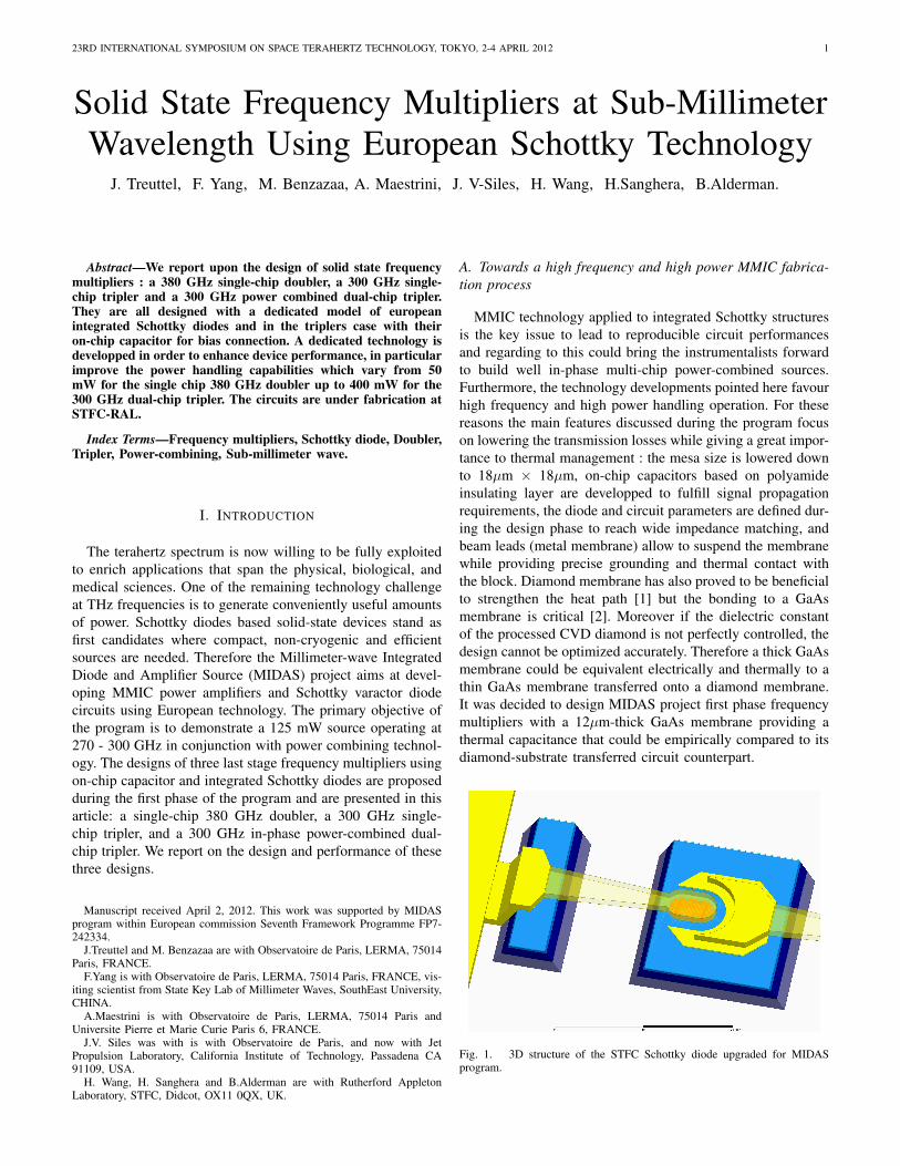
MMIC technology applied to integrated Schottky structuresis the key issue to lead to reproducible circuit performancesand regarding to this could bring the instrumentalists forwardto build well in-phase multi-chip power-combined sources.Furthermore, the technology developments pointed here favourhigh frequency and high power handling operation. For thesereasons the main features discussed during the program focuson lowering the transmission losses while giving a great impor-tance to thermal management : the mesa size is lowered downto 18µm × 18µm, on-chip capacitors based on polyamideinsulating layer are developped to fulfill signal propagationrequirements, the diode and circuit parameters are defined dur-ing the design phase to reach wide impedance matching, andbeam leads (metal membrane) allow to suspend the membranewhile providing precise grounding and thermal contact withthe block. Diamond membrane has also proved to be beneficialto strengthen the heat path [1] but the bonding to a GaAsmembrane is critical [2]. Moreover if the dielectric constantof the processed CVD diamond is not perfectly controlled, thedesign cannot be optimized accurately. Therefore a thick GaAsmembrane could be equivalent electrically and thermally to athin GaAs membrane transferred onto a diamond membrane.It was decided to design MIDAS project first phase frequencymultipliers with a 12µm-thick GaAs membrane providing athermal capacitance that could be empirically compared to itsdiamond-substrate transferred circuit counterpart.
Fig. 1. 3D structure of the STFC Schottky diode upgraded for MIDASprogram.

23RD INTERNATIONAL SYMPOSIUM ON SPACE TERAHERTZ TECHNOLOGY, TOKYO, 2-4 APRIL 2012 2
B. 380 GHz Doubler design
The circuit design of a 380 GHz fixed-tuned MMIC doubleris based on the balanced topology presented in [3]. The inputfrequency was chosen according to the second stage doubleroutput issued separately in this proceedings, which features a190 GHz single-waveguide in-phase dual-chip doubler basedon [4] and that is expected to provide between 50 to 100 mWdepending on its input power handling capabilities (200 to400 mW at W band) and on the first stage power amplifiersefficiency also developped during the program 1. The 380GHz doubler features an anti-serie set of four planar Schottkydiodes integrated within the passive microstrip circuit onto a12-µm thick GaAs membrane. The circuit geometry preventsthe input fundamental signal from leaking into the output andalso prevents the output second harmonic signal from leakinginto the input waveguide. Moreover, the reduced height inputwaveguide cut off the input signal TM11 mode for a moreefficient coupling to the diodes. A stepped impedance filtersection at the opposite end of the circuit is used as a DC biasvoltage path and avoid the leakage of the second harmonicthrough this port. Therefore on-chip capacitor is not necessaryfor this particular design. The input and output waveguides,the microstrip channel and the DC bias connector sockets aremilled into two split-waveguide metal blocks. The position ofthe input backshort, the diodes geometry, the input stub nearthe diodes and the output probe were optimized to reach awide impedance matching over the input frequency band.
Fig. 2. Picture of the fully optimized 380 GHz doubler placed inside thewaveguide cavity.
The methodology used for the design uses a combinationof linear/non-linear circuit simulations (Agilent ADS) and3D electro-magnetic simulations (Ansoft HFSS). Firstly, astandard diode model from the ADS library was implementedtogether with its close 3D passive environnement (diode cell),plus ideal input and output matching networks. During thissimulation, the anode zero junction capacitance and the diodecell geometry (anodes positions, input channel width andinput stub length) were optimized using the harmonic-balance
1by Radiometer Physics Gmbh
routine for 50 mW input power in order to reach optimumefficiency (see Fig. 3). The corresponding diodes impedancesare ZIN = 13 - j. 89 Ω, and ZOUT = 33 + j. 28 Ω respectivelyat input and output frequencies, with a bias voltage of-5 V. These embedding impedances values as a functionof frequency were exported into Z-files which were usedas a first input of the linear optimization. Secondly, eachof the transition in the circuit including step impedances,coupling probes and waveguide transitions were simulatedwithin the 3-D electromagnetic environment with appropriateboundaries, waveports assignment and de-embedding planes.The simulation outcomes (2-D S-parameter matrices andtheir attenuations, impedances and permittivity values atcentral guided frequencies) were used a second input ofthe linear optimization. During this optimization step, thematching network was simulated with the ”S-parameter” and”Optim” routines of ADS in order to find optimum lengthsof the circuit. The diode impedance frequency set is accessedthrough a ”DAC” file component and the S-parameter matrixthrough ”Data-item” component with a number of ports thatcorresponds to the ports defined in the 3D EM simulation. Afirst set of circuit dimensions was found by optimizing thecoupling between diodes and output port, which transmissionmagnitude should reach a maximum of 1/
√4 = 0.5 . The
center pad, the output probe and the DC bias filter wereoptimized for wideband impedance matching. A secondset of value was found by refining the optimization withthe harmonic balance routine. Few iterations between thelinear and the nonlinear optimizations were performed untilthe emergence of acceptable performance. Finally, the eachsection values found during the previous steps were feedback in HFSS to build the full doubler circuit structure asshown in Fig. 2. Its performance were then checked usingthe nonlinear harmonic balance routine.
Fig. 3. Predicted performance of the 380 GHz doubler, the dot curve is theefficiency of the diode cell with ideal matching network, the full line is thefully optimized circuit as illustrated in Fig.3.
The electrical parameters of the STFC-RAL Schottky diodemodel considered in the simulations are a series resistance Rs= 7.5 Ω, an intrinsic zero voltage junction capacitance of Cjo= 15.7fF, a saturation current Isat = 150 fA, an ideality factor= 1.3 and a built-in potential Vbi = 0.85 V. This design wasoptimized for 50 mW of input power and -5 V bias voltage.The diodes anode area is 2.2µm × 4.5µm. Fig.3 shows theestimated efficiency of the doubler. Expected Performancesgives 20% efficiency over 10% bandwidth.

23RD INTERNATIONAL SYMPOSIUM ON SPACE TERAHERTZ TECHNOLOGY, TOKYO, 2-4 APRIL 2012 3
C. 300 GHz Tripler designs
1) Tripler single chip design: The tripler features six in-tegrated GaAs Schottky diodes in a balanced configurationbased on [5]. The on-chip capacitor is integrated within themembrane according to STFC-RAL fabrication process. Thisintegration provides a precise DC connection, but also allowsa better control of the bias port, which is shifted away fromthe diode cell and which dimensions are chosen to avoidany leakage of the output signal. A notch in the bias line ismandatory to meet the photolitographic process requirementbut has negligible impact on the circuit performance. Theinput and output waveguide dimensions cut off respectivelythe input signal TM11 mode and the second idler harmonicTE10 and TM11 modes. A detailed explanations of the designmethodology of the circuit are given in [5]. The optimizationis performed using 3D electromagnetic codes alike for thedoubler, but the methodology slighty differs from the 380GHz doubler as the initial diode cell optimization includesthe diodes plus a section of the chip-channel and its on-chipcapacitor. The optimum diode junction capacitance and biasvoltage were determined at the same time to reach highestefficiency and power handling as possible. When the triplercircuit was achieved, then the input waveguide network hadto be tuned to reach wide-band performance. This step wasdone with a linear optimization that allow an easy manualtuning of the matching network circuit. Firstly the triplerdiodes ideal impedances were computed with the harmonicbalance routine with ideal matching networks to converge toan optimum efficiency. The corresponding set of impedancesare ZIN = 32 -j 80 Ω, and ZOUT = 24 + j 44 Ω respectivelyat input and output frequencies. The idler impedance is closeto zero that confirms that the power is ideally transposed tothe third harmonic. Secondly, the input and output matchingnetwork was divided into several individual sections, and thediscontinuous parts between them were simulated in HFSS.The resulting S-parameter matrices and the diodes optimumembedding impedances were then utilized to determinate afirst set of circuit dimensions using the linear simulator inADS by optimizing the coupling between diodes and outputport. The optimisation goal of the port-to-port matching isthe transmission from the input port to each of the 6 anodeswhich maximum magnitude were 1/
√6 = 0.4 . When the non-
linear matching had achieved the desired coupling with anoptimal tuning, the circuit was simulated with the harmonicbalance routine to check the tripler coupling efficiency, globalefficiency and output power.The electrical parameters of the Schottky diode model con-sidered in the simulations are a series resistance Rs = 5.4Ω, an intrinsic zero voltage junction capacitance of Cjo =26 fF, a saturation current Isat = 100 fA, an ideality factor= 1.2 and a built-in potential Vbi = 0.85 V. The bias valueapplied to the 6 diodes in series is 13 V. Expected simulatedperformances gives between 5% and 10% percent efficiencyover 17% bandwidth with 200 mW of input power as shownin Fig.4. The block and tripler are being fabricated at STFC
Fig. 4. Simulation results of the Single Chip 300GHz Tripler : Output powerwith 200 mW of input power.
with a variation of two different epilayer doping densities :1.10−17cm−3 and 3.10−17cm−3 and with the corresponding30µm2 and 17µm2 anodes area, with ± 15% bracketing.
Fig. 5. Single chip 300GHz tripler mounted in half part of the split blockwith its input waveguide matching network.
2) Tripler power-combined design: The topology used forthis design is similar to the one presented in [6], but with biasports reported to the other side of the input waveguide thatmakes possible to have in-line matching network waveguidetransitions. This solution bypass the need for curvatures inthe input waveguide and avoid unwanted phase shift (andimbalance) between the input port and the diodes of thetwo symmetrical chips. As for the doubler and tripler single-chip designs, the matching network optimization consists in acombinaison of linear / non linear simulations that converge toa final configuration. The ideal diode impedance set used in thelinear simulation was the one found for the single chip tripler.The optimisation goal of the port-to-port matching was thetransmission between the input port to each of the 12 diodeswhich maximum magnitude was 1/
√12 = 0.28 . Preliminary
performances give above 6% efficiency over 15% bandwidth,therefore 25 mW to 35 mW of output power is expected overthe 270-315 GHz band with 400 mW input power.
II. CONCLUSION
Three multiplier designs are presented : a 380 GHz single-chip doubler, a 300 GHz single-chip tripler and a 300 GHz

23RD INTERNATIONAL SYMPOSIUM ON SPACE TERAHERTZ TECHNOLOGY, TOKYO, 2-4 APRIL 2012 4
Fig. 6. Picture of the fully optimized dual-chip 300GHz power combinedtripler.
Fig. 7. 300 GHz dual-chip power-combined tripler preliminary predictedoutput power efficiency compared to the single chip as given in Fig.6.
in-phase power-combined dual-chip tripler. These designs usecombinaison of linear/non linear optimization benches wheremanually tuning of the output and input matching networksis possible with dedicated transmission goals for respectivelythe output port to each of the diodes (doubler) and theinput port to each of the diodes (tripler). This methodologyhelps to widen drastically the performance bandwidth of thefrequency multipliers. These designs are implemented with amodel of MMIC diode circuits and their on-chip capacitordevelopped with STFC-RAL fabrication process for MIDAShigh frequency and high power requirements.
ACKNOWLEDGMENT
This work is supported by the European Community: FP7SPA.2009.2.2.01 Space Technologies.
REFERENCES
[1] C. Lee, J. Ward, R. Lin, E. Schlecht, G. Chattopadhyay, J. Gill,B. Thomas, A. Maestrini, I. Mehdi, and P. Siegel, A Wafer-LevelDiamond Bonding Process To Improve Power Handling Capability ofSubmillimeter-wave Schottky Diode Multipliers Microwave SymposiumDigest, 2009 IEEE MTT-S International, Boston, pp. 957 - 960, 7-12June, 2009.
[2] A. Y. Tang, E. Schlecht, G. Chattopadhyay, R. Lin, C. Lee, J. Gill,I. Mehdi, and J. Stake Steady-State and Transient Thermal Analysisof High-Power Planar Schottky Diodes in Proc. 21th Int. Symp. SpaceTerahertz Technol.,Tucson, USA, April 26-28, 2011
[3] N.R. Erickson Wideband High Efficiency Planar Diode Doublers,NinthInt’l Conference on Space THz Technology, pp.473-480,Pasadena,CA,1998.
[4] J. Siles, A. Maestrini, B. Alderman, S. Davies, H. Wang, J. Treuttel, E. Leclerc, T. Narhi, and C. Goldstein A single-waveguide in-phasepower-combined frequency doubler at 190 GHz, IEEE Microwave andWireless Components Letters, June 2011.
[5] A. Maestrini, J. Ward, J. Gill, H. Javadi, E. Schlecht, C. Tripon-Canseliet, G. Chattopadhyay and I. Mehdi, A 540-640 GHz High Effi-ciency Four Anode Frequency Tripler IEEE Transactions on MicrowaveTheory and Techniques, Vol. 53, No. 9, September 2005.
[6] A. Maestrini, J. Ward, C. Tripon-Canseliet, J. Gill, C. Lee, H. Javadi,G. Chattopadhyay, and I. Mehdi : In-Phase Power-Combined FrequencyTriplers at 300 GHz IEEE Microwave and Wireless Component Letters,Vol. 18, no. 3, pp. 218-220, March 2008.