solid-state lighting—a benevolent technologyschubert/reprints/2006... · 2006-11-08 ·...
TRANSCRIPT

INSTITUTE OF PHYSICS PUBLISHING REPORTS ON PROGRESS IN PHYSICS
Rep. Prog. Phys. 69 (2006) 3069–3099 doi:10.1088/0034-4885/69/12/R01
Solid-state lighting—a benevolent technology
E Fred Schubert1,2,3, Jong Kyu Kim1,2, Hong Luo1,3 and J-Q Xi1,3
1 The Future Chips Constellation, Rensselaer Polytechnic Institute, 110 Eighth Street, Troy,NY 12180, USA2 Department of Electrical, Computer, and Systems Engineering, Rensselaer PolytechnicInstitute, 110 Eighth Street, Troy, NY 12180, USA3 Department of Physics, Applied Physics, and Astronomy, Rensselaer Polytechnic Institute,110 Eighth Street, Troy, NY 12180, USA
E-mail: [email protected]
Received 6 July 2006Published 2 November 2006Online at stacks.iop.org/RoPP/69/3069
Abstract
Solid-state light sources are in the process of profoundly changing the way humans generatelight for general lighting applications. Solid-state light sources possess two highly desirablefeatures, which set them apart from most other light sources: (i) they have the potential to createlight with essentially unit power efficiency and (ii) the properties of light, such as spectralcomposition and temporal modulation, can be controlled to a degree that is not possible withconventional light sources such as incandescent and fluorescent lamps. The implications areenormous and, as a consequence, many positive developments are to be expected includinga reduction in global energy consumption, reduction of global-warming-gas and pollutantemissions and a multitude of new functionalities benefiting numerous applications. Thisreview will assess the impact of solid-state lighting technology on energy consumption, theenvironment and on emerging application fields that make use of the controllability affordedby solid-state sources. The review will also discuss technical areas that fuel continued progressin solid-state lighting. Specifically, we will review the use of novel phosphor distributions inwhite light-emitting diodes (LEDs) and show the strong influence of phosphor distributionon efficiency. We will also review the use of reflectors in LEDs with emphasis on ‘perfect’reflectors, i.e. reflectors with highly reflective omni-directional characteristics. Finally, we willdiscuss a new class of thin-film materials with an unprecedented low refractive index. Suchlow-n materials may strongly contribute to the continuous progress in solid-state lighting.
(Some figures in this article are in colour only in the electronic version)
This article was invited by Professor K Ploog.
0034-4885/06/123069+31$90.00 © 2006 IOP Publishing Ltd Printed in the UK 3069
3070 E F Schubert et al
Contents
Page1. Benefits of solid-state lighting 3071
1.1. Introduction to solid-state lighting 30711.2. Theoretical limits for efficiency 30711.3. Potential savings in energy and reduction of environmental pollution 30721.4. Solid-state lighting—beyond energy 3075
2. Highly efficient packaging configurations for phosphor-based white LED lamps 30762.1. Phosphor configurations in white LED lamps 30762.2. Whispering-gallery modes and diffuse reflector cups 30772.3. Simulation and experiment of phosphorescence efficiency 3080
3. Omni-directional reflectors for light-emitting diodes 30833.1. Reflectors for light-emitting diodes 30833.2. GaInN blue light-emitting diodes with omni-directional reflectors 30853.3. GaInN near ultraviolet light-emitting diodes with omni-directional reflectors 30893.4. AlGaInP light-emitting diodes with omni-directional reflectors 3091
4. Low-refractive-index optical thin films and their applications 30924.1. Low-refractive-index materials 30924.2. Oblique-angle deposition for films consisting of an array of nano-rods 30934.3. Low-refractive-index SiO2 30944.4. Optical multilayer structure with low-refractive-index SiO2 thin film 3095
5. Conclusions 3097Acknowledgments 3098References 3098
Solid-state lighting—a benevolent technology 3071
1. Benefits of solid-state lighting
1.1. Introduction to solid-state lighting
The very first solid-state light source was demonstrated approximately 100 years ago by HenryJ Round, a radio engineer who was searching for better crystal detectors for radio waves, whenhe accidentally discovered that light was being emitted from a man-made SiC crystal when acurrent flowed through the material. He saw a remarkably broad range of colours includingorange, yellow, green and blue. Over the last century, remarkable progress has been madein solid-state light-emitting devices, most particularly during the last 50 years. At the presenttime, technical advances in solid-state light sources are continuing unabated with sourcescontinuously becoming more powerful, brighter and more efficient.
A new era is dawning, the era of solid-state lighting in which the technical communityhas reason to believe that solid-state lighting will develop into a benevolent technology thatwill benefit humanity at large.
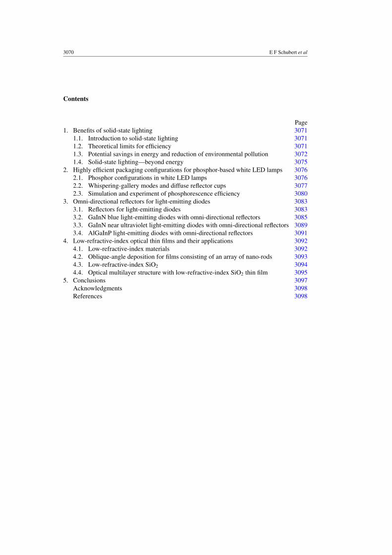
Three major benefits of solid-state lighting technology, shown in figure 1, can besummarized as follows: firstly, the inherent capability of solid-state sources to generatelight with high efficiency is resulting in giant energy savings. Secondly, potentially hugeenvironmental benefits are a result of the efficiency and durability of solid-state emitters,particularly light-emitting diodes based on inorganic semiconductors. Thirdly, solid-stateemitters allow one to control the emission properties with much greater precision, therebyallowing one to custom-tailor the emission properties for specific applications. Next, thesebenefits will be discussed quantitatively and in detail.
1.2. Theoretical limits for efficiency
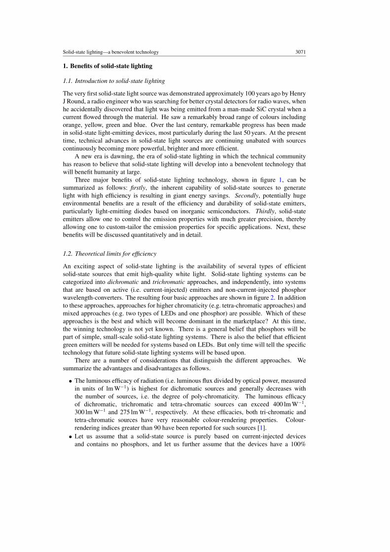
An exciting aspect of solid-state lighting is the availability of several types of efficientsolid-state sources that emit high-quality white light. Solid-state lighting systems can becategorized into dichromatic and trichromatic approaches, and independently, into systemsthat are based on active (i.e. current-injected) emitters and non-current-injected phosphorwavelength-converters. The resulting four basic approaches are shown in figure 2. In additionto these approaches, approaches for higher chromaticity (e.g. tetra-chromatic approaches) andmixed approaches (e.g. two types of LEDs and one phosphor) are possible. Which of theseapproaches is the best and which will become dominant in the marketplace? At this time,the winning technology is not yet known. There is a general belief that phosphors will bepart of simple, small-scale solid-state lighting systems. There is also the belief that efficientgreen emitters will be needed for systems based on LEDs. But only time will tell the specifictechnology that future solid-state lighting systems will be based upon.
There are a number of considerations that distinguish the different approaches. Wesummarize the advantages and disadvantages as follows.
• The luminous efficacy of radiation (i.e. luminous flux divided by optical power, measuredin units of lm W−1) is highest for dichromatic sources and generally decreases withthe number of sources, i.e. the degree of poly-chromaticity. The luminous efficacyof dichromatic, trichromatic and tetra-chromatic sources can exceed 400 lm W−1,300 lm W−1 and 275 lm W−1, respectively. At these efficacies, both tri-chromatic andtetra-chromatic sources have very reasonable colour-rendering properties. Colour-rendering indices greater than 90 have been reported for such sources [1].
• Let us assume that a solid-state source is purely based on current-injected devicesand contains no phosphors, and let us further assume that the devices have a 100%
3072 E F Schubert et al
Figure 1. Benefits enabled by solid-state light sources.
Figure 2. Approaches to solid-state lighting sources for general lighting applications.
electrical-to-optical-power-conversion efficiency. Then the luminous efficacy of radiationis equal to the luminous source efficiency (i.e. luminous flux divided by electrical inputpower, measured in units of lm W−1 as well).
• Devices containing phosphor wavelength-converters have advantages such as simplicity,colour stability and the need for only one power source. However, devices containingphosphors generally have a lower efficiency because of the unavoidable energy lossconcomitant with the wavelength-conversion of a photon from wavelength λ1 to λ2 withλ2 > λ1. The energy loss is particularly large for wavelength-conversion processes fromthe UV (400 nm) to the red (625 nm) where the loss is 36%.
• It is reasonable to assume that, given sufficient time and resources for development, the goalof reaching 50% of the theoretical maximum of the luminous efficiency is reasonable witha very good chance of being reached. Thus a luminous efficiency of 50% of 300 lm W−1,i.e. 150 lm W−1, is an optimistic yet reasonable long-term expectation for commercialsolid-state sources emitting high-quality white light.
There are many other aspects of solid-state devices that are highly relevant includingthe internal quantum efficiency of the active region, light-extraction, current-flow design,the minimization of resistive losses, electrostatic discharge stability, reliability, scalability toincrease the luminous flux per LED package and a low purchase price, to just name a few. Acomprehensive discussion of these important factors is not the intent of the authors and thereader is referred to the literature for a detailed discussion of these topics [2].
1.3. Potential savings in energy and reduction of environmental pollution
The total annual production of electrical energy in the US in 2004 was 14.98 × 10¹⁸ J =4161 TWh = 14.20 × 10¹⁵ BTU [3]. The US Department of Energy estimates that 22%of electricity is used for lighting [5]. Thus, the electrical energy generated annually in the
Solid-state lighting—a benevolent technology 3073
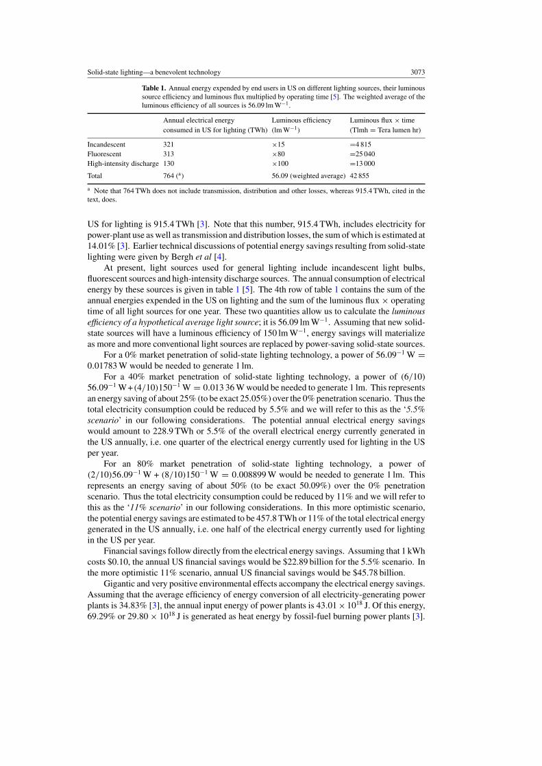
Table 1. Annual energy expended by end users in US on different lighting sources, their luminoussource efficiency and luminous flux multiplied by operating time [5]. The weighted average of theluminous efficiency of all sources is 56.09 lm W−1.
Annual electrical energy Luminous efficiency Luminous flux × timeconsumed in US for lighting (TWh) (lm W−1) (Tlmh = Tera lumen hr)
Incandescent 321 ×15 =4 815Fluorescent 313 ×80 =25 040High-intensity discharge 130 ×100 =13 000
Total 764 (a) 56.09 (weighted average) 42 855
a Note that 764 TWh does not include transmission, distribution and other losses, whereas 915.4 TWh, cited in thetext, does.
US for lighting is 915.4 TWh [3]. Note that this number, 915.4 TWh, includes electricity forpower-plant use as well as transmission and distribution losses, the sum of which is estimated at14.01% [3]. Earlier technical discussions of potential energy savings resulting from solid-statelighting were given by Bergh et al [4].
At present, light sources used for general lighting include incandescent light bulbs,fluorescent sources and high-intensity discharge sources. The annual consumption of electricalenergy by these sources is given in table 1 [5]. The 4th row of table 1 contains the sum of theannual energies expended in the US on lighting and the sum of the luminous flux × operatingtime of all light sources for one year. These two quantities allow us to calculate the luminousefficiency of a hypothetical average light source; it is 56.09 lm W−1. Assuming that new solid-state sources will have a luminous efficiency of 150 lm W−1, energy savings will materializeas more and more conventional light sources are replaced by power-saving solid-state sources.
For a 0% market penetration of solid-state lighting technology, a power of 56.09−1 W =0.01783 W would be needed to generate 1 lm.
For a 40% market penetration of solid-state lighting technology, a power of (6/10)56.09−1 W+(4/10)150−1 W = 0.013 36 W would be needed to generate 1 lm. This representsan energy saving of about 25% (to be exact 25.05%) over the 0% penetration scenario. Thus thetotal electricity consumption could be reduced by 5.5% and we will refer to this as the ‘5.5%scenario’ in our following considerations. The potential annual electrical energy savingswould amount to 228.9 TWh or 5.5% of the overall electrical energy currently generated inthe US annually, i.e. one quarter of the electrical energy currently used for lighting in the USper year.
For an 80% market penetration of solid-state lighting technology, a power of(2/10)56.09−1 W + (8/10)150−1 W = 0.008899 W would be needed to generate 1 lm. Thisrepresents an energy saving of about 50% (to be exact 50.09%) over the 0% penetrationscenario. Thus the total electricity consumption could be reduced by 11% and we will refer tothis as the ‘11% scenario’ in our following considerations. In this more optimistic scenario,the potential energy savings are estimated to be 457.8 TWh or 11% of the total electrical energygenerated in the US annually, i.e. one half of the electrical energy currently used for lightingin the US per year.
Financial savings follow directly from the electrical energy savings. Assuming that 1 kWhcosts $0.10, the annual US financial savings would be $22.89 billion for the 5.5% scenario. Inthe more optimistic 11% scenario, annual US financial savings would be $45.78 billion.
Gigantic and very positive environmental effects accompany the electrical energy savings.Assuming that the average efficiency of energy conversion of all electricity-generating powerplants is 34.83% [3], the annual input energy of power plants is 43.01 × 10¹⁸ J. Of this energy,69.29% or 29.80 × 10¹⁸ J is generated as heat energy by fossil-fuel burning power plants [3].

3074 E F Schubert et al
Of the fossil-fuel burning plants 72.85% of the heat energy is produced by coal-burning plants,22.62% by gas-burning plants and 4.53% by oil-burning plants. Whereas coal (i.e. mostlycarbon), when burning, is completely converted to the global-warming gas CO2, oil and naturalgas contain hydrogen, so that the thermal power is derived from both the oxidation of carbonas well as the oxidation of hydrogen.
Next we restrict our considerations to coal-burning power plants. The heat energycreated annually by coal-burning power plants in the US is thus 29.80 × 1018 J × 72.85% =21.71 × 10¹⁸ J. Upon burning, carbon creates heat energy that is quantified as
1 kg of C creates heat energy of 32.80 × 10⁶ J during reaction C + O2 → CO2. (1)
Thus the mass of carbon burned annually in the US by coal-burning power plants is givenby 21.71 × 10¹⁸ J/(32.80 × 106 J kg−1) = 661.9 × 10⁹ kg = 661.9 Mt (megatons). Uponoxidation, one carbon atom with 12 amu (atomic mass units) reacts with two oxygen atomswith oxygen having 16 amu. Thus 1 kg of carbon creates (12 amu+2×16 amu)/(12 amu) kg =3.667 kg of CO2.
1 kg of carbon, upon burning, creates 3.667 kg of CO2. (2)
Thus the 661.9 Mt of carbon burned annually in the US in electricity-generating power plantsgenerates 2427 Mt of the green-house gas CO2. Taking the above derived projected energysavings of the 5.5% scenario, the potential reduction in CO2 emission would be 133.5 Mt peryear in the US. Taking the above derived more optimistic energy savings of the 11% scenario,the potential reduction in CO2 emission would be 267.0 Mt per year in the US.
Note that CO2 is also being generated by oil and natural-gas burning power plants. TheseCO2 emissions have not been considered above. Thus, the amount of CO2 calculated above isagain a very conservative estimate.
The electrical energy generated annually in the US is 4161 TWh. This energy correspondsto an average power of 4161 TWh/(365.25 × 24 h) = 475 GW. A reduction of powerconsumption in the 5.5% scenario would alleviate the need to generate 26.13 GW or the needfor 35 major power stations each of which is assumed to generate approximately 750 MW. Themore optimistic 11% scenario would alleviate the need to generate 52.26 GW or the need for70 major power stations.
As mentioned above, 29.80 × 10¹⁸ J in heat energy is produced annually in the USby fossil-fuel burning power plants. Since 4.53% of the heat energy is produced byoil-burning plants, they produce a heat energy of annually 29.80 × 1018 J × 4.53% =1.350 × 10¹⁸ J. One barrel of crude oil (159 litres) generates a heat energy of 6.170 × 10⁹ J(=5.848 × 10⁶ BTU).
One barrel of crude oil, upon burning, generates a heat energy of 6.170 × 10⁹ J. (3)
Thus, oil-burning power plants are using 218.8 × 10⁶ barrels of oil per year in the US.The introduction of solid-state lighting technology would alleviate the need for 12.03 ×10⁶ and 24.07 × 10⁶ barrels of oil per year in the US in the 5.5% and 11% scenario,respectively.
The potential savings can be extrapolated to a global scenario, by taking into account thatthe US is consuming about one quarter (1/4) of the world’s energy [6]. In a global scenario,the expected savings over a period of 10 years are listed in table 2. Inspection of the data oftable 2 shows that the anticipated energy savings are truly breathtaking. Solid-state lightingtechnology is becoming a global technology with the true winner being the planet Earth andall her inhabitants.
It is understood that a number of approximations have been made in the aboveconsiderations including the negligence of growth rates, inflation and national differences in the

Solid-state lighting—a benevolent technology 3075
Table 2. Global benefits enabled by solid-state lighting technology over a period of 10 years. Thefirst numeric value in each box of the table represents the annual US numeric value. The US usesabout 1/4 of the world’s energy.
Savings under ‘5.5% scenario’ Savings under ‘11% scenario’
Reduction in total 43.01 × 1018 J × 5.5% × 4 × 10 43.01 × 1018 J × 11% × 4 × 10energy consumption = 94.62 × 10¹⁸ J = 189.2 × 10¹⁸ J
Reduction in electrical 228.9 TWh × 4 × 10 = 9, 156 TWh 457.8 TWh × 4 × 10 = 18, 310 TWhenergy consumption = 32.96 × 10¹⁸ J = 65.92 × 10¹⁸ J
Financial savings 22.89 × 10⁹ $ × 4 × 10 = 915.6 × 10⁹ $ 45.78 × 10⁹ $ × 4 × 10 = 1, 831 × 109 $Reduction in 133.5 Mt × 4 × 10 = 5.340 Gt 267.0 Mt × 4 × 10 = 10.68 Gt
CO2 emissionReduction of crude-oil 12.03 × 10⁶ barrels ×4 × 10 24.07 × 10⁶ barrels ×4 × 10
consumption = 481.2 × 10⁶ barrels = 962.4 × 10⁶ barrelsNumber of power 35 × 4 = 140 70 × 4 = 280
plants not needed
cost of electricity. Nevertheless the strong benefit of the above calculation is its transparencythat is not easily given in more complex models, particularly in models that are based onnon-analytical numerical computations.
In addition to energy savings and reductions in global-warming-gas emissions, positiveenvironmental effects can be summarized as follows: firstly, in contrast to fluorescent lightsources, solid-state light sources do not contain mercury. Thus a strong reduction of mercurycoming from fluorescent lamps in homes and offices will result from the introduction of solid-state sources. Secondly, a strong reduction of acid-rain-causing SO2, mercury, radio-activematerials and other pollutants that are known to be emitted by coal-burning power plants, isto be expected from the introduction of solid-state sources.
The energy-saving benefits of solid-state lighting technology have already materializedin numerous applications, one of the most widely discussed being traffic lights. For suchmonochromatic red, yellow or green lights, energy savings are particularly large becausein the past the colours were generated by filtering out the unwanted spectral regions of thelight emitted from a white incandescent source. Solid-state sources have allowed the energyconsumption of traffic lights to be reduced by about one order of magnitude.
1.4. Solid-state lighting—beyond energy
Solid-state lighting has yet another dimension: solid-state light sources can be controlledand real-time tuned in terms of a number of characteristics that are shown in figure 3. Thecontrollable properties include the spectral composition, polarization, colour temperature,temporal modulation and far-field pattern, thereby enabling paradigmatic shifts in multipleapplication areas such as imaging and biotechnology, human health, transportation,communications, agriculture, display technology and general lighting.
Figure 3. Characteristics of solid-state light sources that, in contrast to conventional lightingsources, can be controlled and tuned with high accuracy.
3076 E F Schubert et al
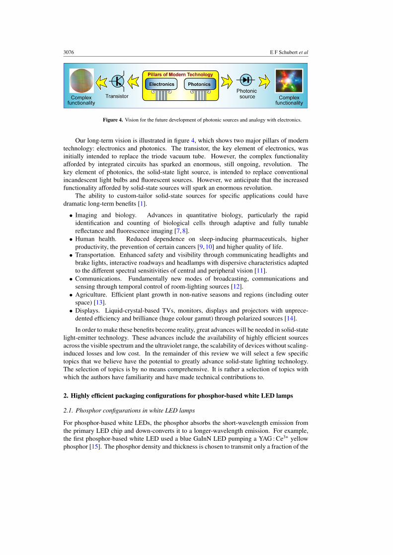
Figure 4. Vision for the future development of photonic sources and analogy with electronics.
Our long-term vision is illustrated in figure 4, which shows two major pillars of moderntechnology: electronics and photonics. The transistor, the key element of electronics, wasinitially intended to replace the triode vacuum tube. However, the complex functionalityafforded by integrated circuits has sparked an enormous, still ongoing, revolution. Thekey element of photonics, the solid-state light source, is intended to replace conventionalincandescent light bulbs and fluorescent sources. However, we anticipate that the increasedfunctionality afforded by solid-state sources will spark an enormous revolution.
The ability to custom-tailor solid-state sources for specific applications could havedramatic long-term benefits [1].
• Imaging and biology. Advances in quantitative biology, particularly the rapididentification and counting of biological cells through adaptive and fully tunablereflectance and fluorescence imaging [7, 8].
• Human health. Reduced dependence on sleep-inducing pharmaceuticals, higherproductivity, the prevention of certain cancers [9, 10] and higher quality of life.
• Transportation. Enhanced safety and visibility through communicating headlights andbrake lights, interactive roadways and headlamps with dispersive characteristics adaptedto the different spectral sensitivities of central and peripheral vision [11].
• Communications. Fundamentally new modes of broadcasting, communications andsensing through temporal control of room-lighting sources [12].
• Agriculture. Efficient plant growth in non-native seasons and regions (including outerspace) [13].
• Displays. Liquid-crystal-based TVs, monitors, displays and projectors with unprece-dented efficiency and brilliance (huge colour gamut) through polarized sources [14].
In order to make these benefits become reality, great advances will be needed in solid-statelight-emitter technology. These advances include the availability of highly efficient sourcesacross the visible spectrum and the ultraviolet range, the scalability of devices without scaling-induced losses and low cost. In the remainder of this review we will select a few specifictopics that we believe have the potential to greatly advance solid-state lighting technology.The selection of topics is by no means comprehensive. It is rather a selection of topics withwhich the authors have familiarity and have made technical contributions to.
2. Highly efficient packaging configurations for phosphor-based white LED lamps
2.1. Phosphor configurations in white LED lamps
For phosphor-based white LEDs, the phosphor absorbs the short-wavelength emission fromthe primary LED chip and down-converts it to a longer-wavelength emission. For example,the first phosphor-based white LED used a blue GaInN LED pumping a YAG : Ce3+ yellowphosphor [15]. The phosphor density and thickness is chosen to transmit only a fraction of the

Solid-state lighting—a benevolent technology 3077
Figure 5. Phosphor placements in LED lamps. (a) Proximate phosphor-in-cup distribution [16].(b) Proximate conformal phosphor distribution [16]. (c) Remote phosphor distribution [17, 18].
blue light. Mixing yellow phosphorescence with the blue electroluminescence results in whitelight. The amount, density and distribution of phosphor inside LED packages are adjusted tooptimize the colour-rendering characteristics and the device efficiency.
The placement and arrangement of phosphors are critical for both the luminous sourceefficiency and colour rendering index of the white LED lamps. Typical arrangements ofphosphor in white LED lamps are shown in figure 5. The first generation white LEDs arefabricated by dispensing the phosphor into epoxy within a reflector cup. We refer to thisconfiguration as proximate phosphor-in-cup distribution, as shown in figure 5(a). For thisprocess, it is difficult to control the uniformity of the phosphor distribution and the phosphorgrain size variation, which, for non-uniform distributions, will result in colour variationfor different view angles. Figure 5(b) shows another proximate phosphor distribution, inwhich the phosphor layer conformally coats the LED chip. In this case, the colour variationat different viewing angles is reduced dramatically due to the thickness uniformity of thephosphor layer, which provides the blue emission with an equal optical path length in thephosphor material, independent of the emission direction [16]. For both phosphor-in-cup andconformal phosphor distributions, phosphors are closely distributed around the LED chip.Because the phosphorescence emission is isotropic, a large portion of the light emitted fromphosphor directly impinges on the LED chip. The contacts and bonding metals of the LEDchip are absorptive at the phosphorescence wavelength [19]. This issue is especially severein conformal phosphor distribution due to the close proximity between the phosphor and theabsorptive LED chip.
Placing the phosphor layer at a sufficiently large distance from the LED chip, as shownin figure 5(c), reduces the probability of the phosphorescence directly hitting the chip. Thephosphor forms a uniform layer on the top of the reflector cup, which we refer to as remotephosphor [17,18]. The thickness of the remote phosphor can be well controlled, which resultsin excellent colour uniformity. In addition, the separation of phosphor from the LED chipreduces the operating temperature for phosphor, which in turn is expected to improve the lamplifetime.
2.2. Whispering-gallery modes and diffuse reflector cups
Most of the metal reflector cups employed in LED packages have a truncated-cone shapefor reflecting the LED emission towards the top and out of the package. For white LED
3078 E F Schubert et al
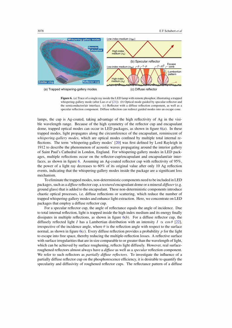
Figure 6. (a) Trace of a single ray inside the LED lamp with remote phosphor, illustrating a trappedwhispering-gallery mode (after Luo et al [21]). (b) Optical mode guided by specular reflector andthe semiconductor/air interface. (c) Reflector with a diffuse reflection component, as well as aspecular reflection component. Diffuse reflection can redirect guided modes into an escape cone.
lamps, the cup is Ag-coated, taking advantage of the high reflectivity of Ag in the visi-ble wavelength range. Because of the high symmetry of the reflector cup and encapsulantdome, trapped optical modes can occur in LED packages, as shown in figure 6(a). In thesetrapped modes, light propagates along the circumference of the encapsulant, reminiscent ofwhispering-gallery modes, which are optical modes confined by multiple total internal re-flections. The term ‘whispering-gallery modes’ [20] was first defined by Lord Rayleigh in1912 to describe the phenomenon of acoustic waves propagating around the interior galleryof Saint Paul’s Cathedral in London, England. For whispering-gallery modes in LED pack-ages, multiple reflections occur on the reflector-cup/encapsulant and encapsulant/air inter-faces, as shown in figure 6. Assuming an Ag-coated reflector cup with reflectivity of 95%,the power of a light ray decreases to 60% of its original value after only 10 Ag reflectionevents, indicating that the whispering-gallery modes inside the package are a significant lossmechanism.
To eliminate the trapped modes, non-deterministic components need to be included in LEDpackages, such as a diffuse reflector cup, a textured encapsulant dome or a mineral diffuser (e.g.ground glass) that is added to the encapsulant. These non-deterministic components introducechaotic optical processes, i.e. diffuse reflections or scattering, which reduce the number oftrapped whispering-gallery modes and enhance light extraction. Here, we concentrate on LEDpackages that employ a diffuse reflector cup.
For a specular reflector cup, the angle of reflectance equals the angle of incidence. Dueto total internal reflection, light is trapped inside the high index medium and its energy finallydissipates in multiple reflections, as shown in figure 6(b). For a diffuse reflector cup, thediffusely reflected light I has a Lambertian distribution with an intensity I ∝ cos θ [22],irrespective of the incidence angle, where θ is the reflection angle with respect to the surfacenormal, as shown in figure 6(c). Every diffuse reflection provides a probability p for the lightto escape into free space, thereby reducing the multiple-reflection losses. A reflective surfacewith surface irregularities that are in size comparable to or greater than the wavelength of light,which can be achieved by surface roughening, reflects light diffusely. However, real surface-roughened reflectors almost always have a diffuse as well as a specular reflection component.We refer to such reflectors as partially diffuse reflectors. To investigate the influence of apartially diffuse reflector cup on the phosphorescence efficiency, it is desirable to quantify thespecularity and diffusivity of roughened reflector cups. The reflectance pattern of a diffuse

Solid-state lighting—a benevolent technology 3079
Figure 7. Measured angular dependence of reflectivity for a specular (i.e. smooth) and a diffuse(i.e. roughened by bead blasting) Ag reflector. Fitting the experimental data to the theoretical modelgives a diffuse-to-total-reflected-power ratio of 0.83% and 86% for the specular and diffuse Agreflectors, respectively. Also shown are photos of the two Ag reflector cups.
reflector can be described by [23]:
I (θ, φ) = Idiff cos(θ) + Ispec cos(θ)1
σ 22πexp
[−1
2
(θ − θi
σ
)2]
exp
[−1
2
(φ − φi
σ
)2]
,
(4)
whereφ and θ are the azimuthal and polar angle of reflectance andφi and θi are the azimuthal andpolar angle of incidence, respectively. Idiff is the maximum intensity for diffuse reflection, andIspec cos(θi)1/(σ 22π) is the maximum intensity for specular reflection. The diffuse reflectionintensity, given by the first summand on the right-hand side of equation (4), follows theLambertian distribution. The second summand describes the specular reflection intensity,which is assumed to be broadened as a Gaussian function. Fitting equation (4) to measuredangular dependent reflectivity data of a partially diffuse reflector will give us Idiff , Ispec and σ .The diffuse and specular reflection power (Pdiff and Pspec) are then obtained by integratingthe first and second summand of the equation over space, i.e. over 0◦ � θ � 90◦ and0◦ � φ � 180◦. The diffusivity and specularity are then determined by the equations
diffusivity = Pdiff/(Pdiff + Pspec), (5)
specularity = Pspec/(Pdiff + Pspec). (6)
To investigate the angular dependent reflectivity of specular and diffuse reflector cups, a smoothand a bead-blasted Ag reflector are fabricated and measured using a He–Ne laser emitting at632 nm. The incident angle is 40◦ and the reflected light intensity is measured from −90◦ to90◦, as shown in the inset of figure 7. Compared with the specular reflector, the diffuse reflectorshows a two orders of magnitude higher diffusely reflected power. Fitting equation (4) to theexperimental data gives a diffusivity of 86% for the bead-blasted Ag reflector and of 0.83%for the specular Ag reflector. Photos of Ag coated specular and diffuse reflector cups are alsoshown in figure 7.
3080 E F Schubert et al
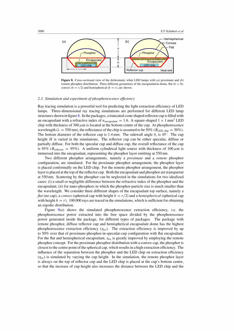
Figure 8. Cross-sectional view of the dichromatic white LED lamps with (a) proximate and (b)remote phosphor distribution. Three different geometries of the encapsulation dome, flat (h = 0),convex (h = r/2) and hemispherical (h = r), are shown.
2.3. Simulation and experiment of phosphorescence efficiency
Ray tracing simulation is a powerful tool for predicting the light extraction efficiency of LEDlamps. Three-dimensional ray tracing simulations are performed for different LED lampstructures shown in figure 8. In the packages, a truncated-cone shaped reflector cup is filled withan encapsulant with a refractive index of nencapsulant = 1.6. A square-shaped 1 × 1 mm2 LEDchip with thickness of 300 µm is located at the bottom centre of the cup. At phosphorescencewavelength (λ = 550 nm), the reflectance of the chip is assumed to be 50% (RLED chip = 50%).The bottom diameter of the reflector cup is 1.4 mm. The sidewall angle θs is 45◦. The cupheight H is varied in the simulations. The reflector cup can be either specular, diffuse orpartially diffuse. For both the specular cup and diffuse cup, the overall reflectance of the cupis 95% (Rreflector = 95%). A uniform cylindrical light source with thickness of 100 µm isimmersed into the encapsulant, representing the phosphor layer emitting at 550 nm.
Two different phosphor arrangements, namely a proximate and a remote phosphorconfiguration, are simulated. For the proximate phosphor arrangement, the phosphor layeris placed conformally on the LED chip. For the remote phosphor arrangement, the phosphorlayer is placed at the top of the reflector cup. Both the encapsulant and phosphor are transparentat 550 nm. Scattering by the phosphor can be neglected in the simulations for two idealizedcases: (i) a small or negligible difference between the refractive index of the phosphor and theencapsulant; (ii) for nano-phosphors in which the phosphor-particle size is much smaller thanthe wavelength. We consider three different shapes of the encapsulant top surface, namely aflat (no cap), a convex (spherical cap with height h = r/2) and a hemispherical (spherical capwith height h = r). 100 000 rays are traced in the simulations, which is sufficient for obtainingan ergodic distribution.
Figure 9(a) shows the simulated phosphorescence extraction efficiency, i.e. thephosphorescence power extracted into the free space divided by the phosphorescencepower generated inside the package, for different types of packages. The package withremote phosphor, diffuse reflector cup and hemispherical encapsulant dome has the highestphosphorescence extraction efficiency (ηex). The extraction efficiency is improved by upto 50% over that of proximate-phosphor-in-specular-cup configuration with flat encapsulant.For the flat and hemispherical encapsulant, ηex is greatly improved by employing the remotephosphor concept. For the proximate phosphor distribution with a convex cap, the phosphor isclosest to the centre point of the spherical cap, which results in a high extraction efficiency. Theinfluence of the separation between the phosphor and the LED chip on extraction efficiency(ηex) is simulated by varying the cup height. In the simulation, the remote phosphor layeris always on the top of reflector cup and the LED chip is placed at the cup’s bottom centre,so that the increase of cup height also increases the distance between the LED chip and the

Solid-state lighting—a benevolent technology 3081
Figure 9. (a) Simulated phosphorescence-extraction efficiency for different types of packages. (b)The phosphorescence extraction efficiency increases with increasing cup height for both specularand diffuse reflector cups.
Figure 10. (a) Percentage of trapped modes (>10 Ag reflections) inside the white LED lamps withremote phosphor for a flat, convex and hemispherical encapsulant shape. Influence of diffusivityof reflector cup on (b) percentage of trapped modes and (c) phosphor extraction efficiency.
phosphor layer. The simulation results, given in figure 9(b), clearly show that ηex is improvedby increasing the separation between the phosphor layer and the LED chip, confirming ourpredictions.
It is apparent from the simulations that the diffuse reflector cup enhances the extractionof phosphorescence. We believe that the enhancement is due to the reduction of whispering-gallery modes by the diffuse reflector cup which randomizes the propagation direction oftrapped optical rays in the packages. The fraction of trapped modes for different encapsulationgeometries and reflector cups are simulated, as shown in figure 10, to demonstrate the existenceof whispering-gallery modes. We define trapped optical modes as modes that incur more than10 reflection events from the Ag reflector cup. For a lamp package with specular reflectorcup, 25%, 32% and 14% of the emission rays are trapped for a flat, convex and hemisphericalencapsulation shape, respectively. By employing a diffuse reflector cup, the fraction of trappedmodes is significantly reduced, irrespective of the encapsulant geometry. 58% and 86% oftrapped modes are extracted out into free space by employing a diffuse reflector cup for convexand hemispherical encapsulation shapes, respectively.
Diffusivity is one of the most important parameters for a roughened reflector, whichdirectly influences the extraction of whispering-gallery modes. According to our simulations,the fraction of trapped modes decreases rapidly with increasing reflector diffusivity, as shown

3082 E F Schubert et al
Figure 11. Emission spectra (——) of a blue-pumped white LED lamp with yellow phosphor anda UV-pumped dichromatic LED lamp with blue phosphor. The dashed lines show the emissionfrom reference LEDs packaged without phosphor. De-convolution of the spectra into emissionfrom the LED chip and emission from the phosphor is shown in the inset.
in figure 10(b). For a reflector cup with a diffusivity of 86%, the percentage of trapped modesdecreases to 4.8%, 14.7% and 2.0% for flat, convex and hemispherical encapsulant shapes,respectively. Accordingly, the phosphorescence extraction efficiency ηex is improved withincreasing diffusivity of the reflector cup, as shown in figure 10(c). There is a slight decreasein efficiency for lamps with a flat encapsulant when the diffusivity of the cup exceeds 60%although the trapped modes are reduced. It is believed that the decrease in efficiency is causedby the Lambertian reflection pattern, which guides a small amount of the light down to theabsorptive LED chip.
Two types of dichromatic LED lamps have been fabricated, one of them comprising aUV GaInN LED (λ = 400 nm) pumping a blue phosphor and the other one comprising a blueGaInN LED (λ = 470 nm) pumping a yellow phosphor. Different phosphor arrangementsand reflector cups are employed. For diffuse reflector cups, the sidewalls are roughened bybead-blasting to achieve diffuse reflection. The LED chips are die-bonded to the bottom of thereflector cups followed by the wire bonding process. For the proximate phosphor configuration,the phosphor is uniformly mixed into an epoxy resin and filled into the reflector cup. For theremote phosphor configuration, the transparent epoxy resin (without phosphor) is filled intothe reflector cup and cured. Then, a layer of phosphor and epoxy mixture is uniformly coatedon the top of the cured epoxy, as shown in figure 5(c). After the phosphor and epoxy mixturelayer is cured, reflector cups containing an LED chip and a phosphor are encapsulated by thestandard LED packaging technology. LEDs without phosphor are packaged as reference lampsthat are used to calculate the phosphor conversion efficiency.
The emission spectra of the reference LED emitters and of the dichromatic lamps operatingat 20 mA, shown in figure 11, are measured using an integrating sphere. As illustrated in theinset, the spectra of dichromatic lamps were de-convoluted into primary LED emission andphosphorescence emission. By integrating the de-convoluted spectra, the optical power ofeach part is obtained. Table 3 shows the phosphor power conversion efficiencies, whichare calculated by dividing the measured optical power from the phosphor by the difference inoptical power between the LED emission of the reference lamp (without phosphor) and primaryLED emission of the dichromatic lamp. For the dichromatic white lamp with the blue LED

Solid-state lighting—a benevolent technology 3083
Table 3. Phosphor power-conversion efficiency of dichromatic LED lamps with different reflectorcup and phosphor configurations. The numbers in the parenthesis show the enhancement ofphosphor power-conversion efficiency compared with that of a specular cup with proximatephosphor configuration. The power conversion efficiency given in the table is the product of thewavelength conversion efficiency, ηw = (hυ1 − hυ2)/hυ1, and the phosphor quantum efficiency.
Phosphor power conversion efficiency (%)
UV LED + blue phosphor Blue LED + yellow phosphor
Specular cup 67.9 59.9Proximate phosphor ( - ) ( - )Specular cup 76.8 64.6Remote phosphor (13.1%) (7.8%)Diffuse cup 86.2 69.4Remote phosphor (27.0%) (15.4%)
pumping the yellow phosphor, the phosphor conversion efficiency is improved by 7.8% forthe remote phosphor with specular cup configuration and by 15.4% for the remote phosphorwith diffuse cup configuration over the proximate-phosphor-in-specular-cup configuration.As for the UV-pumped blue phosphor configuration, the enhancement of power conversionefficiency is even higher due to the low reflectivity of the Ag reflector at short wavelengths.A 27% improvement is obtained for the remote phosphor with diffuse cup configurationcompared with the proximate-phosphor-in-specular-cup configuration. These experimentalresults are fully consistent with the ray tracing simulations, confirming the enhancementof phosphor efficiency by employing a diffuse reflector cup with the remote phosphorconfiguration.
3. Omni-directional reflectors for light-emitting diodes
This section discusses possible solutions to limitations in light-extraction efficiency of light-emitting diodes (LEDs) using new types of triple-layer omni-directional reflectors (ODRs).The ODRs have lower mirror losses than metal reflectors and distributed Bragg reflectors(DBRs). High-reflectivity ODRs have been incorporated into GaInN LEDs and AlGaInPLEDs. It is shown that the ODR significantly increases light extraction from ODR-LEDs ascompared to reference LEDs employing a DBR or a metal reflector.
3.1. Reflectors for light-emitting diodes
One of the fundamental ways to reduce optical losses in light-emitting devices is theemployment of optical reflectors with near-perfect reflection characteristics. For example,a strong optical loss mechanism in GaInN-based flip-chip LED structures is due to thelow reflectivity of the p-type contact such as oxidized Ni/Au. Because multiple reflectionevents can occur in LED structures, mirror losses should be kept at a minimum by usingreflectors with near-perfect reflection characteristics. Such near-perfect characteristicsof a reflector include (i) high reflectivity, (ii) omni-directionality, (iii) broad spectralrange of the high-reflectivity band and (iv) electrical conductivity for current-injectedstructures.
There are several reflectors used in current LED structures including metal reflectors,DBRs and ODRs. The structure and the optical/electrical characteristics of these reflectorsare given in table 4. Metal reflectors are electrically-conducting reflectors capable of

3084 E F Schubert et al
Table 4. Schematic structures and electrical/optical characteristics of metal reflectors, distributedBragg reflectors (DBRs) and triple-layer omni-directional reflectors (ODRs).
Metal Distributed Bragg Triple-layer omni-directionalreflector reflector (DBR) reflector (ODR)
Structure
Reflectivitya <95% ∼99% ∼99%Omni-directionality Yes No YesSpectral width Broad Narrow BroadElectrical conductivity Good — —-
a Reflectivity depends on wavelength and optical properties of reflector materials.
reflecting visible light over a wide range of wavelengths and incident angles, i.e. showingomni-directionality and broad spectral width. However, reflectivity of metal reflectors onsemiconductors is typically at most 95%. For example, Ag, which shows highest reflectivityamong metals at visible wavelengths, exhibits normal-incidence reflectivity on GaN of ∼91%at 470 nm. DBRs are periodic structures with a unit cell of two dielectric layers havingdifferent refractive indices ni and quarter-wavelength thicknesses di (i = 1, 2). DBRscan be considered as one-dimensional photonic crystals that have a high-reflectivity stopband due to the non-propagating light states in the structure. Therefore, one can designa DBR to have a reflectivity as high as ∼99% at a certain centre wavelength for normalincidence. However, the DBR reflectivity depends on the incidence angle θ so that thestop band shifts towards shorter wavelengths for increasing θ without changing its spectralwidth. As a result, DBRs become transparent for oblique angles of incidence. In addition,the reflectivity of DBRs also depends on the polarization of the incident light. According toBrewster’s law, the reflection of light polarized parallel to the plane of incidence (TM mode)has a minimum at the Brewster angle θB = arc tan (n1/n2), where n1 and n2 are therefractive indices of the two adjoining media. Therefore, the overall reflectivity, (TM mode+ TE mode)/2, significantly decreases near θB. Furthermore, the applicability of DBRs in
LEDs is limited due to the electrically insulating and thermally-resistant nature of dielectriclayers.
Recently, a very promising triple-layer ODR suitable for LED technology has beenintroduced. The triple-layer ODR comprises a semiconductor with a refractive index ns, alow-refractive index layer (nli) and a metal with a complex refractive index Nm = nm + ikm,where km is the extinction coefficient. Triple-layer ODRs with high reflectivity, wide stopband and omni-directional reflection characteristics have been demonstrated and have shownthe ability to easily outperform metal reflectors and DBRs [24–26].
The reflectance of a semiconductor/metal reflector as a function of the incident angle θ isgiven by [27]
RTE =∣∣∣∣ns cos θ1 − Nm cos θ2
ns cos θ1 + Nm cos θ2
∣∣∣∣2
and RTM =∣∣∣∣∣
nscos θ1
− Nmcos θ2
nscos θ1
+ Nmcos θ2
∣∣∣∣∣2
. (7)
The reflectance of the triple-layer ODR as a function of the incident angle θ is given by [27]
R =∣∣∣∣ r01 + r12 exp(2iφ)
1 + r01r12 exp(2iφ)
∣∣∣∣2
, (8)

Solid-state lighting—a benevolent technology 3085
Figure 12. Calculated reflectivity for a 35-period (Al0.3Ga0.7)0.5In0.5P/Al0.5In0.5P DBR, a 35period AlAs/GaAs DBR and a triple layer ODR (GaP/SiO2/Ag). GaP was chosen as the externalmedium. (a) Reflectivity versus wavelength for normal incidence and (b) angular dependence ofthe reflectivity at 630 nm (after Gessmann and Schubert [25]).
where
r01TE = ns cos θ1 − nli cos θ2
ns cos θ1 + nli cos θ2, r01TM = nli cos θ1 − ns cos θ2
nli cos θ1 + ns cos θ2,
r12TE = nli cos θ2 − Nm cos θ3
nli cos θ2 + Nm cos θ3, r12TM = Nm cos θ2 − nli cos θ3
Nm cos θ2 + nli cos θ3
and φ = 2π
λnlih cos θ2.
Equation (8) applies to a low-index dielectric layer thickness of λ0/(4nli), i.e. to a quarterwavelength layer. Figure 12 shows calculated reflectivity for an Ag/SiO2/GaP ODR and twoDBRs, an AlGaInP DBR and an AlGaAs DBR, both incorporated in an AlGaInP LED emittingat 630 nm. The AlGaAs DBR consists of 35 periods of AlAs/GaAs and the AlGaInP DBRconsists of 35 periods of (Al0.3Ga0.7)0.5In0.5P/Al0.5In0.5P, designed to have a high normal-incidence reflectivity at the centre wavelength of 630 nm, as shown in figure 12(a). TheAlGaInP DBR shows a narrow high-reflectivity stop band between 600 and 670 nm, whilethe reflectivity of Ag/SiO2/GaP ODR shows high reflectivity for all visible wavelengths.Figure 12(b) compares the angular dependence of reflectivity of an Ag/SiO2/GaP ODR withthe two DBRs. While the ODRs maintain high reflectivity at virtually all angles of incidence,the AlGaInP DBR reflectivity sharply drops above 17◦. Note that the reflectivity of the triple-layer ODR is significantly better at oblique angles of incidence than that of DBRs. It was alsoshown that the angular-averaged reflectivity of the Ag/SiO2/GaN ODR is much higher thanthat of a 20 period Al0.25Ga0.75N/GaN DBR and Ag metal reflector at 470 nm (nAg = 0.132,kAg = 2.72, nSiO2 = 1.46, nGaN = 2.454 at 470 nm) [25]. High reflectivity is essential tominimize the losses of waveguided modes which are common in LEDs. These theoreticalconsiderations show the huge advantages offered by ODRs.
3.2. GaInN blue light-emitting diodes with omni-directional reflectors
Recently, GaN blue LEDs having new types of ODRs with high reflectivity, wide stop band andomni-directional reflection characteristics have been demonstrated [26, 28, 29]. Figure 13(a)shows a typical GaN-based LED structure comprising a mesa with the common ‘p-side-up’

3086 E F Schubert et al
Figure 13. (a) Typical GaInN-based LED structure comprising a mesa with common ‘p-side-up’growth on sapphire substrate. Schematic cross-sectional view of (b) a GaN/ITO/Ag ODR (afterGessmann et al [29]) and (c) a GaN/RuO2/SiO2/Ag ODR. The SiO2 low-refractive-index layer isperforated by micro-contacts enabling electrical conductivity between the RuO2 contact layer andAg (after Kim et al [26]).
growth on a sapphire substrate. The first ODR structure incorporated into a GaN blue LEDis shown in figure 13(b) [29]. The ODR consists of GaN, a transparent and electricallyconductive ITO with quarter-wavelength thickness and a Ag layer, based on high/low/highcomplex refractive index of the Ag (nAg = 0.132, kAg = 2.72 at 470 nm), ITO (nITO = 2.06at 470 nm) and GaN (nGaN = 2.45 at 470 nm). The GaN LED structure was grown by organo-metallic vapour-phase epitaxy (OMVPE) and consists of a thick n-type GaN buffer layer, ann-type GaN lower cladding layer, a GaInN/GaN multiple quantum well active region, a p-typeGaN upper cladding and a highly doped contact layer. LED mesa structures were fabricated bystandard photolithographic patterning followed by dry-etching to expose the n-type claddinglayer. After a 3 min dip in buffered oxide etchant (BOE), p-type contacts for the ODR-LEDswere deposited in a two-step process: first, an ITO film of quarter wavelength thickness wasdeposited by RF-assisted sputtering. The ITO was then annealed in a rapid thermal annealing(RTA) furnace at 600 ◦C under an N2 atmosphere for 30 s. The ITO film was virtually colourlessand transparent. In the second step, Ag (200 nm) and Au (20 nm) were deposited on top of theannealed ITO layer by electron-beam evaporation. For comparison, LEDs with conventionalNi/Au contacts were fabricated on the same wafer. The n-type contacts for both samples werefabricated by electron-beam evaporation of Ti/Al (60/60 nm) contacts without oxide removal orsubsequent annealing. It was shown that the ODR-LEDs have lower optical losses and higherextraction efficiency as compared with conventional LEDs with Ni/Au contacts. However,the ODR-LED showed a high forward voltage, possibly due to a high contact resistivity ofITO/p-GaN.
An ODR structure that includes a RuO2 current-spreading layer has been incorporatedinto a GaInN blue LED as shown in figure 13(c) [26]. The ODR comprises GaN, a thinlayer of oxidized ruthenium (Ru) used as semitransparent low-resistance p-type ohmic contacta quarter-wave thick SiO2 low-refractive index layer perforated by an array of Ag micro-contacts, and a thick Ag layer. The GaInN LED structure was grown by OMVPE on c-planesapphire substrate. After a dry-etching for LED mesa structure, Ru (5.0 nm) was deposited onp-type GaN and annealed at 500 ◦C in an O2 atmosphere to form RuO2 which acts as an ohmiccontact to p-type GaN. The RuO2 obtained by this oxidation annealing was virtually colourlessand transparent. A quarter-wave thick SiO2 layer was deposited on the RuO2 using plasma-enhanced chemical vapour deposition (PECVD). Then, an array of circular micro-contacts wasetched into the SiO2, by using BOE, to expose the conducting RuO2 layer. Ag (200 nm) andAu (20 nm) were deposited by electron-beam evaporation on top of the SiO2 patterned withmicro-contact holes. For comparison, LEDs with conventional Ni/Au and Ag contacts werefabricated on the same wafer. The n-type contacts formed readily by electron-beam depositionof Ti/Al/Ni/Au (30/120/40/50 nm). No oxide removal or subsequent annealing was neededfor contact formation.

Solid-state lighting—a benevolent technology 3087
Figure 14. (a) Top view of the GaInN LED with GaN/RuO2/SiO2/Ag ODR. The SiO2lowrefractive- index layer is perforated by micro-contacts enabling electrical conductivity betweenthe RuO2 contact layer and Ag. (b) Current–voltage characteristics and (c) light-output-versus-current characteristic of GaInN LED with GaN/RuO2/SiO2/Ag ODRs and LEDs with Ni/Au andAg contacts (after Kim et al [26]).
Figure 14(a) shows a top view of the GaInN LED with GaN/RuO2/SiO2/Ag ODR. Thechip dimensions are 300 × 300 µm2. There is an array of circular micro-contacts in thep-contact area, enabling electrical conductivity between the RuO2 contact layer and Agthrough the insulating SiO2 low-index layer. The diameter of the micro-contacts is 4 µm.Figure 14(b) shows I–V characteristics of the LED with GaN/RuO2/SiO2/Ag ODR and theconventional LEDs with Ni/Au and Ag contacts. The forward voltage at 20 mA for the LEDwith GaN/RuO2/SiO2/Ag ODR is 4.0 V, comparable to that of the conventional LED withNi/Au contact, 3.9 V. This indicates that the contact resistivity of RuO2 on p-type GaN iscomparable to that of Ni/Au. Because the RuO2 contact layer, one of the conducting metaloxides, has a low resistivity (∼50 µ� cm) and a high work function (>5 eV), the material actsas an excellent current spreading and low-resistance contact layer to p-type GaN. On the otherhand, the forward voltage of the LED with a Ag contact is as high as 6.5 V. This is due to alow work function of Ag (4.26 eV), resulting in a high potential barrier between Ag and p-typeGaN.
The electroluminescence intensity from the backsides of the LEDs was measured directlyon a large-size (10 × 10 mm2) Si PIN photodetector. The light-output-versus-currentcharacteristic of the LEDs is shown in figure 14(c). At small forward currents (I < 20 mA),the light power extracted from the LED with ODR is slightly larger than the output fromthe LED with an Ag contact, but significantly larger than that from the LED with a Ni/Aucontact. The increased light output of the LED with ODR can be attributed to a higherreflectivity and hence better light-extraction efficiency due to the use of the ODR. In addition,saturation of the light output power with increasing current level is not observed for the LEDwith GaN/RuO2/SiO2/Ag ODR, indicating that the resistivity of the RuO2 layer and specificcontact resistance of the GaN/RuO2 contact is sufficiently low for LED applications.
Oblique-angle deposition is a method to grow highly porous thin films consisting of anarray of nano-rods. The nano-rod growth is caused by the self-shadowing nature of the oblique-angle deposition process. This process will be described in detail in the next section. Severalnano-rod ITO films, grown by oblique-angle electron-beam deposition on Si substrates witha vapour flux incident angle θ of 80◦, are found to be optically transparent and electricallyconductive. Pure ITO granules are used as evaporation source, and the deposition rate is wellcontrolled at 0.5 nm s−1. Figure 15(a) shows the cross-sectional scanning electron micrograph(SEM) of the nano-rod ITO layer. The nano-rod ITO is uniformly distributed with a tilt angle

3088 E F Schubert et al
Figure 15. (a) Cross-sectional scanning electron micrograph (SEM) of the ITO nano-rod layeron Si substrate. Inset shows the top view of the ITO nano-rod layer. Atomic force micrographsof the surface of (b) dense ITO layer and (c) ITO nano-rod layer with pore-closure ITO layer. (d)Refractive index of dense ITO and low-n ITO films versus wavelength measured using ellipsometry.
of θt = 45◦. The gap between the nano-rod ITO is less than 50 nm, i.e. much smaller thanthe wavelength of visible light, thereby limiting optical scattering. The nano-rod ITO thinfilm obtained by the oblique-angle deposition is specular, featureless and virtually colourlessand transparent. Furthermore, since the film is deposited by evaporation, the controllabilityof film thickness is excellent, very suitable for quarter-wavelength thickness optical films.Therefore, oblique-angle deposition is promising for the growth of optical coatings with verylow-refractive index, which are advantageous for ODRs with high-refractive-index contrast.The inset in figure 15(a) shows the SEM top view of the nano-rod ITO film including openingsbetween the nano-rods. In order to avoid the filling of subsequent metal into these openings,a surface-sealing step is employed by depositing an ITO pore-closure layer. The atomic-forcemicrographs (AFM) of the surface of the dense ITO layer and the nano-rod ITO layer withpore-closure layer are shown in figures 15(b) and (c), respectively. The root-mean-square(rms) surface roughness of the dense ITO layer, which is electron-beam deposited with normalincidence of the vapour flux, is 4.2 nm. The rms roughness of the nano-rod ITO layer withoutpore-closure layer is 8.3 nm, higher than that of the dense ITO layer, due to the openingsbetween the nano-rods. After the pore-closure layer deposition, the rms roughness reduces to4.2 nm, and there is no indication of openings between the nano-rods, as shown in figure 15(c).
The refractive index of the nano-rod ITO films is measured with ellipsometry using theincident angles 60◦, 65◦ and 70◦. A ‘Cauchy layer on Si substrate’ is used as the ellipsometrymodel and found to fit the measurement data very well. The refractive index of the nano-rodITO films versus wavelength is shown in figure 15(d). Over the entire visible spectrum, therefractive index of the nano-rod ITO layer is n < 1.35. At 461 nm, the refractive index of thenano-rod ITO layer is n = 1.34, much lower than the refractive index of dense ITO, n = 2.06,and even lower than that of SiO2, n = 1.46.
The low-n ITO is incorporated into a GaInN LED emitting at a peak wavelength of474 nm. The GaInN LED structure was grown by OMVPE on c-plane sapphire substrateand consists of a 3 µm thick n-type GaN buffer layer, an n-type GaN lower cladding layer, aGaInN/GaN multiple quantum well active region, a p-type GaN upper cladding and a highlydoped p-type GaN contact layer. A quarter-wavelength-thick low-n ITO layer was depositedby oblique-angle electron-beam deposition with an incident angle of 80◦. After the low-nITO deposition, a very thin (20 nm) pore-closure layer is formed on top of the low-n ITOlayer with an incident angle of −45◦. After the pore-closure layer, a 200 nm-thick Ag layeris deposited by electron-beam evaporation. LED mesa structures were obtained by standardphotolithographic patterning followed by chemically-assisted ion-beam etching using Cl2 andAr to expose the n-type cladding layer. For comparison, LEDs with an Ag reflector werefabricated on the same wafer piece.
Solid-state lighting—a benevolent technology 3089
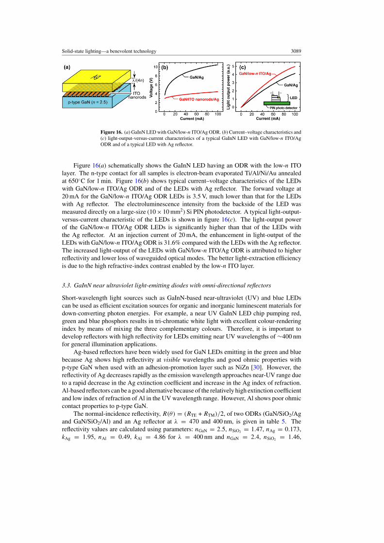
Figure 16. (a) GaInN LED with GaN/low-n ITO/Ag ODR. (b) Current–voltage characteristics and(c) light-output-versus-current characteristics of a typical GaInN LED with GaN/low-n ITO/AgODR and of a typical LED with Ag reflector.
Figure 16(a) schematically shows the GaInN LED having an ODR with the low-n ITOlayer. The n-type contact for all samples is electron-beam evaporated Ti/Al/Ni/Au annealedat 650◦C for 1 min. Figure 16(b) shows typical current–voltage characteristics of the LEDswith GaN/low-n ITO/Ag ODR and of the LEDs with Ag reflector. The forward voltage at20 mA for the GaN/low-n ITO/Ag ODR LEDs is 3.5 V, much lower than that for the LEDswith Ag reflector. The electroluminescence intensity from the backside of the LED wasmeasured directly on a large-size (10 × 10 mm2) Si PIN photodetector. A typical light-output-versus-current characteristic of the LEDs is shown in figure 16(c). The light-output powerof the GaN/low-n ITO/Ag ODR LEDs is significantly higher than that of the LEDs withthe Ag reflector. At an injection current of 20 mA, the enhancement in light-output of theLEDs with GaN/low-n ITO/Ag ODR is 31.6% compared with the LEDs with the Ag reflector.The increased light-output of the LEDs with GaN/low-n ITO/Ag ODR is attributed to higherreflectivity and lower loss of waveguided optical modes. The better light-extraction efficiencyis due to the high refractive-index contrast enabled by the low-n ITO layer.
3.3. GaInN near ultraviolet light-emitting diodes with omni-directional reflectors
Short-wavelength light sources such as GaInN-based near-ultraviolet (UV) and blue LEDscan be used as efficient excitation sources for organic and inorganic luminescent materials fordown-converting photon energies. For example, a near UV GaInN LED chip pumping red,green and blue phosphors results in tri-chromatic white light with excellent colour-renderingindex by means of mixing the three complementary colours. Therefore, it is important todevelop reflectors with high reflectivity for LEDs emitting near UV wavelengths of ∼400 nmfor general illumination applications.
Ag-based reflectors have been widely used for GaN LEDs emitting in the green and bluebecause Ag shows high reflectivity at visible wavelengths and good ohmic properties withp-type GaN when used with an adhesion-promotion layer such as NiZn [30]. However, thereflectivity of Ag decreases rapidly as the emission wavelength approaches near-UV range dueto a rapid decrease in the Ag extinction coefficient and increase in the Ag index of refraction.Al-based reflectors can be a good alternative because of the relatively high extinction coefficientand low index of refraction of Al in the UV wavelength range. However, Al shows poor ohmiccontact properties to p-type GaN.
The normal-incidence reflectivity, R(θ) = (RTE + RTM)/2, of two ODRs (GaN/SiO2/Agand GaN/SiO2/Al) and an Ag reflector at λ = 470 and 400 nm, is given in table 5. Thereflectivity values are calculated using parameters: nGaN = 2.5, nSiO2 = 1.47, nAg = 0.173,kAg = 1.95, nAl = 0.49, kAl = 4.86 for λ = 400 nm and nGaN = 2.4, nSiO2 = 1.46,

3090 E F Schubert et al
Table 5. Normal-incidence reflectivity R(θ) = (RTE + RTM)/2 of two ODRs (GaN/SiO2/Ag andGaN/SiO2/Al) and a Ag reflector on GaN at λ = 400 and 470 nm.
Ag SiO2/Ag ODR SiO2/Al ODR
Normal-incidence reflectivity 0.906 0.942 0.929(λ = 470 nm)
Normal-incidence reflectivity 0.842 0.877 0.933(λ = 400 nm)
Figure 17. Schematic cross-sectional view of GaInN LED with (a) GaN/SiO2/Ag ODR and (b)GaN/SiO2/Al ODR. (c) Light output and forward voltage at 20 mA of the LEDs for differentreflector structures: Ag reflector, GaN/SiO2/Ag ODR and GaN/SiO2/Al ODR.
nAg = 0.135, kAg = 2.7, nAl = 0.68, kAl = 5.6 for λ = 470 nm. The table clearly showsthat the normal-incidence reflectivity is enhanced for the GaN/SiO2/Al ODR compared withboth the GaN/SiO2/Ag ODR and the Ag reflector. In addition to the normal-incidence results,the angle-dependent reflectivity is also enhanced for the GaN/SiO2/Al ODR compared with theGaN/SiO2/Ag ODR and the Ag reflector. This is attributed to the higher reflectivity of triple-layer ODRs compared with metal reflectors and due to the higher extinction coefficient of Al(kAl = 4.86) than that of Ag (kAg = 1.95) at λ = 400 nm.
GaN LEDs emitting at λ = 400 nm with GaN/SiO2/Al ODR, GaN/SiO2/Ag ODR andAg reflector were fabricated in order to experimentally demonstrate the viability of Al-basedODRs. LED mesa structures were obtained by standard photolithographic patterning followedby chemically-assisted ion beam etching using Cl2 and Ar to expose the n-type cladding layer.A thin NiZn (10 wt% of Zn) was deposited on p-type GaN by electron-beam evaporationfollowed by the deposition of quarter-wavelength-thick SiO2 using PECVD. Then, an array ofmicro-contacts was patterned on SiO2 and etched using BOE to expose the p-type GaN layer.Because of the poor ohmic property of Al on p-type GaN, Ag (60 nm) is deposited on micro-contact holes by electron-beam evaporation and lift off in a self-aligned process, followedby annealing in O2 atmosphere to form a low-resistance ohmic contact. Then, the Al layerwas deposited by electron-beam evaporation on the entire p-type GaN area. For comparison,LEDs with NiZn/Ag (2/60 nm) contacts and LEDs with GaN/SiO2/Ag ODR were fabricatedon different pieces of the same wafer. The n-type contacts for the samples were fabricatedby electron-beam evaporation of Ti/Al/Ni/Au. Figures 17(a) and (b) show schematic cross-sectional views of a GaInN LED with GaN/SiO2/Ag ODR, and with GaN/SiO2/Al ODR,respectively.
Figure 17(c) shows light output and forward voltage at 20 mA of the LEDs with an Agreflector, a GaN/SiO2/Ag ODR and a GaN/SiO2/Al ODR. The forward voltage at 20 mAfor the GaN/SiO2/Ag ODR LEDs is 3.37 V, almost the same as that for the LEDs withNiZn/Ag reflector, 3.32 V. This is attributed to the fact that the oxidized NiZn layer could
Solid-state lighting—a benevolent technology 3091
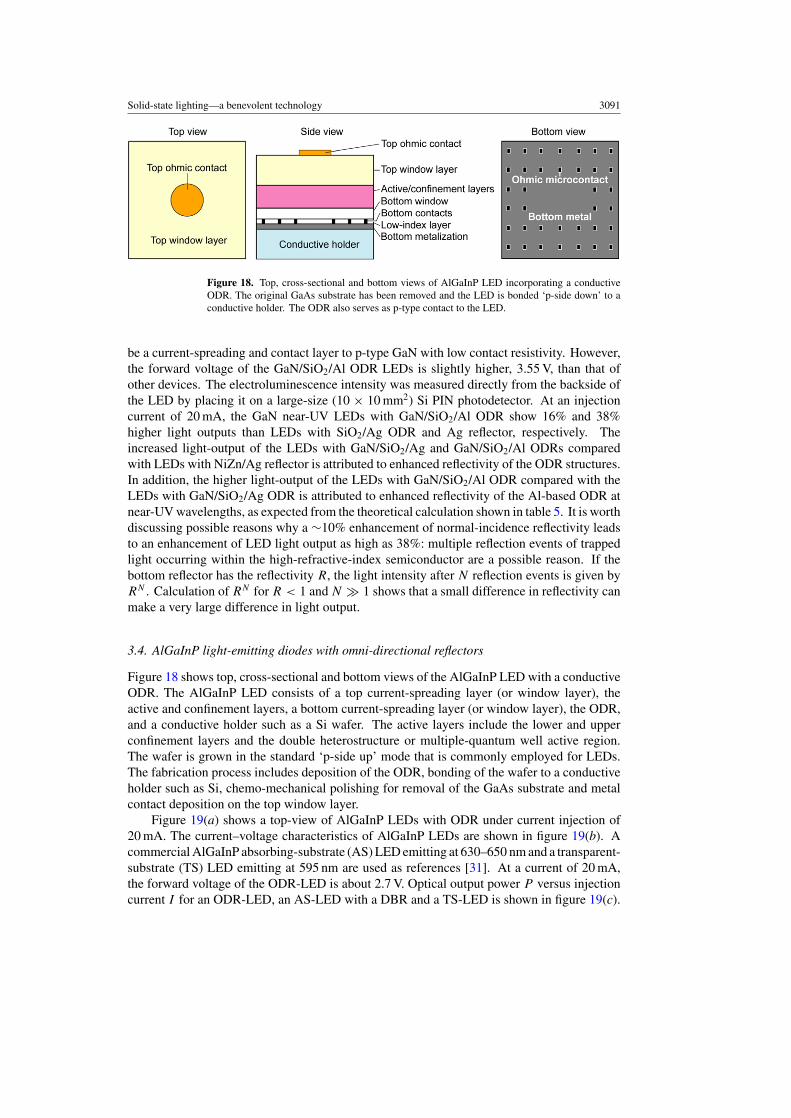
Figure 18. Top, cross-sectional and bottom views of AlGaInP LED incorporating a conductiveODR. The original GaAs substrate has been removed and the LED is bonded ‘p-side down’ to aconductive holder. The ODR also serves as p-type contact to the LED.
be a current-spreading and contact layer to p-type GaN with low contact resistivity. However,the forward voltage of the GaN/SiO2/Al ODR LEDs is slightly higher, 3.55 V, than that ofother devices. The electroluminescence intensity was measured directly from the backside ofthe LED by placing it on a large-size (10 × 10 mm2) Si PIN photodetector. At an injectioncurrent of 20 mA, the GaN near-UV LEDs with GaN/SiO2/Al ODR show 16% and 38%higher light outputs than LEDs with SiO2/Ag ODR and Ag reflector, respectively. Theincreased light-output of the LEDs with GaN/SiO2/Ag and GaN/SiO2/Al ODRs comparedwith LEDs with NiZn/Ag reflector is attributed to enhanced reflectivity of the ODR structures.In addition, the higher light-output of the LEDs with GaN/SiO2/Al ODR compared with theLEDs with GaN/SiO2/Ag ODR is attributed to enhanced reflectivity of the Al-based ODR atnear-UV wavelengths, as expected from the theoretical calculation shown in table 5. It is worthdiscussing possible reasons why a ∼10% enhancement of normal-incidence reflectivity leadsto an enhancement of LED light output as high as 38%: multiple reflection events of trappedlight occurring within the high-refractive-index semiconductor are a possible reason. If thebottom reflector has the reflectivity R, the light intensity after N reflection events is given byRN . Calculation of RN for R < 1 and N � 1 shows that a small difference in reflectivity canmake a very large difference in light output.
3.4. AlGaInP light-emitting diodes with omni-directional reflectors
Figure 18 shows top, cross-sectional and bottom views of the AlGaInP LED with a conductiveODR. The AlGaInP LED consists of a top current-spreading layer (or window layer), theactive and confinement layers, a bottom current-spreading layer (or window layer), the ODR,and a conductive holder such as a Si wafer. The active layers include the lower and upperconfinement layers and the double heterostructure or multiple-quantum well active region.The wafer is grown in the standard ‘p-side up’ mode that is commonly employed for LEDs.The fabrication process includes deposition of the ODR, bonding of the wafer to a conductiveholder such as Si, chemo-mechanical polishing for removal of the GaAs substrate and metalcontact deposition on the top window layer.
Figure 19(a) shows a top-view of AlGaInP LEDs with ODR under current injection of20 mA. The current–voltage characteristics of AlGaInP LEDs are shown in figure 19(b). Acommercial AlGaInP absorbing-substrate (AS) LED emitting at 630–650 nm and a transparent-substrate (TS) LED emitting at 595 nm are used as references [31]. At a current of 20 mA,the forward voltage of the ODR-LED is about 2.7 V. Optical output power P versus injectioncurrent I for an ODR-LED, an AS-LED with a DBR and a TS-LED is shown in figure 19(c).

3092 E F Schubert et al
Figure 19. (a) Top-view micrograph of AlGaInP LED with ODR under current injection of 20 mA.(b) Current-versus-voltage characteristics and (c) dependence of the total optical output power ondrive current for ODR-, DBR- and TS-AlGaInP LEDs emitting at 650 nm, 630 nm and 595 nm,respectively.
The peak wavelengths of the three devices are 650 nm (ODR-LED), 630 nm (DBR-LED) and595 nm (TS-LED) with junction areas Aj ≈ 0.09 mm2, 0.25 mm2 and 0.05 mm2, respectively.In order to measure the total optical output power the samples were placed on a reflectingholder inside an integrating sphere. The largest light output is attained by the ODR-LED.Maximum values of the external quantum efficiencies ηext are about 18% for the ODR-LED(If = 27 mA) and 11% for the DBR-LED (If = 11 mA). TS-LEDs operating at 632 nm have anexternal quantum efficiency of 32% [32]. The external quantum efficiency of the ODR deviceis expected to further increase with a thicker top window layer. The window layer thicknessof the ODR device shown in figure 19 is 2 µm and it is reasonable to expect an improvementby a factor of 2 for ODR devices with a thicker window layer.
4. Low-refractive-index optical thin films and their applications
4.1. Low-refractive-index materials
In distributed Bragg reflectors [33], the refractive index contrast, which is the difference inrefractive index between the two constituting materials, is directly related to the reflectivity,spectral width of stop band and penetration depth. In optical micro-resonators [34], the effectivecavity length and hence the enhancement of spontaneous emission directly depend on the indexcontrast. In photonic crystals [35], the photonic bandgap width is directly related to theindex contrast. This motivates the development of novel optical materials with a refractiveindex much lower than that of any conventional thin-film material. We refer to this new classof materials as ‘low-refractive-index materials’ or ‘low-n materials’.
In semiconductor optoelectronics, the optical ambient material of a reflector frequentlyis a semiconductor, which is a high-refractive-index material with typical refractive index of2.5–3.5. Note that optical reflection characteristics in this case are quite different from thecase where air (n = 1.0) is the optical ambient material. Furthermore, optical reflectors forsemiconductor optoelectronic devices require materials with a very low refractive index. Forexample, in the omni-directional reflector designs for semiconductor optoelectronic devices,the low-n material is a key part as demonstrated by Xi et al [36, 37].
Although multilayer structures with air-gaps have been demonstrated [33], the fabricationprocess requires under-etching and hence is slow and costly. Moreover, air gaps completely

Solid-state lighting—a benevolent technology 3093
Figure 20. Mechanism of porous thin-film growth using oblique-angle deposition and scanning-electron micrographs of SiO2 nano-rod thin film.
lack structural stability, making them unsuitable for most applications. MgF2, CaF2 and SiO2
are materials with refractive indices among the lowest available for conventional, dense opticalcoatings. However, their refractive indices, nMgF2
= 1.39, nCaF2 = 1.44, nSiO2 = 1.46, aremuch higher than the refractive index of air, 1.0. Nano-porous dielectric materials have a lowerrefractive index than dense materials and such nano-porous materials are a promising directionfor the development of low-n materials. We point out that the low-n materials discussed herehave distinctly different requirements than the low-k materials used in Si microelectronicstechnology. In contrast to low-k materials, low-n materials require that Mie and Rayleighscattering, which is irrelevant to low-k materials, be minimized.
Several low-n materials are currently being developed. Nano-porous SiO2 thin filmsfabricated from a sol-gel process [38–40] have a very low refractive index, good mechanicalstrength and low scattering coefficients. Its refractive index can be as low as 1.10 [37, 39].Nano-porous SiO2 fabricated from a sol–gel process has an average pore size 4 nm [41]. Opticalscattering from such nano-structure pores is indeed expected to be very small. However, it maybe difficult to precisely control the thickness and the uniformity of spin-on sol–gel materials.
Teflon AF has a refractive index of 1.32 and is transparent in the visible spectrum. TeflonAF has the lowest refractive index among available organic polymer materials. However,its refractive index is not sufficiently low and, since it requires a spin coating process fordeposition, its film thickness may be difficult to control. Thus, to obtain viable low-n materials,new materials and fabrication methods are needed.
4.2. Oblique-angle deposition for films consisting of an array of nano-rods
Oblique-angle deposition was introduced in the 1950s [42]. It is a technology to grow porous,sculptured thin films [43, 44] enabled by the self-shadowing effect and surface-diffusioneffect [45] during the deposition process [46,47]. Since the films resulting from oblique-angledeposition can have very high porosity, it can be used to fabricate low-n thin film materials.Figure 20 shows the deposition mechanism of oblique-angle deposition. A random growthfluctuation on the substrate produces a shadow region that the subsequent incident vapour fluxcannot reach. Also produced are ‘hills’ where the incident flux deposits preferentially, therebycreating an array of oriented rods with tilt angle of θt . In oblique-angle deposition, the poresize of the porous thin film is determined, among other factors, by random growth fluctuations.This results in average pore sizes, i.e. separations between nano-rods, which are very small.In order to grow highly porous thin films, the incidence angle of the vapour flux with respectto the substrate normal, θ , must be large, preferentially close to 90◦ (grazing angle) [44]. Tohave a uniform and random distribution of nano-rods, the substrate’s initial surface should besmooth.
3094 E F Schubert et al
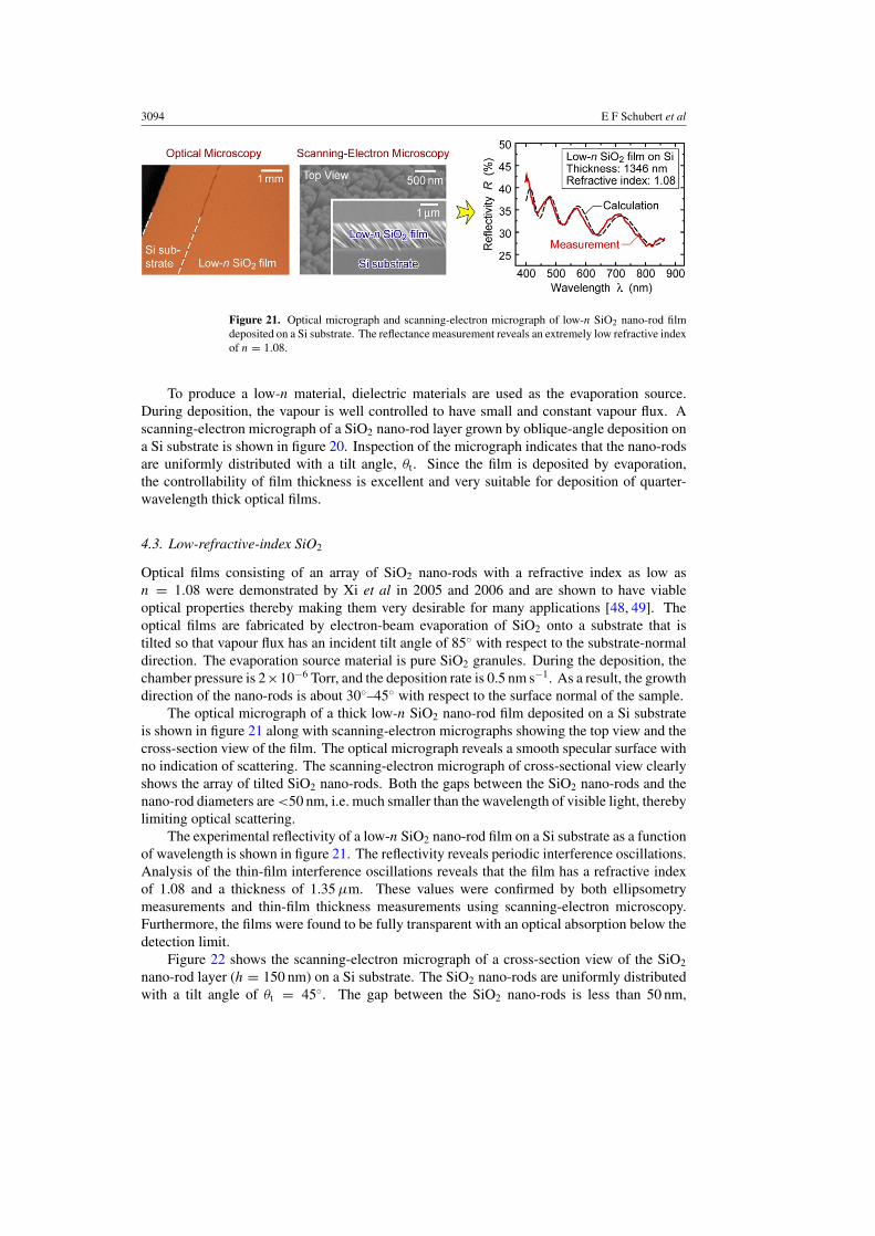
Figure 21. Optical micrograph and scanning-electron micrograph of low-n SiO2 nano-rod filmdeposited on a Si substrate. The reflectance measurement reveals an extremely low refractive indexof n = 1.08.
To produce a low-n material, dielectric materials are used as the evaporation source.During deposition, the vapour is well controlled to have small and constant vapour flux. Ascanning-electron micrograph of a SiO2 nano-rod layer grown by oblique-angle deposition ona Si substrate is shown in figure 20. Inspection of the micrograph indicates that the nano-rodsare uniformly distributed with a tilt angle, θt . Since the film is deposited by evaporation,the controllability of film thickness is excellent and very suitable for deposition of quarter-wavelength thick optical films.
4.3. Low-refractive-index SiO2
Optical films consisting of an array of SiO2 nano-rods with a refractive index as low asn = 1.08 were demonstrated by Xi et al in 2005 and 2006 and are shown to have viableoptical properties thereby making them very desirable for many applications [48, 49]. Theoptical films are fabricated by electron-beam evaporation of SiO2 onto a substrate that istilted so that vapour flux has an incident tilt angle of 85◦ with respect to the substrate-normaldirection. The evaporation source material is pure SiO2 granules. During the deposition, thechamber pressure is 2×10⁻⁶ Torr, and the deposition rate is 0.5 nm s−1. As a result, the growthdirection of the nano-rods is about 30◦–45◦ with respect to the surface normal of the sample.
The optical micrograph of a thick low-n SiO2 nano-rod film deposited on a Si substrateis shown in figure 21 along with scanning-electron micrographs showing the top view and thecross-section view of the film. The optical micrograph reveals a smooth specular surface withno indication of scattering. The scanning-electron micrograph of cross-sectional view clearlyshows the array of tilted SiO2 nano-rods. Both the gaps between the SiO2 nano-rods and thenano-rod diameters are <50 nm, i.e. much smaller than the wavelength of visible light, therebylimiting optical scattering.
The experimental reflectivity of a low-n SiO2 nano-rod film on a Si substrate as a functionof wavelength is shown in figure 21. The reflectivity reveals periodic interference oscillations.Analysis of the thin-film interference oscillations reveals that the film has a refractive indexof 1.08 and a thickness of 1.35 µm. These values were confirmed by both ellipsometrymeasurements and thin-film thickness measurements using scanning-electron microscopy.Furthermore, the films were found to be fully transparent with an optical absorption below thedetection limit.
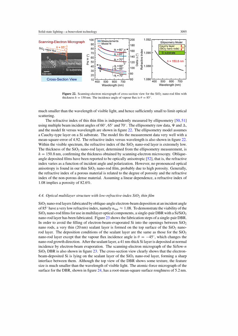
Figure 22 shows the scanning-electron micrograph of a cross-section view of the SiO2
nano-rod layer (h = 150 nm) on a Si substrate. The SiO2 nano-rods are uniformly distributedwith a tilt angle of θt = 45◦. The gap between the SiO2 nano-rods is less than 50 nm,
Solid-state lighting—a benevolent technology 3095
Figure 22. Scanning-electron micrograph of cross-section view for the SiO2 nano-rod film withthickness h = 150 nm. The incidence angle of vapour flux is θ = 85◦.
much smaller than the wavelength of visible light, and hence sufficiently small to limit opticalscattering.
The refractive index of this thin film is independently measured by ellipsometry [50, 51]using multiple beam incident angles of 60◦, 65◦ and 70◦. The ellipsometry raw data, and ,and the model fit versus wavelength are shown in figure 22. The ellipsometry model assumesa Cauchy-type layer on a Si substrate. The model fits the measurement data very well with amean-square-error of 4.92. The refractive index versus wavelength is also shown in figure 22.Within the visible spectrum, the refractive index of the SiO2 nano-rod layer is extremely low.The thickness of the SiO2 nano-rod layer, determined from the ellipsometry measurement, ish = 150.8 nm, confirming the thickness obtained by scanning-electron microscopy. Oblique-angle deposited films have been reported to be optically anisotropic [52], that is, the refractiveindex varies as a function of incident angle and polarization. However, no pronounced opticalanisotropy is found in our thin SiO2 nano-rod film, probably due to high porosity. Generally,the refractive index of a porous material is related to the degree of porosity and the refractiveindex of the non-porous dense material. Assuming a linear dependence, a refractive index of1.08 implies a porosity of 82.6%.
4.4. Optical multilayer structure with low-refractive-index SiO2 thin film
SiO2 nano-rod layers fabricated by oblique-angle electron-beam deposition at an incident angleof 85◦ have a very low refractive index, namely nlow ≈ 1.08. To demonstrate the viability of theSiO2 nano-rod films for use in multilayer optical components, a single-pair DBR with a Si/SiO2
nano-rod layer has been fabricated. Figure 23 shows the fabrication steps of a single-pair DBR.In order to avoid the filling of electron-beam-evaporated Si into the openings between SiO2
nano rods, a very thin (20 nm) sealant layer is formed on the top surface of the SiO2 nano-rod layer. The deposition conditions of the sealant layer are the same as those for the SiO2
nano-rod layer except that the vapour flux incidence angle is θ = −45◦, which changes thenano-rod growth direction. After the sealant layer, a 41 nm-thick Si layer is deposited at normalincidence by electron-beam evaporation. The scanning-electron micrograph of the Si/low-nSiO2 DBR is also shown in figure 23. The cross-section view clearly shows that the electron-beam-deposited Si is lying on the sealant layer of the SiO2 nano-rod layer, forming a sharpinterface between them. Although the top view of the DBR shows some texture, the featuresize is much smaller than the wavelength of visible light. The atomic-force micrograph of thesurface for the DBR, shown in figure 24, has a root-mean-square surface roughness of 5.2 nm.
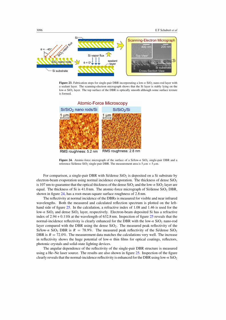
3096 E F Schubert et al
Figure 23. Fabrication steps for single-pair DBR incorporating a low-n SiO2 nano-rod layer witha sealant layer. The scanning-electron micrograph shows that the Si layer is stably lying on thelow-n SiO2 layer. The top surface of the DBR is optically smooth although some surface textureis formed.
Figure 24. Atomic-force micrograph of the surface of a Si/low-n SiO2 single-pair DBR and areference Si/dense SiO2 single-pair DBR. The measurement area is 5 µm × 5 µm.
For comparison, a single-pair DBR with Si/dense SiO2 is deposited on a Si substrate byelectron-beam evaporation using normal incidence evaporation. The thickness of dense SiO2
is 107 nm to guarantee that the optical thickness of the dense SiO2 and the low-n SiO2 layer areequal. The thickness of Si is 41.0 nm. The atomic-force micrograph of Si/dense SiO2 DBR,shown in figure 24, has a root-mean-square surface roughness of 2.8 nm.
The reflectivity at normal incidence of the DBRs is measured for visible and near infraredwavelengths. Both the measured and calculated reflection spectrum is plotted on the left-hand side of figure 25. In the calculation, a refractive index of 1.08 and 1.46 is used for thelow-n SiO2 and dense SiO2 layer, respectively. Electron-beam deposited Si has a refractiveindex of 2.94 + 0.110i at the wavelength of 632.8 nm. Inspection of figure 25 reveals that thenormal-incidence reflectivity is clearly enhanced for the DBR with the low-n SiO2 nano-rodlayer compared with the DBR using the dense SiO2. The measured peak reflectivity of theSi/low-n SiO2 DBR is R = 78.9%. The measured peak reflectivity of the Si/dense SiO2
DBR is R = 72.0%. The measurement data matches the calculations very well. The increasein reflectivity shows the huge potential of low-n thin films for optical coatings, reflectors,photonic crystals and solid-state lighting devices.
The angular dependence of the reflectivity of the single-pair DBR structure is measuredusing a He–Ne laser source. The results are also shown in figure 25. Inspection of the figureclearly reveals that the normal-incidence reflectivity is enhanced for the DBR using low-n SiO2

Solid-state lighting—a benevolent technology 3097
Figure 25. (a) Normal-incidence and (b) angular reflectivity of Si/low-n SiO2 single-pair DBR anda Si/dense SiO2 single-pair DBR on a Si substrate. The angular dependent reflectivity is measuredfor both the TE and TM polarizations at a wavelength of 632.8 nm.
nano-rod layer compared with the DBR using the dense SiO2. The experimental near-normal-incidence reflectivity is 78.8% and 69.8% for the DBR using the low-n and dense SiO2 films,respectively. The experimental results are in excellent agreement with the calculations.
5. Conclusions
In conclusion, the benefits of solid-state lighting in terms of energy savings, reduction ofenvironmental pollution and new functionalities are reviewed. Solid-state light sources arein the process of profoundly changing the way we generate light for general lighting andother applications. In contrast to conventional lighting sources, solid-state sources have thepotential to create light with unit power efficiency. Furthermore, the properties of light emittedby solid-state sources, such as spectral composition, polarization, colour temperature, temporalmodulation and far-field emission pattern, can be controlled to a degree that is impossible withconventional light sources such as incandescent and fluorescent lamps. The implications areenormous and, as a consequence, many positive developments are to be expected includinga reduction in global energy consumption, reduction of global-warming-gas and pollutantemissions and a multitude of new functionalities benefiting numerous applications. The impactof solid-state lighting technology on energy consumption and the environment is assessedin terms of a detailed yet fully transparent quantitative analysis. The impact on emergingapplication fields that make use of the controllability afforded by solid-state sources is discussedas well.
We also reviewed key technical areas that fuel continued progress in solid-state lighting.Specifically, we reviewed the use of novel phosphor distributions, namely remote phosphordistributions, in white LED lamps and show that remote phosphor distributions have higherefficiency and potentially higher reliability. We also reviewed the development of reflectorsin LEDs with emphasis on ‘perfect’ reflectors, i.e. reflectors with highly reflective omni-directional characteristics. Finally, we discussed a new class of thin-film materials withan unprecedented low refractive index. Such low-n materials may strongly contribute tocontinuous progress in solid-state lighting.

3098 E F Schubert et al
Acknowledgments
The authors gratefully acknowledge support by the National Science Foundation, ArmyResearch Office, Department of Energy, Sandia National Laboratory, New York State, SamsungCorporation and Crystal IS Corporation. The authors also acknowledge useful discussions withProfessors William N Gill, Shawn Y Lin, Toh-Ming Lu and Joel L Plawsky.
References
[1] Schubert E F and Kim J K 2005 Solid-state light sources getting smart Science 308 1274[2] Schubert E F 2006 Light-Emitting Diodes 2nd edn (Cambridge, UK: Cambridge University Press)[3] United States Energy Information Administration 2004 Annual energy review Report No. DOE/EIA-0384 and
http://www.eia.doe.gov/emeu/aer/elect.html[4] Bergh A, Craford M G, Duggal A and Haitz R 2001 The promise and challenge of solid-state lighting Phys.
Today 5544 42[5] US Department of Energy (DOE) 2006 Solid-State Lighting Research and Development Portfolio; Multi-year
program plan FY’07-FY’12 (Chicago: Navigant Consulting)[6] United States Energy Information Administration 1998 25th Anniversary of the 1973 Oil Embargo
http://www.eia.doe.gov/emeu/25opec/sld000.htm[7] Genet M, Villette S, Bourg-Heckly G and Loiseau S 2003 Development of a novel optical biopsy system
combining optical-fiber reflectance confocal imaging and confocal autofluorescence spectroscopy EuropeanConf. on Biomedical Optics (Munich, Germany, June 2003)
[8] Kutuza I B, Pozhar V E and Pustovoit V I 2003 AOTF-based imaging spectrometers for research of small-sizebiological objects Proc. SPIE 5143 165
[9] Brainard G C, Hanifin J P, Greeson J M, Byrne B, Glickman G, Gerner E and Rollag M D 2001 Action spectrumfor melatonin regulation in humans: evidence for a novel circadian photoreceptor J. Neurosci. 21 6405
[10] Blask D E, Dauchy R T, Sauer L A, Krause J A, Brainard G C 2003 Growth and fatty acid metabolism ofhuman breast cancer (MCF-7) xenografts in nude rats: impact of constant light-induced nocturnal melatoninsuppression Breast Cancer Res. Treat. 79 313
[11] Dowling J E 1987 The Retina (Cambridge, MA: Harvard University Press)[12] Carruthers J B 2002 Wireless infrared communications Wiley Encyclopedia of Telecommunications ed J G Proakis
(New York: Wiley)[13] Nhut D T, Takamura T, Watanabe H, Okamoto K and Tanaka M 2003 Responses of strawberry plantlets cultured
in vitro under super-bright red and blue light-emitting diodes (LEDs) Plant Cell Tissue Organ Culture 73 43Jao R C and Fang W 2003 An adjustable light source for photo-phyto related research and young plant production
Appl. Eng. Agric. 19 601[14] Chigrinov V G 1999 Electrooptic Effects in Liquid Crystal Materials (Norwood, MA: Artech House)[15] Nakamura S and Fasol G 1997 The Blue Laser Diode: GaN Based Light Emitters and Lasers (Berlin: Springer)[16] Mueller-Mach R, Mueller G O and Krames M R 2004 Phosphor materials and combinations for illumination
graded white pcLED Third Int. Conf. Solid State Lighting (San Diego CA, August 2003) Proc. SPIE 5187115
[17] Kim J K, Luo H, Schubert E F, Cho J, Sone C and Park Y 2005 Strongly enhanced phosphor efficiency in GaInNwhite light-emitting diodes using remote phosphor configuration and diffuse reflector cup Japan. J. Appl.Phys.—Express Lett. 44 L 649
[18] Luo H, Kim J K, Schubert E F, Cho J, Sone C and Park Y 2005 Analysis of high-power packages for phosphor-based white-light-emitting diodes Appl. Phys. Lett. 86 243505
[19] Kim J K, Gessmann T, Luo H and Schubert E F 2004 GaInN light-emitting diodes with RuO2/SiO2/Ag omni-directional reflector Appl. Phys. Lett. 84 4508
[20] Rayleigh L 1912 The problem of the whispering gallery Sci. Papers 5 617[21] Luo H, Kim J K, Xi Y, Schubert E F, Cho J, Sone C and Park Y 2006 Trapped whispering-gallery optical modes
in white light-emitting diode lamps with remote phosphor Appl. Phys. Lett. 89 041125[22] Schade H and Smith Z E 1985 Mie scattering and rough surfaces Appl. Opt. 24 3221[23] Xi Y, Li X, Mont F, Gessmann Th, Luo H and Schubert E F 2006 Quantitative assessment of diffusivity and
specularity of surface-textured reflectors for light extraction in light-emitting diodes J. Vac. Sci. Technol. A24 1627
[24] Gessmann T, Schubert E F, Graff J W, Streubel K and Karnutsch C 2003 Omnidirectional reflective contacts forlight-emitting diode IEEE Electron Device Lett. 24 683

Solid-state lighting—a benevolent technology 3099
[25] Gessmann T and Schubert E F 2004 High-efficiency AlGaInP light-emitting diodes for solid-state lightingapplications J. Appl. Phys. 95 2203
[26] Kim J K, Gessmann T, Luo H and Schubert E F 2004 GaInN light-emitting diodes with RuO2/SiO2/Ag omni-directional reflector Appl. Phys. Lett. 84 4508
[27] Born M and Wolf E 1987 Principle of Optics 6th edn (Oxford: Pergamon) p 62[28] Kim J K, Gessmann T, Schubert E F, Xi J-Q, Luo H, Cho J, Sone C, and Park Y 2004 GaInN light-emitting
diodes with conductive omnidirectional reflector having a low-refractive-index indium–tin oxide Appl. Phys.Lett. 88 013501
[29] Gessmann T, Li Y-L, Schubert E F, Graff J W and Sheu J K 2003 GaInN light-emitting diodes with omni-directional reflectors Proc. SPIE 4996 26
[30] Song J-O, Leem D-S, Kwak J S, Nam O H, Park Y, Seong T-Y 2003 Low-resistance and highly-reflective Zn–Nisolid solution/Ag ohmic contacts for flip-chip light-emitting diodes Appl. Phys. Lett. 83 4990
[31] Krames M R et al 1999 High-power truncated-inverted-pyramid (AlxGa1−x )0.5In0.5P/GaP light-emitting diodesexhibiting >50 external quantum efficiency Appl. Phys. Lett. 75 2365
[32] Gardner N F, Chui H C, Chen E I, Krames M R, Huang J-W, Kish F A, Kocot C P, Tan T S and Moll N 1999 1.4×improvement in transparent substrate light-emitting diodes (AlxGa1−x )0.5In0.5P/GaP with thin (�200 nm)active regions Appl. Phys. Lett. 74 2230
[33] Streubel K, Rapp S, André J and Chitica N 1996 1.26 µm vertical cavity laser with two InP/air-gap reflectorsElectron. Lett. 32 1369
[34] Ho S-T, McCall S L, Slusher R E, Pfeiffer L N, West K W, Levi A F J, Blonder G E and Jewell J L 1990 Highindex contrast mirrors for optical microcavities Appl. Phys. Lett. 57 1387
[35] Temelkuran B, Hart S D, Benoit G, Joannopoulos J D and Fink Y 2002 Wavelength-scalable hollow opticalfibres with large photonic bandgaps for CO2 laser transmission Nature 420 650
[36] Xi J-Q, Ojha M, Cho W, Plawsky J L, Gill W N, Gessmann T and Schubert E F 2005 Omnidirectional reflectorusing nanoporous SiO2 as a low-refractive-index material Opt. Lett. 30 1518
[37] Xi J-Q, Ojha M, Plawsky J L, Gill W N, Kim J K and Schubert E F 2005 Internal high reflectivity omni-directionalreflectors Appl. Phys. Lett. 87 031111
[38] Nitta S V, Pisupatti V, Jain A, Wayner P C Jr, Gill W N and Plawsky J L 1999 Surface modified spin-on xerogelfilms as interlayer dielectrics J. Vac. Sci. Technol. B 17 205
[39] Jain A, Rogojevic S, Ponoth S, Agarwal N, Matthew I, Gill W N, Persans P, Tomozawa M, Plawsky J L andSimonnyi E 2001 Porous silica materials as low-k dielectrics for electronic and optical interconnects ThinSolid Films 398–399 513
[40] Jain A, Rogojevic S, Ponoth S, Gill W N, Plawsky J L, Simonyi E, Chen S T and Ho P S 2002 Processingdependent thermal conductivity of nanoporous silica xerogel films J. Appl. Phys. 91 3275
[41] Gill W N, Plawsky J L and Xi J Q 2005 personal communication[42] Holland L 1953 The effect of vapor incidence on the structure of evaporated aluminum films J. Opt. Soc. Am.
43 376[43] Lakhtakia A and Messier R 2005 Sculptured Thin Films: Nanoengineered Morphology and Optics (Washington:
SPIE)[44] Robbie K, Friedrich L J, Dew S K, Smy T and Brett M J 1995 Fabrication of thin films with highly porous
microstructures J. Vac. Sci. Technol. A 13 1032[45] Abelmann L and Lodder C 1997 Oblique evaporation and surface diffusion Thin Solid Films 305 1[46] Robbie K and Brett M J 1997 Sculptured thin films and glancing angle deposition: growth mechanics and
applications J. Vac. Sci. Technol. A 15 1460[47] Vick D, Friedrich L J, Dew S K, Brett M J, Robbie K, Seto M and Smy T 1999 Self-shadowing and surface
diffusion effects in obliquely deposited thin films Thin Solid Films 339 88[48] Xi J-Q, Kim J K and Schubert E F 2005 Silica nanorod-array films with very low refractive indices Nano Lett.
5 1385[49] Xi J-Q, Kim J K, Schubert E F, Ye D, Lu T-M and Lin S-Y 2006 Very low-refractive-index optical thin films
consisting of an array of SiO2 nanorods Opt. Lett. 31 601[50] Woollam J A, Johs B, Herzinger C M, Hilfiker J, Synowicki R and Bungay C L 1999 Overview of variable angle
spectroscopic ellipsometry (VASE): I. Basic theory and typical applications Crit. Rev. Opt. Sci. Technol.CR72 3
[51] Johs B, Woollam J A, Herzinger C M, Hilfiker J, Synowicki R and Bungay C L 1999 Overview of VariableAngle Spectroscopic Ellipsometry (VASE): II. Advanced applications Crit. Rev. Opt. Sci. Technol. CR72 29
[52] Kaminska K and Robbie K 2004 Birefringent omnidirectional reflector Appl. Opt. 43 1570