solomon systech ssd1320 controller datasheet
TRANSCRIPT
Advance Information
160 x 160, 16 Gray Scale Dot Matrix OLED/PLED Segment/Common Driver with Controller
This document contains information on a new product. Specifications and information herein are subject to change without notice.
http://www.solomon-systech.com SSD1320 Rev 1.0 P 1/39 May 2017 Copyright 2017 Solomon Systech Limited
SSD1320
Solomon Systech May 2017 P 2/39 Rev 1.0 SSD1320
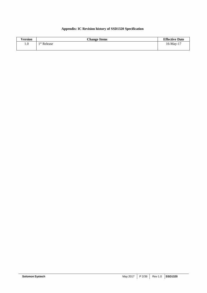
Appendix: IC Revision history of SSD1320 Specification
Version Change Items Effective Date 1.0 1st Release 16-May-17

SSD1320 Rev 1.0 P 3/39 May 2017 Solomon Systech
CONTENTS
1 GENERAL DESCRIPTION ....................................................................................................... 6
2 FEATURES .................................................................................................................................. 6
3 ORDERING INFORMATION .................................................................................................. 6
4 BLOCK DIAGRAM .................................................................................................................... 7
5 PIN DESCRIPTION .................................................................................................................... 8
6 FUNCTIONAL BLOCK DESCRIPTIONS ............................................................................... 11 6.1 MCU INTERFACE SELECTION ............................................................................................................................... 11
6.1.1 MCU Parallel 6800-series Interface ................................................................................................................ 11 6.1.2 MCU Parallel 8080-series Interface ................................................................................................................ 12 6.1.3 MCU Serial Interface (4-wire SPI) .............................................................................................................. 13 6.1.4 MCU Serial Interface (3-wire SPI) .............................................................................................................. 14 6.1.5 MCU I2C Interface ...................................................................................................................................... 15
6.2 COMMAND DECODER ........................................................................................................................................... 18 6.3 OSCILLATOR CIRCUIT AND DISPLAY TIME GENERATOR ....................................................................................... 18 6.4 FR SYNCHRONIZATION ......................................................................................................................................... 19 6.5 RESET CIRCUIT .................................................................................................................................................... 19 6.6 SEGMENT DRIVERS/COMMON DRIVERS ................................................................................................................ 20 6.7 GRAPHIC DISPLAY DATA RAM (GDDRAM) ............................................................................................................ 23 6.8 SEG/COM DRIVING BLOCK ................................................................................................................................. 28 6.9 POWER ON AND OFF SEQUENCE .......................................................................................................................... 29
7 MAXIMUM RATINGS ............................................................................................................ 30
8 DC CHARACTERISTICS........................................................................................................ 31
9 AC CHARACTERISTICS........................................................................................................ 32
10 APPLICATION EXAMPLE ................................................................................................. 38
Solomon Systech May 2017 P 4/39 Rev 1.0 SSD1320
TABLES TABLE 3-1: ORDERING INFORMATION .................................................................................................................................... 6 TABLE 5-1: PIN DESCRIPTION ................................................................................................................................................ 8 TABLE 5-2: BUS INTERFACE SELECTION ................................................................................................................................ 9 TABLE 6-1: MCU INTERFACE ASSIGNMENT UNDER DIFFERENT BUS INTERFACE MODE .......................................................... 11 TABLE 6-2: CONTROL PINS OF 6800 INTERFACE ................................................................................................................... 11 TABLE 6-3: CONTROL PINS OF 8080 INTERFACE ................................................................................................................... 13 TABLE 6-4: CONTROL PINS OF 4-WIRE SERIAL INTERFACE .................................................................................................... 13 TABLE 6-5: CONTROL PINS OF 3-WIRE SERIAL INTERFACE ................................................................................................... 14 TABLE 6-6: GDDRAM ADDRESS MAP 1............................................................................................................................... 23 TABLE 6-7: GDDRAM ADDRESS MAP 2............................................................................................................................... 24 TABLE 6-8: GDDRAM ADDRESS MAP 3 .............................................................................................................................. 25 TABLE 6-9: GDDRAM ADDRESS MAP 4............................................................................................................................... 26 TABLE 6-10: GDDRAM ADDRESS MAP 5 ............................................................................................................................ 27 TABLE 7-1: MAXIMUM RATINGS ......................................................................................................................................... 30 TABLE 8-1: DC CHARACTERISTICS ...................................................................................................................................... 31 TABLE 9-1: AC CHARACTERISTICS ...................................................................................................................................... 32 TABLE 9-2: 6800-SERIES MCU PARALLEL INTERFACE TIMING CHARACTERISTICS .............................................................. 33 TABLE 9-3: 8080-SERIES MCU PARALLEL INTERFACE TIMING CHARACTERISTICS ............................................................. 34 TABLE 9-4: SERIAL INTERFACE TIMING CHARACTERISTICS (4-WIRE SPI)............................................................................. 35 TABLE 9-5: SERIAL INTERFACE TIMING CHARACTERISTICS (3-WIRE SPI)............................................................................. 36 TABLE 9-6: I2C INTERFACE TIMING CHARACTERISTICS ........................................................................................................ 37

SSD1320 Rev 1.0 P 5/39 May 2017 Solomon Systech
FIGURES FIGURE 4-1 –SSD1320 BLOCK DIAGRAM .............................................................................................................................. 7 FIGURE 6-1: DATA READ BACK PROCEDURE - INSERTION OF DUMMY READ ......................................................................... 12 FIGURE 6-2: EXAMPLE OF WRITE PROCEDURE IN 8080 PARALLEL INTERFACE MODE ........................................................... 12 FIGURE 6-3: EXAMPLE OF READ PROCEDURE IN 8080 PARALLEL INTERFACE MODE ............................................................ 12 FIGURE 6-4: DISPLAY DATA READ BACK PROCEDURE - INSERTION OF DUMMY READ ........................................................... 13 FIGURE 6-5: WRITE PROCEDURE IN 4-WIRE SERIAL INTERFACE MODE ................................................................................. 14 FIGURE 6-6: WRITE PROCEDURE IN 3-WIRE SERIAL INTERFACE MODE ................................................................................. 14 FIGURE 6-7: I2C-BUS DATA FORMAT .................................................................................................................................... 16 FIGURE 6-8: DEFINITION OF THE START AND STOP CONDITION ........................................................................................... 17 FIGURE 6-9: DEFINITION OF THE ACKNOWLEDGEMENT CONDITION ..................................................................................... 17 FIGURE 6-10: DEFINITION OF THE DATA TRANSFER CONDITION ........................................................................................... 17 FIGURE 6-11: OSCILLATOR CIRCUIT AND DISPLAY TIME GENERATOR ................................................................................ 18 FIGURE 6-12: SEGMENT AND COMMON DRIVER BLOCK DIAGRAM ...................................................................................... 20 FIGURE 6-13: SEGMENT AND COMMON DRIVER SIGNAL WAVEFORM ................................................................................. 21 FIGURE 6-14: GRAY SCALE CONTROL BY PWM IN SEGMENT .............................................................................................. 22 FIGURE 6-15: IREF CURRENT SETTING BY RESISTOR VALUE ................................................................................................ 28 FIGURE 6-16: POWER ON SEQUENCE ................................................................................................................................... 29 FIGURE 6-17: POWER OFF SEQUENCE ................................................................................................................................. 29 FIGURE 9-1: 6800-SERIES MCU PARALLEL INTERFACE CHARACTERISTICS .......................................................................... 33 FIGURE 9-2: 8080-SERIES PARALLEL INTERFACE CHARACTERISTICS .................................................................................... 34 FIGURE 9-3: SERIAL INTERFACE CHARACTERISTICS (4-WIRE SPI) ........................................................................................ 35 FIGURE 9-4: SERIAL INTERFACE CHARACTERISTICS (3-WIRE SPI) ........................................................................................ 36 FIGURE 9-5: I2C INTERFACE TIMING CHARACTERISTICS ...................................................................................................... 37 FIGURE 10-1: APPLICATION EXAMPLE OF SSD1320Z .......................................................................................................... 38
Solomon Systech May 2017 P 6/39 Rev 1.0 SSD1320
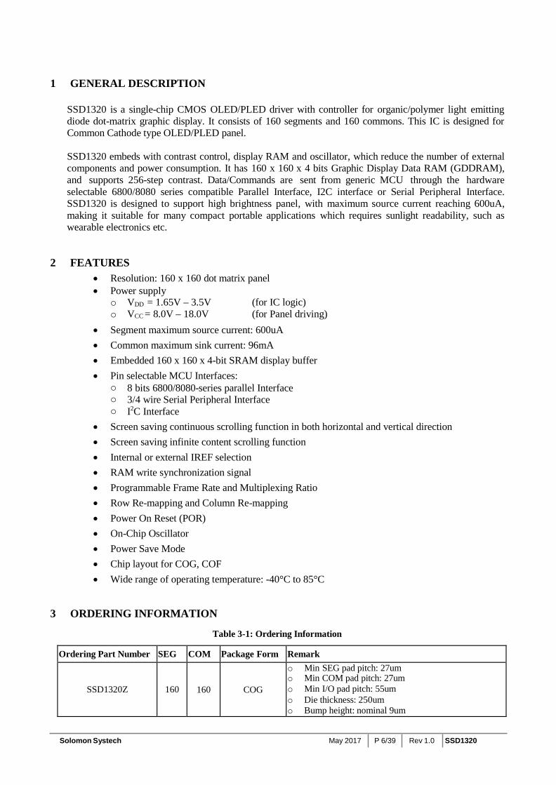
1 GENERAL DESCRIPTION
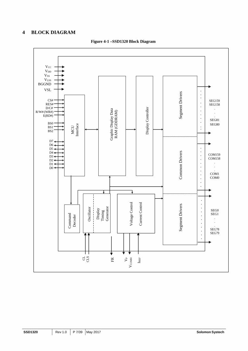
SSD1320 is a single-chip CMOS OLED/PLED driver with controller for organic/polymer light emitting diode dot-matrix graphic display. It consists of 160 segments and 160 commons. This IC is designed for Common Cathode type OLED/PLED panel.
SSD1320 embeds with contrast control, display RAM and oscillator, which reduce the number of external components and power consumption. It has 160 x 160 x 4 bits Graphic Display Data RAM (GDDRAM), and supports 256-step contrast. Data/Commands are sent from generic MCU through the hardware selectable 6800/8080 series compatible Parallel Interface, I2C interface or Serial Peripheral Interface. SSD1320 is designed to support high brightness panel, with maximum source current reaching 600uA, making it suitable for many compact portable applications which requires sunlight readability, such as wearable electronics etc.
2 FEATURES • Resolution: 160 x 160 dot matrix panel • Power supply
o VDD = 1.65V – 3.5V (for IC logic) o VCC = 8.0V – 18.0V (for Panel driving)
• Segment maximum source current: 600uA • Common maximum sink current: 96mA • Embedded 160 x 160 x 4-bit SRAM display buffer • Pin selectable MCU Interfaces:
o 8 bits 6800/8080-series parallel Interface o 3/4 wire Serial Peripheral Interface o I2C Interface
• Screen saving continuous scrolling function in both horizontal and vertical direction • Screen saving infinite content scrolling function • Internal or external IREF selection • RAM write synchronization signal • Programmable Frame Rate and Multiplexing Ratio • Row Re-mapping and Column Re-mapping • Power On Reset (POR) • On-Chip Oscillator • Power Save Mode • Chip layout for COG, COF • Wide range of operating temperature: -40°C to 85°C
3 ORDERING INFORMATION
Table 3-1: Ordering Information
Ordering Part Number SEG COM Package Form Remark
SSD1320Z
160
160
COG
o Min SEG pad pitch: 27um o Min COM pad pitch: 27um o Min I/O pad pitch: 55um o Die thickness: 250um o Bump height: nominal 9um
SSD1320 Rev 1.0 P 7/39 May 2017 Solomon Systech
VCC
VDD VSS VLSS
BGGND VSL
CS#
RES# D/C#
R/W# (WR#) E(RD#)
BS0 BS1 BS2
.
.
.
. SEG159
. SEG158
. .
. .
. .
. SEG81
. SEG80
.
D7 D6 D5 D4 D3 D2 D1 D0
.
.
. COM159
. COM158
. .
. .
. .
. COM1
. COM0
.
.
.
.
.
.
.
.
.
.
.
.
.
SEG0 SEG1
.
.
. SEG78 SEG79
4 BLOCK DIAGRAM
Figure 4-1 –SSD1320 Block Diagram
Se
gmen
t Driv
ers
C
omm
on D
river
s
Se
gmen
t Driv
ers
G
raph
ic D
ispl
ay D
ata
RA
M (G
DD
RA
M)
D
ispl
ay C
ontro
ller
M
CU
In
terfa
ce
Vol
tage
Con
trol
Cur
rent
Con
trol
Com
man
d D
ecod
er
CL
CLS
Osc
illat
or
Dis
play
Ti
min
g G
ener
ator
FR
VP
VCO
MH
I REF

Solomon Systech May 2017 P 8/39 Rev 1.0 SSD1320
5 PIN DESCRIPTION
Key: I = Input NC = Not Connected O =Output Pull LOW= connect to Ground I/O = Bi-directional (input/output) Pull HIGH= connect to VDD
P = Power pin
Table 5-1: Pin Description
Pin Name Pin Type Description VDD P Power supply pin for core logic operation.
VCC P Power supply for panel driving voltage. This is also the most positive power voltage supply pin.
BGGND P Reserved pin. It must be connected to ground.
VSS P Ground pin. It must be connected to external ground.
VLSS P Analog system ground pin. It must be connected to external ground.
VSL P This is segment voltage (output low level) reference pin. When external VSL is not used, this pin should be connected to VLSS externally. When external VSL is used, this pin should be connected with resistor and diode to ground (details depends on application).
VLH P Logic high (same voltage level as VDD) for internal connection of input and I/O pins. No need to connect to external power source.
VLL P Logic low (same voltage level as VSS) for internal connection of input and I/O pins. No need to connect to external ground.
VCOMH P COM signal deselected voltage level. A capacitor should be connected between this pin and VSS.
VP P This pin is the segment pre-charge voltage reference pin. A capacitor should be connected between this pin and VSS to enhance pre-charge voltage stability if necessary. When external capacitor is not used, this pin should be kept NC. No external power supply is allowed to connect to this pin.
VBREF O This is a reserved pin. It should be kept NC.
IREF I This pin is the segment output current reference pin. IREF is supplied externally. A resistor should be connected between this pin and VSS to maintain the current around 10uA. Please refer to Figure 6-15 for the details of resistor value. When internal IREF is used, this pin should be kept NC.

Pin Name Pin Type Description BS[2:0] I MCU bus interface selection pins. Select appropriate logic setting as described in the
following table. BS2, BS1 and BS0 are pin select.
Table 5-2: Bus Interface selection BS[2:0] Interface 000 4-line SPI 001 3-line SPI 010 I2C 110 8-bit 8080 parallel 100 8-bit 6800 parallel
Note (1) 0 is connected to VSS (2) 1 is connected to VDD
CL I This is external clock input pin. When internal clock is enabled (i.e. HIGH in CLS pin), this pin is not used and should be connected to VSS. When internal clock is disabled (i.e. LOW in CLS pin), this pin is the external clock source input pin.
CLS I This is internal clock enable pin. When it is pulled HIGH (i.e. connect to VDD), internal clock is enabled. When it is pulled LOW, the internal clock is disabled; an external clock source must be connected to the CL pin for normal operation.
CS# I This pin is the chip select input connecting to the MCU. The chip is enabled for MCU communication only when CS# is pulled LOW (active LOW).
RES# I This pin is reset signal input. When the pin is pulled LOW, initialization of the chip is executed. Keep this pin pull HIGH during normal operation.
D/C# I This pin is Data/Command control pin connecting to the MCU. When the pin is pulled HIGH, the data at D[7:0] will be interpreted as data. When the pin is pulled LOW, the data at D[7:0] will be transferred to a command register. In I2C mode, this pin acts as SA0 for slave address selection. When 3-wire serial interface is selected, this pin must be connected to VSS. For detail relationship to MCU interface signals, refer to Timing Characteristics Diagrams at Figure 9-3
R/W# (WR#) I This pin is read / write control input pin connecting to the MCU interface. When 6800 interface mode is selected, this pin will be used as Read/Write (R/W#) selection input. Read mode will be carried out when this pin is pulled HIGH and write mode when LOW. When 8080 interface mode is selected, this pin will be the Write (WR#) input. Data write operation is initiated when this pin is pulled LOW and the chip is selected. When serial or I2C interface is selected, this pin must be connected to VSS.
SSD1320 Rev 1.0 P 9/39 May 2017 Solomon Systech

Pin Name Pin Type Description E (RD#) I This pin is MCU interface input.
When 6800 interface mode is selected, this pin will be used as the Enable (E) signal. Read/write operation is initiated when this pin is pulled HIGH and the chip is selected. When 8080 interface mode is selected, this pin receives the Read (RD#) signal. Read operation is initiated when this pin is pulled LOW and the chip is selected. When serial or I2C interface is selected, this pin must be connected to VSS.
D[7:0] I/O These pins are bi-directional data bus connecting to the MCU data bus. Unused pins are recommended to tie LOW. When serial interface mode is selected, D2, D1 should be tied together as the serial data input: SDIN, and D0 will be the serial clock input: SCLK. When I2C mode is selected, D2, D1 should be tied together and serve as SDAout, SDAin in application and D0 is the serial clock input, SCL.
FR O This pin outputs RAM write synchronization signal. Proper timing between MCU data writing and frame display timing can be achieved to prevent tearing effect. It should be kept NC if it is not used.
T0 I/O This is a reserved pin. It should be kept NC.
T1 I/O This is a reserved pin. It should be kept NC.
SEG0 ~ SEG159
O These pins provide the OLED segment driving signals. These pins are VSS state when display is OFF.
COM0 ~ COM159
O These pins provide the Common switch signals to the OLED panel. These pins are in high impedance state when display is OFF.
TR[15:0] - Reserved pin and is recommended to keep it float.
NC - This is dummy pin. It should be kept NC.
Solomon Systech May 2017 P 10/39 Rev 1.0 SSD1320

SSD1320 Rev 1.0 P 11/39 May 2017 Solomon Systech
6 FUNCTIONAL BLOCK DESCRIPTIONS
6.1 MCU Interface selection SSD1320 MCU interface consist of 8 data pins and 5 control pins. The pin assignment at different interface mode is summarized in Table 6-1. Different MCU mode can be set by hardware selection on BS[2:0] pins (please refer to Table 5-2 for BS[2:0] setting).
Table 6-1: MCU interface assignment under different bus interface mode
Pin Name Bus Interface
Data/Command Interface Control Signal
D7 D6 D5 D4 D3 D2 D1 D0 E R/W# CS# D/C# RES# 8-bit 8080 D[7:0] RD# WR# CS# D/C# RES# 8-bit 6800 D[7:0] E R/W# CS# D/C# RES# 3-wire SPI Tie LOW SDIN SCLK Tie LOW CS# Tie LOW RES# 4-wire SPI Tie LOW SDIN SCLK Tie LOW CS# D/C# RES# I2C Tie LOW SDAOUT SDAIN SCL Tie LOW SA0 RES#
When serial interface mode is selected, D0 will be the serial clock input: SCLK; D1 and D2 should be tied together as the serial data input: SDIN.
6.1.1 MCU Parallel 6800-series Interface The parallel interface consists of 8 bi-directional data pins (D[7:0]), R/W#, D/C#, E and CS#.
A LOW in R/W# indicates WRITE operation and HIGH in R/W# indicates READ operation. A LOW in D/C# indicates COMMAND read/write and HIGH in D/C# indicates DATA read/write. The E input serves as data latch signal while CS# is LOW. Data is latched at the falling edge of E signal.
Table 6-2: Control pins of 6800 interface
Function E R/W# CS# D/C#
Write command ↓ L L L
Read status ↓ H L L
Write data ↓ L L H
Read data ↓ H L H
Note (1) ↓ stands for falling edge of signal
H stands for HIGH in signal L stands for LOW in signal
In order to match the operating frequency of display RAM with that of the microprocessor, some pipeline processing is internally performed which requires the insertion of a dummy read before the first actual display data read. This is shown in Figure 6-1.

Solomon Systech May 2017 P 12/39 Rev 1.0 SSD1320
Figure 6-1: Data read back procedure - insertion of dummy read
R/W#
E
Databus
Write column address
Dummy read
Read 1st data
Read 2nd data Read 3rd data
6.1.2 MCU Parallel 8080-series Interface The parallel interface consists of 8 bi-directional data pins (D[7:0]), RD#, WR#, D/C# and CS#.
A LOW in D/C# indicates COMMAND read/write and HIGH in D/C# indicates DATA read/write. A rising edge of RD# input serves as a data READ latch signal while CS# is kept LOW. A rising edge of WR# input serves as a data/command WRITE latch signal while CS# is kept LOW.
Figure 6-2: Example of Write procedure in 8080 parallel interface mode
CS#
WR#
D[7:0]
D/C# RD#
high
low
Figure 6-3: Example of Read procedure in 8080 parallel interface mode
CS#
RD#
D[7:0]
D/C#
high WR#
low
N n n+1 n+2

SSD1320 Rev 1.0 P 13/39 May 2017 Solomon Systech
Table 6-3: Control pins of 8080 interface
Function RD# WR# CS# D/C# Write command H ↑ L L Read status ↑ H L L Write data H ↑ L H Read data ↑ H L H
Note (1) ↑ stands for rising edge of signal (2) H stands for HIGH in signal (3) L stands for LOW in signal
In order to match the operating frequency of display RAM with that of the microprocessor, some pipeline processing is internally performed which requires the insertion of a dummy read before the first actual display data read. This is shown in Figure 6-4.
Figure 6-4: Display data read back procedure - insertion of dummy read
WR#
RD#
Databus N n n+1 n+2
Write column address
Dummy read
Read 1st data
Read 2nd data Read 3rd data
6.1.3 MCU Serial Interface (4-wire SPI)
The 4-wire serial interface consists of serial clock: SCLK, serial data: SDIN, D/C#, CS#. In 4-wire SPI mode, D0 acts as SCLK, D1 and D2 are tied together to act as SDIN. For the unused data pins from D3 to D7, E(RD#) and R/W#(WR#) can be connected to an external ground.
Table 6-4: Control pins of 4-wire Serial interface
Function E R/W# CS# D/C# D0 Write command Tie LOW Tie LOW L L ↑ Write data Tie LOW Tie LOW L H ↑
Note (1) H stands for HIGH in signal (2) L stands for LOW in signal (3) ↑ stands for rising edge of signal
SDIN is shifted into an 8-bit shift register on every rising edge of SCLK in the order of D7, D6, ..., D0. D/C# is sampled on every eighth clock and D/C# should be kept stable throughout eight clock period. The data byte in the shift register is written to the Graphic Display Data RAM (GDDRAM) or command register in the same clock.
Under serial mode, only write operations are allowed.
Solomon Systech May 2017 P 14/39 Rev 1.0 SSD1320
Figure 6-5: Write procedure in 4-wire Serial interface mode
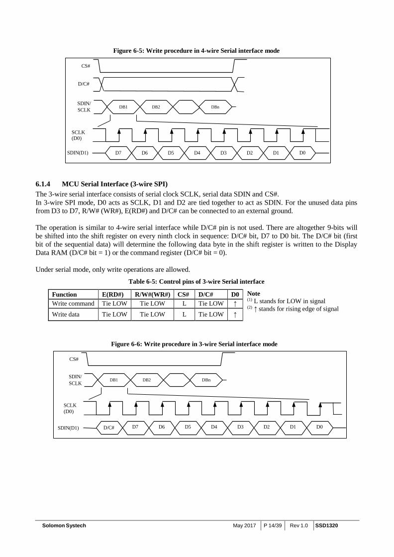
6.1.4 MCU Serial Interface (3-wire SPI) The 3-wire serial interface consists of serial clock SCLK, serial data SDIN and CS#. In 3-wire SPI mode, D0 acts as SCLK, D1 and D2 are tied together to act as SDIN. For the unused data pins from D3 to D7, R/W# (WR#), E(RD#) and D/C# can be connected to an external ground.
The operation is similar to 4-wire serial interface while D/C# pin is not used. There are altogether 9-bits will be shifted into the shift register on every ninth clock in sequence: D/C# bit, D7 to D0 bit. The D/C# bit (first bit of the sequential data) will determine the following data byte in the shift register is written to the Display Data RAM (D/C# bit = 1) or the command register (D/C# bit = 0).
Under serial mode, only write operations are allowed.
Table 6-5: Control pins of 3-wire Serial interface
Note (1) L stands for LOW in signal (2) ↑ stands for rising edge of signal
Figure 6-6: Write procedure in 3-wire Serial interface mode
CS#
SDIN/ SCLK
DB1 DB2 DBn
SCLK (D0)
SDIN(D1) D/C# D7 D6 D5 D4 D3 D2 D1 D0
CS# D/C#
SDIN/ SCLK DB1 DB2 DBn
SCLK (D0)
SDIN(D1) D7 D6 D5 D4 D3 D2 D1 D0
Function E(RD#) R/W#(WR#) CS# D/C# D0 Write command Tie LOW Tie LOW L Tie LOW ↑ Write data Tie LOW Tie LOW L Tie LOW ↑

SSD1320 Rev 1.0 P 15/39 May 2017 Solomon Systech
6.1.5 MCU I2C Interface The I2C communication interface consists of slave address bit SA0, I2C-bus data signal SDA (SDAOUT/D2 for output and SDAIN/D1 for input) and I2C-bus clock signal SCL (D0). Both the data and clock signals must be connected to pull-up resistors. RES# is used for the initialization of device.
a) Slave address bit (SA0)
SSD1320 has to recognize the slave address before transmitting or receiving any information by the I2C-bus. The device will respond to the slave address following by the slave address bit (“SA0” bit) and the read/write select bit (“R/W#” bit) with the following byte format,
b7 b6 b5 b4 b3 b2 b1 b0
0 1 1 1 1 0 SA0 R/W#
“SA0” bit provides an extension bit for the slave address. Either “0111100” or “0111101”, can be selected as the slave address of SSD1320. D/C# pin acts as SA0 for slave address selection. “R/W#” bit is used to determine the operation mode of the I2C-bus interface. R/W#=1, it is in read mode. R/W#=0, it is in write mode.
b) I2C-bus data signal (SDA) SDA acts as a communication channel between the transmitter and the receiver. The data and the acknowledgement are sent through the SDA.
It should be noticed that the ITO track resistance and the pulled-up resistance at “SDA” pin becomes a voltage potential divider. As a result, the acknowledgement would not be possible to attain a valid logic 0 level in “SDA”.
“SDAIN” and “SDAOUT” are tied together and serve as SDA. The “SDAIN” pin must be connected to act as SDA. The “SDAOUT” pin may be disconnected. When “SDAOUT” pin is disconnected, the acknowledgement signal will be ignored in the I2C-bus.
c) I2C-bus clock signal (SCL) The transmission of information in the I2C-bus is following a clock signal, SCL. Each transmission of data bit is taken place during a single clock period of SCL.

Solomon Systech May 2017 P 16/39 Rev 1.0 SSD1320
0 1 1 1 1
MSB ………………. LSB
D/C
# C
o AC
K
ACK
6.1.5.1 I2C-bus Write data The I2C-bus interface gives access to write data and command into the device. Please refer to Figure 6-7 for the write mode of I2C-bus in chronological order.
Figure 6-7: I2C-bus data format
Write mode
Note: Co – Continuation bit
D/C# – Data / Command Selection bit ACK – Acknowledgement SA0 – Slave address bit R/W# – Read / Write Selection bit S – Start Condition / P – Stop Condition
0 1 1 1 1 0
Control byte Data byte Control byte
Data byte
Slave Address m ≥ 0 words
1 byte
n ≥ 0 bytes
6.1.5.2 Write mode for I2C 1) The master device initiates the data communication by a start condition. The definition of the start
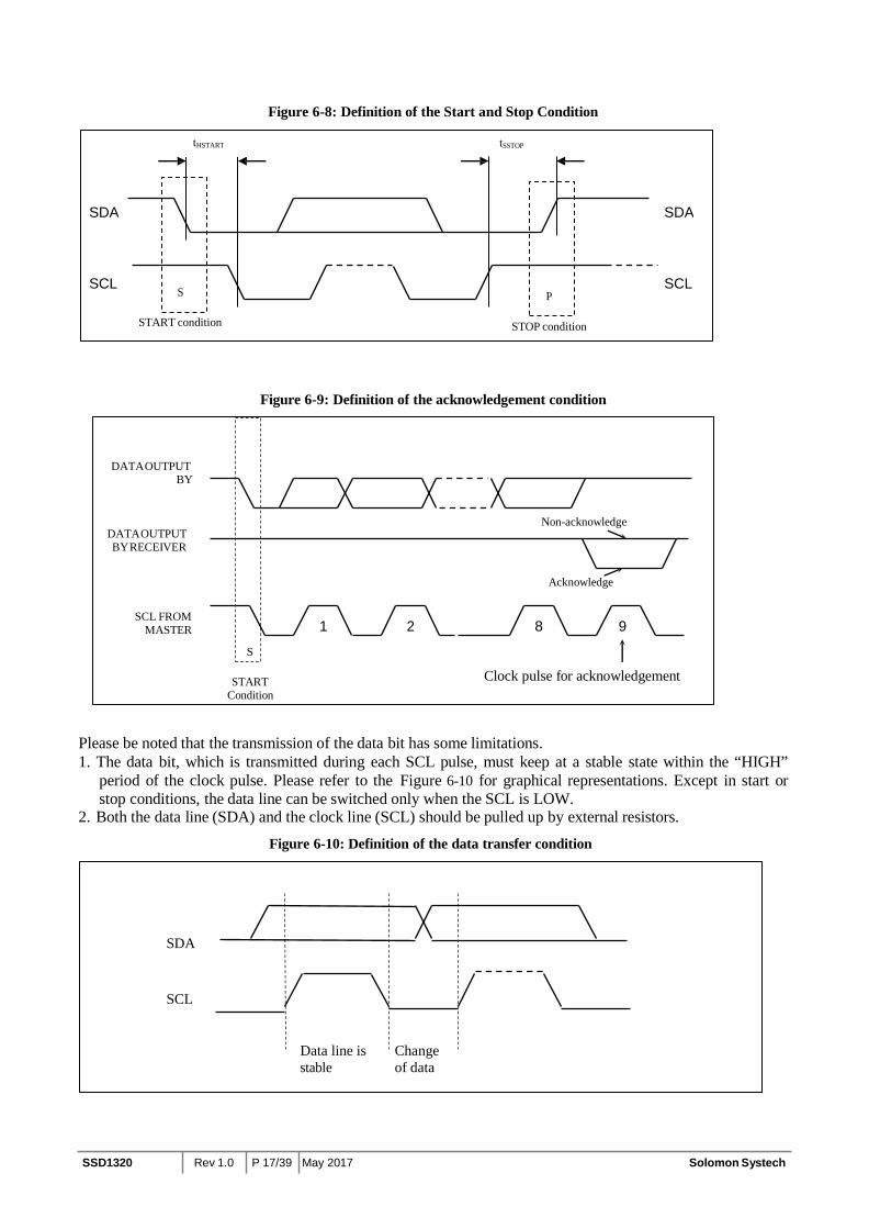
condition is shown in Figure 6-8. The start condition is established by pulling the SDA from HIGH to LOW while the SCL stays HIGH.
2) The slave address is following the start condition for recognition use. For the SSD1320, the slave address is either “b0111100” or “b0111101” by changing the SA0 to LOW or HIGH (D/C pin acts as SA0).
3) The write mode is established by setting the R/W# bit to logic “0”. 4) An acknowledgement signal will be generated after receiving one byte of data, including the slave
address and the R/W# bit. Please refer to the Figure 6-9 : Definition of the acknowledgement condition for the graphical representation of the acknowledge signal. The acknowledge bit is defined as the SDA line is pulled down during the HIGH period of the acknowledgement related clock pulse.
5) After the transmission of the slave address, either the control byte or the data byte may be sent across the SDA. A control byte mainly consists of Co and D/C# bits following by six “0” ‘s.
a. If the Co bit is set as logic “0”, the transmission of the following information will contain data bytes only.
b. The D/C# bit determines the next data byte is acted as a command or a data. If the D/C# bit is set to logic “0”, it defines the following data byte as a command. If the D/C# bit is set to logic “1”, it defines the following data byte as a data which will be stored at the GDDRAM. The GDDRAM column address pointer will be increased by one automatically after each data write.
6) Acknowledge bit will be generated after receiving each control byte or data byte. 7) The write mode will be finished when a stop condition is applied. The stop condition is also defined
in Figure 6-8. The stop condition is established by pulling the “SDA in” from LOW to HIGH while the “SCL” stays HIGH.
P ACK
ACK
D/C
# C
o AC
K R/W
# SA0
S
SSD1320 Rev 1.0 P 17/39 May 2017 Solomon Systech
Figure 6-8: Definition of the Start and Stop Condition
Figure 6-9: Definition of the acknowledgement condition
DATA OUTPUT BY
DATA OUTPUT BY RECEIVER
Non-acknowledge
Acknowledge
SCL FROM
MASTER
1 S
START
Condition
2 8 9
Clock pulse for acknowledgement
Please be noted that the transmission of the data bit has some limitations. 1. The data bit, which is transmitted during each SCL pulse, must keep at a stable state within the “HIGH”
period of the clock pulse. Please refer to the Figure 6-10 for graphical representations. Except in start or stop conditions, the data line can be switched only when the SCL is LOW.
2. Both the data line (SDA) and the clock line (SCL) should be pulled up by external resistors. Figure 6-10: Definition of the data transfer condition
SDA
SCL
Data line is Change stable of data
tHSTART tSSTOP
SDA SDA
SCL S SCL P
START condition STOP condition

Solomon Systech May 2017 P 18/39 Rev 1.0 SSD1320
6.2 Command Decoder This module determines whether the input data is interpreted as data or command. Data is interpreted based upon the input of the D/C# pin.
If D/C# pin is HIGH, D[7:0] is interpreted as display data written to Graphic Display Data RAM (GDDRAM). If it is LOW, the input at D[7:0] is interpreted as a command. Then data input will be decoded and written to the corresponding command register.
6.3 Oscillator Circuit and Display Time Generator Figure 6-11: Oscillator Circuit and Display Time Generator
Internal Oscillator
Fosc
CL
Divider
DCLK
Display Clock
CLS
This module is an on-chip LOW power RC oscillator circuitry. The operation clock (CLK) can be generated either from internal oscillator or external source CL pin. This selection is done by CLS pin. If CLS pin is pulled HIGH, internal oscillator is chosen and CL should be connected to VSS. Pulling CLS pin LOW disables internal oscillator and external clock must be connected to CL pins for proper operation. When the internal oscillator is selected, its output frequency Fosc can be changed by command D5h A[7:4].
The display clock (DCLK) for the Display Timing Generator is derived from CLK. The division factor “D” can be programmed from 1 to 256 by command D5h
DCLK = FOSC / D
The frame frequency of display is determined by the following formula.
where
FFRM = Fosc
D× K × No. of Mux
• D stands for clock divide ratio. It is set by command D5h A[3:0]. The divide ratio has the range from 1 to 256.
• K is the number of display clocks per row. The value is derived by K = Phase 1 period + Phase 2 period + Ko
= 7 + 2 + 66 = 75 at power on reset (that is K0 is a constant that equals to 66) Please refer to Section 6.6 for the details of the “Phase”.
• Number of multiplex ratio is set by command A8h. The power on reset value is 159 (i.e. 160MUX). • FOSC is the oscillator frequency. It can be changed by command D5h A[7:4]. The higher the register
setting results in higher frequency.
M U X
CLK
SSD1320 Rev 1.0 P 19/39 May 2017 Solomon Systech
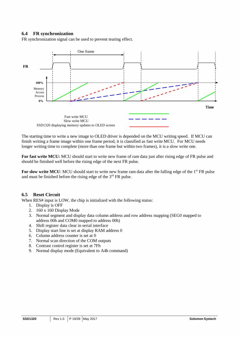
6.4 FR synchronization FR synchronization signal can be used to prevent tearing effect.
FR
Time
Fast write MCU Slow write MCU
SSD1320 displaying memory updates to OLED screen
The starting time to write a new image to OLED driver is depended on the MCU writing speed. If MCU can finish writing a frame image within one frame period, it is classified as fast write MCU. For MCU needs longer writing time to complete (more than one frame but within two frames), it is a slow write one.
For fast write MCU: MCU should start to write new frame of ram data just after rising edge of FR pulse and should be finished well before the rising edge of the next FR pulse.
For slow write MCU: MCU should start to write new frame ram data after the falling edge of the 1st FR pulse and must be finished before the rising edge of the 3rd FR pulse.
6.5 Reset Circuit When RES# input is LOW, the chip is initialized with the following status:
1. Display is OFF 2. 160 x 160 Display Mode 3. Normal segment and display data column address and row address mapping (SEG0 mapped to
address 00h and COM0 mapped to address 00h) 4. Shift register data clear in serial interface 5. Display start line is set at display RAM address 0 6. Column address counter is set at 0 7. Normal scan direction of the COM outputs 8. Contrast control register is set at 7Fh 9. Normal display mode (Equivalent to A4h command)
One frame
100%
Memory Access
Process 0%

Solomon Systech May 2017 P 20/39 Rev 1.0 SSD1320
6.6 Segment Drivers/Common Drivers
Segment drivers have 160 current sources to drive OLED panel. The driving current can be adjusted up to 600uA with 8 bits, 256 steps by contrast setting command (81h). Common drivers generate voltage scanning pulses. The block diagrams and waveforms of the segment and common driver are shown as follow.
Figure 6-12: Segment and Common Driver Block Diagram
VCC
ISEG
VCOMH
Non-select
Row
Current Drive
Selected Row
VLSS
OLED Pixel
VLSS
Segment Driver
Reset
Common Driver
The commons are scanned sequentially, row by row. If a row is not selected, all the pixels on the row are in reverse bias by driving those commons to voltage VCOMH as shown in Figure 6-13.
In the scanned row, the pixels on the row will be turned ON or OFF by sending the corresponding data signal to the segment pins.

SSD1320 Rev 1.0 P 21/39 May 2017 Solomon Systech
Figure 6-13: Segment and Common Driver Signal Waveform
COM0 VCOMH
VLSS
COM1 VCOMH
VLSS
COM Voltage
This row is selected to turn on
VCOMH
VLSS
Segment Voltage
Time
Waveform for ON
VP
VLSS Waveform for OFF
Time
One Frame Period Non-selected Row
Selected Row

Solomon Systech May 2017 P 22/39 Rev 1.0 SSD1320
There are four phases to driving an OLED a pixel. In phase 1, the pixel is reset by the segment driver to VLSS
in order to discharge the previous data charge stored in the parasitic capacitance along the segment electrode. The period of phase 1 can be programmed by command D9h A[3:0]. An OLED panel with larger capacitance requires a longer period for discharging.
In phase 2, first pre-charge is performed. The pixel is driven to attain the corresponding voltage level VP from VLSS. The amplitude of VP can be programmed by the command BCh. The period of phase 2 can be programmed by command D9h A[7:4]. If the capacitance value of the pixel of OLED panel is larger, a longer period is required to charge up the capacitor to reach the desired voltage.
In phase 3, the OLED pixel is driven to the targeted driving voltage through second pre-charge. The second pre-charge can control the speed of the charging process. The period of phase 3 can be programmed by command DCh.
Last phase (phase 4) is current drive stage. The current source in the segment driver delivers constant current to the pixel. The driver IC employs PWM (Pulse Width Modulation) method to control the gray scale of each pixel individually. The gray scale can be programmed into different Gamma settings by command BEh/BFh. The bigger gamma setting (the wider pulse widths) in the current drive stage results in brighter pixels and vice versa. This is shown in the following figure.
Figure 6-14: Gray Scale Control by PWM in Segment
Segment Voltage
Phase1
Phase2 Phase3
Phase4
VP
VLSS
Wider pulse width drives pixel brighter
OLED Panel
After finishing phase 4, the driver IC will go back to phase 1 to display the next row image data. This four- step cycle is run continuously to refresh image display on OLED panel.
The length of phase 4 is defined by command BEh/BFh. In the table, the gray scale is defined in incremental way, with reference to the length of previous table entry.

SSD1320 Rev 1.0 P 23/39 May 2017 Solomon Systech
6.7 Graphic Display Data RAM (GDDRAM)
The GDDRAM is a bit mapped static RAM holding the bit pattern to be displayed. The size of the RAM is 160x160x4 bits. For mechanical flexibility, re-mapping on both Segment and Common outputs can be selected by software. The GDDRAM address maps in Table 6-6 to Table 6-10 show some examples to re-map the GDDRAM. In the following tables, the lower nibble and higher nibble of D0, D1, D2 … D12797, D12798, D12799 represent the 160x160 data bytes in the GDDRAM.
These are the commands for Re-map setting:
Table 6-6 shows the GDDRAM map under the following condition: • Command Setting:
• Display Start Line=00h • Data byte sequence: D0, D1, D2 … D12799
Table 6-6: GDDRAM address map 1
Description Type Register Disable/Enable Column Address Re-map Single Byte A0h/A1h Horizontal/Vertical Address Increment Double Byte 20h 00h/01h Disable/Enable COM Re-map Single Byte C0h/C8h Disable/Enable Portrait Mode Double Byte 25h 00h/01h
Disable Column Address Re-map A0h Horizontal Address Increment 20h 00h Disable COM Re-map C0h Disable Portrait Mode 25h 00h

Solomon Systech May 2017 P 24/39 Rev 1.0 SSD1320
GS IC V e r ti c a l A d d r e s s i n g M o d e ( 4 - b i t GS m o d e )
S0 S1 S2 S3 … … S158 S159 COM159 COM158 COM157 COM156
:
:
:
COM5 COM4 COM3 COM2 COM1 COM0
S0 S1 S2 S3 … … S158 S159
Table 6-7 shows the GDDRAM map under the following condition: • Command Setting:
• Display Start Line=00h • Data byte sequence: D0, D1, D2 … D12799
Table 6-7: GDDRAM address map 2
D12645[3:0] D12645[7:4] D12644[3:0] D12644[7:4] D12643[3:0] D12643[7:4] D12642[3:0] D12642[7:4] D12641[3:0] D12641[7:4] D12640[3:0] D12640[7:4]
D5[3:0] D5[7:4] D165[3:0] D165[7:4] D4[3:0] D4[7:4] D164[3:0] D164[7:4] D3[3:0] D3[7:4] D163[3:0] D163[7:4] D2[3:0] D2[7:4] D162[3:0] D162[7:4] D1[3:0] D1[7:4] D161[3:0] D161[7:4] D0[3:0] D0[7:4] D160[3:0] D160[7:4]
D12799[3:0] D12799[7:4] D12798[3:0] D12798[7:4] D12797[3:0] D12797[7:4] D12796[3:0] D12796[7:4]
D159[3:0] D159[7:4] D319[3:0] D319[7:4] D158[3:0] D158[7:4] D318[3:0] D318[7:4] D157[3:0] D157[7:4] D317[3:0] D317[7:4] D156[3:0] D156[7:4] D316[3:0] D316[7:4]
Disable Column Address Re-map A0h Vertical Address Increment 20h 01h Disable COM Re-map C0h Disable Portrait Mode 25h 00h

SSD1320 Rev 1.0 P 25/39 May 2017 Solomon Systech
GS IC H o r i z o n ta l A d d r e s s i n g M o d e ( 4 - b i t GS m o d e ) w i th C o l u m n R e m a p
S0 S1 … … S156 S157 S158 S159
COM159 COM158 COM157 COM156
: : :
COM5 COM4 COM3 COM2 COM1 COM0
S0 S1 … … S156 S157 S158 S159
Table 6-8 shows the GDDRAM map under the following condition: • Command Setting:
• Display Start Line=00h • Data byte sequence: D0, D1, D2 … D12799
Table 6-8: GDDRAM address map 3
D401[7:4] D401[3:0] D400[7:4] D400[3:0] D321[7:4] D321[3:0] D320[7:4] D320[3:0] D241[7:4] D241[3:0] D240[7:4] D240[3:0] D161[7:4] D161[3:0] D160[7:4] D160[3:0] D81[7:4] D81[3:0] D80[7:4] D80[3:0] D1[7:4] D1[3:0] D0[7:4] D0[3:0]
D479[7:4] D479[3:0] D399[7:4] D399[3:0] D319[7:4] D319[3:0] D239[7:4] D239[3:0] D159[7:4] D159[3:0] D79[7:4] D79[3:0]
D12721[7:4] D12721[3:0] D12720[7:4] D12720[3:0] D12641[7:4] D12641[3:0] D12640[7:4] D12640[3:0] D12561[7:4] D12561[3:0] D12560[7:4] D12560[3:0] D12481[7:4] D12481[3:0] D12480[7:4] D12480[3:0]
D12799[7:4] D12799[3:0] D12719[7:4] D12719[3:0] D12639[7:4] D12639[3:0] D12559[7:4] D12559[3:0]
Enable Column Address Re-map A1h Horizontal Address Increment 20h 00h Disable COM Re-map C0h Disable Portrait Mode 25h 00h

Solomon Systech May 2017 P 26/39 Rev 1.0 SSD1320
GS IC H o r i z o n ta l A d d r e s s i n g M o d e ( 4 - b i t GS m o d e ) w i th C OM R e m a p
COM159 COM158 COM157 COM156 COM157 COM158
: : :
COM3 COM2 COM1 COM0
Table 6-9 shows the GDDRAM map under the following condition: • Command Setting:
• Display Start Line=00h • Data byte sequence: D0, D1, D2 … D12799
Table 6-9: GDDRAM address map 4
D12559[3:0] D12559[7:4] D12639[3:0] D12639[7:4] D12719[3:0] D12719[7:4] D12799[3:0] D12799[7:4]
D12480[3:0] D12480[7:4] D12481[3:0] D12481[7:4] D12560[3:0] D12560[7:4] D12561[3:0] D12561[7:4] D12640[3:0] D12640[7:4] D12641[3:0] D12641[7:4] D12720[3:0] D12720[7:4] D12721[3:0] D12721[7:4]
D79[3:0] D79[7:4] D159[3:0] D159[7:4] D239[3:0] D239[7:4] D319[3:0] D319[7:4] D399[3:0] D399[7:4] D479[3:0] D479[7:4]
D0[3:0] D0[7:4] D1[3:0] D1[7:4] D80[3:0] D80[7:4] D81[3:0] D81[7:4] D160[3:0] D160[7:4] D161[3:0] D161[7:4] D240[3:0] D240[7:4] D241[3:0] D241[7:4] D320[3:0] D320[7:4] D321[3:0] D321[7:4] D400[3:0] D400[7:4] D401[3:0] D401[7:4]
Disable Column Address Re-map A0h Horizontal Address Increment 20h 00h Enable COM Re-map C8h Disable Portrait Mode 25h 00h

SSD1320 Rev 1.0 P 27/39 May 2017 Solomon Systech
GS IC P o r tr a i t V e r ti c a l A d d r e s s i n g M o d e ( 4 - b i t GS m o d e ) S0 S1 S2 S3 … … S158 S159
COM159 COM158 COM157 COM156
: : :
COM5 COM4 COM3 COM2 COM1 COM0
S0 S1 S2 S3 … … S158 S159
Table 6-10 shows the GDDRAM map under the following condition: • Command Setting:
• Display Start Line=00h • Data byte sequence: D0, D1, D2 … D12799
Table 6-10: GDDRAM address map 5
D12642[7:4] D12722[7:4] D12642[3:0] D12722[3:0] D12641[7:4] D12721[7:4] D12641[3:0] D12721[3:0] D12640[7:4] D12720[7:4] D12640[3:0] D12720[3:0]
D2[7:4] D2[3:0]
D82[7:4] D82[3:0]
D162[7:4] D162[3:0]
D242[7:4] D242[3:0]
D1[7:4] D1[3:0]
D81[7:4] D81[3:0]
D161[7:4] D161[3:0]
D241[7:4] D241[3:0]
D0[7:4] D0[3:0]
D80[7:4] D80[3:0]
D160[7:4] D160[3:0]
D240[7:4] D240[3:0]
D12719[7:4] D12719[3:0]
D12799[7:4] D12799[3:0]
D12718[7:4] D12718[3:0]
D12798[7:4] D12798[3:0]
D79[7:4] D79[3:0]
D159[7:4] D159[3:0]
D239[7:4] D239[3:0]
D319[7:4] D319[3:0]
D78[7:4] D78[3:0]
D158[7:4] D158[3:0]
D238[7:4] D238[3:0]
D318[7:4] D318[3:0]
Disable Column Address Re-map A0h Vertical Address Increment 20h 01h Disable COM Re-map C0h Enable Portrait Mode 25h 01h

Solomon Systech May 2017 P 28/39 Rev 1.0 SSD1320
6.8 SEG/COM Driving block This block is used to derive the incoming power sources into the different levels of internal use voltage and current.
• VCC is the most positive voltage supply. • VCOMH is the Common deselected level. It is internally regulated. • VLSS is the ground path of the analog and panel current. • IREF is a reference current source for segment current drivers ISEG. The relationship between reference
current and segment current of a color is:
ISEG = Contrast / 4 x IREF
in which the contrast (1~255) is set by Set Contrast command 81h
When internal IREF is used, the IREF pin should be kept NC. Bit A[4] of command ADh is used to select external or internal IREF : A[4] = ‘0’ Select external IREF [Reset] A[4] = ‘1’ Enable internal IREF during display ON
When external IREF is used, the magnitude of IREF is controlled by the value of resistor, which is connected between IREF pin and VSS as shown in Figure 6-15 : IREF Current Setting by Resistor Value. It is recommended to set IREF to 10 ± 2uA so as to achieve ISEG = 600uA at maximum contrast 255.
Figure 6-15: IREF Current Setting by Resistor Value
SSD1320
IREF ~10uA
R1
IREF (voltage at this pin ≈ VCC
– 2)
VSS
Since the voltage at IREF pin is VCC – 2V, the value of resistor R1 can be found as below:
For IREF = 10uA, VCC =12V:
R1 = (Voltage at IREF – VSS) / IREF
≈ (12 – 2) / 10uA = 1MΩ

SSD1320 Rev 1.0 P 29/39 May 2017 Solomon Systech
.
6.9 Power ON and OFF sequence The following figures illustrate the recommended power ON and power OFF sequence of SSD1320.
Power ON sequence:
1. Power ON VDD
2. After VDD become stable, wait at least 20ms (t0), set RES# pin LOW (logic low) for at least 3us (t1) (4)
and then HIGH (logic high). 3. After set RES# pin LOW (logic low), wait for at least 3us (t2). Then Power ON VCC
(1)
4. After VCC become stable, send command AFh for display ON. SEG/COM will be ON after 100ms (tAF).
Figure 6-16: Power ON Sequence
Figure 6-17: Power OFF Sequence
Note: (1) VCC should be kept float (i.e. disable) when it is OFF. (2) Power Pins (VDD, VCC) can never be pulled to ground under any circumstance. (3) The register values are reset after t1. (4) VDD should not be Power OFF before VCC Power OFF.

Solomon Systech May 2017 P 30/39 Rev 1.0 SSD1320
7 MAXIMUM RATINGS
Table 7-1: Maximum Ratings
(Voltage Reference to VSS) Symbol Parameter Value Unit VDD Supply Voltage -0.3 to 4.0 V VCC -0.5 to 19.0 V VSEG SEG output voltage 0 to VCC V VCOM COM output voltage 0 to 0.9*VCC V Vin Input voltage VSS-0.3 to VDD+0.3 V TA Operating Temperature -40 to +85 ºC Tstg Storage Temperature Range -65 to +150 ºC
*Maximum Ratings are those values beyond which damage to the device may occur. Functional operation should be restricted to the limits in the Electrical Characteristics tables or Pin Description.
*This device may be light sensitive. Caution should be taken to avoid exposure of this device to any light source during normal operation. This device is not radiation protected.

SSD1320 Rev 1.0 P 31/39 May 2017 Solomon Systech
8 DC CHARACTERISTICS Condition (Unless otherwise specified):
Voltage referenced to VSS
VDD = 1.65V to 3.5V TA = 25°C
Table 8-1: DC Characteristics
Symbol Parameter Test Condition Min Typ Max Unit VCC Operating Voltage - 8 - 18 V VDD Logic Supply Voltage - 1.65 2.8 3.5 V VOH High Logic Output Level IOUT = 100uA, 10MHz 0.9 x VDD - VDD V VOL Low Logic Output Level IOUT = 100uA, 10MHz 0 - 0.1 x VDD V VIH High Logic Input Level - 0.8 x VDD - VDD V VIL Low Logic Input Level - 0 - 0.2 x VDD V
IDD,SLEEP Sleep mode Current VDD = 1.65V~3.5V, VCC = 8V~18V Display OFF, No panel attached - - 10 uA
ICC,SLEEP Sleep mode Current VDD = 1.65V~3.5V, VCC = 8V~18V Display OFF, No panel attached - - 10 uA
ICC
VCC Supply Current VDD = 1.8V, VCC =15V, IREF = 10uA, No loading, Display ON, All ON
Contrast = FFh
-
980
1270
uA
IDD
VDD Supply Current VDD =1.8V, VCC = 15V, IREF =10uA , No loading, Display ON, All ON
Contrast = FFh
-
310
390
uA
ISEG
Segment Output Current, VDD = 1.8V, VCC=15V, IREF=10uA, Display ON.
Contrast=FFh - 600 - uA Contrast=7Fh - 300 -
Contrast=3Fh - 150 - ISEG
Dev
Segment Output Current, VDD = 1.8V, VCC=15V, IREF=10uA, Display ON. Segment output current uniformity
Dev = (ISEG – IMID)/IMID IMID = (IMAX + IMIN)/2 ISEG[0:159] = Segment current at contrast setting = FFh
-3
-
3
%
Adj. Dev
Adjacent pin output current uniformity (contrast setting = FFh)
Adj Dev = (I[n]-I[n+1]) / (I[n]+I[n+1])
-2
-
2
%

Solomon Systech May 2017 P 32/39 Rev 1.0 SSD1320
9 AC CHARACTERISTICS
Conditions: Voltage referenced to VSS VDD=1.65 to 3.5V TA = 25°C
Table 9-1: AC Characteristics
Symbol Parameter Test Condition Min Typ Max Unit FOSC (1) Oscillation Frequency of
Display Timing Generator VDD = 1.8V 2295 2550 2805 kHz
FFRM Frame Frequency 160x160 Graphic Display Mode, Display ON, Internal Oscillator Enabled
- FOSC x 1/(DxKx160)(2) - Hz
RES# Reset low pulse width 3 - - us
Note (1) FOSC stands for the frequency value of the internal oscillator and the value is measured when command D5h is in default value. (2) D: divide ratio (default value = 2)
K: number of display clocks per row period (default value = 75) Please refer to (Set Display Clock Divide Ratio/Oscillator Frequency, D5h) for detailed description

SSD1320 Rev 1.0 P 33/39 May 2017 Solomon Systech
tDSW
Valid Data
Valid Data
Figure 9-1: 6800-series MCU parallel interface characteristics
tAS tAH
tcycle PWCSH
PWCSL
tR
tF tDHW
tACC tDHR
tOH
Table 9-2: 6800-Series MCU Parallel Interface Timing Characteristics
(VDD - VSS = 1.65V to 3.5V, TA = 25°C) Symbol Parameter Min Typ Max Unit tcycle Clock Cycle Time 300 - - ns
tAS Address Setup Time 5 - - ns
tAH Address Hold Time 0 - - ns
tDSW Write Data Setup Time 40 - - ns
tDHW Write Data Hold Time 7 - - ns
tDHR Read Data Hold Time 20 - - ns
tOH Output Disable Time - - 70 ns
tACC Access Time - - 140 ns
PWCSL Chip Select Low Pulse Width (read) Chip Select Low Pulse Width (write)
120 60 - - ns
PWCSH Chip Select High Pulse Width (read) Chip Select High Pulse Width (write)
60 60 - - ns
tR Rise Time - - 40 ns
tF Fall Time - - 40 ns
D/C#
R/W#
E
CS#
D[7:0](WRITE)
D[7:0](READ)

Solomon Systech May 2017 P 34/39 Rev 1.0 SSD1320
Table 9-3: 8080-Series MCU Parallel Interface Timing Characteristics
(VDD - VSS = 1.65V ~3.5V, TA = 25°C) Symbol Parameter Min Typ Max Unit tcycle Clock Cycle Time 300 - - ns tAS Address Setup Time 10 - - ns tAH Address Hold Time 0 - - ns tDSW Write Data Setup Time 40 - - ns tDHW Write Data Hold Time 7 - - ns tDHR Read Data Hold Time 20 - - ns tOH Output Disable Time - - 70 ns tACC Access Time - - 140 ns tPWLR Read Low Time 120 - - ns tPWLW Write Low Time 60 - - ns tPWHR Read High Time 60 - - ns tPWHW Write High Time 60 - - ns tR Rise Time - - 40 ns tF Fall Time - - 40 ns tCS Chip select setup time 0 - - ns tCSH Chip select hold time to read signal 0 - - ns tCSF Chip select hold time 20 - - ns

SSD1320 Rev 1.0 P 35/39 May 2017 Solomon Systech
Table 9-4: Serial Interface Timing Characteristics (4-wire SPI)
(VDD - VSS = 1.65V~3.5V, TA = 25°C)
Symbol Parameter Min Typ Max Unit tcycle Clock Cycle Time 66 - - ns tAS Address Setup Time 15 - - ns tAH Address Hold Time 15 - - ns tCSS Chip Select Setup Time 20 - - ns tCSH Chip Select Hold Time 10 - - ns tDSW Write Data Setup Time 15 - - ns tDHW Write Data Hold Time 15 - - ns tCLKL Clock Low Time 20 - - ns tCLKH Clock High Time 20 - - ns tR Rise Time - - 15 ns tF Fall Time - - 15 ns
CS#
SCLK(D0)
SDIN(D1) D7 D6 D5 D4 D3 D2 D1 D0
Solomon Systech May 2017 P 36/39 Rev 1.0 SSD1320
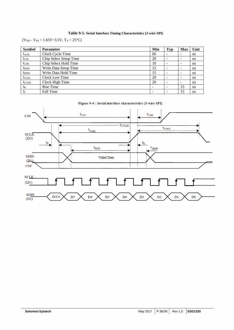
Table 9-5: Serial Interface Timing Characteristics (3-wire SPI)
(VDD - VSS = 1.65V~3.5V, TA = 25°C)
Symbol Parameter Min Typ Max Unit tcycle Clock Cycle Time 66 - - ns tCSS Chip Select Setup Time 20 - - ns tCSH Chip Select Hold Time 10 - - ns tDSW Write Data Setup Time 15 - - ns tDHW Write Data Hold Time 15 - - ns tCLKL Clock Low Time 20 - - ns tCLKH Clock High Time 20 - - ns tR Rise Time - - 15 ns tF Fall Time - - 15 ns
SSD1320 Rev 1.0 P 37/39 May 2017 Solomon Systech
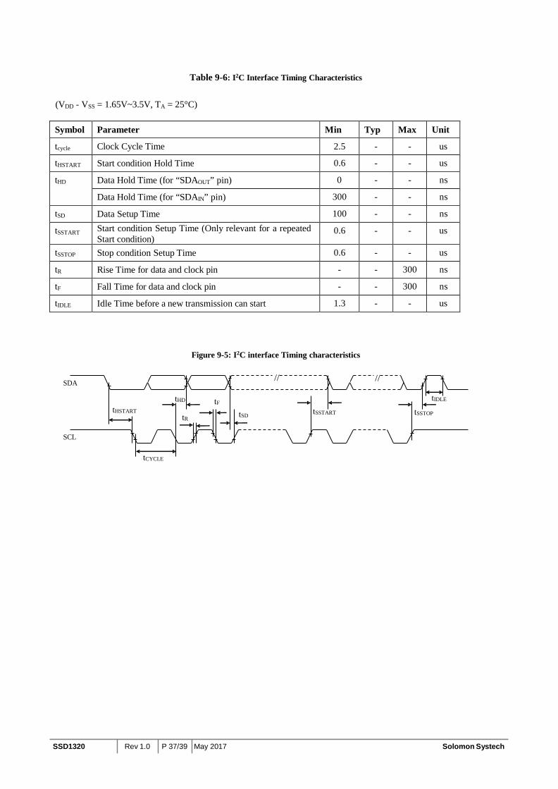
Figure 9-5: I2C interface Timing characteristics
SDA // //
tHD tF tHSTART
tR tSD tSSTART
tIDLE
tSSTOP
SCL
tCYCLE
Table 9-6: I2C Interface Timing Characteristics
(VDD - VSS = 1.65V~3.5V, TA = 25°C)
Symbol Parameter Min Typ Max Unit
tcycle Clock Cycle Time 2.5 - - us
tHSTART Start condition Hold Time 0.6 - - us
tHD Data Hold Time (for “SDAOUT” pin) 0 - - ns
Data Hold Time (for “SDAIN” pin) 300 - - ns
tSD Data Setup Time 100 - - ns
tSSTART Start condition Setup Time (Only relevant for a repeated Start condition)
0.6 - - us
tSSTOP Stop condition Setup Time 0.6 - - us
tR Rise Time for data and clock pin - - 300 ns
tF Fall Time for data and clock pin - - 300 ns
tIDLE Idle Time before a new transmission can start 1.3 - - us

Solomon Systech May 2017 P 38/39 Rev 1.0 SSD1320
10 APPLICATION EXAMPLE
Figure 10-1: Application Example of SSD1320Z
Note (1) The capacitor value is recommended value. Select appropriate value against module application. (2) Die gold bump face down. (3) All VLSS pads of the IC are recommended to be connected together to form a larger area of GND. (4) VLSS and VSS are not recommended to be connected on the ITO routing, but connected together in the PCB level at one common ground point for better grounding and noise insulation.
Pin connected to MCU interface: D[2:0], RES#, D/C#, CS# Pin internally connected to VLSS: VSL Pin internally connected to VSS (or VLL): D[7:3], BS[2:0], E, R/W#, CL, BGGND Pin internally connected to VDD (or VLL): CLS VBREF, VP, FR, T0, T1, TR[15:0], should be left open. C1, C2: 2.2uF (1)
C3: 1.0uF (1) place close to IC VDD and VSS pins on PCB Voltage at IREF = VCC – 2V. For VCC = 15V, IREF = 10uA: R1 = (Voltage at IREF - VSS) / IREF
≈ (15-2)V / 10uA ≈ 1.3MΩ
GND VDD SDA SCL D/C# RES# CS# VCC
C1
C3
R1 C2
VSS SSD1320Z VCC VCOMH IREF D2 D1 D0 D/C# RES# CS# VDD
VLSS
DISPLAY PANEL 160 x 160
The configuration for 4-wire SPI interface mode is shown in the following diagram: (VDD=1.8V, VCC =15V, IREF=10uA)
SEG
158
SEG
156
: : SEG
2 SE
G0
COM
0 CO
M1
. . . . . . . . . . . COM
158
COM
159
SEG
1 SE
G3
: : SEG
157

SSD1320 Rev 1.0 P 39/39 May 2017 Solomon Systech
The product(s) listed in this datasheet comply with Directive 2011/65/EU of the European Parliament and of the council of 8 June 2011 on the restriction of the use of certain hazardous substances in electrical and electronic equipment and People’s Republic of China Electronic Industry Standard GB/T 26572-2011 “Requirements for concentration limits for certain hazardous substances in electronic information products ( 电子电器产品
中限用物質的限用要求)”. Hazardous Substances test report is available upon request.
http://www.solomon-systech.com