solutions manual - guswnsla1223.tistory.comguswnsla1223.tistory.com/attachment/cfile29.uf@153... ·...
TRANSCRIPT

SOLUTIONS MANUAL
COMPUTER ORGANIZATION ANDARCHITECTURE
DESIGNING FOR PERFORMANCESEVENTH EDITION
WILLIAM STALLINGS
Copyright 2005: William Stallings

-2-
© 2005 by William Stallings
All rights reserved. No part of this document maybe reproduced, in any form or by any means, orposted on the Internet, without permission inwriting from the author.

-3-
NOTICE
This manual contains solutions to all of the review questions andhomework problems in Computer Organization and Architecture,Seventh Edition. If you spot an error in a solution or in the wording of aproblem, I would greatly appreciate it if you would forward theinformation via email to [email protected]. An errata sheet for this manual,if needed, is available at WilliamStallings.com
W.S.

-4-
TABLE OF CONTENTS
Chapter 2: Computer Evolution and Performance.....................................................5Chapter 3: Computer Function and Interconnection .................................................9Chapter 4: Cache Memory............................................................................................14Chapter 5: Internal Memory ........................................................................................27Chapter 6: External Memory........................................................................................33Chapter 7: Input/Output .............................................................................................37Chapter 8: Operating System Support .......................................................................43Chapter 9: Computer Arithmetic ................................................................................48Chapter 10: Instruction Sets: Characteristics and Functions.....................................61Chapter 11: Instruction Sets: Addressing Modes and Formats ................................72Chapter 12: Processor Structure and Function............................................................77Chapter 13: Reduced Instruction Set Computers (RISCs) .........................................83Chapter 14: Instruction-Level Parallelism and Superscalar Processors ..................87Chapter 15: The IA-64 Architecture..............................................................................93Chapter 16: Control Unit Operation .............................................................................97Chapter 17: Microprogrammed Control ....................................................................100Chapter 18: Parallel Processing ...................................................................................103Appendix A: Number Systems ......................................................................................112Appendix B: Digital Logic..............................................................................................113

-5-
AA NSWERS TO NSWERS TO QQ U E S T I O N SU E S T I O N S
2.1 In a stored program computer, programs are represented in a form suitable forstoring in memory alongside the data. The computer gets its instructions by readingthem from memory, and a program can be set or altered by setting the values of aportion of memory.
2.2 A main memory, which stores both data and instructions: an arithmetic and logicunit (ALU) capable of operating on binary data; a control unit, which interprets theinstructions in memory and causes them to be executed; and input and output(I/O) equipment operated by the control unit.
2.3 Gates, memory cells, and interconnections among gates and memory cells.
2.4 Moore observed that the number of transistors that could be put on a single chipwas doubling every year and correctly predicted that this pace would continue intothe near future.
2.5 Similar or identical instruction set: In many cases, the same set of machineinstructions is supported on all members of the family. Thus, a program thatexecutes on one machine will also execute on any other. Similar or identicaloperating system: The same basic operating system is available for all familymembers. Increasing speed: The rate of instruction execution increases in goingfrom lower to higher family members. Increasing Number of I/O ports: In goingfrom lower to higher family members. Increasing memory size: In going fromlower to higher family members. Increasing cost: In going from lower to higherfamily members.
2.6 In a microprocessor, all of the components of the CPU are on a single chip.
AA NSWERS TO NSWERS TO PP R O B L E M SR O B L E M S
2.1 This program is developed in [HAYE98]. The vectors A, B, and C are each stored in1,000 contiguous locations in memory, beginning at locations 1001, 2001, and 3001,respectively. The program begins with the left half of location 3. A countingvariable N is set to 999 and decremented after each step until it reaches –1. Thus,the vectors are processed from high location to low location.
CHAPTER 2COMPUTER EVOLUTION AND
PERFORMANCE

-6-
Location Instruction Comments0 999 Constant (count N)1 1 Constant2 1000 Constant3L LOAD M(2000) Transfer A(I) to AC3R ADD M(3000) Compute A(I) + B(I)4L STOR M(4000) Transfer sum to C(I)4R LOAD M(0) Load count N5L SUB M(1) Decrement N by 15R JUMP+ M(6, 20:39) Test N and branch to 6R if nonnegative6L JUMP M(6, 0:19) Halt6R STOR M(0) Update N7L ADD M(1) Increment AC by 17R ADD M(2)8L STOR M(3, 8:19) Modify address in 3L8R ADD M(2)9L STOR M(3, 28:39) Modify address in 3R9R ADD M(2)10L STOR M(4, 8:19) Modify address in 4L10R JUMP M(3, 0:19) Branch to 3L
2.2 a.Opcode Operand
00000001 000000000010
b. First, the CPU must make access memory to fetch the instruction. Theinstruction contains the address of the data we want to load. During the executephase accesses memory to load the data value located at that address for a totalof two trips to memory.
2.3 To read a value from memory, the CPU puts the address of the value it wants intothe MAR. The CPU then asserts the Read control line to memory and places theaddress on the address bus. Memory places the contents of the memory locationpassed on the data bus. This data is then transferred to the MBR. To write a value tomemory, the CPU puts the address of the value it wants to write into the MAR. TheCPU also places the data it wants to write into the MBR. The CPU then asserts theWrite control line to memory and places the address on the address bus and thedata on the data bus. Memory transfers the data on the data bus into thecorresponding memory location.

-7-
2.4Address Contents08A
08B
08C
08D
LOAD M(0FA)STOR M(0FB)LOAD M(0FA)JUMP +M(08D)LOAD –M(0FA)STOR M(0FB)
This program will store the absolute value of content at memory location 0FA intomemory location 0FB.
2.5 All data paths to/from MBR are 40 bits. All data paths to/from MAR are 12 bits.Paths to/from AC are 40 bits. Paths to/from MQ are 40 bits.
2.6 The purpose is to increase performance. When an address is presented to a memorymodule, there is some time delay before the read or write operation can beperformed. While this is happening, an address can be presented to the othermodule. For a series of requests for successive words, the maximum rate isdoubled.
2.7 The discrepancy can be explained by noting that other system components aside from clockspeed make a big difference in overall system speed. In particular, memory systems andadvances in I/O processing contribute to the performance ratio. A system is only as fast asits slowest link. In recent years, the bottlenecks have been the performance of memorymodules and bus speed.
2.8 As noted in the answer to Problem 2.7, even though the Intel machine may have afaster clock speed (2.4 GHz vs. 1.2 GHz), that does not necessarily mean the systemwill perform faster. Different systems are not comparable on clock speed. Otherfactors such as the system components (memory, buses, architecture) and theinstruction sets must also be taken into account. A more accurate measure is to runboth systems on a benchmark. Benchmark programs exist for certain tasks, such asrunning office applications, performing floating point operations, graphicsoperations, and so on. The systems can be compared to each other on how longthey take to complete these tasks. According to Apple Computer, the G4 iscomparable or better than a higher-clock speed Pentium on many benchmarks.
2.9 This representation is wasteful because to represent a single decimal digit from 0through 9 we need to have ten tubes. If we could have an arbitrary number of thesetubes ON at the same time, then those same tubes could be treated as binary bits.With ten bits, we can represent 210 patterns, or 1024 patterns. For integers, thesepatterns could be used to represent the numbers from 0 through 1023.

-8-
2.10Ic p m k τ
Instruction setarchitecture X X
Compiler technology X X XProcessorimplementation X X
Cache and memoryhierarchy X X
Source: [HWAN93]
2.11 MIPS rate = f/(CPI × 106)
2.12 a. We can express the MIPs rate as: [(MIPS rate)/106] = Ic/T. So that:Ic = T × [(MIPS rate)/106]. The ratio of the instruction count of the RS/6000 tothe VAX is [x × 18]/[12x × 1] = 1.5.
b. For the Vax, CPI = (5 MHz)/(1 MIPS) = 5.For the RS/6000, CPI = 25/18 = 1.39.
2.13 CPI = 1.55; MIPS rate = 25.8; Execution time = 3.87 ns. Source: [HWAN93]
2.14 a. Ultimately, the user is concerned with the execution time of a system, not itsexecution rate. If we take arithmetic mean of the MIPS rates of variousbenchmark programs, we get a result that is proportional to the sum of theinverses of execution times. But this is not inversely proportional to the sum ofexecution times. In other words, the arithmetic mean of the MIPS rate does notcleanly relate to execution time. On the other hand, the harmonic mean MIPSrate is the inverse of the average execution time.
b.Arithmetic mean Harmonic Mean Rank
Computer A 25.3 MIPS 0.25 MIPS 2Computer B 2.8 MIPS 0.21 MIPS 3Computer C 3.25 MIPS 2.1 MIPS 1

-9-
AA NSWERS TO NSWERS TO QQ U E S T I O N SU E S T I O N S
3.1 Processor-memory: Data may be transferred from processor to memory or frommemory to processor. Processor-I/O: Data may be transferred to or from aperipheral device by transferring between the processor and an I/O module. Dataprocessing: The processor may perform some arithmetic or logic operation on data.Control: An instruction may specify that the sequence of execution be altered.
3.2 Instruction address calculation (iac): Determine the address of the next instructionto be executed. Instruction fetch (if): Read instruction from its memory locationinto the processor. Instruction operation decoding (iod): Analyze instruction todetermine type of operation to be performed and operand(s) to be used. Operandaddress calculation (oac): If the operation involves reference to an operand inmemory or available via I/O, then determine the address of the operand. Operandfetch (of): Fetch the operand from memory or read it in from I/O. Data operation(do): Perform the operation indicated in the instruction. Operand store (os): Writethe result into memory or out to I/O.
3.3 (1) Disable all interrupts while an interrupt is being processed. (2) Define prioritiesfor interrupts and to allow an interrupt of higher priority to cause a lower-priorityinterrupt handler to be interrupted.
3.4 Memory to processor: The processor reads an instruction or a unit of data frommemory. Processor to memory: The processor writes a unit of data to memory. I/Oto processor: The processor reads data from an I/O device via an I/O module.Processor to I/O: The processor sends data to the I/O device. I/O to or frommemory: For these two cases, an I/O module is allowed to exchange data directlywith memory, without going through the processor, using direct memory access(DMA).
3.5 With multiple buses, there are fewer devices per bus. This (1) reduces propagationdelay, because each bus can be shorter, and (2) reduces bottleneck effects.
3.6 System pins: Include the clock and reset pins. Address and data pins: Include 32lines that are time multiplexed for addresses and data. Interface control pins:Control the timing of transactions and provide coordination among initiators andtargets. Arbitration pins: Unlike the other PCI signal lines, these are not sharedlines. Rather, each PCI master has its own pair of arbitration lines that connect itdirectly to the PCI bus arbiter. Error Reporting pins: Used to report parity andother errors. Interrupt Pins: These are provided for PCI devices that must generaterequests for service. Cache support pins: These pins are needed to support amemory on PCI that can be cached in the processor or another device. 64-bit Busextension pins: Include 32 lines that are time multiplexed for addresses and data
HAPTER 3COMPUTER FUNCTION AND
INTERCONNECTION
-10-
and that are combined with the mandatory address/data lines to form a 64-bitaddress/data bus. JTAG/Boundary Scan Pins: These signal lines support testingprocedures defined in IEEE Standard 1149.1.
AA NSWERS TO NSWERS TO PP R O B L E M SR O B L E M S
3.1 Memory (contents in hex): 300: 3005; 301: 5940; 302: 7006Step 1: 3005 → IR; Step 2: 3 → ACStep 3: 5940 → IR; Step 4: 3 + 2 = 5 → ACStep 5: 7006 → IR; Step 6: AC → Device 6
3.2 1. a. The PC contains 300, the address of the first instruction. This value is loadedin to the MAR.
b. The value in location 300 (which is the instruction with the value 1940 inhexadecimal) is loaded into the MBR, and the PC is incremented. These twosteps can be done in parallel.
c. The value in the MBR is loaded into the IR.2. a. The address portion of the IR (940) is loaded into the MAR.
b. The value in location 940 is loaded into the MBR.c. The value in the MBR is loaded into the AC.
3. a. The value in the PC (301) is loaded in to the MAR.b. The value in location 301 (which is the instruction with the value 5941) is
loaded into the MBR, and the PC is incremented.c. The value in the MBR is loaded into the IR.
4. a. The address portion of the IR (941) is loaded into the MAR.b. The value in location 941 is loaded into the MBR.c. The old value of the AC and the value of location MBR are added and the
result is stored in the AC.5. a. The value in the PC (302) is loaded in to the MAR.
b. The value in location 302 (which is the instruction with the value 2941) isloaded into the MBR, and the PC is incremented.
c. The value in the MBR is loaded into the IR.6. a. The address portion of the IR (941) is loaded into the MAR.
b. The value in the AC is loaded into the MBR.c. The value in the MBR is stored in location 941.
3.3 a. 224 = 16 MBytesb. (1) If the local address bus is 32 bits, the whole address can be transferred at
once and decoded in memory. However, because the data bus is only 16 bits, itwill require 2 cycles to fetch a 32-bit instruction or operand.(2) The 16 bits of the address placed on the address bus can't access the wholememory. Thus a more complex memory interface control is needed to latch thefirst part of the address and then the second part (because the microprocessorwill end in two steps). For a 32-bit address, one may assume the first half willdecode to access a "row" in memory, while the second half is sent later to accessa "column" in memory. In addition to the two-step address operation, themicroprocessor will need 2 cycles to fetch the 32 bit instruction/operand.
c. The program counter must be at least 24 bits. Typically, a 32-bit microprocessorwill have a 32-bit external address bus and a 32-bit program counter, unless on-chip segment registers are used that may work with a smaller program counter.If the instruction register is to contain the whole instruction, it will have to be
-11-
32-bits long; if it will contain only the op code (called the op code register) thenit will have to be 8 bits long.
3.4 In cases (a) and (b), the microprocessor will be able to access 216 = 64K bytes; theonly difference is that with an 8-bit memory each access will transfer a byte, whilewith a 16-bit memory an access may transfer a byte or a 16-byte word. For case (c),separate input and output instructions are needed, whose execution will generateseparate "I/O signals" (different from the "memory signals" generated with theexecution of memory-type instructions); at a minimum, one additional output pinwill be required to carry this new signal. For case (d), it can support 28 = 256 inputand 28 = 256 output byte ports and the same number of input and output 16-bitports; in either case, the distinction between an input and an output port is definedby the different signal that the executed input or output instruction generated.
3.5 Clock cycle =
18 MHz
= 125 ns
Bus cycle = 4 × 125 ns = 500 ns2 bytes transferred every 500 ns; thus transfer rate = 4 MBytes/sec
Doubling the frequency may mean adopting a new chip manufacturing technology(assuming each instructions will have the same number of clock cycles); doublingthe external data bus means wider (maybe newer) on-chip data bus drivers/latchesand modifications to the bus control logic. In the first case, the speed of the memorychips will also need to double (roughly) not to slow down the microprocessor; inthe second case, the "wordlength" of the memory will have to double to be able tosend/receive 32-bit quantities.
3.6 a. Input from the Teletype is stored in INPR. The INPR will only accept data fromthe Teletype when FGI=0. When data arrives, it is stored in INPR, and FGI isset to 1. The CPU periodically checks FGI. If FGI =1, the CPU transfers thecontents of INPR to the AC and sets FGI to 0.
When the CPU has data to send to the Teletype, it checks FGO. If FGO = 0,the CPU must wait. If FGO = 1, the CPU transfers the contents of the AC toOUTR and sets FGO to 0. The Teletype sets FGI to 1 after the word is printed.
b. The process described in (a) is very wasteful. The CPU, which is much fasterthan the Teletype, must repeatedly check FGI and FGO. If interrupts are used,the Teletype can issue an interrupt to the CPU whenever it is ready to accept orsend data. The IEN register can be set by the CPU (under programmer control)
3.7 a. During a single bus cycle, the 8-bit microprocessor transfers one byte while the16-bit microprocessor transfers two bytes. The 16-bit microprocessor has twicethe data transfer rate.
b. Suppose we do 100 transfers of operands and instructions, of which 50 are onebyte long and 50 are two bytes long. The 8-bit microprocessor takes 50 + (2 x50) = 150 bus cycles for the transfer. The 16-bit microprocessor requires 50 + 50= 100 bus cycles. Thus, the data transfer rates differ by a factor of 1.5. Source:[PROT88].
3.8 The whole point of the clock is to define event times on the bus; therefore, we wishfor a bus arbitration operation to be made each clock cycle. This requires that thepriority signal propagate the length of the daisy chain (Figure 3.26) in one clock

-12-
period. Thus, the maximum number of masters is determined by dividing theamount of time it takes a bus master to pass through the bus priority by the clockperiod.
3.9 The lowest-priority device is assigned priority 16. This device must defer to all theothers. However, it may transmit in any slot not reserved by the other SBI devices.
3.10 At the beginning of any slot, if none of the TR lines is asserted, only the priority 16device may transmit. This gives it the lowest average wait time under mostcircumstances. Only when there is heavy demand on the bus, which means thatmost of the time there is at least one pending request, will the priority 16 devicenot have the lowest average wait time.
3.11 a. With a clocking frequency of 10 MHz, the clock period is 10–9 s = 100 ns. Thelength of the memory read cycle is 300 ns.
b. The Read signal begins to fall at 75 ns from the beginning of the third clockcycle (middle of the second half of T3). Thus, memory must place the data onthe bus no later than 55 ns from the beginning of T3. Source: [PROT88]
3.12 a. The clock period is 125 ns. Therefore, two clock cycles need to be inserted.b. From Figure 3.19, the Read signal begins to rise early in T2. To insert two clock
cycles, the Ready line can be put in low at the beginning of T2 and kept low for250 ns. Source: [PROT88]
3.13 a. A 5 MHz clock corresponds to a clock period of 200 ns. Therefore, the Writesignal has a duration of 150 ns.
b. The data remain valid for 150 + 20 = 170 ns.c. One wait state. Source: [PROT88]
3.14 a. Without the wait states, the instruction takes 16 bus clock cycles. Theinstruction requires four memory accesses, resulting in 8 wait states. Theinstruction, with wait states, takes 24 clock cycles, for an increase of 50%.
b. In this case, the instruction takes 26 bus cycles without wait states and 34 buscycles with wait states, for an increase of 33%. Source: [PROT88]
3.15 a. The clock period is 125 ns. One bus read cycle takes 500 ns = 0.5 µs. If the buscycles repeat one after another, we can achieve a data transfer rate of 2 MB/s.
b. The wait state extends the bus read cycle by 125 ns, for a total duration of 0.625µs. The corresponding data transfer rate is 1/0.625 = 1.6 MB/s. Source:[PROT88]
3.16 A bus cycle takes 0.25 µs, so a memory cycle takes 1 µs. If both operands are even-aligned, it takes 2 µs to fetch the two operands. If one is odd-aligned, the timerequired is 3 µs. If both are odd-aligned, the time required is 4 µs. Source:[PROT88].
3.17 Consider a mix of 100 instructions and operands. On average, they consist of 20 32-bit items, 40 16-bit items, and 40 bytes. The number of bus cycles required for the16-bit microprocessor is (2 × 20) + 40 + 40 = 120. For the 32-bit microprocessor, thenumber required is 100. This amounts to an improvement of 20/120 or about 17%.Source: [PROT88].

-13-
3.18 The processor needs another nine clock cycles to complete the instruction. Thus,the Interrupt Acknowledge will start after 900 ns. Source: [PROT88].
3.19
Address
Bus Cmd
Address PhaseAddress PhaseAddress Phase Address Phase
Byte Enable Byte Enable Byte Enable
Data-1 Data-2 Data-3
CLK
1 2 3 4 5 6 7 8 9
FRAME#
AD
C/BE#
IRDY#
TRDY#
DEVSEL#
Wait State Wait State Wait State
Bus Transaction

-14-
AA NSWERS TO NSWERS TO QQ U E S T I O N SU E S T I O N S
4.1 Sequential access: Memory is organized into units of data, called records. Accessmust be made in a specific linear sequence. Direct access: Individual blocks orrecords have a unique address based on physical location. Access is accomplishedby direct access to reach a general vicinity plus sequential searching, counting, orwaiting to reach the final location. Random access: Each addressable location inmemory has a unique, physically wired-in addressing mechanism. The time toaccess a given location is independent of the sequence of prior accesses and isconstant.
4.2 Faster access time, greater cost per bit; greater capacity, smaller cost per bit; greatercapacity, slower access time.
4.3 It is possible to organize data across a memory hierarchy such that the percentageof accesses to each successively lower level is substantially less than that of the levelabove. Because memory references tend to cluster, the data in the higher-levelmemory need not change very often to satisfy memory access requests.
4.4 In a cache system, direct mapping maps each block of main memory into only onepossible cache line. Associative mapping permits each main memory block to beloaded into any line of the cache. In set-associative mapping, the cache is dividedinto a number of sets of cache lines; each main memory block can be mapped intoany line in a particular set.
4.5 One field identifies a unique word or byte within a block of main memory. Theremaining two fields specify one of the blocks of main memory. These two fieldsare a line field, which identifies one of the lines of the cache, and a tag field, whichidentifies one of the blocks that can fit into that line.
4.6 A tag field uniquely identifies a block of main memory. A word field identifies aunique word or byte within a block of main memory.
4.7 One field identifies a unique word or byte within a block of main memory. Theremaining two fields specify one of the blocks of main memory. These two fieldsare a set field, which identifies one of the sets of the cache, and a tag field, whichidentifies one of the blocks that can fit into that set.
4.8 Spatial locality refers to the tendency of execution to involve a number of memorylocations that are clustered. Temporal locality refers to the tendency for a processorto access memory locations that have been used recently.
4.9 Spatial locality is generally exploited by using larger cache blocks and byincorporating prefetching mechanisms (fetching items of anticipated use) into the
CHAPTER 4CACHE MEMORY

-15-
cache control logic. Temporal locality is exploited by keeping recently usedinstruction and data values in cache memory and by exploiting a cache hierarchy.
AA NSWERS TO NSWERS TO PP R O B L E M SR O B L E M S
4.1 The cache is divided into 16 sets of 4 lines each. Therefore, 4 bits are needed toidentify the set number. Main memory consists of 4K = 212 blocks. Therefore, the setplus tag lengths must be 12 bits and therefore the tag length is 8 bits. Each blockcontains 128 words. Therefore, 7 bits are needed to specify the word.
TAG SET WORDMain memory address = 8 4 7
4.2 There are a total of 8 kbytes/16 bytes = 512 lines in the cache. Thus the cacheconsists of 256 sets of 2 lines each. Therefore 8 bits are needed to identify the setnumber. For the 64-Mbyte main memory, a 26-bit address is needed. Main memoryconsists of 64-Mbyte/16 bytes = 222 blocks. Therefore, the set plus tag lengths mustbe 22 bits, so the tag length is 14 bits and the word field length is 4 bits.
TAG SET WORDMain memory address = 14 8 4
4.3Address 111111 666666 BBBBBB
a. Tag/Line/Word 11/444/1 66/1999/2 BB/2EEE/3b. Tag /Word 44444/1 199999/2 2EEEEE/3c. Tag/Set/Word 22/444/1 CC/1999/2 177/EEE/3
4.4 a. Address length: 24; number of addressable units: 224; block size: 4; number ofblocks in main memory: 222; number of lines in cache: 214; size of tag: 8.
b. Address length: 24; number of addressable units: 224; block size: 4; number ofblocks in main memory: 222; number of lines in cache: 4000 hex; size of tag: 22.
c. Address length: 24; number of addressable units: 224; block size: 4; number ofblocks in main memory: 222; number of lines in set: 2; number of sets: 213;number of lines in cache: 214; size of tag: 9.
4.5 Block frame size = 16 bytes = 4 doublewordsNumber of block frames in cache =
16 KBytes16 Bytes
= 1024
Number of sets = Number of block frames
Associativity=
10244
= 256 sets
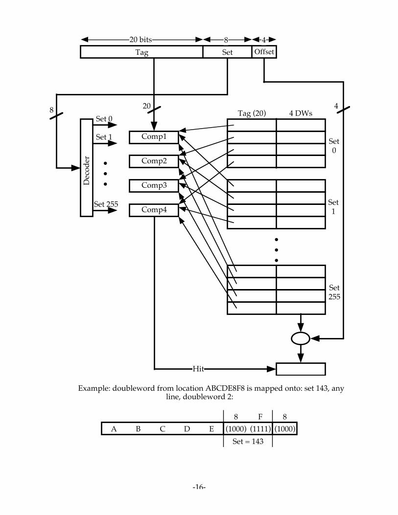
-16-
.
OffsetSetTag20 bits 8 4
Dec
oder
Comp1
Comp2
Comp3
Comp4
8 20Set 0
Set 1
Set 255
•••
•••
Set0
Set1
Set255
Tag (20) 4 DWs
Hit
4
Example: doubleword from location ABCDE8F8 is mapped onto: set 143, anyline, doubleword 2:
(1000)A B C D E (1111) (1000)8 F 8
Set = 143

-17-
4.6
12 bits 10 bits
4.7 A 32-bit address consists of a 21-bit tag field, a 7-bit set field, and a 4-bit word field.Each set in the cache includes 3 LRU bits and four lines. Each line consists of 4 32-bit words, a valid bit, and a 21-bit tag.
4.8 a. 8 leftmost bits = tag; 5 middle bits = line number; 3 rightmost bits = bytenumber
b. slot 3; slot 6; slot 3; slot 21c. Bytes with addresses 0001 1010 0001 1000 through 0001 1010 0001 1111 are
stored in the cached. 256 bytese. Because two items with two different memory addresses can be stored in the
same place in the cache. The tag is used to distinguish between them.

-18-
4.9 a. The bits are set according to the following rules with each access to the set:
1. If the access is to L0 or L1, B0 ← 1.2. If the access is to L0, B1 ← 1.3. If the access is to L1, B1 ← 0.4. If the access is to L2 or L3, B0 ← 0.5. If the access is to L2, B2 ← 1.6. If the access is to L3, B2 ← 0.
The replacement algorithm works as follows (Figure 4.15): When a line must bereplaced, the cache will first determine whether the most recent use was fromL0 and L1 or L2 and L3. Then the cache will determine which of the pair ofblocks was least recently used and mark it for replacement. When the cache isinitialized or flushed all 128 sets of three LRU bits are set to zero.
b. The 80486 divides the four lines in a set into two pairs (L0, L1 and L2, L3). BitB0 is used to select the pair that has been least-recently used. Within each pair,one bit is used to determine which member of the pair was least-recently used.However, the ultimate selection only approximates LRU. Consider the case inwhich the order of use was: L0, L2, L3, L1. The least-recently used pair is (L2,L3) and the least-recently used member of that pair is L2, which is selected forreplacement. However, the least-recently used line of all is L0. Depending onthe access history, the algorithm will always pick the least-recently used entryor the second least-recently used entry.
c. The most straightforward way to implement true LRU for a four-line set is toassociate a two bit counter with each line. When an access occurs, the counterfor that block is set to 0; all counters with values lower than the original valuefor the accessed block are incremented by 1. When a miss occurs and the set isnot full, a new block is brought in, its counter is set to 0 and all other countersare incremented by 1. When a miss occurs and the set is full, the block withcounter value 3 is replaced; its counter is set to 0 and all other counters areincremented by 1. This approach requires a total of 8 bits.
In general, for a set of N blocks, the above approach requires 2N bits. Amore efficient scheme can be designed which requires only N(N–1)/2 bits. Thescheme operates as follows. Consider a matrix R with N rows and N columns,and take the upper-right triangular portion of the matrix, not counting thediagonal. For N = 4, we have the following layout:
R(1,2) R(1,3) R(1,4)R(2,3) R(2,4)
R(3,4)
When line I is referenced, row I of R(I,J) is set to 1, and column I of R(J,I) is setto 0. The LRU block is the one for which the row is entirely equal to 0 (for thosebits in the row; the row may be empty) and for which the column is entirely 1(for all the bits in the column; the column may be empty). As can be seen for N= 4, a total of 6 bits are required.

-19-
4.10 Block size = 4 words = 2 doublewords; associativity K = 2; cache size = 4048words; C = 1024 block frames; number of sets S = C/K = 512; main memory = 64K× 32 bits = 256 Kbytes = 218 bytes; address = 18 bits..
Tag Set
Word bits
(6 bits) (9) (2) (1)
Compare0
Compare1
Dec
oder
Set 0
Set 511
•••
Tag (6) 4 wordsSet 0(8 words)
Set 511(8 words)
•••
word select
4.11 a. Address format: Tag = 20 bits; Line = 6 bits; Word = 6 bitsNumber of addressable units = 2s+w = 232 bytes; number of blocks in mainmemory = 2s = 226; number of lines in cache 2r = 26 = 64; size of tag = 20 bits.
b. Address format: Tag = 26 bits; Word = 6 bitsNumber of addressable units = 2s+w = 232 bytes; number of blocks in mainmemory = 2s = 226; number of lines in cache = undetermined; size of tag = 26bits.
c. Address format: Tag = 9 bits; Set = 17 bits; Word = 6 bitsNumber of addressable units = 2s+w = 232 bytes; Number of blocks in mainmemory = 2s = 226; Number of lines in set = k = 4; Number of sets in cache = 2d
= 217; Number of lines in cache = k × 2d =219; Size of tag = 9 bits.
4.12 a. Because the block size is 16 bytes and the word size is 1 byte, this means thereare 16 words per block. We will need 4 bits to indicate which word we wantout of a block. Each cache line/slot matches a memory block. That means eachcache slot contains 16 bytes. If the cache is 64Kbytes then 64Kbytes/16 = 4096cache slots. To address these 4096 cache slots, we need 12 bits (212 = 4096).Consequently, given a 20 bit (1 MByte) main memory address:
Bits 0-3 indicate the word offset (4 bits)Bits 4-15 indicate the cache slot (12 bits)Bits 16-19 indicate the tag (remaining bits)
F0010 = 1111 0000 0000 0001 0000Word offset = 0000 = 0Slot = 0000 0000 0001 = 001Tag = 1111 = F
01234 = 0000 0001 0010 0011 0100Word offset = 0100 = 4Slot = 0001 0010 0011 = 123Tag = 0000 = 0

-20-
CABBE = 1100 1010 1011 1011 1110Word offset = 1110 = ESlot = 1010 1011 1011 = ABBTag = 1100 = C
b. We need to pick any address where the slot is the same, but the tag (andoptionally, the word offset) is different. Here are two examples where the slotis 1111 1111 1111Address 1:
Word offset = 1111Slot = 1111 1111 1111Tag = 0000Address = 0FFFF
Address 2:Word offset = 0001Slot = 1111 1111 1111Tag = 0011Address = 3FFF1
c. With a fully associative cache, the cache is split up into a TAG and aWORDOFFSET field. We no longer need to identify which slot a memory blockmight map to, because a block can be in any slot and we will search each cacheslot in parallel. The word-offset must be 4 bits to address each individual wordin the 16-word block. This leaves 16 bits leftover for the tag.F0010
Word offset = 0hTag = F001h
CABBEWord offset = EhTag = CABBh
d. As computed in part a, we have 4096 cache slots. If we implement a two -wayset associative cache, then it means that we put two cache slots into one set.Our cache now holds 4096/2 = 2048 sets, where each set has two slots. Toaddress these 2048 sets we need 11 bits (211 = 2048). Once we address a set, wewill simultaneously search both cache slots to see if one has a tag that matchesthe target. Our 20-bit address is now broken up as follows:
Bits 0-3 indicate the word offsetBits 4-14 indicate the cache setBits 15-20 indicate the tag
F0010 = 1111 0000 0000 0001 0000Word offset = 0000 = 0Cache Set = 000 0000 0001 = 001Tag = 11110 = 1 1110 = 1E
CABBE = 1100 1010 1011 1011 1110Word offset = 1110 = ECache Set = 010 1011 1011 = 2BBTag = 11001 = 1 1001 = 19
4.13 Associate a 2-bit counter with each of the four blocks in a set. Initially, arbitrarilyset the four values to 0, 1, 2, and 3 respectively. When a hit occurs, the counter ofthe block that is referenced is set to 0. The other counters in the set with valuesoriginally lower than the referenced counter are incremented by 1; the remainingcounters are unchanged. When a miss occurs, the block in the set whose counter

-21-
value is 3 is replaced and its counter set to 0. All other counters in the set areincremented by 1.
4.14 Writing back a line takes 30 + (7 × 5) = 65 ns, enough time for 2.17 single-wordmemory operations. If the average line that is written at least once is written morethan 2.17 times, the write-back cache will be more efficient.
4.15 a. A reference to the first instruction is immediately followed by a reference to thesecond.
b. The ten accesses to a[i] within the inner for loop which occur within a shortinterval of time.
4.16 DefineCi = Average cost per bit, memory level iSi = Size of memory level iTi = Time to access a word in memory level iHi = Probability that a word is in memory i and in no higher-level memoryBi = Time to transfer a block of data from memory level (i + 1) to memory level i
Let cache be memory level 1; main memory, memory level 2; and so on, for a totalof N levels of memory. Then
Cs =
CiSii=1
N∑
Sii=1
N∑
The derivation of Ts is more complicated. We begin with the result fromprobability theory that:
Expected Value of x = i Pr x = 1[ ]
i=1
N∑
We can write:
Ts = TiHi
i=1
N∑
We need to realize that if a word is in M1 (cache), it is read immediately. If it is inM2 but not M1, then a block of data is transferred from M2 to M1 and then read.Thus:
T2 = B1 + T1
Further
T3 = B2 + T2 = B1 + B2 + T1

-22-
Generalizing:
Ti = Bj + T1
j=1
i−1∑
So
Ts = BjHi( )
j=1
i−1∑
i=2
N∑ + T1 Hi
i=1
N∑
But
Hii=1
N∑ = 1
Finally
Ts = BjHi( )
j=1
i−1∑
i=2
N∑ + T1
4.17 Main memory consists of 512 blocks of 64 words. Cache consists of 16 sets; each setconsists of 4 slots; each slot consists of 64 words. Locations 0 through 4351 in mainmemory occupy blocks 0 through 67. On the first fetch sequence, block 0 through15 are read into sets 0 through 15; blocks 16 through 31 are read into sets 0 through15; blocks 32-47 are read into sets 0 through 15; blocks 48-63 are read into sets 0through 15; and blocks 64-67 are read into sets 0 through 3. Because each set has 4slots, there is no replacement needed through block 63. The last 4 groups of blocksinvolve a replacement. On each successive pass, replacements will be required insets 0 through 3, but all of the blocks in sets 4 through 15 remain undisturbed.Thus, on each successive pass, 48 blocks are undisturbed, and the remaining 20must read in.
Let T be the time to read 64 words from cache. Then 10T is the time to read 64words from main memory. If a word is not in the cache, then it can only be readyby first transferring the word from main memory to the cache and then reading thecache. Thus the time to read a 64-word block from cache if it is missing is 11T.
We can now express the improvement factor as follows. With no cache
Fetch time = (10 passes) (68 blocks/pass) (10T/block) = 6800T
With cache
Fetch time = (68) (11T) first pass+ (9) (48) (T) + (9) (20) (11T) other passes
= 3160T
Improvement = 6800T3160T = 2.15
4.18 a. Access 63 1 Miss Block 3 → Slot 3Access 64 1 Miss Block 4 → Slot 0Access 65-70 6 Hits

-23-
Access 15 1 Miss Block 0 → Slot 0 First LoopAccess 16 1 Miss Block 1 → Slot 1Access 17-31 15 HitsAccess 32 1 Miss Block 2 → Slot 2Access 80 1 Miss Block 5 → Slot 1Access 81-95 15 HitsAccess 15 1 Hit Second LoopAccess 16 1 Miss Block 1 → Slot 1Access 17-31 15 hitsAccess 32 1 HitAccess 80 1 Miss Block 5 → Slot 1Access 81-95 15 hitsAccess 15 1 Hit Third LoopAccess 16 1 Miss Block 1 → Slot 1Access 17-31 15 hitsAccess 32 1 HitAccess 80 1 Miss Block 5 → Slot 1Access 81-95 15 hitsAccess 15 1 Hit Fourth Loop… Pattern continues to the Tenth Loop
For lines 63-70 2 Misses 6 HitsFirst loop 15-32, 80-95 4 Misses 30 HitsSecond loop 15-32, 80-95 2 Misses 32 HitsThird loop 15-32, 80-95 2 Misses 32 HitsFourth loop 15-32, 80-95 2 Misses 32 HitsFifth loop 15-32, 80-95 2 Misses 32 HitsSixth loop 15-32, 80-95 2 Misses 32 HitsSeventh loop 15-32, 80-95 2 Misses 32 HitsEighth loop 15-32, 80-95 2 Misses 32 HitsNinth loop 15-32, 80-95 2 Misses 32 HitsTenth loop 15-32, 80-95 2 Misses 32 HitsTotal: 24 Misses 324 HitsHit Ratio = 324/348 = 0.931
b. Access 63 1 Miss Block 3 → Set 1 Slot 2Access 64 1 Miss Block 4 → Set 0 Slot 0Access 65-70 6 HitsAccess 15 1 Miss Block 0 → Set 0 Slot 1 First LoopAccess 16 1 Miss Block 1 → Set 1 Slot 3Access 17-31 15 HitsAccess 32 1 Miss Block 2 → Set 0 Slot 0Access 80 1 Miss Block 5 → Set 1 Slot 2Access 81-95 15 HitsAccess 15 1 Hit Second LoopAccess 16-31 16 HitsAccess 32 1 HitAccess 80-95 16 Hits… All hits for the next eight iterations
For lines 63-70 2 Misses 6 HitsFirst loop 15-32, 80-95 4 Misses 30 Hits

-24-
Second loop 15-32, 80-95 0 Misses 34 HitsThird loop 15-32, 80-95 0 Misses 34 HitsFourth loop 15-32, 80-95 0 Misses 34 HitsFifth loop 15-32, 80-95 0 Misses 34 HitsSixth loop 15-32, 80-95 0 Misses 34 HitsSeventh loop 15-32, 80-95 0 Misses 34 HitsEighth loop 15-32, 80-95 0 Misses 34 HitsNinth loop 15-32, 80-95 0 Misses 34 HitsTenth loop 15-32, 80-95 0 Misses 34 HitsTotal = 6 Misses 342 HitsHit Ratio = 342/348 = 0.983
4.19 a. Cost = Cm × 8 × 106 = 8 × 10³ ¢ = $80b. Cost = Cc × 8 × 106 = 8 × 10⁴ ¢ = $800c. From Equation (4.1) : 1.1 × T1 = T1 + (1 – H)T2
(0.1)(100) = (1 – H)(1200)H = 1190/1200
4.20 a. Under the initial conditions, using Equation (4.1), the average access time is
T1 + (1 - H) T2 = 1 + (0.05) T2
Under the changed conditions, the average access time is
1.5 + (0.03) T2
For improved performance, we must have
1 + (0.05) T2 > 1.5 + (0.03) T2
Solving for T2, the condition is T2 > 50b. As the time for access when there is a cache miss become larger, it becomes
more important to increase the hit ratio.
4.21 a. First, 2.5 ns are needed to determine that a cache miss occurs. Then, therequired line is read into the cache. Then an additional 2.5 ns are needed toread the requested word.
Tmiss = 2.5 + 50 + (15)(5) + 2.5 = 130 nsb. The value Tmiss from part (a) is equivalent to the quantity (T1 + T2) in Equation
(4.1). Under the initial conditions, using Equation (4.1), the average access timeis
Ts = H × T1 + (1 – H) × (T1 + T2) = (0.95)(2.5) + (0.05)(130) = 8.875 ns
Under the revised scheme, we have:Tmiss = 2.5 + 50 + (31)(5) + 2.5 = 210 ns
and
Ts = H × T1 + (1 – H) × (T1 + T2) = (0.97)(2.5) + (0.03)(210) = 8.725 ns

-25-
4.22 There are three cases to consider:
Location of referenced word Probability Total time for access in nsIn cache 0.9 20Not in cache, but in mainmemory
(0.1)(0.6) = 0.06 60 + 20 = 80
Not in cache or main memory (0.1)(0.4) = 0.04 12ms + 60 + 20 = 12,000,080
So the average access time would be:
Avg = (0.9)(20) + (0.06)(80) + (0.04)(12000080) = 480026 ns
4.23 a. Consider the execution of 100 instructions. Under write-through, this creates200 cache references (168 read references and 32 write references). On average,the read references result in (0.03) × 168 = 5.04 read misses. For each read miss,a line of memory must be read in, generating 5.04 × 8 = 40.32 physical words oftraffic. For write misses, a single word is written back, generating 32 words oftraffic. Total traffic: 72.32 words. For write back, 100 instructions create 200cache references and thus 6 cache misses. Assuming 30% of lines are dirty, onaverage 1.8 of these misses require a line write before a line read. Thus, totaltraffic is (6 + 1.8) × 8 = 62.4 words. The traffic rate:Write through = 0.7232 byte/instructionWrite back = 0.624 bytes/instruction
b. For write-through: [(0.05) × 168 × 8] + 32 = 99.2 → 0.992 bytes/instructionFor write-back: (10 + 3) × 8 = 104 → 0.104 bytes/instruction
c. For write-through: [(0.07) × 168 × 8] + 32 = 126.08 → 0.12608 bytes/instructionFor write-back: (14 + 4.2) × 8 = 145.6 → 0.1456 bytes/instruction
d. A 5% miss rate is roughly a crossover point. At that rate, the memory traffic isabout equal for the two strategies. For a lower miss rate, write-back is superior.For a higher miss rate, write-through is superior.
4.24 a. One clock cycle equals 60 ns, so a cache access takes 120 ns and a main memoryaccess takes 180 ns. The effective length of a memory cycle is (0.9 × 120) + (0.1 ×180) = 126 ns.
b. The calculation is now (0.9 × 120) + (0.1 × 300) = 138 ns. Clearly theperformance degrades. However, note that although the memory access timeincreases by 120 ns, the average access time increases by only 12 ns. Source:[PROT88].
4.25 a. For a 1 MIPS processor, the average instruction takes 1000 ns to fetch andexecute. On average, an instruction uses two bus cycles for a total of 600 ns, sothe bus utilization is 0.6
b. For only half of the instructions must the bus be used for instruction fetch. Busutilization is now (150 + 300)/1000 = 0.45. This reduces the waiting time forother bus requestors, such as DMA devices and other microprocessors.
4.26 a. Ta = Tc + (1 – H)Tb + W(Tm – Tc)b. Ta = Tc + (1 – H)Tb + Wb(1 – H)Tb = Tc + (1 – H)(1 + Wb)Tb

-26-
4.27 Ta = [Tc1 + (1 – H1)Tc2] + (1 – H2)Tm
4.28 a. miss penalty = 1 + 4 = 5 clock cyclesb. miss penalty = 4 × (1 + 4 ) = 20 clock cyclesc. miss penalty = miss penalty for one word + 3 = 8 clock cycles.
4.29 The average miss penalty equals the miss penalty times the miss rate. For a linesize of one word, average miss penalty = 0.032 x 5 = 0.16 clock cycles. For a linesize of 4 words and the nonburst transfer, average miss penalty = 0.011 x 20 = 0.22clock cycles. For a line size of 4 words and the burst transfer, average miss penalty= 0.011 x 8 = 0.132 clock cycles.

-27-
AA NSWERS TO NSWERS TO QQ U E S T I O N SU E S T I O N S
5.1 They exhibit two stable (or semistable) states, which can be used to represent binary1 and 0; they are capable of being written into (at least once), to set the state; theyare capable of being read to sense the state.
5.2 (1) A memory in which individual words of memory are directly accessed throughwired-in addressing logic. (2) Semiconductor main memory in which it is possibleboth to read data from the memory and to write new data into the memory easilyand rapidly.
5.3 SRAM is used for cache memory (both on and off chip), and DRAM is used formain memory.
5.4 SRAMs generally have faster access times than DRAMs. DRAMS are less expensiveand smaller than SRAMs.
5.5 A DRAM cell is essentially an analog device using a capacitor; the capacitor canstore any charge value within a range; a threshold value determines whether thecharge is interpreted as 1 or 0. A SRAM cell is a digital device, in which binaryvalues are stored using traditional flip-flop logic-gate configurations.
5.6 Microprogrammed control unit memory; library subroutines for frequently wantedfunctions; system programs; function tables.
5.7 EPROM is read and written electrically; before a write operation, all the storagecells must be erased to the same initial state by exposure of the packaged chip toultraviolet radiation. Erasure is performed by shining an intense ultraviolet lightthrough a window that is designed into the memory chip. EEPROM is a read-mostly memory that can be written into at any time without erasing prior contents;only the byte or bytes addressed are updated. Flash memory is intermediatebetween EPROM and EEPROM in both cost and functionality. Like EEPROM, flashmemory uses an electrical erasing technology. An entire flash memory can beerased in one or a few seconds, which is much faster than EPROM. In addition, it ispossible to erase just blocks of memory rather than an entire chip. However, flashmemory does not provide byte-level erasure. Like EPROM, flash memory uses onlyone transistor per bit, and so achieves the high density (compared with EEPROM)of EPROM.
5.8 A0 - A1 = address lines:. CAS = column address select:. D1 - D4 = data lines. NC: =no connect. OE: output enable. RAS = row address select:. Vcc: = voltage source.Vss: = ground. WE: write enable.
5.9 A bit appended to an array of binary digits to make the sum of all the binary digits,including the parity bit, always odd (odd parity) or always even (even parity).
CHAPTER 5INTERNAL MEMORY

-28-
5.10 A syndrome is created by the XOR of the code in a word with a calculated versionof that code. Each bit of the syndrome is 0 or 1 according to if there is or is not amatch in that bit position for the two inputs. If the syndrome contains all 0s, noerror has been detected. If the syndrome contains one and only one bit set to 1,then an error has occurred in one of the 4 check bits. No correction is needed. If thesyndrome contains more than one bit set to 1, then the numerical value of thesyndrome indicates the position of the data bit in error. This data bit is inverted forcorrection.
5.11 Unlike the traditional DRAM, which is asynchronous, the SDRAM exchanges datawith the processor synchronized to an external clock signal and running at the fullspeed of the processor/memory bus without imposing wait states.
AA NSWERS TO NSWERS TO PP R O B L E M SR O B L E M S
5.1 The 1-bit-per-chip organization has several advantages. It requires fewer pins onthe package (only one data out line); therefore, a higher density of bits can beachieved for a given size package. Also, it is somewhat more reliable because it hasonly one output driver. These benefits have led to the traditional use of 1-bit-per-chip for RAM. In most cases, ROMs are much smaller than RAMs and it is oftenpossible to get an entire ROM on one or two chips if a multiple-bits-per-chiporganization is used. This saves on cost and is sufficient reason to adopt thatorganization.
5.2 In 1 ms, the time devoted to refresh is 64 × 150 ns = 9600 ns. The fraction of timedevoted to memory refresh is (9.6 × 10⁻⁶ s)/10–3 s = 0.0096, which is approximately1%.
5.3 a. Memory cycle time = 60 + 40 = 100 ns. The maximum data rate is 1 bit every 100ns, which is 10 Mbps.
b. 320 Mbps = 40 MB/s.

-29-
5.4
S0 S1
S2S3
S4S5
S6S7
A0
A19
A20A21A22
Decoder
Chip select
1 Mb
Chip select
1 Mb
Chip select
1 Mb
Chip select
1 Mb
Chip select
1 Mb
Chip select
1 Mb
Chip select
1 Mb
Chip select
1 Mb•••
5.5 a. The length of a clock cycle is 100 ns. Mark the beginning of T1 as time 0.AddressEnable returns to a low at 75.
€
RAS goes active 50 ns later, or time 125. Datamust become available by the DRAMs at time 300 – 60 = 240. Hence, access timemust be no more than 240 – 125 = 115 ns.
b. A single wait state will increase the access time requirement to 115 + 100 = 215ns. This can easily be met by DRAMs with access times of 150 ns. Source:[PROT88].
5.6 a. The refresh period from row to row must be no greater than4000/256 = 15.625 µs.
b. An 8-bit counter is needed to count 256 rows (28 = 256). Source: [PROT88].
5.7 a.pulse a = writepulse b = writepulse c = writepulse d = writepulse e= write
pulse f = writepulse g = store-disable outputspulse h = readpulse i = readpulse j = read
pulse k = readpulse l = readpulse m = readpulse n = store-disable outputs

-30-
b. Data is read in via pins (D3, D2, D1, D0)word 0 = 1111 (written into location 0 during pulse a)word 1 = 1110 (written into location 0 during pulse b)word 2 = 1101 (written into location 0 during pulse c)word 3 = 1100 (written into location 0 during pulse d)word 4 = 1011 (written into location 0 during pulse e)word 5 = 1010 (written into location 0 during pulse f)word 6 = random (did not write into this location 0)
c. Output leads are (O3, O2, O1, O0)pulse h: 1111 (read location 0)pulse i: 1110 (read location 1)pulse j: 1101 (read location 2)pulse k: 1100 (read location 3)pulse l: 1011 (read location 4)pulse m: 1010 (read location 5)
5.8 8192/64 = 128 chips; arranged in 8 rows by 64 columns:
.
• • •
• • •
•••
•••
•••
0 1 7
112 113 119
Section 0 (even)• • •
• • •
•••
•••
•••
8 9 15
120 121 127
Section 1 (odd)
A0 = L A0 = H
Dec
oder
Row 0Row 1
Row 7
•••
8RowsAll zeros
Ak-A10 A9-A7
3A6-A1
6
AB
En
8
8Depends on
type ofprocessor
5.9 Total memory is 1 megabyte = 8 megabits. It will take 32 DRAMs to construct thememory (32 × 256 Kb = 8 Mb). The composite failure rate is 2000 × 32 = 64,000 FITS.From this, we get a MTBF = 109/64,000 = 15625 hours = 22 months. Source:[PROT88].
5.10 The stored word is 001101001111, as shown in Figure 5.10. Now suppose that theonly error is in C8, so that the fetched word is 001111001111. Then the receivedblock results in the following table:
Position 12 11 10 9 8 7 6 5 4 3 2 1Bits D8 D7 D6 D5 C8 D4 D3 D2 C4 D1 C2 C1Block 0 0 1 1 1 1 0 0 1 1 1 1Codes 1010 1001 0111 0011

-31-
The check bit calculation after reception:
Position CodeHamming 1111
10 10109 10017 01113 0011
XOR = syndrome 1000
The nonzero result detects and error and indicates that the error is in bit position 8,which is check bit C8.
5.11 Data bits with value 1 are in bit positions 12, 11, 5, 4, 2, and 1:
Position 12 11 10 9 8 7 6 5 4 3 2 1Bits D8 D7 D6 D5 C8 D4 D3 D2 C4 D1 C2 C1Block 1 1 0 0 0 0 1 0Codes 1100 1011 0101
The check bits are in bit numbers 8, 4, 2, and 1.Check bit 8 calculated by values in bit numbers: 12, 11, 10 and 9Check bit 4 calculated by values in bit numbers: 12, 7, 6, and 5Check bit 2 calculated by values in bit numbers: 11, 10, 7, 6 and 3Check bit 1 calculated by values in bit numbers: 11, 9, 7, 5 and 3Thus, the check bits are: 0 0 1 0
5.12 The Hamming Word initially calculated was:
bit number: 12 11 10 9 8 7 6 5 4 3 2 10 0 1 1 0 1 0 0 1 1 1 1
Doing an exclusive-OR of 0111 and 1101 yields 1010 indicating an error in bit 10 ofthe Hamming Word. Thus, the data word read from memory was 00011001.
5.13 Need K check bits such that 1024 + K ≤ 2K – 1.The minimum value of K that satisfies this condition is 11.

-32-
5.14 As Table 5.2 indicates, 5 check bits are needed for an SEC code for 16-bit datawords. The layout of data bits and check bits:
Bit Position Position Number Check Bits Data Bits21 10101 M1620 10100 M1519 10011 M1418 10010 M1317 10001 M1216 10000 C1615 01111 M1114 01110 M1013 01101 M912 01100 M811 01011 M710 01010 M6 9 01001 M5 8 01000 C8 7 00111 M4 6 00110 M3 5 00101 M2 4 00100 C4 3 00011 M1 2 00010 C2 1 00001 C1
The equations are calculated as before, for example,C1= M1 ⊕ M2 ⊕ M4 ⊕ M5 ⊕ M7 ⊕ M9 ⊕ M11 ⊕ M12 ⊕ M14 ⊕ M16.
For the word 0101000000111001, the code isC16 = 1; C8 = 1; C 4 = 1; C2 = 1; C1 = 0.
If an error occurs in data bit 4:C16 = 1 ; C8 =1; C4 = 0; C2 = 0; C1 = 1.
Comparing the two:
C16 C8 C4 C2 C11 1 1 1 01 1 0 0 10 0 1 1 1
The result is an error identified in bit position 7, which is data bit 4.

-33-
AA NSWERS TO NSWERS TO QQ U E S T I O N SU E S T I O N S
6.1 Improvement in the uniformity of the magnetic film surface to increase diskreliability. A significant reduction in overall surface defects to help reduceread/write errors. Ability to support lower fly heights (described subsequently).Better stiffness to reduce disk dynamics. Greater ability to withstand shock anddamage
6.2 The write mechanism is based on the fact that electricity flowing through a coilproduces a magnetic field. Pulses are sent to the write head, and magnetic patternsare recorded on the surface below, with different patterns for positive and negativecurrents. An electric current in the wire induces a magnetic field across the gap,which in turn magnetizes a small area of the recording medium. Reversing thedirection of the current reverses the direction of the magnetization on the recordingmedium.
6.3 The read head consists of a partially shielded magnetoresistive (MR) sensor. TheMR material has an electrical resistance that depends on the direction of themagnetization of the medium moving under it. By passing a current through theMR sensor, resistance changes are detected as voltage signals.
6.4 For the constant angular velocity (CAV) system, the number of bits per track isconstant. An increase in density is achieved with multiple zoned recording, inwhich the surface is divided into a number of zones, with zones farther from thecenter containing more bits than zones closer to the center.
6.5 On a magnetic disk. data is organized on the platter in a concentric set of rings,called tracks. Data are transferred to and from the disk in sectors. For a disk withmultiple platters, the set of all the tracks in the same relative position on the platteris referred to as a cylinder.
6.6 512 bytes.
6.7 On a movable-head system, the time it takes to position the head at the track isknown as seek time. Once the track is selected, the disk controller waits until theappropriate sector rotates to line up with the head. The time it takes for thebeginning of the sector to reach the head is known as rotational delay. The sum ofthe seek time, if any, and the rotational delay equals the access time, which is thetime it takes to get into position to read or write. Once the head is in position, theread or write operation is then performed as the sector moves under the head; thisis the data transfer portion of the operation and the time for the transfer is thetransfer time.
6.8 1. RAID is a set of physical disk drives viewed by the operating system as a singlelogical drive. 2. Data are distributed across the physical drives of an array. 3.
CHAPTER 6EXTERNAL MEMORY

-34-
Redundant disk capacity is used to store parity information, which guarantees datarecoverability in case of a disk failure.
6.9 0: Non-redundant 1: Mirrored; every disk has a mirror disk containing the samedata. 2: Redundant via Hamming code; an error-correcting code is calculated acrosscorresponding bits on each data disk, and the bits of the code are stored in thecorresponding bit positions on multiple parity disks. 3: Bit-interleaved parity;similar to level 2 but instead of an error-correcting code, a simple parity bit iscomputed for the set of individual bits in the same position on all of the data disks.4: Block-interleaved parity; a bit-by-bit parity strip is calculated acrosscorresponding strips on each data disk, and the parity bits are stored in thecorresponding strip on the parity disk. 5: Block-interleaved distributed parity;similar to level 4 but distributes the parity strips across all disks. 6: Block-interleaved dual distributed parity; two different parity calculations are carried outand stored in separate blocks on different disks.
6.10 The disk is divided into strips; these strips may be physical blocks, sectors, or someother unit. The strips are mapped round robin to consecutive array members. A setof logically consecutive strips that maps exactly one strip to each array member isreferred to as a stripe.
6.11 For RAID level 1, redundancy is achieved by having two identical copies of alldata. For higher levels, redundancy is achieved by the use of error-correctingcodes.
6.12 In a parallel access array, all member disks participate in the execution of everyI/O request. Typically, the spindles of the individual drives are synchronized sothat each disk head is in the same position on each disk at any given time. In anindependent access array, each member disk operates independently, so thatseparate I/O requests can be satisfied in parallel.
6.13 For the constant angular velocity (CAV) system, the number of bits per track isconstant. At a constant linear velocity (CLV), the disk rotates more slowly foraccesses near the outer edge than for those near the center. Thus, the capacity of atrack and the rotational delay both increase for positions nearer the outer edge ofthe disk.
6.14 1. Bits are packed more closely on a DVD. The spacing between loops of a spiral ona CD is 1.6 µm and the minimum distance between pits along the spiral is 0.834µm. The DVD uses a laser with shorter wavelength and achieves a loop spacing of0.74 µm and a minimum distance between pits of 0.4 µm. The result of these twoimprovements is about a seven-fold increase in capacity, to about 4.7 GB. 2. TheDVD employs a second layer of pits and lands on top of the first layer A dual-layerDVD has a semireflective layer on top of the reflective layer, and by adjustingfocus, the lasers in DVD drives can read each layer separately. This techniquealmost doubles the capacity of the disk, to about 8.5 GB. The lower reflectivity ofthe second layer limits its storage capacity so that a full doubling is not achieved.3. The DVD-ROM can be two sided whereas data is recorded on only one side of aCD. This brings total capacity up to 17 GB.
6.15 The typical recording technique used in serial tapes is referred to as serpentinerecording. In this technique, when data are being recorded, the first set of bits is

-35-
recorded along the whole length of the tape. When the end of the tape is reached,the heads are repositioned to record a new track, and the tape is again recorded onits whole length, this time in the opposite direction. That process continues, backand forth, until the tape is full.
AA NSWERS TO NSWERS TO PP R O B L E M SR O B L E M S
6.1 It will be useful to keep the following representation of the N tracks of a disk inmind:
0 1 • • • j – 1 • • • N – j • • • N – 2 N – 1
a. Let us use the notation Ps [j/t] = Pr [seek of length j when head is currentlypositioned over track t]. Recognize that each of the N tracks is equally likely tobe requested. Therefore the unconditional probability of selecting anyparticular track is 1/N. We can then state:
Ps[ j /t] = 1
Nif t ≤ j – 1 OR t ≥ N – j
Ps[ j /t] = 2
Nif j – 1 < t < N – j
In the former case, the current track is so close to one end of the disk (track 0 ortrack N – 1) that only one track is exactly j tracks away. In the second case,there are two tracks that are exactly j tracks away from track t, and thereforethe probability of a seek of length j is the probability that either of these twotracks is selected, which is just 2/N.
b. Let Ps [K] = Pr [seek of length K, independent of current track position]. Then:
Ps K[ ] = Ps K /t[ ]t=0
N−1∑ × Pr current track is track t[ ]
=1N
Ps K / t[ ]t=0
N−1∑
From part (a), we know that Ps[K/t] takes on the value 1/N for 2K of thetracks, and the value 2/N for (N – 2K) of the tracks. So
Ps K[ ] =1N2KN
+2 N −2K( )
N
=
2K + 2 N −2K( )N 2 =
2N−2KN2
c.

-36-
E K[ ] = K × Ps K[ ]K =0
N −1
∑ =2KN
−2K2
N2K =0
N−1
∑ =2N
KK=0
N−1
∑ −2N2
K2K=0
N−1
∑
=2N
N −1( )N2
−2N2
N −1( )N 2N −1( )6
= N −1( ) −N −1( ) 2N −1( )
3N
=3N N −1( ) − N −1( ) 2N −1( )
3N=N2 −13N
d. This follows directly from the last equation.
6.2 tA = tS +
12r
+n
rN tA = tS +
12r
+n
rN
6.3 a. If we assume that the head starts at track 0, then the calculations are simplified.If the request track is track 0, then the seek time is 0; if the requested track istrack 29,999, then the seek time is the time to traverse 29,999 tracks. For arandom request, on average the number of tracks traversed is 29,999/2 =14999.5 tracks. At one ms per 100 tracks, the average seek time is therefore149.995 ms.
b. At 7200 rpm, there is one revolution every 8.333 ms. Therefore, the averagerotational delay is 4.167 ms.
c. With 600 sectors per track and the time for one complete revolution of 8.333 ms,the transfer time for one sector is 8.333 ms/600 = 0.01389 ms.
d. The result is the sum of the preceding quantities, or approximately 154 ms.
6.4 Each sector can hold 4 logical records. The required number of sectors is 300,000/4= 75,000 sectors. This requires 75,000/96 = 782 tracks, which in turn requires782/110 = 8 surfaces.
6.5 It depends on the nature of the I/O request pattern. On one extreme, if only a singleprocess is doing I/O and is only doing one large I/O at a time, then disk stripingimproves performance. If there are many processes making many small I/Orequests, then a nonstriped array of disks should give comparable performance toRAID 0.
-37-
AA NSWERS TO NSWERS TO QQ U E S T I O N SU E S T I O N S
7.1 Human readable: Suitable for communicating with the computer user. Machinereadable: Suitable for communicating with equipment. Communication: Suitablefor communicating with remote devices
7.2 The most commonly used text code is the International Reference Alphabet (IRA),in which each character is represented by a unique 7-bit binary code; thus, 128different characters can be represented.
7.3 Control and timing. Processor communication. Device communication. Databuffering. Error detection.
7.4 Programmed I/O: The processor issues an I/O command, on behalf of a process, toan I/O module; that process then busy-waits for the operation to be completedbefore proceeding. Interrupt-driven I/O: The processor issues an I/O command onbehalf of a process, continues to execute subsequent instructions, and is interruptedby the I/O module when the latter has completed its work. The subsequentinstructions may be in the same process, if it is not necessary for that process towait for the completion of the I/O. Otherwise, the process is suspended pendingthe interrupt and other work is performed. Direct memory access (DMA): A DMAmodule controls the exchange of data between main memory and an I/O module.The processor sends a request for the transfer of a block of data to the DMA moduleand is interrupted only after the entire block has been transferred.
7.5 With memory-mapped I/O, there is a single address space for memory locationsand I/O devices. The processor treats the status and data registers of I/O modulesas memory locations and uses the same machine instructions to access bothmemory and I/O devices. With isolated I/O, a command specifies whether theaddress refers to a memory location or an I/O device. The full range of addressesmay be available for both.
7.6 Four general categories of techniques are in common use: multiple interrupt lines;software poll; daisy chain (hardware poll, vectored); bus arbitration (vectored).
7.7 The processor pauses for each bus cycle stolen by the DMA module.
AA NSWERS TO NSWERS TO PP R O B L E M SR O B L E M S
7.1 In the first addressing mode, 28 = 256 ports can be addressed. Typically, this wouldallow 128 devices to be addressed. However, an opcode specifies either an input oroutput operation, so it is possible to reuse the addresses, so that there are 256 inputport addresses and 256 output port addresses. In the second addressing mode, 216
= 64K port addresses are possible.
CHAPTER 7INPUT/OUTPUT

-38-
7.2 In direct addressing mode, an instruction can address up to 216 = 64K ports. Inindirect addressing mode, the port address resides in a 16-bit registers, so again,the instruction can address up to 216 = 64K ports.
7.3 64 KB
7.4 Using non-block I/O instructions, the transfer takes 20 × 128 = 2560 clock cycles.With block I/O, the transfer takes 5 × 128 = 640 clock cycles (ignoring the one-timefetching of the iterative instruction and its operands). The speedup is (2560 – 640)/2560 = 0.75, or 75%. Source: [PROT88].
7.5 a. Each I/O device requires one output (from the point of view of the processor)port for commands and one input port for status.
b. The first device requires only one port for data, while the second devicesrequires and input data port and an output data port. Because each devicerequires one command and one status port, the total number of ports is seven.
c. seven. Source: [PROT88].
7.6 a. The printing rate is slowed to 5 cps.b. The situation must be treated differently with input devices such as the
keyboard. It is necessary to scan the buffer at a rate of at least once per 60 ms.Otherwise, there is the risk of overwriting characters in the buffer. Source:[PROT88].
7.7 At 8 MHz, the processor has a clock period of 0.125 µs, so that an instruction cycletakes 12 × 0.125 = 1.5 µs. To check status requires one input-type instruction toread the device status register, plus at least one other instruction to examine theregister contents. If the device is ready, one output-type instruction is needed topresent data to the device handler. The total is 3 instructions, requiring 4.5 µs.Source: [PROT88].
7.8 Advantages of memory mapped I/O:1. No additional control lines are needed on the bus to distinguish memory
commands from I/O commands.2. Addressing is more flexible. Examples: The various addressing modes of the
instruction set can be used, and various registers can be used to exchangedata with I/O modules.
Disadvantages of memory-mapped I/O:1. Memory-mapped I/O uses memory-reference instructions, which in most
machines are longer than I/O instructions. The length of the programtherefore is longer.
2. The hardware addressing logic to the I/O module is more complex, becausethe device address is longer.
7.9 a. The processor scans the keyboard 10 times per second. In 8 hours, the numberof times the keyboard is scanned is 10 × 60 × 60 × 8 = 288,000.
b. Only 60 visits would be required. The reduction is 1 – (60/288000) = 0.999, or99.9% Source: [PROT88].

-39-
7.10 a. The device generates 8000 interrupts per second or a rate of one every 125 µs. Ifeach interrupt consumes 100 µs, then the fraction of processor time consumedis 100/125 = 0.8
b. In this case, the time interval between interrupts is 16 × 125 = 2000 µs. Eachinterrupt now requires 100 µs for the first character plus the time fortransferring each remaining character, which adds up to 8 × 15 = 120 µs, for atotal of 220 µs. The fraction of processor time consumed is 220/2000 = 0.11
c. The time per byte has been reduced by 6 µs, so the total time reduction is 16 × 6= 96 µs. The fraction of processor time consumed is therefore (220 – 96)/2000 =0.062. This is an improvement of almost a factor of 2 over the result from part(b). Source: [PROT88].
7.11 If a processor is held up in attempting to read or write memory, usually nodamage occurs except a slight loss of time. However, a DMA transfer may be to orfrom a device that is receiving or sending data in a stream (e.g., disk or tape), andcannot be stopped. Thus, if the DMA module is held up (denied continuing accessto main memory), data will be lost.
7.12 Let us ignore data read/write operations and assume the processor only fetchesinstructions. Then the processor needs access to main memory once everymicrosecond. The DMA module is transferring characters at a rate of 1200characters per second, or one every 833 µs. The DMA therefore "steals" every 833rdcycle. This slows down the processor approximately
1
833×100% = 0.12%
7.13 a. For the actual transfer, the time needed is (128 bytes)/(50 KBps) = 2.56 ms.Added to this is the time to transfer bus control at the beginning and end of thetransfer, which is 250 + 250 = 500 ns. This additional time is negligible, so thatthe transfer time can be considered as 2.56 ms.
b. The time to transfer one byte in cycle stealing mode is 250 + 500 + 250 = 1000 ns= 1 µs. Total amount of time the bus is occupied for the transfer is 128 µs. Thisis less than the result from part (a) by a factor of 20. Source: [PROT88].
7.14 a. At 5 MHz, on clock cycle takes 0.2 µs. A transfer of one byte therefore takes 0.6µs.
b. The data rate is 1/(0.6 × 10–6) = 1.67 MB/sc. Two wait states add an addition 0.4 µs, so that a transfer of one byte takes 1 µs.
The resulting data rate is 1 MB/s. Source: [PROT88].
7.15 A DMA cycle could take as long as 0.75 µs without the need for wait states. Thiscorresponds to a clock period of 0.75/3 = 0.25 µs, which in turn corresponds to aclock rate of 4 MHz. This approach would eliminate the circuitry associated withwait state insertion and also reduce power dissipation. Source: [PROT88].
7.16 a. Telecommunications links can operate continuously, so burst mode cannot beused, as this would tie up the bus continuously. Cycle-stealing is needed.
b. Because all 4 links have the same data rate, they should be given the samepriority. Source: [PROT88].
7.17 Only one device at a time can be serviced on a selector channel. Thus,

-40-
Maximum rate = 800 + 800 + 2 × 6.6 + 2 × 1.2 + 10 × 1 = 1625.6 KBytes/sec
7.18 a. The processor can only devote 5% of its time to I/O. Thus the maximum I/Oinstruction execution rate is 106 × 0.05 = 50,000 instructions per second. The I/Otransfer rate is therefore 25,000 words/second.
b. The number of machine cycles available for DMA control is
106(0.05 × 5 + 0.95 × 2) = 2.15 × 10⁶
If we assume that the DMA module can use all of these cycles, and ignore anysetup or status-checking time, then this value is the maximum I/O transferrate.
7.19 For each case, compute the fraction g of transmitted bits that are data bits. Then themaximum effective data rate ER is
ER = gR
a. There are 7 data bits, 1 start bit, 1.5 stop bits, and 1 parity bit.
g = 71 + 7 + 1 + 1.5 = 7/10.5
ER = 0.67 × R
b. Each frame contains 48 + 128 = 176 bits. The number of characters is 128/8 = 16,and the number of data bits is 16 × 7 = 112.
ER= 112176 × R = 0.64 × R
c. Each frame contains 48 = 1024 bits. The number of characters is 1024/8 = 128,and the number of data bits is 128 × 7 = 896.
ER= 8961072 × R = 0.84 × R
d. With 9 control characters and 16 information characters, each frame contains(9 + 16) × 8 = 200 bits. The number of data bits is 16 × 7 = 112 bits.
ER= 112200 × R = 0.56 × R
e. With 9 control characters and 128 information characters, each frame contains (9 + 128) × 8 = 1096 bits. The number of data bits is 128 × 7 = 896 bits.
ER= 8961096 × R = 0.82 × R
7.20 a. Assume that the women are working, or sleeping, or otherwise engaged. Thefirst time the alarm goes off, it alerts both that it is time to work on apples. Thenext alarm signal causes apple-server to pick up an apple an throw it over the

-41-
fence. The third alarm is a signal to Apple-eater that he can pick up and eat theapple. The transfer of apples is in strict synchronization with the alarm clock,which should be set to exactly match Apple-eater's needs. This procedure isanalogous to standard synchronous transfer of data between a device and acomputer. It can be compared to an I/O read operation on a typical bus-basedsystem. The timing diagram is as follows:
On the first clock signal, the port address is output to the address bus. On thesecond signal, the I/O Read line is activated, causing the selected port to place itsdata on the data bus. On the third clock signal, the CPU reads the data.
A potential problem with synchronous I/O will occur if Apple-eater'sneeds change. If he must eat at a slower or faster rate than the clock rate, he willeither have too many apples or too few.
b. The women agree that Apple-server will pick and throw over an applewhenever he sees Apple-eater's flag waving. One problem with this approachis that if Apple-eater leaves his flag up, Apple-server will see it all the time andwill inundate her friend with apples. This problem can be avoided by givingApple-server a flag and providing for the following sequence:
1. Apple-eater raises her "hungry" flag when ready for an apple.2. Apple-server sees the flag and tosses over an apple.3. Apple-server briefly waves her "apple-sent" flag4. Apple-eater sees the "apple-sent" flag, takes down her "hungry" flag, and
grabs the apple.5. Apple-eater keeps her "hungry" flag stays down until she needs another
apple.
This procedure is analogous to asynchronous I/O. Unfortunately, Apple-server may be doing something other than watching for her friend's flag (likesleeping!). In that case, she will not see the flag, and Apple-eater will gohungry. One solution is to not permit apple-server to do anything but look forher friend's flag. This is a polling, or wait-loop, approach, which is clearly
-42-
inefficient.
c. Assume that the string that goes over the fence and is tied to Apple-server'swrist. Apple-eater can pull the string when she needs an apple. When Apple-server feels a tug on the string, she stops what she is doing and throws over anapple. The string corresponds to an interrupt signal and allows Apple-server touse her time more efficiently. Moreover, if Apple-server is doing somethingreally important, she can temporarily untie the string, disabling the interrupt.
7.21

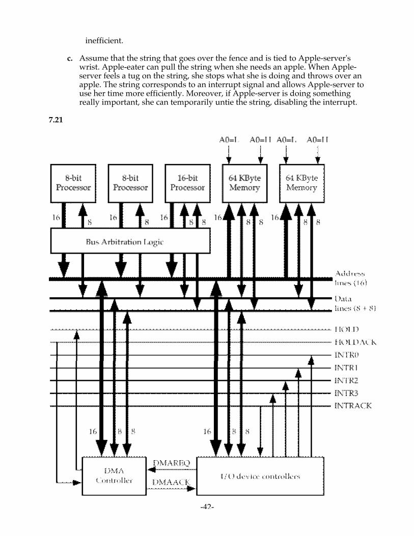
-43-
AA NSWERS TO NSWERS TO QQ U E S T I O N SU E S T I O N S
8.1 The operating system (OS) is the software that controls the execution of programson a processor and that manages the processor's resources.
8.2 Program creation: The operating system provides a variety of facilities and services,such as editors and debuggers, to assist the programmer in creating programs.Program execution: A number of tasks need to be performed to execute a program.Instructions and data must be loaded into main memory, I/O devices and filesmust be initialized, and other resources must be prepared. Access to I/O devices:Each I/O device requires its own peculiar set of instructions or control signals foroperation. Controlled access to files: In the case of files, control must include anunderstanding of not only the nature of the I/O device (disk drive, tape drive) butalso the file format on the storage medium. System access: In the case of a shared orpublic system, the operating system controls access to the system as a whole and tospecific system resources. Error detection and response: A variety of errors canoccur while a computer system is running. Accounting: A good operating systemwill collect usage statistics for various resources and monitor performanceparameters such as response time.
8.3 Long-term scheduling: The decision to add to the pool of processes to be executed.Medium-term scheduling: The decision to add to the number of processes that arepartially or fully in main memory. Short-term scheduling: The decision as to whichavailable process will be executed by the processor
8.4 A process is a program in execution, together with all the state informationrequired for execution.
8.5 The purpose of swapping is to provide for efficient use of main memory for processexecution.
8.6 Addresses must be dynamic in the sense that absolute addresses are only resolvedduring loading or execution.
8.7 No, if virtual memory is used.
8.8 No.
8.9 No.
8.10 The TLB is a cache that contains those page table entries that have been mostrecently used. Its purpose is to avoid, most of the time, having to go to disk toretrieve a page table entry.
CHAPTER 8OPERATING SYSTEM SUPPORT

-44-
AA NSWERS TO NSWERS TO PP R O B L E M SR O B L E M S
8.1 The answers are the same for (a) and (b). Assume that although processoroperations cannot overlap, I/O operations can.
1 Job: TAT = NT Processor utilization = 50%2 Jobs: TAT = NT Processor utilization = 100%4 Jobs: TAT = (2N – 1)NT Processor utilization = 100%
8.2 I/O-bound programs use relatively little processor time and are therefore favoredby the algorithm. However, if a processor-bound process is denied processor timefor a sufficiently long period of time, the same algorithm will grant the processor tothat process because it has not used the processor at all in the recent past.Therefore, a processor-bound process will not be permanently denied access.
8.3 Main memory can hold 5 pages. The size of the array is 10 pages. If the array isstored by rows, then each of the 10 pages will need to be brought into mainmemory once. If it is stored by columns, then each row is scattered across all tenpages, and each page will have to be brought in 100 times (once for each rowcalculation).
8.4 The number of partitions equals the number of bytes of main memory divided bythe number of bytes in each partition: 224/216 = 28. Eight bits are needed to identifyone of the 28 partitions.
8.5 Let s and h denote the average number of segments and holes, respectively. Theprobability that a given segment is followed by a hole in memory (and not byanother segment) is 0.5, because deletions and creations are equally probable inequilibrium. so with s segments in memory, the average number of holes must bes/2. It is intuitively reasonable that the number of holes must be less than thenumber of segments because neighboring segments can be combined into a singlehole on deletion.
8.6 a. Split binary address into virtual page number and offset; use VPN as index intopage table; extract page frame number; concatenate offset to get physicalmemory address
b. (i) 1052 = 1024 + 28 maps to VPN 1 in PFN 7, (7 × 1024+28 = 7196)(ii) 2221 = 2 × 1024 + 173 maps to VPN 2, page fault(iii) 5499 = 5 × 1024 + 379 maps to VPN 5 in PFN 0, (0 × 1024+379 = 379)
8.7 With very small page size, there are two problems: (1) Because very little data isbrought in with each page, there will need to be a lot of I/O to bring in the manysmall pages. (2) The overhead (page table size, length of field for page number) willbe disproportionately high.
If pages are very large, main memory will be wasted because the principle oflocality suggests that only a small part of the large page will be used.
8.8 9 and 10 page transfers, respectively. This is referred to as "Belady's anomaly," andwas reported in "An Anomaly in Space-Time Characteristics of Certain ProgramsRunning in a Paging Machine," by Belady et al, Communications of the ACM, June1969.

-45-
8.9 A total of fifteen pages are referenced, the hit ratios are:
N 1 2 3 4 5 6 7 8Ratio 0/15 0/15 2/15 3/15 5/15 8/15 8/15 8/15
8.10 The principal advantage is a savings in physical memory space. This occurs fortwo reasons: (1) a user page table can be paged in to memory only when it isneeded. (2) The operating system can allocate user page tables dynamically,creating one only when the process is created.
Of course, there is a disadvantage: address translation requires extra work.
8.11 The machine language version of this program, loaded in main memory starting ataddress 4000, might appear as:
4000 (R1) ← ONE Establish index register for i4001 (R1) ← n Establish n in R24002 compare R1, R2 Test i > n4003 branch greater 40094004 (R3) ← B(R1) Access B[i] using index register R14005 (R3) ← (R3) + C(R1) Add C[i] using index register R14006 A(R1) ← (R3) Store sum in A[i] using index register R14007 (R1) ← (R1) + ONE Increment i4008 branch 40026000-6999 storage for A7000-7999 storage for B8000-8999 storage for C9000 storage for ONE9001 storage for n
The reference string generated by this loop is
494944(47484649444)1000
consisting of over 11,000 references, but involving only five distinct pages.
8.12 The S/370 segments are fixed in size and not visible to the programmer. Thus,none of the benefits listed for segmentation are realized on the S/370, with theexception of protection. The P bit in each segment table entry provides protectionfor the entire segment.
8.13 On average, p/2 words are wasted on the last page. Thus the total overhead orwaste is w = p/2 + s/p. To find the minimum, set the first derivative to 0.
dwdp
=12−sp2
= 0
p = 2s
8.14 There are three cases to consider:

-46-
Location of referencedword
Probability Total time for access in ns
In cache 0.9 20Not in cache, but in mainmemory
(0.1)(0.6) = 0.06 60 + 20 = 80
Not in cache or mainmemory
(0.1)(0.4) = 0.04 12ms + 60 + 20 = 12000080
So the average access time would be:
Avg = (0.9)(20) + (0.06)(80) + (0.04)(12000080) = 480026 ns
8.15
232 memory211 page size
= 221 page frames
Segment: 0123
0
7
Page descriptortable
00021ABC
Main memory(232 bytes)
232 memory211 page size
= 221 page frames
a. 8 × 2K = 16Kb. 16K × 4 = 64Kc. 232 = 4 GBytes
8.16 •The starting physical address of a segment is always evenly divisible by 1048, i.e.,its rightmost 11 bits are always 0.
•Maximum logical address space = 29 = 512 segments (× 222 bytes/segment) = 231bytes.
•Format of logical address:
segmentnumber (9) offset (22)

-47-
•Entries in the mapping table: 29 = 512.•Number of memory management units needed = 4.•Each 9-bit segment number goes to an MMU; 7 bits are needed for the 128-entry
table, the other 2 most significant bits are decoded to select the MMU.•Each entry in the table is 22 bits.
8.17 a.page number
(5) offset (11)
b. 32 entries, each entry is 9 bits wide.c. If total number of entries stays at 32 and the page size does not change, then
each entry becomes 8 bits wide.
8.18 The system operator can review this quantity to determine the degree of "stress" onthe system. By reducing the number of active jobs allowed on the system, thisaverage can be kept high. A typical guideline is that this average should be keptabove 2 minutes. This may seem like a lot, but it isn't.

-48-
AA NSWERS TO NSWERS TO QQ U E S T I O N SU E S T I O N S
9.1 Sign–Magnitude Representation: In an N-bit word, the left-most bit is the sign (0 =positive, 1 = negative) and the remaining N – 1 bits comprise the magnitude of thenumber. Twos Complement Representation: A positive integer is represented as insign magnitude. A negative number is represented by taking the Booleancomplement of each bit of the corresponding positive number, then adding 1 to theresulting bit pattern viewed as an unsigned integer. Biased representation: A fixedvalue, called the bias, is added to the integer.
9.2 In sign-magnitude and twos complement, the left-most bit is a sign bit. In biasedrepresentation, a number is negative if the value of the representation is less thanthe bias.
9.3 Add additional bit positions to the left and fill in with the value of the original signbit.
9.4 Take the Boolean complement of each bit of the positive number, then adding 1 tothe resulting bit pattern viewed as an unsigned integer.
9.5 When the operation is performed on the n-bit integer –2n–1 (one followed by n – 1zeros).
9.6 The twos complement representation of a number is the bit pattern used torepresent an integer. The twos complement of a number is the operation thatcomputes the negation of a number in twos complement representation.
9.7 The algorithm for performing twos complement addition involves simply addingthe two numbers in the same way as for ordinary addition for unsigned numbers,with a test for overflow. For multiplication, if we treat the bit patterns as unsignednumbers, their magnitude is different from the twos complement versions and sothe magnitude of the result will be different.
9.8 Sign, significand, exponent, base.
9.9 An advantage of biased representation is that nonnegative floating-point numberscan be treated as integers for comparison purposes.
9.10 Positive overflow refers to integer representations and refers to a number that islarger than can be represented in a given number of bits. Exponent overflow refersto floating point representations and refers to a positive exponent that exceeds themaximum possible exponent value. Significand overflow occurs when theaddition of two significands of the same sign result in a carry out of the mostsignificant bit.
CHAPTER 9COMPUTER ARITHMETIC

-49-
9.11 1. Check for zeros. 2. Align the significands. 3. Add or subtract the significands.4. Normalize the result.
9.12 To avoid unnecessary loss of the least significant bit.
9.13 Round to nearest: The result is rounded to the nearest representable number.Round toward +∞: The result is rounded up toward plus infinity. Round toward–∞: The result is rounded down toward negative infinity. Round toward 0: Theresult is rounded toward zero.
AA NSWERS TO NSWERS TO PP R O B L E M SR O B L E M S
9.1 Sign Magnitude: 512 = 0000 0010 0000 0000–29 = 1000 0000 0001 1101
Two’s Complement: 512 = 0000 0010 0000 0000–29 = 1111 1111 1110 0011
9.2 1101011: Because this starts with a leftmost 1, it is a negative number. Themagnitude of the negative number is determined by flipping the bits and adding 1:
0010100 + 1 = 0010101
This is 21, so the original value was –21.
0101101
Because this starts with a leftmost 0, it is a positive number and we just computethe magnitude as an unsigned binary number, which is 45.
9.3 a. A = − 2n−1 − 1( )an−1 + 2 i ai
i=0
n−2∑
b. From –(2n–1 – 1) through (2n–1 – 1)c. (1) Add the two numbers as if they were unsigned integers. (2) If there is a carry
out of the sign position, then add that bit to the first bit position of the result andpropagate carries as necessary. This is known as the end-around carry rule. (3)An overflow occurs if two positive numbers are added and the result is negativeof if two negative numbers are added and the result is positive.
9.4 sign-magnitude ones complementRange –(2n–1 – 1) to (2 n–1 – 1) –(2n–1 – 1) to (2n–1 – 1)Number ofrepresentations of 0 2 2Negation Complement the sign bit Complement each bitExpansion of bitlength
Move the sign bit to the newleftmost bit; fill in with zeros
Fill all new bitpositions to the leftwith the sign bit
Subtract B from AComplement the sign bit of B andadd B to A using rules for additionof sign-magnitude numbers
Take the onescomplement of B andadd it to A
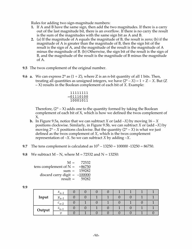
-50-
Rules for adding two sign-magnitude numbers:1. If A and B have the same sign, then add the two magnitudes. If there is a carry
out of the last magnitude bit, there is an overflow. If there is no carry the resultis the sum of the magnitudes with the same sign bit as A and B.
2. (a) If the magnitude of A equals the magnitude of B, the result is zero; (b) if themagnitude of A is greater than the magnitude of B, then the sign bit of theresult is the sign of A, and the magnitude of the result is the magnitude of Aminus the magnitude of B. (b) Otherwise, the sign bit of the result is the sign ofB, and the magnitude of the result is the magnitude of B minus the magnitudeof A.
9.5 The twos complement of the original number.
9.6 a. We can express 2n as (1 + Z), where Z is an n-bit quantity of all 1 bits. Then,treating all quantities as unsigned integers, we have (2n – X) = 1 + Z – X. But (Z– X) results in the Boolean complement of each bit of X. Example:
11111111–01110100
10001011
Therefore, (2n – X) adds one to the quantity formed by taking the Booleancomplement of each bit of X, which is how we defined the twos complement ofX.
b. In Figure 9.5a, notice that we can subtract X or (add –X) by moving 16 – Xpositions clockwise. Similarly, in Figure 9.5b, we can subtract X or (add –X) bymoving 2n – X positions clockwise. But the quantity (2n – X) is what we justdefined as the twos complement of X, which is the twos complementrepresentation of –X. So we can subtract X by adding –X.
9.7 The tens complement is calculated as 105 – 13250 = 100000 -13250 = 86750.
9.8 We subtract M – N, where M = 72532 and N = 13250:
M = 72532tens complement of N = +86750
sum = 159282discard carry digit = –100000
result = 59282
9.9xn–1 0 0 0 0 1 1 1 1yn–1 0 0 1 1 0 0 1 1Inputcn–2 0 1 0 1 0 1 0 1zn–1 0 0 1 0 1 0 1 1Output
v 0 1 0 0 0 0 1 0

-51-
9.10 +6 00000110+13 00001101+19 00010011
–6 11111010+13 00001101 +7 00000111
+6 00000110–13 11110011 –7 11111001
–6 11111010–13 11110011–19 11101101
9.11 Add the twos complement, and check for overflow. For b, we must first sign-extend the second term.
a. 111000 b. 11001100 c. 111100001111 d. 11000011 + 001101 + 00010010 + 001100001101 + 00011000 1 000101 11011110 1 001000011100 11011000
In all cases, the signs of the two numbers to be added are different, so there is nooverflow.
9.12 The overflow rule was stated as follows: If two numbers are added, and they areboth positive or both negative, then overflow occurs if and only if the result hasthe opposite sign. There are four cases:•Both numbers positive (sign bit = 0) and no carry into the leftmost bit position:
There is no carry out of the leftmost bit position, so the XOR is 0. The result has asign bit = 0, so there is no overflow.
•Both numbers positive and a carry into the leftmost bit position: There is no carryout of the leftmost position, so the XOR is 1. The result has a sign bit = 1, so thereis overflow.
•Both numbers negative and no carry into the leftmost position: There is a carryout of the leftmost position, so the XOR is 1. The result has a sign bit of 0, so thereis overflow.
•Both numbers negative and a carry into the leftmost position. There is a carry outof the leftmost position, so the XOR is 0. The result has a sign bit of 1, so there isno overflow.
Therefore, the XOR result always agrees with the presence or absence of overflow.
9.13 An overflow cannot occur because addition and subtraction alternate. As aconsequence, the two numbers that are added always have opposite signs, acondition that excludes overflow.
9.14 A Q Q–1 M0000 1010 0 0101 Initial0000 0101 0 0101 Shift 1011 0101 0 0101 A ← A – M1101 1010 1 0101 Shift0010 1010 1 0101 A ← A + M0001 0101 0 0101 Shift1100 0101 0 0101 A ← A – M1110 0010 1 0101 Shift

-52-
9.15 Using M=010111 (23) and Q = 010011 (19) we should get 437 as the result.
A Q Q–1 M000000 010111 0 010011 Initial101101 010111 0 010011 A ← A – M110110 101011 1 010011 Shift111011 010101 1 010011 Shift111101 101010 1 010011 Shift010000 101010 1 010011 A ← A + M001000 010101 0 010011 Shift110101 010101 0 010011 A ← A – M111010 101010 1 010011 Shift001101 101010 1 010011 A ← A + M000110 110101 1 010011 Shift
Answer = 0001 1011 0101 (which is 437)
9.16 An n-digit number in base B has a maximum value of Bn – 1. We need to show thatthe maximum product is less than B2n – 1.
(Bn – 1) (Bn – 1) = B2n – 2Bn + 1 ≤ B2n – 1.
The inequality is true if
–2Bn + 1 ≤ –1 or 1 ≤ Bn
This is always true for B ≥ 2 and n ≥ 1.

-53-
9.17 A Q M00000000 10010011 1011 Initial00000001 00100110 1011 Shift11110110 1011 A ← A – M00000001 00100110 1011 Restore00000010 01001100 1011 Shift11110111 1011 A ← A – M00000010 01001100 1011 Restore00000100 10011000 1011 Shift11111001 1011 A ← A – M00000100 10011000 1011 Restore00001001 00110000 1011 Shift11111100 1011 A ← A – M00001001 00110000 1011 Restore00010010 01100000 1011 Shift00000111 1011 A ← A – M00000111 01100001 1011 Q0 ← 100001110 11000010 1011 Shift00000011 1011 A ← A – M00000011 11000011 1011 Q0 ← 100000111 10000110 1011 Shift11111100 1011 A ← A – M00000111 10000110 1011 Restore00001111 00001100 1011 Shift00000100 1011 A ← A – M00000100 00001101 1011 Q0 ← 1
9.18 The nonrestoring division algorithm is based on the observation that a restorationin iteration I of the form A(I) ← A(I) + M is followed in iteration (I + 1) by thesubtraction A(I+1) ← 2A(I) – M. These two operations can be combined into asingle operation: A(I+1) ← 2A(I) + M.
9.19 False. For a negative quotient, truncation yields a larger number.

-54-
9.20 Divisor = 13 = (001101)2 is placed in M register.Dividend = –145 = (111101101111)2 is placed in A and Q registers
A Q M111101 101111 001101 Initial111011 011110 Shift001101 Add001000111011 011110 Restore110110 111100 Shift001101 Add000011110110 111100 Restore101101 111000 Shift001101 Add111010 111001 Q0 ← 1110101 110010 Shift001101 Add000110110101 110010 Restore101011 100100 Shift001101 Add111000 100101 Q0 ← 1110001 001010 Shift001101 Add111110 001011 Q0 ← 1
Remainder = (111110)2 = –2Quotient = twos complement of 001011 = (110101)2 = –11
9.21 a. Planck's constant:6.63 × 10⁻²⁷ → 0.00000000000000000000000000663
29
b. Avogadro's number:
6.02 × 10²³ → 602000000000000000000000.024

-55-
To represent the approximation of Planck's constant 29 radix-10 fractionaldigits are needed, while representing the approximation of Avogadro's numberrequires 24 integer decimal digits. To represent the approximations of bothPlanck's constant and Avogadro's number in a fixed-point number format, 29 +54 = 53 radix-10 digits are needed.
b. In the considered radix-10 base-10 biased representation for the exponent (suchthat Ebiased = E + 50), the exponent of both Planck's constant and Avogadro'snumber can be represented using 2 digits, because 27+50 = 23 and 23+50 = 73.To represent the significands, 3 radix-10 digits are needed. Therefore, torepresent the approximations of both Planck's constant and Avogadro'snumber in a floating-point radix- 10 base-10 number format, 3 + 2 = 5 decimaldigits are needed. Source: [ERCE04]
9.22 a. bX–q(1 – b–p), b–q–p
b. bX–q(1 - b–p), b–q–1
9.23 a. 1 10000001 01000000000000000000000b. 1 10000001 10000000000000000000000c. 1 01111111 10000000000000000000000d. 384 = 110000000 = 1.1 × 21000
Change binary exponent to biased exponent:127 + 8 = 135 = 10000111Format: 0 10000111 00000000000000000000000
e. 1/16 = 0.0001 = 1.0 × 2–100
127 – 4 = 123 = 01111011Format: 0 01111011 00000000000000000000000
f. –1/32 = –0.00001 = –1.0 × 2–101
127 – 5 = 122 = 01111010Format: 0 01111010 00000000000000000000000
9.24 a. –28 (don't forget the hidden bit)b. 13/16 = 0.8125c. 2

-56-
9.25 In this case, the exponent has a bias of 3. Special cases are shaded in the table. Thefirst shaded column contains the denormalized numbers. It is worthwhile to studythis table to get a feel for the distribution and spacing of numbers represented inthis format.
Exponentsign bit andsignificand
000 001 010 011 100 101 110 1110 000 0 0.25 0.5 1 2 4 8 +∞0 001 0.03125 0.28125 0.5625 1.125 2.25 4.5 9 NaN0 010 0.0625 0.3125 0.625 1.25 2.5 5 10 NaN0 011 0.09375 0.34375 0.6875 1.375 2.75 5.5 11 NaN0 100 0.125 0.375 0.75 1.5 3 6 12 NaN0 101 0.15625 0.40625 0.8125 1.625 3.25 6.5 13 NaN0 110 0.1875 0.4375 0.875 1.75 3.5 7 14 NaN0 111 0.21875 0.46875 0.9375 1.875 3.75 7.5 15 NaN1 000 –0 –0.25 –0.5 –1 –2 –4 –8 –∞1 001 –0.03125 –0.28125 –0.5625 –1.125 –2.25 –2.5 –9 NaN1 010 –0.0625 –0.3125 –0.625 –1.25 –2.5 –5 –10 NaN1 011 –0.09375 –0.34375 –0.6875 –1.375 –2.75 –5.5 –11 NaN1 100 –0.125 –0.375 –0.75 –1.5 –3 –6 –12 NaN1 101 –0.15625 –0.40625 –0.8125 –1.625 –3.25 –6.5 –13 NaN1 110 –0.1875 –0.4375 –0.875 –1.75 –3.5 –7 –14 NaN1 111 –0.21875 –0.46875 –0.9375 –1.875 –3.75 –7.5 –15 NaN
9.26 a. 1.0 = +1/16 × 161 = 0 100 0001 0001 0000 0000 0000 0000 0000b. 0.5 = +8/16 × 160 = 0 100 0000 1000 0000 0000 0000 0000 0000c. 1/64 = +4/16 × 16–1 = 0 011 1111 0100 0000 0000 0000 0000 0000d. 0.0 = +0 × 16–64 = 0 000 0000 0000 0000 0000 0000 0000 0000e. –15.0 = –15/16 × 161 = 1 100 0001 1111 0000 0000 0000 0000 0000f. 5.4 × 10–79 ≈ +1/16 × 16–64 = 0 000 0000 0000 0000 0000 0000 0000 0000g. 7.2 × 1075 ≈ 1 × 1663 = 0 111 1111 1111 1111 1111 1111 1111 1111h. 65535 = 164 –1 = 0 100 0100 1111 1111 1111 1111 0000 0000
9.27 Step 1: Sign positiveStep 2: Extract the exponent (5B)16 and subtract the bias (40)16, yielding
(1B)16 = 27Step 3: The significand (CA 0000)16 = 12/16 + 10/256 = 0.7890625.The decimal result is 0.7890625 × 1627.
9.28 The base is irrelevanta. Bias = 26–1 = 25 = 32b. Bias = 27–1 = 26 = 64

-57-
9.29
Expressible NegativeNumbers
NegativeOverflow
PositiveOverflow
NegativeUnderflow
Zero
PositiveUnderflow
Expressible PositiveNumbers
0 0.5 × 2–1022– 0.5 × 2–1022– (1 – 2–53) × 21023 (1 – 2 –53) × 21023
9.30 a. 1. Express the number in binary form: 1011010000 (normalize to 1.1bbbb)2. Normalize the number into the form 0.1bbbbbbbbbbbbb
0.1011010000 × 2k where k = 10(base10) or 1010(base2)0.1011010000 × 2(1010)
Once in normalized form every number will have a 1 after the decimalpoint. We do not need to store this number; it is implicit. Therefore in theSignificand field we will store 01101000000000000000000.
3. For the 8-bit exponent field, a bias of 128 is used. Add the bias to theexponent and store the answer: 1010 + 10000000 = 1001010
4. Sign bit = 15. Result = 1 1001010 01101000000000000000000
b. We have 0.645 = 0.101001...; therefore the significand is 01001 (the first 1 isimplicit). The sign = 0, and the exponent = 0.Result: 0 0000000 01001000000000000000000
9.31 There are 232 different bit patterns available. However, because of special cases, notall of these bit patterns represent unique numbers. In particular, an exponent of allones together with a nonzero fraction is given the value NaN, which means Not aNumber, and is used to signal various exception conditions. Because the fractionfield is 23 bits, the number of nonzero fractions is 223 – 1. The sign bit may be 0 or 1for this case, so the total number of NaN values is 224 – 2. Therefore, the number ofdifferent numbers that can be represented is 232 – 224 + 2. This number includesboth plus and minus zero and plus and minus infinity. If we exclude minus zeroand plus and minus infinity, then the total is 232 – 224 –1.
9.32 We have 0.4 × 20. Because 0.4 is less than 0.5, this is not normalized. Thus, werewrite as
0.4 = 0.8 × 2–1
Next, convert 0.8 to binary, we have repeating binary number: 0.110011001100...The closest we can get (7 bits) is 0.1100110. Converting this back to decimal, wehave
(1/2 + 1/4 + 1/32 + 1/64) × 2-1 = 0.3984375
The relative error is 0.4 - 0.39843750.4 = 0.0039
9.33 EA = A - A'A

-58-
Truncation: EA = 1.427 - 1.421.427 = 0.0049
Rounding: EA = 1.427 -1.431.427 = –0.0021
9.34 Cancellation reveals previous errors in the computation of X and Y. For example, ifε is small, we often get poor accuracy when computing f(x + ε) - f(x), because therounded calculation of f(x + ε) destroys much of the information about ε. It isdesirable to rewrite such formulas as ε × g(x,ε), where g(x,ε) = f (x +ε ) − f (x)
ε is
first computed symbolically. Thus, if f(x) = x2, then g(x,ε) = 2x + ε; if f(x) = x ,then g(x,ε) = 1
x + ε + x .
9.35 We have
EA = A - A'A = 1 – A'
A
A' = A(1 – EA)B' = B (1 – EB)A'B' = AB (1 – EA)(1 -EB) = AB [1– (EA +EB) + EAEB ]
≈ AB [1– (EA + EB)]
The product term EAEB should be negligible in comparison to the sum.ConsequentlyEAB = EA +EB.
9.36 a. EA = 0.22288 - 0.22280.2228 = 0.00036
EB = 0.22211 - 0.22210.22211 = 0.00045
b. C = A – B = 0.00077 C'= A' – B' = 0.0007 EC = 0.00077 - 0.0007
0.00077 = 0.09
9.37 a. (2.50000 × 10–60) × (3.50000 × 10–43) = 8.75000 × 10–103 → 0.00088 × 10–99
The otherwise exact product underflows and must be denormalized byfour digits. The number then requires rounding.
b. (2.50000 × 10–60) × (3.50000 × 10–60) = 8.75000 × 10–120 → 0.0The intermediate result falls below the underflow threshold and must be
set to zero.c. (5.67834 × 10–97) – (5.67812 × 10–97) = 2.20000 × 10–101 → 0.02200 × 10–99
This example illustrates how underflowed sums and differences ofnumbers in the same format are always free from rounding errors.
-59-
9.38 a. The exponents are equal. Therefore the mantissas are added, keeping thecommon exponent, and the sum is renormalized if necessary.
5.566 × 10³ + 7.777 × 103 = 1.3343 × 10³ ≈ 1.334 × 10³
b. The exponents must be equalized first.3.344 × 101 + 8.877 × 10–2 = 3.344 × 101 + 0.008877 × 101 =
3.352877 × 101 ≈ 3.352 × 101
9.39 a. 7.744 × 10⁻³ – 6.666 × 10–3 = 1.078 × 10⁻³
b. 8.844 × 10⁻³ – 2.233 × 10–1 = 0.08844 × 10⁻¹ – 2.233 × 10–1 =–2.14456 × 10⁻¹ ≈ –2.144 × 10⁻¹
9.40 a. 2.255 × 101 × 1.234 × 100 = 2.58267 × 101 ≈ 2.582 × 101
b. 8.833 × 10² ÷ 5.555 × 104 = 1.590 × 10⁻²