some prospective applications of silicon electrodeposition from molten fluorides to solar cell...
TRANSCRIPT

Journal o f Electronic Materials, Vol. 6 , N o . 6 , 1977
SOME PROSPECTIVE APPLICATIONS OF SILICON ELECTRODEPOSITIONFROM M O L T E N FLUORIDES TO S O L A R CELL FABRICATION*
Uri Cohen
Center for Materials ResearchStanford University
Stanford, California 94305
(Received April 7, 1977)
Electrodeposition of both epitaxial and polycrystallinecontinuous films of dense, coherent, and well-adherent sili-con coatings was achieved from m o l t e n fluorides. A dis-solving Si anode and an operating temperature of about 750°Cwere utilized. Silicon electrocrystallization epitaxy (ECE)produced films with the (iii) orientation on Si substratesof the same orientation. The unintentionally d o p e d filmswere of p-type character with a resistivity in the range0.05 - 0.i0 ~-cm. Polycrystalline Si films were similarlyelectroplated onto various polycrystalline m e t a l substrates.Uniform coherent, and well-adherent coatings with g r a i n di-ameters as large as 40 - 50 ~m were obtained. The usefulrate of electrodeposition of Si could be significantly in-creased by the application of an alternating square wavep u l s e (ASWP)2technique. Cathodic current pulses as highas 300 m A / c m (growth rate of a b o u t 5 ~m/min) were demon-strated. The cathodic current efficiencies, for all m o d e sof growth, were a b o u t 70 - 100%. The effects of the variousoperating parameters, and some prospective applications tothe fabrication of solar cells, are discussed.
Key Words: Si-electrodepositlon, solar cells, Si-epltaxlalfilms, Si-polycrystalllne films, M o l t e nfluorides.
6 0 7
© 1977 by the American Institute of Mining, Metallurgical, and Petroleum Engineers, Inc. No partof this publication may be reproduced, storexiin a retrieval system, or transmitted, in any form orby any means, electronic, mechanical, photocopying, microfilming, recording, or otherwise, with-out written permission of the publisher.

608 Cohen
Introduction
The present cost of silicon solar cell fabricationis prohibitively high for commercial large-scale terres-trial applications. A drastic cost reduction by means ofnew inexpensive processing methods is, therefore, highlydesirable.
Electrodeposition of Si may offer some unique advan-tages over more conventional processes. It is a relativelylow temperature process (e.g., 750°C), and is quite tole-rant to large temperature fluctuations. L a r g e areas arerelatively easy to plate, and the substrate shape may beq u i t e complex. Coating uniformity depends only on the cur-rent density distribution, and the coating thickness iseasily controlled by simple parameters such as current (orpotential) magnitude, and the plating time duration. Eco-nomic factors seem to favor the electrodeposition processand the technique is both safe and familiar to the indus-try.
Silicon powders, along with potassium, were firstelectrodeposited from a molten fluoride mixture (KF-K2SiF6)in 1865, by U l l i k (i). Electrowinning of silicon from otherbaths, m o s t l y oxide-containing, and in particular Si02, hassince been reported by many o t h e r investigators (2)-(12).The electroplating of coherent, crystalline elemental sili-con, however, has not been reported to date. Usually,powdery, dendritic, or other particulate Si deposits havebeen obtained. Such products require separation from theelectrolyte by crushing, leaching, and washing. Further,an additional melting step is also required. The product soobtained, may include a high level of impurities due to bathinclusions and adsorption. To avoid these problems, w h i c hare related to the electrocrystallization of Si, liquidalloys of A I - S i and Cu-Si have been suggested (3)-(6) foruse as cathodes. The use of such liquid alloys is thussimilar to the electrowinning processes of AI or Mg, w h i c hare collected as liquid m e t a l cathodes, and are readilyseparated from the electrolyte by density difference. Theutilization of m o l t e n silicon-alloys, however, requires afurther separation step of Si from the alloying metal(e.g., AI or Cu). These processes were recently evaluatedby Hunt, Crossman, and Wolf (13) for the production of"solar-cell grade" silicon. They evaluated these processes

Some Prospective Applications of Silicon 609
to be non-advantageous due to a higher production costthan the conventional process of producing the "metallur-gical-grade" silicon, with similar p u r i t y level.
Some time ago, a general m e t h o d for electroplatingcoherent and d e n s e refractory m e t a l coatings from all-fluoride baths was developed by Senderoff and Mellors (14),(15),(16). They succeeded in obtaining coherent coatingsof eight of the nine refractory metals of Groups IVB, VB,and VIB. The m e l t s contained a eutectic solvent of alkali-fluorides, and an appropriate fluoride salt of the refrac-tory metal. Similarly, Cook et al. (17) developed a m e t a l -liding process from all-fluoride baths, in w h i c h the m e t a l -liding element was simultaneously electrodeposited and dif-fused into another base m e t a l substrate to form a smoothand dense a l l o y coating. Excellent silicide coatings (18),as well as many other diffused a l l o y coatings (19), werereported by Cook. Several attractive features of thesealkali-fluoride solvents have been described elsewhere (17),(20),(21). The most important features are (i) the abilityto flux the surface oxides thereby exposing a c l e a n metallicsurface to the solution, (2) high stability of the fluorideion complexes, (3) high ionic conductivity, (4) low m e l t -ing point eutectics, (5) low v a p o r pressure, (6) low vis-cosity, and (7) a large decomposition potential range( > 3 V ) . T h e s e features combine to make the alkali-fluoridem e l t s ideal electrolytes for the electroplating of manym e t a l s and alloys.
The ultimate absence of bath impurities, and in par-ticular oxides, seems to the author to be crucial for suc-cessful electroplating of coherent and high quality siliconcoatings. This subject is further discussed in this paper.Utilizing extensive purification techniques of the fluoridemelts, the successful electroplating of coherent elementalsilicon in both epitaxial films (20),(21),(22) and poly-crystalline films (20),(23),(24) has been achieved for thefirst time.
Experimental Procedures
A schematic drawing of the experimental set-up iss h o w n in Fig. i. It has been described in detail in pre-v i o u s publications (20),(21). An inert atmosphere of

610 Cohen
STAINLESS S'i"GROUND JOINT
~ Ni RODTEFLON GROUND JOINT
He AND VACUUM OUT
He IN
RESCUE CHAMBER--,--,.~
CIRCLE SEAL VALVE =
VACUUM"-,,.~
COOLINGW A T E R ~
LIGHT BULB" !-'----~1A N O D E ~°
TH ERMOCOUPLE--------9
0REFERENCE oELECTRODE- oO
OOOOOOO
lr
OUT
-He IN(BUBBLER)~ V I E W I N G PORT
I
(REMOVABLE THROUGHCIRCLE SEAL VALVE)
LINER
lACE
L ~ " ~ ' ~ INCONEL CANCRUCIBLEOF SALTS
F i g u r e I . Schematic d r a w i n g of t h e experimental a p p a r a t u s , (Courtesy of t h eElectrochemical Society, Re£erence2 I.)

Some Prospective Applications of Silicon 611
purified helium was maintained in the chamber (with a slowflow rate). The electrodes were insulated from each otherand from the chamber, and could be easily replaced throughspecial "rescue chambers" (shown in Fig. i, and furtherdescribed in Reference 20).
A salt mixture of 5 m o l . % K2SiF6, i0 m o l . % KHF2,balance L i F - K F (47.5 - 37.5 mol.%) was first m e l t e d in them a n n e r described elsewhere (20),(22). KHF2 slowly decom-posed into KF and HF, the latter reacting with residualoxides according to the equation
-22HF(sol ,n) + O ( s o l , n ) = 2 F ( s o l , n ) + H20(vapor )
The equilibrium was shifted to the right under vacuum,removing the water v a p o r into a liquid nitrogen trap. Thisstep was followed by purging the melt with purified h e l i u mto expel any dissolved HF. A silicon anode piece was thenimmersed in the melt in order to equilibrate the siliconvalences:
Si + Si(IV) = 2Si(II) (1)
The purification procedure was completed by a pre-electrolysis step, during w h i c h metallic ions more n o b l ethan silicon, as well as some silicon, were plated onto asacrificial molybdenum strip cathode.
A practical reference electrode was established bythe simple immersion of a tungsten or silver wire, to formthe r e d o x electrode M/Si(IV),Si(II); (M = W or Ag). Thea n o d e was always a dissolving silicon p i e c e of high purity.The cathodes were silicon wafers of (iii) orientation forepitaxial growth, and W, Ag, Mo, Nb, and A g / N i for p o l y -crystalline growth.
The electrical signals were produced by the combina-tion of PARI73-PARI75. Cyclic voltammetry, steady current,and current-ASWP techniques were utilized.
The samples were analyzed by the Laue x - r a y backreflection technique for single crystallinity, by powderx - r a y patterns for the presence of other phases, and byelectron microprobe and A u g e r spectroscopy for chemicalimpurities. Scanning electron microscopy (SEM), and

612 Cohen
sample cleaving and sectioning metallography were used tos t u d y the morphology. Epitaxial films were also tested bythe hot probe technique for their conductivity type, andby the four-probe measurement technique for their resis-tivity.
Results
Si Electrode Polarization
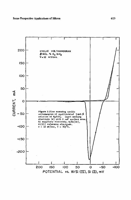
A typical I-V c u r v e obtained by slow scanning cyclicvoltammetry of the equilibrated 5 m o l . % solution of K 2 S i F6is s h o w n in Fig. 2. A tungsten strip was used here as theworking electrode. The cathodic wave, w h i c h initiates atabout -66 mV, is correlated with the deposition of Si m e t a lonto the working electrode. On the reversal of the current(at -52 mV), the anodic part is seen to be slightly shiftedto the left of the cathodic part. This indicates that thedeposition process is not completely reversible. The posi-tion of the anodic peak, w h i c h corresponds to the Si-stripping process, depends on the rate of scanning, and thepotential at w h i c h the scanning direction is switched.F i g u r e 3 shows a cyclic voltammogram w h e r e the polarizedelectrode was a silicon piece. The electrodissolution ofSi was found to be similar to that of Nb (20), with a linearcurrent dependence on the anodic potential, at least up to+450 mV. One ampere, w h i c h is the delivery limit of theinstrument, limited the measurement to this potential range.The Si a n o d e surface area in the melt was about i cm2, and^this potential yielded a current density of roughly i A/cmz.Similar to Nb (20), the anodic dissolution curve does notreveal the characteristic electropolishing active-passivetransition and current plateau.
Si Electrocrystallization Epitaxy (ECE)
Some initial results of Si ECE have been describedelsewhere (21),(22). Single-crystalline Si wafers of the(iii) orientation were used as substrates and a high puritySi piece served as the dissolving anode. The bath tem-perature was about 750°C. An anodic current pulse of50 m A / c m2 was applied to the substrate for i sec prior tothe deposition. This served to achieve an in-situ etchingof the w a f e r (approximately 150 ~). The polarity was then
Some Prospective Applications of Silicon 613
200
150
I00
5O
E
F : 0zhi
132- 5 0( j
- I 0 0
-I 5 0
- 2 0 0
I I I I
CYCLIC VOLTAMMOGRAMS M O L . % K2 SiF6V=IO m V/see.
Figure 2 .S low scanning c y c l i cvolta.~aogram of equil ibrated 5 m o l . ~so lu t ion of K2SiF6 . I n e r t workingelectrode (W) with 2 cm2 s u r f a c e area
S i auxil~ary electrode; W/SI(IV)~S ! ( I I ) r e f e r e n c e e l e c t r o d e .v = i0 mV/sec, T = 765°C.
I I ,,I I I2 0 0 150 I 0 0 5 0 0 - 5 0
P O T E N T I A L vs. W/Si OV), Si (TI'), mV- I 0 0

6 1 4 C o h e n
o '~o o . , ~I 1 I I I I I I " T '~
_ \ _ o
, 0 ~L~,
_ o ~U
g~~ 0 Q.)
_ o e g~-
0 ._I ®~- o '~ - ~ o~
o ~
- o o ~
_ ~ , ~ > _ ~ LcJ 0,-40
oo0 " H
_ ~,-~L~
_ _ ~
¢J U
if)
0I I I .I I I I I
0 0 0 0 0 0 0 0 00 0 0 0 0 0 0 0 0
I I I I I I I I I
Vw ~ N 3 ~ N D
Some Prospective Applications of Silicon 615
reversed, the Si w a f e r becoming the cathode, and constantcurrent electrodeposition established for a predeterminedperiod of time.
The current density was found to have an importantinfluence upon the morphology of the deposit. Figure 4shows SEM photographs of films w h i c h were g r o w n at i, 2,4, and 6 m A / c m2. Notice the substantial morphology improve-ment with the current increase. The poor coverage of thesu~strate surface, combined with the hillock and layerstructure of Fig. 4(a), gradually become more uniform andsmooth through Fig. 4(d). This effect, w h i c h is attributedto the favoring of normal growth over the competing processof impurity adsorption, is further discussed below.
The operatin~ current density was found to be limitedto about i0 m A / c mz. This limit was imposed by the forma-tion of polycrystalline growth on top of an initial epi- ?taxial layer. A cleaved sample w h i c h was g r o w n at i0 m A / c m~is shown in Fig. 5. An initial epitaxial film of abouti0 ~m, preceded the growth of polycrystalline Si. On theback side of the wafer, the initial epitaxial growth waseven thinner.
One of the problems encountered in the ECE of Si wasetch pitting of the Si samples in the m o l t e n bath. It wasfound that the mere immersion of a silicon w a f e r in themelt, without the application of an external current, re-sulted in severe pitting. A sample w h i c h was immersed inthe melt for one hour, is shown in Fig. 6. An interestingobservation was that the growth process could correct forthe substrate pitting; see Fig. 7. The substrate was firstimmersed in the melt for 15 minutes, then a current of2 m A / c m2 was applied. The sample was then removed from themelt as soon as the growth was completed. Etch pits exist-ing in the substrate were virtually e l i m i n a t e d i n the epi-taxial film. In addition, the pitting problem could becompletely avoided by starting the growth immediately fol-lowing the substrate immersion in the melt (and an anodiccleaning pulse), and by its removal from the melt as soonas the growth was terminated.
A similar problem was the staining or clouding of thesample surface. Figure 8(a) shows a sample with circularshiny spots. T h e s e spots were covered with frozen salt

616 Cohen
o o
v
,-4
al u r./'J
a~

S o m e Prospective Applicat ions of Si l icon 617
(a)
(b)
F i g u r e 5 M i c r o g r a p h o f a c l e a v e d s a m p l e , i C = lO mA/cm2 ( a v e r a g e ) .(a / S u b s t r a t e i n the c e n t e r3 d e p o s i t on both s i d e s .(b) A t r a n s i t i o n e p i t a x i a l l a y e r ( c e n t e r ) and a p o l y -
c r y s t a l l i n e l a y e r ( r i g h t ) .

618 Cohen
a
(b
Figure SEM photographs of an etch-pitted substrate~ after beingimmersed for one hour in the molten bath, with no appliedcurrent.

Some Prospective Applicationsof Silicon 619
(a)
(b)
Figure ? SEM photographs of a pitted substrate and an unpittedepitaxial growth, (a) Center of sample. (b) Loweredge of sample. Clinging bath salt is seen as whiteparticles.

620 Cohen
drops when the sample was removed from the melt. When thesample was held in the close vicinity of the bath allowingit to cool slowly, the vapors above the melt had a chanceto attack the exposed area. Only the spots covered by thesalt d r o p s were protected from this attack. The stainingof the surface area was undetectable by SEM analysis; seeFigs. 8(b) and (c). It was only observed by optical meansand is believed to consist of a very thin film. Since itcould not be removed by etching in HF solution, it is un-likely to be an oxide. Notice the lack of pitting on thissample. This sample was not allowed to stay unduly long inthe melt with no applied current. The r e a s o n for the largepyramids and the intermediate layered structure is presentlyunknown. The low density of the pyramids suggests that dis-locations in the substrate may be responsible. The cloudingproblem could be virtually eliminated by rapid removal ofthe sample from the hot zone a b o v e the melt following termi-nation of growth. The rapid cooling, however, may introduceappreciable stresses and dislocations in the sample.
On one occasion, the molybdenum crucible containing themolten salts developed a c r a c k in its welded seam. The saltsw h i c h leaked out, leached chromium from the Inconel chamber,and eventually contaminated the bath with chromium ions.Samples w h i c h were grown from this bath were found to con-tain Cr detectable by microprobe analysis, and revealed anunusual morphology. Figure 9 shows SEM photographs of sucha sample. Straight slits crossing the triangular flat pyra-mids were only observed in samples grown from this bath.The Cr atoms are believed to preferentially b l o c k the propa-gation of layers so that internally bounded twin lamellaeand other stacking faults form.
The g r o w n epitaxial films were characterized by Lauex - r a y back-reflection for single-crystallinity. Diffrac-tion patterns of an uncoated (iii) substrate, and (iii)substrates with g r o w n films (about i0 ~m thick) were vir-tually identical, with no extra spots arising due to theg r o w n films. In all cases, the films were found to bep-type. The w a f e r substrates, w h i c h were donated by Semi-metals, Inc., were of n-type conductivity (phosphorus doped),with a resistivity of 9 - 15 ~-cm, and were of (iii) orien-tation. The resistivity was measured by the "four-pointprobe" technique w h i c h is applicable to epitaxial films ofa different conductivity type than the substrate (25).
Some Prospective Applications of Silicon 621
o
u 0~ 0
v

62~ Cohen
Cb~
Figure 9 SEM photographs of (IIi) Si epitaxialfilm contaminated with Cr.

Some Prospective Applications of Silicon 623
Typical resistivities of 0.05 - 0.i0 ~-cm were found. Thisrange roughly corresponds (25) to 1018 carriers/cm 3. It isequivalent to a b o u t 20 ppm in silicon, or 0.002 at.% ofelectrically active impurities. Hall mobility measurementswould have been more reliable for the determination of theimpurity content. Electron microprobe analysis, using dis-persive x - r a y energy, failed to detect any impurities inthe epitaxial films. The detection limit of this techniqueis estimated at about i00 ppm.
Polycrystalline Si Growth
Electrodeposition of polycrystalline Si was carried outfrom the same solution used for ECE (5 m o l . % K 2 S i F6 in theKF-LiF eutectic). The a n o d e was the same Si piece, and thesame W/Si(IV),Si(II) electrode was used as a reference.Non-alloying metal substrates were used for cathodes. T h e s eincluded Ag, W, and Nb. The latter two m e t a l s actuallyformed thin diffused WSi2 and NbSi 2 alloy coatings, but therate of deposition far exceeded that of diffusion at theoperating temperature (750°C).
Similar to ECE, the current density was found to havea pronounced effect on the morphology. In addition, dif-ferent substrate metals have appreciably different effectson the deposit morphology. Sluggish nucleation of the Sip h a s e on the tungsten strips was found. Figure i0 shows asample w h i c h was g r o w n at a constant cathodic current,iC = 2 m A / c m2 Difficult nucleation resulted in isolatedcrystallite growth, with occasional needle bunches, ema-nating like cactus bushes. Needles as long as 1 cm wereobtained. The substrate surface w h i c h was not covered bySi was found to be the p h a s e WSi2. Further improvement ofthe deposit uniformity was achieved by first electroplatingat iC = 4 m A / c m2 (for 3 min), and then at iC = 2 m A / c m2(for 14 hours). The initial period of the higher currentdensity served to enhance nucleation, thereby improving theuniformity, and the lower current period was intended toensure a higher quality growth. F i g u r e ii shows such asample. The entire substrate surface was covered with aSi deposit of large g r a i n diameter with good uniformity andadherence. Very few "needle bushes" were found.
In contrast to tungsten, silver substrates were foundto offer easier nucleation for the Si deposit. Figure 12

624 Cohen
,,Q I ,4 o o l I
oc~

Some ProspectiveApplications of Silicon 625
4d
U U
. ~ . y o~
v
gv~
v

626 Cohen
shows a silicon deposit w h i c h was grown on an Ag coating,on the back side of a Si wafer, at iC = 6 m A / c m2 . TheSi coating was uniform, coherent, and well adherent to thesubstrate. No needle bunches were observed. The etch pitsw h i c h are seen in Fig. 12(b) were caused by leaving thesample in the melt for 15 minutes after growth was termi-nated. Very l a r g e crystallites of Si, up to 500 ~m, wereelectrodeposited onto Nb substrates. F i g u r e 13 shows sucha deposit. It was made of individual crystallites, looselyattached to the substrate. Most of them fell off when thesample was cleaned in an ultrasonic cleaner. No needleswere observed, and the crystallite size was dependent onthe cathodic current density. The substrate surface w h i c hwas not covered by Si crystallites was found to be NbSi2.Other substrates w h i c h were tested were strips of nickelcoated with a protective Ag coating. Since Ag does notalloy with either Ni or Si, it should be effective for pre-venting the diffusion and alloying of the substrates. Pre-liminary results show that the silver coating, w h i c h wasobtained by high rate sputtering, was porous and ineffec-tive for preventing the undesired diffusion. Figure 14shows an unusual growth morphology of the compound NiRSi 9,w h i c h was obtained on a Ni strip coated with a "proteCtiVe"Ag layer 2 ~m thick. The Ag layer was apparently porous,giving rise to confined Ni diffusion through the pores inthe Ag layer, and diffusion alloying with the depositingsilicon. One may call such a process a "channel growth".
Si Eleqtrodeposition with ASWP Application
The Alternating Square Wave P u l s e (ASWP) technique,w h i c h was previously described for Nb deposition (20),(26),was also utilized for Si electrodeposition. Very littlework was done to study the effects of the technique onincreasing the rate of Si epitaxial growth and the resultsare inconclusive and require further study. However, pre-liminary efforts to apply this technique to improve theuniformity and growth rate of polycrystalline Si were quitesuccessful. Figure 15 shows a coating of Si w h i c h was de-posited onto a W substrate at iC = 4 m A / c m2, i A = 20 m A / c m2,and Q = 2.0 , w h e r e i_ and iA are the cathodic andanodic pulse current densities, respectively, and Q isdefined as Q E li~t^/iAt.l ; here t and t are the
. . ~ I ~ A . . C Acathodic and anoalc pulse perloas, respectively. A uni-form surface, with no needle bushes, was obtained. The

Some Prospective Applications of Silicon 627

628 Cohen
~ D
<a)
(b)
Figure 13 Polycrystalline Si in individual crystallites ,.electrodeposited onto Nb substrate at 0.5 mA/cm=.
(a) General view;
(b) SEM photograph of a typical crystallite.

Some Prospective Applications of Silicon 629
(a)
(b)
Fig. lh SEM of Ni3Si2 deposit on Ag(2~n)/Ni substrate.The elongated crystallites are oriented alongthe [i00] direction (orthorhombic latticestructure), i = I0 mA/cm2, T = 760°C.

630 Cohen
Cb)
F i g u r e 15 S ~ o£ Si deposit on W substrate by A~N'P.
~c ~ ~ ~ / ~ , IA ~ 2o ~ / ~ , tc = ~ ,e~,tA -- 0.5 sec; q = 2.0, 760°C, 15 hrs.

Some Prospective Applications of Silicon 631
crystallites, however, seem to be more faceted than thoseof Fig. 9, w h i c h were obtained under the same cathodiccurrent density. T h e s e Si deposits rapidly lost coherencywith increase of growth rate. F i g u r e 16 shows a samplew h i c h was g r o w n with cathodic current pulses of 40 m A / c m2.The initial globule growth eventually was replaced by anelongated, worm-like type of growth. A fascinating mor-phology was observed on the sample edges; see Fig. 16(c).At even higher rates of growth, the entire deposit becamedome-like, with the domes b e i n g composed of a very loose,hair-like, or fibrous b r o w n deposit. Figure 17 shows asample w h i c h was g r o w n with cathodic current pulses of300 m A / c m2 (growth rate of about 5 ~m/min). The current-ASW-P trace, as well as the cell voltage, V , and cathodicpotential, ~ , traces for this sample are shown in Fig. 18.Notice the transition on the voltage trace, (V-t), corre-sponding to the anodic dissolution of Si deposited on theanode during the preceding anodic p u l s e to the substrate.
Discussion and Conclusions
Impurity Adsorption and Current Density Effects
The role of impurities present in the m o l t e n bath, andspecifically the oxides and oxygen, in affecting the siliconelectrodeposit morphology has not been fully appreciated.Cook, in his siliciding process (18), attributed the de-terioration of the silicide coatings to the presence ofoxides and o x y g e n impurities. He suggested that siliconmonoxide separates out and interferes with the silicidingreaction. Most other workers, however, were less concernedwith this problem. Thus, Monnier et al. (6),(7), c l a i m e dto obtain high purity silicon deposits from m o l t e n electro-lytes based on cryolite and silica. Yet, the extensiveleaching procedures w h i c h they described for the separationof the entrapped electrolyte from the silicon product, i n d i -cate that the deposit was probably spongy and incoherent.Furthermore, the leaching and analysis procedures cast somed o u b t on the claimed purity and, in particular, the oxygencontent of the silicon deposits.
Aluminum electrolytic extraction from m o l t e n e l e c -trolytes is a commercially successful process. The elec-trolytes contain cryolite and alumina, and the oxides do

6 3 2 C o h e n
vi 5o~ul
u Z ~ 1:v
o
(5
~ u
. ~ o
s ~
~ .
~og •
•, -I w W
~ c4~

Some Prospective Applications of Silicon 633
.~ 1 5 ° l ~ I
o~ ~
' ~ . . . ~ . )
r.~

634 Cohen
~w '.LN3~1811:)0 00 0 0 0o o o o
Lo 0 tO
. . . . I I I_ • . . . . | . . . . . . . . . ] _ ~
• #
I 'I f , , , ~
- ' . . . . ~ . . . . . . . . . 7 - -m• !
I '; 0, /
- r - - - ~ .. . . . .~ - - - - ®
k _ . l , , .
- F - - - 7. . . . . - l - - i I ~- ! / -to
> " I
, 0 40 0 0 0 0 0
~ ' 0 0 0 0 0 0
AUJ '3OONV IS "SA 7 V l I N 3 1 0 c l 3C]OHlV:)
i I { { (, i i I I I0 0 0 0 0 0 0 0
~" to 0 ~ to 0 ~ 0
AW '(TT) !S'(7~[)!S/M "SA 7 ~ l l N 3 1 0 d 30OH.LV3
u l
I--
"0aJ 0
i-~ qJ0 . . ~
,-4 0
• w• , ~ 0 °
~ u ~ . 4 N
a l
0 ~
m
14

Some Prospective Applications of Silicon 635
not seem to interfere with the process. A basic dif-ference, however, exists between the electrolyticallyextracted Si and AI. Whereas AI is deposited as a liquidmetal, Si is deposited as a solid. Thus, oxides do notinterfere in the formation of a coherent liquid AI de-posit, but may interfere with the n o r m a l electrocrystal-lization of s o l i d Si. The oxygen ions can be chemicallyadsorbed onto the growing Si crystalline surfaces to formthe thermodynamically stable SiO compound (i < x < 2).Even a monoatomic layer, or justXa fraction thereof, isenough to b l o c k and hinder normal crystallization.
In the ECE process, the mere adsorption at preferredsites such as layer steps and kinks, can hinder the normallayer propagation, eventually giving rise to the formationof hillocks and macrosteps. Reducing the bath impuritycontent, or increasing the growth rate (current density)will favor the depositing ions in their competition withthe adsorbing impurities for the growth sites. The lattereffect was shown in Fig. 4.
In polycrystalline Si growth from oxide-containingelectrolytes, the adsorbed oxides eventually cover theentire crystallite, forcing new n u c l e i to form. The resultis a loose powdery deposit, with the small crystallitesbeing virtually separated from each other, and enclosed bythin oxide shells. This phenomenon is q u i t e similar to theeffect of concentration polarization (27) and has deceivedseveral workers who have attempted to improve the depositmorphology by increasing the solute concentration. It maybe noted that, whereas the effect of concentration polari-zation becomes more pronounced at high current densities,the effect of impurity adsorption is diminished with thecurrent increase. Oxide-containing electrolytes yield poormorphologies due to surface oxides at low current densities,and due to concentration polarization effects at higher cur-rent densities. A conclusion w h i c h may be d r a w n from thisdiscussion is that, in order to achieve coherent Si coatings,an ultimate bath purification step is necessary. In par-ticular, the oxygen and oxide contaminations must be totallyremoved from the m o l t e n bath.
Si ECE Problems
Several problems have been encountered in the Si ECEprocess. Current distribution across the substrate affects

636 Cohen
the film uniformity. To produce a more uniform currentdistribution, a metallic layer with greater conductivitymay be attached to the back side of the wafer, either by amechanical attachment, or as a coating or film. The metalin contact with the back side of the w a f e r should be com-patible with silicon. It must not have a low melting pointa l l o y or eutectic with silicon, and its solid solubilityin Si at the operating temperature must be as small as pos-sible. It was found that a layer of Ag m e t a l 0.5 ~ thick,obtained by sputtering, resulted in a substantial improve-ment in the uniformity of the epitaxial layer. Thickercoatings should produce even more uniform layers. Thesilver layer may be readily removed by dipping in diluteNH4OH/H202 solution, w h i c h will not attack silicon. Itssolid solubility in silicon at 750°C is extremely low, andthe Si-Ag system has only one eutectic at 840°C.
Etch pitting of Si substrates and epitaxial films isattributed to melt attack. The problem could be completelyavoided when the Si w a f e r was not allowed to unduly dip inthe melt with zero applied current. The pitting is believedto be due to Eq. (i). The pits are oriented in the [iii]direction, and are self terminating. Their density (seeFig. 6) was too high to be correlated with substrate dis-locations. L o c a l effects, however, are seen in Fig. 6.
Staining or clouding caused by the vapors above themelt, although a less severe problem, are not yet under-stood. A careful chemical analysis of the stained surfacecombined with a structural study, may provide some insightinto this problem. The author believes that the source ofthis staining is not different than that of the etch pit-ting. In fact, very shallow pitting can always be seen onthe substrate surface, a b o v e the melt contact line. Ofcourse, vapors of SiF4 a b o v e the melt may condense on thissurface and form etch-pits in a similar way to the m e l t -formed pits.
The current density range for ECE growth was quitelimited. The lower l i m i t of about i m A / c m2 was imposedby the impurity adsorption effect, and may be loweredwith smaller bath impurity content. The upper limit ofabout i0 m A / c m2 is imposed by the crystallization process.More defects are incorporated as the rate of deposition isincreased, eventually leading to the loss of crystal

Some Prospective Applications of Silicon 637
coherency and the onset of polycrystalline growth. Thisu p p e r limit is expected to be dependent on the substratetemperature. Higher temperature should enhance the mobil-ity of the n e w l y deposited atoms (adatoms) on the surface,and therefore their chance to incorporate into the correctlattice sites. Higher temperature, therefore, should raisethe upper limit of the useful current density for ECE.
Polycrystalline Si Growth
The sluggish nucleation of Si on W substrates imposessome problems in obtaining uniform coatings. A large g r a i nstructure, however, is easy to obtain and the problem isessentially confined to one of good nucleation control.Silicon coatings were more uniform and adherent on Ag sub-strates than on W or Nb substrates. The reason for thebetter uniformity is probably due to the easier nucleationon Ag. The better adherency to the Ag substrate is probab-ly due to the lack of an underlying diffused silicide alloywith Ag (W and Nb form WSi 2 and NbSi2, respectively). Also,Ag is more ductile and may easily accommodate the stressescreated by non-matching thermal expansion coefficients.For applications w h i c h require uniform and coherent Sicoatings of l a r g e g r a i n diameter, such as solar cells, aninitial nucleation step of the appropriate nuclei densityand uniformity is crucial. For W or W-coated substrates,this may mean an initial period of relatively higher cur-rent density followed by growth at a more moderate rate toensure high quality crystallization. For Ag, or Ag-coatedsubstrates, an initial nucleation period of relatively lowcurrent density may be required, followed by growth atmoderate rates. In either case, secondary nucleation ish i g h l y undesirable (for solar cells).
The application of the alternating square wave p u l s e(ASWP) technique to Si growth improved the coating uni-formity at low and moderate current pulses, but producedporous and fibrous deposits at the high cathodic currentpulses. Unfortunately, the deposits did not show theformation of large g r a i n growth at the very high rates,such as was observed in the niobium electrodeposi-tion (20),(26). Coherent Si deposits were obtained withcathodic current pulses of up to about 40 m A / c m2. Adherentdeposits, with the general appearance of domes and composedof fibrous material, were obtained at cathodic current

638 Cohen
pulses of up to 300 m A / c m2 - . These deposits may require aremelting step for any practical use. The current effi-ciency with the application of the ASWP technique wasusually better than 90%.
Film Impurities and Doping
Although intentional doping of the Si deposits wasnot attempted in this work, in principle this should beeasily accomplished. Impurities are incorporated intothe deposit either by co-deposition, or by adsorption.Most metallic impurities, w h i c h govern the electricalproperties of silicon, are incorporated by co-deposition.Adsorption effects, w h i c h were discussed above, are con-sidered to be deleterious, and are not discussed here.
The principles of co-depositlon have been discussedelsewhere (20),(28). For equilibrium co-deposition oftwo metals M and N, the alloy composition is g i v e n from
(aM) i/m (aM+m) i/m
= i/n " exp ~ (E M - E N) (2)(aN)i/n (aN+n)
W h e r e a M and aN are the alloy activities of the com-ponents M and N , respectively, in the deposited solid,
and a +n are the activities of the respective ions~'nMq~the solution, F is Faraday's constant, and m and nare the number of electrons transferred to deposit M orN atoms, respectively. E$ and E~ are the standard elec-trode potentials defined ~or the s~andard states (pure sub-stances), for w h i c h aM= aM+m = i , and aN=aN+n = i ,respectively.
If, for example, Si is introduced in Eq. (2) insteadof m e t a l N , and the impurity instead of m e t a l M , thenEq. (2) can be used to predict the impurity content in Sias a function of the bath composition. Of course, forsuch predictions, previous knowledge of the standard elec-trode potentials (or their difference), and that the depo-sition process is u n d e r conditions close to equilibrium isrequired.
A numerical example may illustrate this point. Sup-pose a doping level of i ppm AI is required to produce a

Some Prospective Applications of Silicon 639
silicon deposit of p-type conductivity (resistivity ofabout 0.7 ohm-cm). For Si n = 4 , and for AI, m = 3.The standard electrode potentials* are t a k e n from W i c k sand Block (29). At lO00°K,
E~IF3 = -3.878 V ,
and
ESiF4 = -3.643 V
Assuming the activity of solid Si to be unity, and thatof AI in Si to be 10-6(1 ppm), and the bath activityaSiflV~ = 5 x 10⁻² (approximated to the concentration of5 mol.%~~ K2SiF~). The required bath activity of AI(III)is calculated~
aAl(iii)) I/3 =
1/3 1/4(i0 -6) x (5 x i0-2)
23,060 ]exp 1.987 x i000 (-3.878+3.643)
= 0.0723
or a'1"l--'a1~Ill = 0.000378 . This can be approximated to ac o n c e ~ a E l 6 n of about 0.04 m o l . % AIF 3 in the m o l t e nfluoride bath.
Applications and Future Prospects
Several unique and attractive features of Si-ECE forthe semiconductor industry have been described earlier (21),(22). Perhaps the most immediate application of the Sielectrodeposition process will be to the fabrication ofsolar cells.
Silicon electrocrystallization epitaxy (ECE) fromm o l t e n fluorides offers the advantages of a low temperature
The standard electrode potentials of the correspondingalkali fluorocompounds of AI and Si should be used, ratherthan these of AIF 3 and SiF4, respectively. The latter valuesare used due to lack of data available for the former com-pounds.

640 Cohen
process. The typical operating temperature, e.g., 750°C,is low enough to minimize impurity diffusion effects, andtherefore to avoid the contamination of the active layerby impurity out-diffusion from the underlying substrate.Thus, very cheap "metallurgical g r a d e silicon" m i g h t beused as the substrate. The growth mechanism seems to beable to correct several surface defects. Smooth epitaxialfilms grow on the rough back side of silicon wafers, andetch pits existing in the substrate are substantially elimi-n a t e d in the epitaxial films. This property may a l l o w theutilization of poorly finished substrates, such as ribbonsgrown by the EFG technique, or sheets prepared by castingand deforming methods. The unintentionally doped films areof p-type, with resistivity of 0.05 - 0.i ohm-cm. Thesealready meet the "solar cell grade" definition (30) level of99.99% purity.
Fabrication of polycrystalline Si solar cells on cheapmetallic substrates by electroplating from molten fluoridesis another attractive prospect of the process. With metal-lic substrates the problem of uniform current distributionacross the substrate surface does not exist, and uniformcoatings are easy to obtain. L a r g e g r a i n columnar struc-ture, w h i c h is essential for high cell performance, isreadily obtained by electroplating from m o l t e n fluorides.Uniform, coherent, and well adherent coatings with graindiameters of up to 50 ~m were plated onto non-alloyingm e t a l substrates, such as Ag and W. Individual Si crys-tallites with poor adherence, and l a r g e diameter of up to500 Dm were obtained on Nb metal substrates. Other metals,w h i c h easily alloy with Si, may also be used as substrates,provided that the rate of deposition exceeds the rate ofdiffusion, or if a protective coating of a non-alloyingm e t a l is first applied to the substrate. Ag metal, w h i c hdoes not a l l o y with either Ni, Fe, or Si, is probably thebest choice to provide a protective barrier coating to thecheap stainless steel and nickel substrates. The protec-tive coating, however, must be d e n s e and solid.
L a r g e scale electrolytic conversion of K2SiF 6 intohigh purity silicon of "solar cell grade" level, or better,is probably a viable process. K 2 S i F6 is obtained from crudesilica by dissolving in HF and precipitating with KF. Thealkali hexafluorosilicates are less soluble than relatedcompounds of most of the other impurity m e t a l ions present

Some Prospective Applications of Silicon 641
in solution. Thus, a substantial purification is alreadyachieved by this simple conversion. Experiments show thatstarting with the very cheap 99% pure K2SiF6, silicon de-posits with purity of 99.99%, or better, are achieved.The economy of the process might be greatly facilitated bythe application of the ASWP technique.
Acknowledgements
The author is greatly indebted to Professor W. A.Tiller for his continuous help in providing many usefulsuggestions, helpful comments, and discussions. The re-search work was supported, in part, by the Advanced Re-search Projects A g e n c y through the Office of Naval Researchu n d e r Contract N00014-75-C-I171.
References
This was paper A-6 in the 18th Annual ElectronicMaterials Conference, Salt Lake City, June 23-25, 1976.
**Present address: Bell Laboratories, 600 MountainAvenue, M u r r a y Hill, New Jersey 07974
i,
2.
3.
.
5.
.
7.
F. Ullik, Ber. Wien Acad. 52, 115 (1865).
A. Minet, C. R. Acad. Sci. 112, 1215 (1891).
K. Grjotheim, K. Matiasovsky, P. Fellner, andA. Silny, Can. Met. Quart. iO, 79 (1971).
G. Boe, K. Grjotheim, K. Matiasovsky, and P. Fellner,Ibid i0, 179 (1971).
R. Monnier and D. Barakat, Compt. Rend. Congr. Intern.Chem. Ind. 31e, Liege, 1958; C. A., 54, 3000 (1960).
R. Monnier and J, C. Giacometti, Helv. Chim, Acta 47,345 (1964).
R. Monnier and Ph. Grandjean, Helv. Chim. Acta 43,2163 (1960).

642 Cohen
8.
.
i0.
ii.
12.
13.
R. Monnier, et al., U.S. Patents 3,219,561 (1965);3,254,010 (1966).
N. S. Fortunatov, Zap. Inst. Khim. Ukr. Akad. Nauk 2,257 (1935); C. A. 31, 4599 (1937).
M. Dodero, Bull. Soc. Chim. France 6, 209 (1939);C.A. 33, 8504 (1939).
M. Dodero, Silicium Schwefel, Phosphate, Colloq.S ek. Anorg. Chem. Intern. U n i o n Reine Angew. Chem.Munster 1954, p. 15; C. A., 51, 12705 (1957).
D. R. S t e n n and Q. H. McKenna, Silicon, U.S, Patent2,892,763 (1959).
L. P. Hunt, L. D. Crossman, and M. Wolf, in ERDA'sfirst Semiannual Solar Photovoltalc Conversion Con-ference. University of California, Los Angeles,California, July 22-25, 1975.
14. G. W. Mellors and S. Senderoff, Canadian Patent688,546 (1964).
15. S. Senderoff, Metallurgical Reviews Ii, 97 (1966).
16. G. W. Mellors and S. Senderoff, J. Electrochem. Soc,112, 266 (1965); 112, 840 (1965); 113, 60 (1966);114, 586 (1967); 118, 220 (1971).
17. N. C. Cook, J. D. Evans, and B. A. Fosnocht, in Proc.Intern. Conf. on Protection Against Corrosion by M e t a lFinishing, Basel, 1966.
18. N. C. Cook, U.S. Patent Re. 25,630 (1964).
19. N. C. Cook, U.S. Patents 3,024,175 (1962); 3,024,176(1962); 3,479,158 (1969); 3,479,159 (1969);3,489,536 to 3,489,540 (1970); 3,489,659 (1970);3,514,272 (1970); 3,522,021 (1970).
20. U. Cohen, Ph.D. Dissertation, Stanford University(1977).
21. U. C o h e n and R. A. Huggins, J. Electrochem. Soc.123, 381 (1976).
Some Prospective Applications of Silicon 643
22. U. Cohen, U.S. Patent 3,983,012 (September 1976).
23. U. Cohen, Patent Pending.
24. U. Cohen and R. A. Huggins, Elect. Mat. Conference,University of Utah, Salt Lake City, Utah, June 23-25,1976 (Abstract No. A6).
25. P. F. Kane and G. B. Larrabee, Characterization ofSemiconductor Materials, T e x a s Inst. Elect. Series,McGraw-Hill Book Co. (1970).
26. Uri C o h e n and R. A. Huggins, High Rate Electro-deposition of Niobium from M o l t e n Fluorides Using
27.
28.
29.
30.
Alternating Square Wave Pulses, Electrochem. Soc.Meeting, Dallas, Texas, October 5-10, 1975 (AbstractNo. 147).
A. R. Despic and K. I. Popov, "Transport-ControlledDeposition and Dissolution of Metals," in M o d e r nAspects of Electrochemistry, Vol. 7 (ed. by B. E.Conway and J. O'M. Bockris), P l e n u m Press, N. Y.(1972).
U. C o h e n and W. A. Tiller, to be published.
C. E. W i c k s and F. E. Block, Thermodynamic Propertiesof 65 Elements -- Their Oxides, Halides, Carbides, andNitrides, U.S. Bur. M i n e s Bull. 605 (1963).
G. F. Wakefield, Solar Cell Definitions, in ERDA'sfirst Semiannual Solar Photovoltaic Conversion Con-ference, University of California, Los Angeles,California, July 22-25, 1975.