sony cdx-gt50w, gt500, gt500ee, gt550 service manual
TRANSCRIPT
1
Ver. 1.0 2005. 12
Model Name Using Similar Mechanism CDX-A250/A250EE
CD Drive Mechanism Type MG-611WA-186//Q
Optical Pick-up Name KSS1000E
SERVICE MANUAL US ModelCDX-GT50W/GT500
Canadian ModelAEP Model
UK ModelCDX-GT500
E ModelCDX-GT550
East European ModelCDX-GT500EE
Chinese ModelCDX-GT550
CDX-GT50W/GT500/GT500EE/GT550
SPECIFICATIONS
• The tuner and CD sections have no adjustments.
Sony CorporationeVehicle Division
Published by Sony Engineering Corporation
9-887-003-012005L04-1
© 2005. 12
FM/MW/LW COMPACT DISC PLAYERCDX-GT500: AEP, UK MODEL
FM/AM COMPACT DISC PLAYERCDX-GT50W/GT500: US, Canadian MODEL/GT500EE/GT550
AUDIO POWER SPECIFICATIONS (US Model)POWER OUTPUT AND TOTAL HARMONIC DISTORTION23.2 watts per channel minimum continuous average power into4 ohms, 4 channels driven from 20 Hz to 20 kHz with no morethan 5% total harmonic distortion.
CD player sectionSignal-to-noise ratio: 120 dBFrequency response: 10 – 20,000 HzWow and flutter: Below measurable limit
Tuner sectionFMTuning range: CDX-GT50W/GT500: US Canadian model
87.5 – 107.9 MHzCDX-GT500: AEP, UK model87.5 – 108.0 MHzCDX-GT500EE:FM1/FM2: 87.5 – 108.0 MHz (at 50 kHz step)FM3: 65 – 74 MHz (at 30 kHz step)CDX-GT550:87.5 – 108.0 MHz (at 50 kHz step)87.5 – 107.9 MHz (at 200 kHz step)
FM tuning interval (CDX-GT550 only):50 kHz/200 kHz switchable
Antenna terminal: External antenna connectorIntermediate frequency: 10.7 MHz/450 kHzUsable sensitivity: 9 dBfSelectivity: 75 dB at 400 kHzSignal-to-noise ratio: 67 dB (stereo), 69 dB (mono)Harmonic distortion at 1 kHz:
0.5 % (stereo), 0.3 % (mono)Separation: 35 dB at 1 kHzFrequency response: 30 – 15,000 Hz
AM (CDX-GT50W/GT500: US, Canadian model/GT500EE/GT550)Tuning range: CDX-GT50W/GT500: US, Canadian model:
530 – 1,710 kHzCDX-GT500EE:531 – 1,602 kHzCDX-GT550:531 – 1,602 kHz (at 9 kHz step)530 – 1,710 kHz (at 10 kHz step)
AM tuning interval (CDX-GT550 only):9 kHz/10 kHz switchable
Antenna terminal: External antenna connectorIntermediate frequency: 10.7 MHz/450 kHzSensitivity: 30 µV
MW/LW (CDX-GT500: AEP, UK model)Tuning range: MW: 531 – 1,602 kHz
LW: 153 – 279 kHzAerial terminal: External aerial connectorIntermediate frequency: 10.7 MHz/450 kHzSensitivity: MW: 30 µV, LW: 40 µV
– Continued on next page –
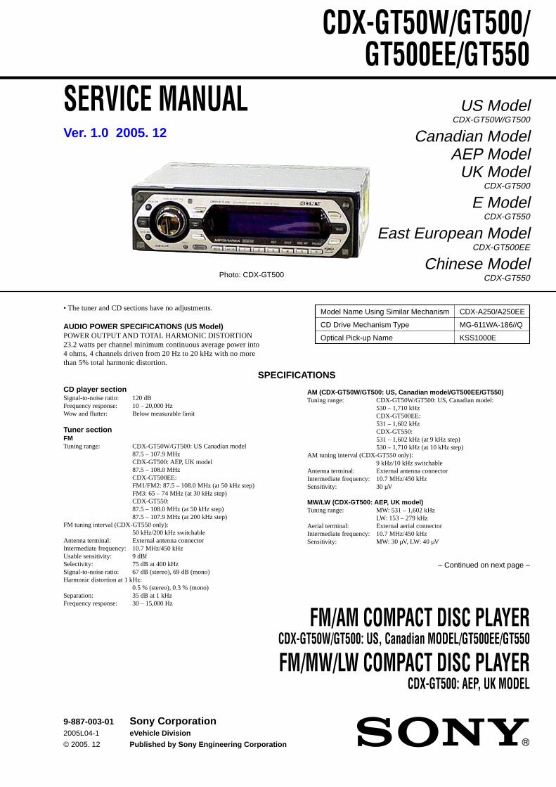
Photo: CDX-GT500
2
CDX-GT50W/GT500/GT500EE/GT550
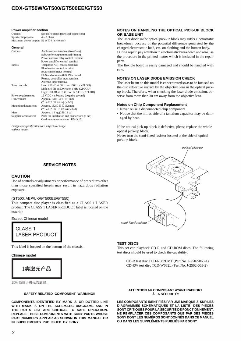
If the optical pick-up block is defective, please replace the wholeoptical pick-up block.Never turn the semi-fixed resistor located at the side of opticalpick-up block.
NOTES ON HANDLING THE OPTICAL PICK-UP BLOCKOR BASE UNITThe laser diode in the optical pick-up block may suffer electrostaticbreakdown because of the potential difference generated by thecharged electrostatic load, etc. on clothing and the human body.During repair, pay attention to electrostatic breakdown and also usethe procedure in the printed matter which is included in the repairparts.The flexible board is easily damaged and should be handled withcare.
NOTES ON LASER DIODE EMISSION CHECKThe laser beam on this model is concentrated so as to be focused onthe disc reflective surface by the objective lens in the optical pick-up block. Therefore, when checking the laser diode emission, ob-serve from more than 30 cm away from the objective lens.
Notes on Chip Component Replacement• Never reuse a disconnected chip component.• Notice that the minus side of a tantalum capacitor may be dam-
aged by heat.
SERVICE NOTES
This label is located on the bottom of the chassis.TEST DISCSThis set can playback CD-R and CD-ROM discs. The followingtest discs should be used to check the capability:
CD-R test disc TCD-R082LMT (Part No. J-2502-063-1)CD-RW test disc TCD-W082L (Part No. J-2502-063-2)
optical pick-up
semi-fixed resistor
CAUTIONUse of controls or adjustments or performance of procedures otherthan those specified herein may result in hazardous radiationexposure.
(GT500: AEP/UK/GT500EE/GT550)This compact disc player is classified as a CLASS 1 LASERproduct. The CLASS 1 LASER PRODUCT label is located on theexterior.
Power amplifier sectionOutputs: Speaker outputs (sure seal connectors)Speaker impedance: 4 – 8 ohmsMaximum power output: 52 W × 4 (at 4 ohms)
GeneralOutputs: Audio outputs terminal (front/rear)
Subwoofer output terminal (mono)Power antenna relay control terminalPower amplifier control terminal
Inputs: Telephone ATT control terminalIllumination control terminalBUS control input terminalBUS audio input/AUX IN terminalRemote controller input terminalAntenna input terminal
Tone controls: Low: ±10 dB at 60 Hz or 100 Hz (XPLOD)Mid: ±10 dB at 500 Hz or 1 kHz (XPLOD)High: ±10 dB at 10 kHz or 12.5 kHz (XPLOD)
Power requirements: 12 V DC car battery (negative ground)Dimensions: Approx. 178 × 50 × 181 mm
(7 1/8 × 2 × 7 1/4 in) (w/h/d)Mounting dimensions: Approx. 182 × 53 × 162 mm
(7 1/4 × 2 1/8 × 6 1/2 in) (w/h/d)Mass: Approx. 1.2 kg (2 lb 11 oz)Supplied accessories: Parts for installation and connections (1 set)
Card remote commander: RM-X151
Design and specifications are subject to changewithout notice.
SAFETY-RELATED COMPONENT WARNING!!
COMPONENTS IDENTIFIED BY MARK 0 OR DOTTED LINEWITH MARK 0 ON THE SCHEMATIC DIAGRAMS AND INTHE PARTS LIST ARE CRITICAL TO SAFE OPERATION.REPLACE THESE COMPONENTS WITH SONY PARTS WHOSEPART NUMBERS APPEAR AS SHOWN IN THIS MANUAL ORIN SUPPLEMENTS PUBLISHED BY SONY.
ATTENTION AU COMPOSANT AYANT RAPPORT À LA SÉCURITÉ!!
LES COMPOSANTS IDENTIFIÉS PAR UNE MARQUE 0 SUR LESDIAGRAMMES SCHÉMATIQUES ET LA LISTE DES PIÈCESSONT CRITIQUES POUR LA SÉCURITÉ DE FONCTIONNEMENT.NE REMPLACER CES COMPOSANTS QUE PAR DES PIÈCESSONY DONT LES NUMÉROS SONT DONNÉS DANS CE MANUELOU DANS LES SUPPLÉMENTS PUBLIÉS PAR SONY.
Except Chinese model
Chinese model
3
CDX-GT50W/GT500/GT500EE/GT550
z UNLEADED SOLDERBoards requiring use of unleaded solder are printed with the leadfree mark (LF) indicating the solder contains no lead.(Caution: Some printed circuit boards may not come printed withthe lead free mark due to their particular size.)
: LEAD FREE MARKUnleaded solder has the following characteristics.• Unleaded solder melts at a temperature about 40°C higher than
ordinary solder.Ordinary soldering irons can be used but the iron tip has to beapplied to the solder joint for a slightly longer time.Soldering irons using a temperature regulator should be set toabout 350°C.Caution: The printed pattern (copper foil) may peel away if theheated tip is applied for too long, so be careful!
• Strong viscosityUnleaded solder is more viscous (sticky, less prone to flow)than ordinary solder so use caution not to let solder bridgesoccur such as on IC pins, etc.
• Usable with ordinary solderIt is best to use only unleaded solder but unleaded solder mayalso be added to ordinary solder.
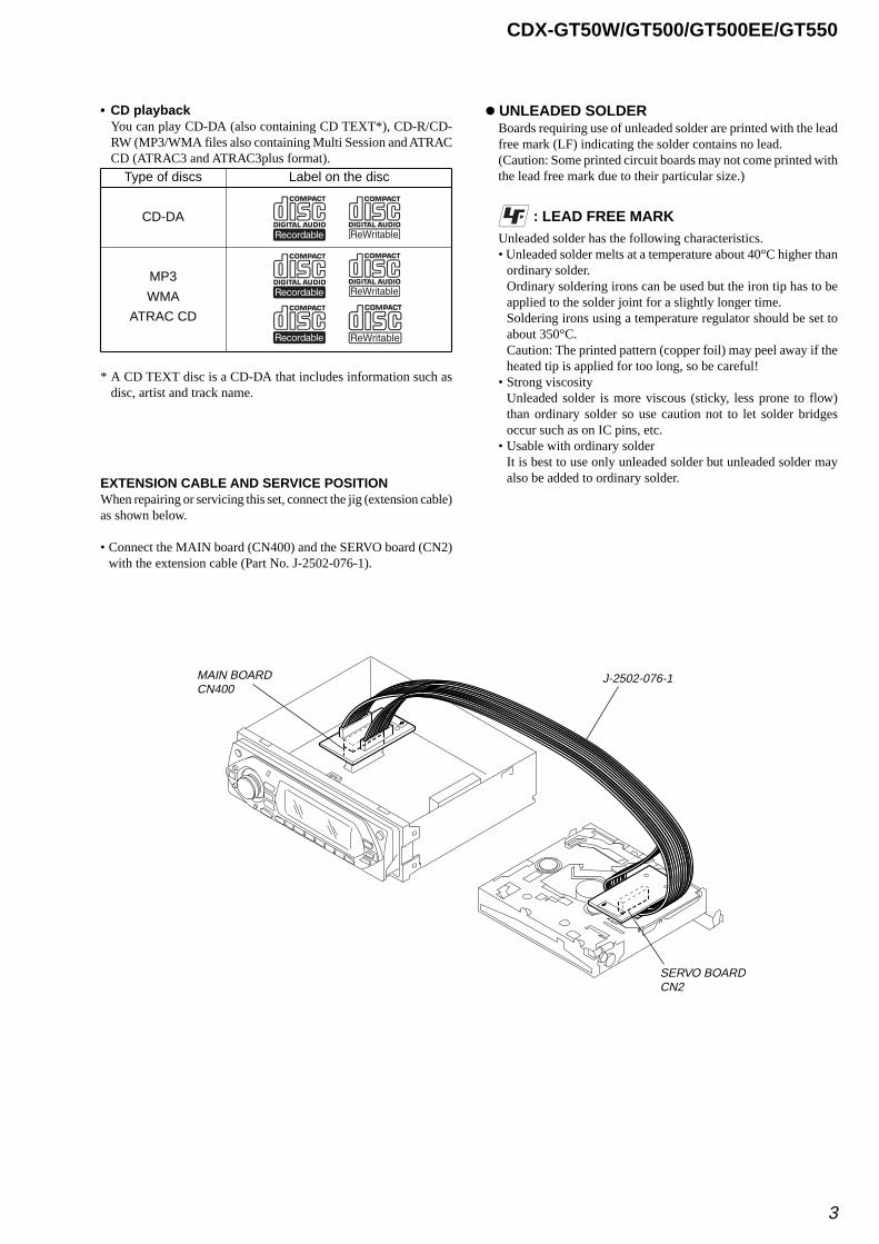
SERVO BOARDCN2
MAIN BOARDCN400
J-2502-076-1
EXTENSION CABLE AND SERVICE POSITIONWhen repairing or servicing this set, connect the jig (extension cable)as shown below.
• Connect the MAIN board (CN400) and the SERVO board (CN2)with the extension cable (Part No. J-2502-076-1).
• CD playbackYou can play CD-DA (also containing CD TEXT*), CD-R/CD-RW (MP3/WMA files also containing Multi Session and ATRACCD (ATRAC3 and ATRAC3plus format).
Type of discs Label on the disc
CD-DA
MP3
WMA
ATRAC CD
* A CD TEXT disc is a CD-DA that includes information such asdisc, artist and track name.
4
CDX-GT50W/GT500/GT500EE/GT550
TABLE OF CONTENTS
1. GENERALLocation of controls and basic operations ............................... 5Connections ............................................................................. 7
2. DISASSEMBLY2-1. Sub (FL) Panel Assy ......................................................... 122-2. CD Mechanism Block ....................................................... 122-3. Main Board ....................................................................... 132-4. Chassis (T) Sub Assy ........................................................ 132-5. Roller Arm Assy ................................................................ 142-6. Chassis (OP) Assy ............................................................. 142-7. Optical Pick-up ................................................................. 152-8. SL Motor Assy (M902) ..................................................... 152-9. LE Motor Assy (M903) ..................................................... 162-10. Servo Board ....................................................................... 16
3. DIAGRAMS3-1. Block Diagram – CD Section – ......................................... 173-2. Block Diagram – Main Section – ...................................... 183-3. Block Diagram – Display Section – .................................. 193-4. Circuit Boards Location .................................................... 203-5. Printed Wiring Boards – CD Mechanism Section – ......... 213-6. Schematic Diagram – CD Mechanism Section (1/2) – ..... 223-7. Schematic Diagram – CD Mechanism Section (2/2) – ..... 233-8. Printed Wiring Board – Main Section – ............................ 243-9. Schematic Diagram – Main Section (1/3) – ...................... 263-10. Schematic Diagram – Main Section (2/3) – ...................... 273-11. Schematic Diagram – Main Section (3/3) – ...................... 283-12. Printed Wiring Board – Sub Section – .............................. 293-13. Schematic Diagram – Sub Section – ................................. 303-14. Printed Wiring Board – Key Section – .............................. 313-15. Schematic Diagram – Key Section – ................................ 32
4. EXPLODED VIEWS4-1. Main Section ..................................................................... 404-2. Front Panel Section ........................................................... 414-3. CD Mechanism Section (1) (MG-611WA-186//Q) ........... 424-4. CD Mechanism Section (2) (MG-611WA-186//Q) ........... 434-5. CD Mechanism Section (3) (MG-611WA-186//Q) ........... 444-6. CD Mechanism Section (4) (MG-611WA-186//Q) ........... 45
5. ELECTRICAL PARTS LIST ........................................ 46
5
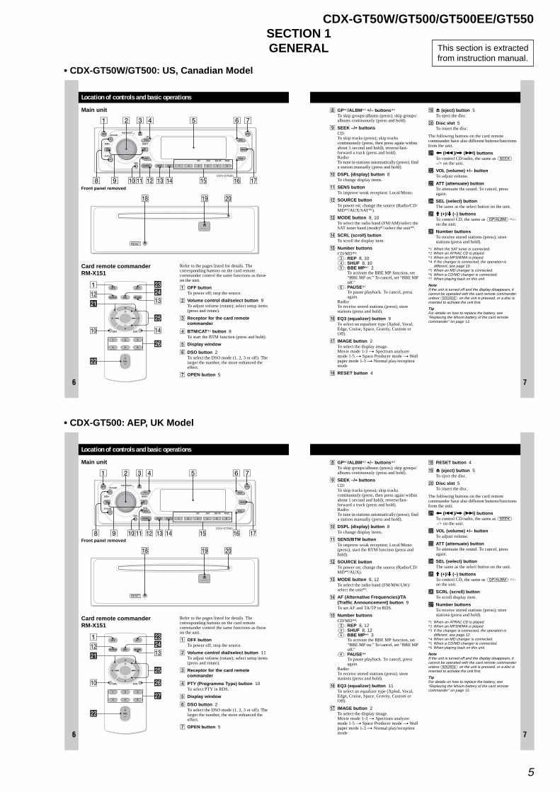
CDX-GT50W/GT500/GT500EE/GT550SECTION 1GENERAL This section is extracted
from instruction manual.
• CDX-GT50W/GT500: US, Canadian Model
• CDX-GT500: AEP, UK Model
6
Location of controls and basic operations
Main unit
Front panel removed
Card remote commander RM-X151
Refer to the pages listed for details. The corresponding buttons on the card remote commander control the same functions as those on the unit.
A OFF buttonTo power off; stop the source.
B Volume control dial/select button 9To adjust volume (rotate); select setup items (press and rotate).
C Receptor for the card remote commander
D BTM/CAT*1 button 8To start the BTM function (press and hold).
E Display window
F DSO button 2To select the DSO mode (1, 2, 3 or off). The larger the number, the more enhanced the effect.
G OPEN button 5
CDX-GT500
RESET
ql w;qk
7
H GP*2/ALBM*3 +/– buttons*4
To skip groups/albums (press); skip groups/albums continuously (press and hold).
I SEEK –/+ buttonsCD:To skip tracks (press); skip tracks continuously (press, then press again within about 1 second and hold); reverse/fast-forward a track (press and hold).Radio:To tune in stations automatically (press); find a station manually (press and hold).
J DSPL (display) button 8To change display items.
K SENS buttonTo improve weak reception: Local/Mono.
L SOURCE buttonTo power on; change the source (Radio/CD/MD*5/AUX/SAT*1).
M MODE button 8, 10To select the radio band (FM/AM)/select the SAT tuner band (mode)*1/select the unit*6.
N SCRL (scroll) buttonTo scroll the display item.
O Number buttonsCD/MD*5:(3): REP 8, 10(4): SHUF 8, 10(5): BBE MP*7 2
To activate the BBE MP function, set “BBE MP on.” To cancel, set “BBE MP off.”
(6): PAUSE*7
To pause playback. To cancel, press again.
Radio:To receive stored stations (press); store stations (press and hold).
P EQ3 (equalizer) button 9To select an equalizer type (Xplod, Vocal, Edge, Cruise, Space, Gravity, Custom or Off).
Q IMAGE button 2To select the display image.Movie mode 1-3 t Spectrum analyzer mode 1-5 t Space Producer mode t Wall paper mode 1-3 t Normal play/reception mode
R RESET button 4
S Z (eject) button 5To eject the disc.
T Disc slot 5To insert the disc.
The following buttons on the card remote commander have also different buttons/functions from the unit.
wa < (.)/, (>) buttonsTo control CD/radio, the same as (SEEK) –/+ on the unit.
ws VOL (volume) +/– buttonTo adjust volume.
wd ATT (attenuate) buttonTo attenuate the sound. To cancel, press again.
wf SEL (select) buttonThe same as the select button on the unit.
wg M (+)/m (–) buttonsTo control CD, the same as (GP/ALBM) +/– on the unit.
wh Number buttonsTo receive stored stations (press); store stations (press and hold).
*1 When the SAT tuner is connected.*2 When an ATRAC CD is played.*3 When an MP3/WMA is played. *4 If the changer is connected, the operation is
different, see page 10.*5 When an MD changer is connected.*6 When a CD/MD changer is connected.*7 When playing back on this unit.
NoteIf the unit is turned off and the display disappears, it cannot be operated with the card remote commander unless (SOURCE) on the unit is pressed, or a disc is inserted to activate the unit first.
TipFor details on how to replace the battery, see “Replacing the lithium battery of the card remote commander” on page 13.
6
Location of controls and basic operations
Main unit
Front panel removed
Card remote commander RM-X151
Refer to the pages listed for details. The corresponding buttons on the card remote commander control the same functions as those on the unit.
A OFF buttonTo power off; stop the source.
B Volume control dial/select button 11To adjust volume (rotate); select setup items (press and rotate).
C Receptor for the card remote commander
D PTY (Programme Type) button 10To select PTY in RDS.
E Display window
F DSO button 2To select the DSO mode (1, 2, 3 or off). The larger the number, the more enhanced the effect.
G OPEN button 5
CDX-GT500
RESET
ql w;qk
7
H GP*1/ALBM*2 +/– buttons*3
To skip groups/albums (press); skip groups/albums continuously (press and hold).
I SEEK –/+ buttonsCD:To skip tracks (press); skip tracks continuously (press, then press again within about 1 second and hold); reverse/fast-forward a track (press and hold).Radio:To tune in stations automatically (press); find a station manually (press and hold).
J DSPL (display) button 8To change display items.
K SENS/BTM buttonTo improve weak reception: Local/Mono (press); start the BTM function (press and hold).
L SOURCE buttonTo power on; change the source (Radio/CD/MD*4/AUX).
M MODE button 8, 12To select the radio band (FM/MW/LW)/select the unit*5.
N AF (Alternative Frequencies)/TA (Traffic Announcement) button 9To set AF and TA/TP in RDS.
O Number buttonsCD/MD*4:(3): REP 8, 12(4): SHUF 8, 12(5): BBE MP*6 3
To activate the BBE MP function, set “BBE MP on.” To cancel, set “BBE MP off.”
(6): PAUSE*6
To pause playback. To cancel, press again.
Radio:To receive stored stations (press); store stations (press and hold).
P EQ3 (equalizer) button 11To select an equalizer type (Xplod, Vocal, Edge, Cruise, Space, Gravity, Custom or Off).
Q IMAGE button 2To select the display image.Movie mode 1-3 t Spectrum analyzer mode 1-5 t Space Producer mode t Wall paper mode 1-3 t Normal play/reception mode
R RESET button 4
S Z (eject) button 5To eject the disc.
T Disc slot 5To insert the disc.
The following buttons on the card remote commander have also different buttons/functions from the unit.
wa < (.)/, (>) buttonsTo control CD/radio, the same as (SEEK) –/+ on the unit.
ws VOL (volume) +/– buttonTo adjust volume.
wd ATT (attenuate) buttonTo attenuate the sound. To cancel, press again.
wf SEL (select) buttonThe same as the select button on the unit.
wg M (+)/m (–) buttonsTo control CD, the same as (GP/ALBM) +/– on the unit.
wh SCRL (scroll) buttonTo scroll display item.
wj Number buttonsTo receive stored stations (press); store stations (press and hold).
*1 When an ATRAC CD is played.*2 When an MP3/WMA is played. *3 If the changer is connected, the operation is
different, see page 12.*4 When an MD changer is connected.*5 When a CD/MD changer is connected.*6 When playing back on this unit.
NoteIf the unit is turned off and the display disappears, it cannot be operated with the card remote commander unless (SOURCE) on the unit is pressed, or a disc is inserted to activate the unit first.
TipFor details on how to replace the battery, see “Replacing the lithium battery of the card remote commander” on page 15.
6
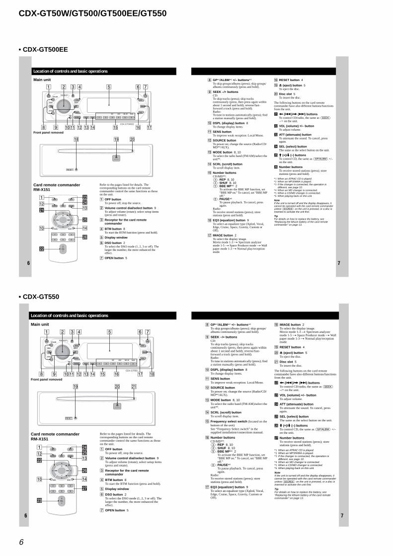
CDX-GT50W/GT500/GT500EE/GT550
• CDX-GT500EE
• CDX-GT550
6
Location of controls and basic operations
Main unit
Front panel removed
Card remote commander RM-X151
Refer to the pages listed for details. The corresponding buttons on the card remote commander control the same functions as those on the unit.
A OFF buttonTo power off; stop the source.
B Volume control dial/select button 9To adjust volume (rotate); select setup items (press and rotate).
C Receptor for the card remote commander
D BTM button 8To start the BTM function (press and hold).
E Display window
F DSO button 2To select the DSO mode (1, 2, 3 or off). The larger the number, the more enhanced the effect.
G OPEN button 5
CDX-GT550
RESET
ql waw;
7
H GP*1/ALBM*2 +/– buttons*3
To skip groups/albums (press); skip groups/albums continuously (press and hold).
I SEEK –/+ buttonsCD:To skip tracks (press); skip tracks continuously (press, then press again within about 1 second and hold); reverse/fast-forward a track (press and hold).Radio:To tune in stations automatically (press); find a station manually (press and hold).
J DSPL (display) button 8To change display items.
K SENS buttonTo improve weak reception: Local/Mono.
L SOURCE buttonTo power on; change the source (Radio/CD/MD*4/AUX).
M MODE button 8, 10To select the radio band (FM/AM)/select the unit*5.
N SCRL (scroll) buttonTo scroll display item.
O Frequency select switch (located on the bottom of the unit)See “Frequency Select switch” in the supplied installation/connections manual.
P Number buttonsCD/MD*4:(3): REP 8, 10(4): SHUF 8, 10(5): BBE MP*6 2
To activate the BBE MP function, set “BBE MP on.” To cancel, set “BBE MP off.”
(6): PAUSE*6
To pause playback. To cancel, press again.
Radio:To receive stored stations (press); store stations (press and hold).
Q EQ3 (equalizer) button 9To select an equalizer type (Xplod, Vocal, Edge, Cruise, Space, Gravity, Custom or Off).
R IMAGE button 2To select the display image.Movie mode 1-3 t Spectrum analyzer mode 1-5 t Space Producer mode t Wall paper mode 1-3 t Normal play/reception mode
S RESET button 4
T Z (eject) button 5To eject the disc.
U Disc slot 5To insert the disc.
The following buttons on the card remote commander have also different buttons/functions from the unit.
ws < (.)/, (>) buttonsTo control CD/radio, the same as (SEEK) –/+ on the unit.
wd VOL (volume) +/– buttonTo adjust volume.
wf ATT (attenuate) buttonTo attenuate the sound. To cancel, press again.
wg SEL (select) buttonThe same as the select button on the unit.
wh M (+)/m (–) buttonsTo control CD, the same as (GP/ALBM) +/– on the unit.
wj Number buttonsTo receive stored stations (press); store stations (press and hold).
*1 When an ATRAC CD is played.*2 When an MP3/WMA is played. *3 If the changer is connected, the operation is
different, see page 10.*4 When an MD changer is connected.*5 When a CD/MD changer is connected.*6 When playing back on this unit.
NoteIf the unit is turned off and the display disappears, it cannot be operated with the card remote commander unless (SOURCE) on the unit is pressed, or a disc is inserted to activate the unit first.
TipFor details on how to replace the battery, see “Replacing the lithium battery of the card remote commander” on page 13.
6
Location of controls and basic operations
Main unit
Front panel removed
Card remote commander RM-X151
Refer to the pages listed for details. The corresponding buttons on the card remote commander control the same functions as those on the unit.
A OFF buttonTo power off; stop the source.
B Volume control dial/select button 9To adjust volume (rotate); select setup items (press and rotate).
C Receptor for the card remote commander
D BTM button 8To start the BTM function (press and hold).
E Display window
F DSO button 2To select the DSO mode (1, 2, 3 or off). The larger the number, the more enhanced the effect.
G OPEN button 5
CDX-GT500EE
RESET
ql w;qk
7
H GP*1/ALBM*2 +/– buttons*3
To skip groups/albums (press); skip groups/albums continuously (press and hold).
I SEEK –/+ buttonsCD:To skip tracks (press); skip tracks continuously (press, then press again within about 1 second and hold); reverse/fast-forward a track (press and hold).Radio:To tune in stations automatically (press); find a station manually (press and hold).
J DSPL (display) button 8To change display items.
K SENS buttonTo improve weak reception: Local/Mono.
L SOURCE buttonTo power on; change the source (Radio/CD/MD*4/AUX).
M MODE button 8, 10To select the radio band (FM/AM)/select the unit*5.
N SCRL (scroll) buttonTo scroll display item.
O Number buttonsCD/MD*4:(3): REP 8, 10(4): SHUF 8, 10(5): BBE MP*6 2
To activate the BBE MP function, set “BBE MP on.” To cancel, set “BBE MP off.”
(6): PAUSE*6
To pause playback. To cancel, press again.
Radio:To receive stored stations (press); store stations (press and hold).
P EQ3 (equalizer) button 9To select an equalizer type (Xplod, Vocal, Edge, Cruise, Space, Gravity, Custom or Off).
Q IMAGE button 2To select the display image.Movie mode 1-3 t Spectrum analyzer mode 1-5 t Space Producer mode t Wall paper mode 1-3 t Normal play/reception mode
R RESET button 4
S Z (eject) button 5To eject the disc.
T Disc slot 5To insert the disc.
The following buttons on the card remote commander have also different buttons/functions from the unit.
wa < (.)/, (>) buttonsTo control CD/radio, the same as (SEEK) –/+ on the unit.
ws VOL (volume) +/– buttonTo adjust volume.
wd ATT (attenuate) buttonTo attenuate the sound. To cancel, press again.
wf SEL (select) buttonThe same as the select button on the unit.
wg M (+)/m (–) buttonsTo control CD, the same as (GP/ALBM) +/– on the unit.
wh Number buttonsTo receive stored stations (press); store stations (press and hold).
*1 When an ATRAC CD is played.*2 When an MP3/WMA is played. *3 If the changer is connected, the operation is
different, see page 10.*4 When an MD changer is connected.*5 When a CD/MD changer is connected.*6 When playing back on this unit.
NoteIf the unit is turned off and the display disappears, it cannot be operated with the card remote commander unless (SOURCE) on the unit is pressed, or a disc is inserted to activate the unit first.
TipFor details on how to replace the battery, see “Replacing the lithium battery of the card remote commander” on page 13.
7
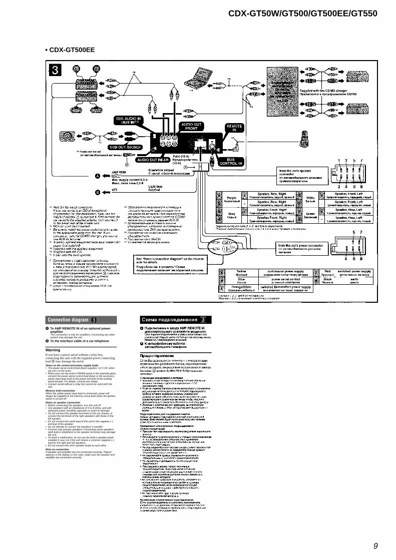
CDX-GT50W/GT500/GT500EE/GT550
• CONNECTIONS• CDX-GT50W/GT500: US, Canadian Model
L
R
AUDIOOUT
REAR
AUDIOOUT
FRONT
BUSAUDIO
IN
2
4
5
6
7
1
3
AUDIO OUTFRONT
BUS AUDIO IN /AUX IN*2
BUSCONTROL IN
REMOTEIN
AUDIO OUTREAR
SUB OUT (MONO)
Schéma de raccordement
1 À un point métallique de la voitureBranchez d’abord le fi l de masse noir et, ensuite, les fi ls d’entrée d’alimentation rayé orange/blanc, jaune, et rouge.
2 Vers le câble de commande d’antenne électrique ou le câble d’alimentation de l’amplifi cateur d’antenneRemarques• Il n’est pas nécessaire de raccorder ce câble s’il n’y a pas
d’antenne électrique ni d’amplifi cateur d’antenne, ou avec une antenne télescopique manuelle.
• Si votre voiture est équipée d’une antenne FM/AM intégrée dans la vitre arrière/latérale, voir « Remarques sur les câbles de commande et d’alimentation ».
3 Au niveau de AMP REMOTE IN de l’amplifi cateur de puissance en optionCe raccordement s’applique uniquement aux amplifi cateurs. Le branchement de tout autre système risque d’endommager l’appareil.
4 Vers le cordon de liaison d’un téléphone de voiture
5 Vers le connecteur du signal d’éclairage de la voitureRaccordez d’abord le câble de mise à la masse noir à un point métallique du véhicule.
6 À la borne +12 V qui est alimentée quand la clé de contact est sur la position accessoiresRemarques• S’il n’y a pas de position accessoires, raccordez la borne
d’alimentation (batterie) +12 V qui est alimentée en permanence.Raccordez d’abord le câble de mise à la masse noir à un point métallique du véhicule.
• Si votre voiture est équipée d’une antenne FM/AM intégrée dans la vitre arrière/latérale, voir « Remarques sur les câbles de commande et d’alimentation ».
7 À la borne +12 V qui est alimentée en permanenceRaccordez d’abord le câble de mise à la masse noir à un point métallique du véhicule.
Connection diagram
1 To a metal surface of the carFirst connect the black ground lead, then connect the orange/white striped, yellow, and red power input leads.
2 To the power antenna control lead or power supply lead of antenna booster amplifi erNotes• It is not necessary to connect this lead if there is no power
antenna or antenna booster, or with a manually-operated telescopic antenna.
• When your car has a built-in FM/AM antenna in the rear/side glass, see “Notes on the control and power supply leads.”
3 To AMP REMOTE IN of an optional power amplifi erThis connection is only for amplifi ers. Connecting any other system may damage the unit.
4 To the interface cable of a car telephone5 To a car’s illumination signal
Be sure to connect the black ground lead to a metal surface of the car fi rst.
6 To the +12 V power terminal which is energized in the accessory position of the ignition key switchNotes• If there is no accessory position, connect to the +12 V
power (battery) terminal which is energized at all times. Be sure to connect the black ground lead to a metal
surface of the car fi rst.• When your car has a built-in FM/AM antenna in the rear/
side glass, see “Notes on the control and power supply leads.”
7 To the +12 V power terminal which is energized at all timesBe sure to connect the black ground lead to a metal surface of the car fi rst.
Remarques sur les câbles de commande et d’alimentation• Le câble de commande d’antenne électrique (bleu) fournit une
alimentation de + 12 V CC lorsque vous mettez la radio sous tension.
• Lorsque votre voiture est équipée d’une antenne FM/AM intégrée dans la vitre arrière/latérale, raccordez le câble de commande d’antenne (bleu) ou l’entrée d’alimentation des accessoires (rouge) à la borne d’alimentation de l’amplifi cateur d’antenne existant. Pour plus de détails, consultez votre détaillant.
• Une antenne électrique sans boîtier de relais ne peut pas être utilisée avec cet appareil.
Raccordement pour la conservation de la mémoireLorsque le câble d’entrée d’alimentation jaune est raccordé, le circuit de la mémoire est alimenté en permanence même si la clé de contact est sur la position d’arrêt.
Remarques sur le raccordement des haut-parleurs• Avant de raccorder les haut-parleurs, mettez l’appareil hors
tension.• Utilisez des haut-parleurs ayant une impédance de 4 à 8 ohms
avec une capacité électrique adéquate pour éviter de les endommager.
• Ne raccordez pas les bornes du système de haut-parleurs au châssis de la voiture et ne raccordez pas les bornes des haut-parleurs droit à celles du haut-parleur gauche.
• Ne raccordez pas le câble de mise à la masse de cet appareil à la borne négative (–) du haut-parleur.
• N’essayez pas de raccorder les haut-parleurs en parallèle.• Raccordez uniquement des haut-parleurs passifs. Le
raccordement de haut-parleurs actifs (avec amplifi cateurs intégrés) aux bornes des haut-parleurs peut endommager l’appareil.
• Pour éviter tout problème de fonctionnement, n’utilisez pas les câbles des haut-parleurs intégrés installés dans votre voiture si l’appareil partage un câble négatif commun (–) pour les haut-parleurs droit et gauche.
• Ne raccordez pas entre eux les cordons des haut-parleurs de l’appareil.
Remarque sur le raccordementSi les haut-parleurs et l’amplifi cateur ne sont pas raccordés correctement, le message « Failure » s’affi che. Dans ce cas, assurez-vous que les haut-parleurs et l’amplifi cateur sont bien raccordés.
Notes on the control and power supply leads• The power antenna control lead (blue) supplies +12 V DC
when you turn on the tuner.• When your car has built-in FM/AM antenna in the rear/side
glass, connect the power antenna control lead (blue) or the accessory power input lead (red) to the power terminal of the existing antenna booster. For details, consult your dealer.
• A power antenna without a relay box cannot be used with this unit.
Memory hold connectionWhen the yellow power input lead is connected, power will always be supplied to the memory circuit even when the ignition switch is turned off.
Notes on speaker connection• Before connecting the speakers, turn the unit off.• Use speakers with an impedance of 4 to 8 ohms, and with
adequate power handling capacities to avoid its damage.• Do not connect the speaker terminals to the car chassis, or
connect the terminals of the right speakers with those of the left speaker.
• Do not connect the ground lead of this unit to the negative (–) terminal of the speaker.
• Do not attempt to connect the speakers in parallel.• Connect only passive speakers. Connecting active speakers
(with built-in amplifi ers) to the speaker terminals may damage the unit.
• To avoid a malfunction, do not use the built-in speaker leads installed in your car if the unit shares a common negative (–) lead for the right and left speakers.
• Do not connect the unit’s speaker leads to each other.
Note on connectionIf speaker and amplifi er are not connected correctly, “Failure” appears in the display. In this case, make sure the speaker and amplifi er are connected correctly.
AMP REM
Max. supply current 0.3 ACourant max. fourni 0,3 A
Fuse (10 A)Fusible (10 A)
Blue/white stripedRayé bleu/blanc
ANT REM
*1
RedRouge
YellowJaune
BlackNoir
BlueBleu
WhiteBlanc
GreenVert
PurpleMauve
White/black stripedRayé blanc/noir
Gray/black stripedRayé gris/noir
Green/black stripedRayé vert/noir
GrayGris
LeftGauche
RightDroit
LeftGauche
RightDroit
Purple/black stripedRayé mauve/noir
*1
Source selector(not supplied)
Sélecteur de source(non fourni)
XA-C30
Supplied with the CD/MD changerFourni avec le changeur de CD/MD
*6
Max. supply current 0.1 ACourant max. fourni 0,1 A
ILLUMINATION
Light blueBleu ciel
Orange/white stripedRayé orange/blanc
ATT
from car antennaà partir de l’antenne de la voiture
*1 RCA pin cord (not supplied)*2 Be sure to match the color-
coded cord for audio to the appropriate jacks from the unit. If you connect an optional CD/MD changer, you cannot use AUX IN terminal.
*3 Auxiliary optional equipment such as portable DVD player (not supplied)
*4 Supplied with the auxiliary equipment
*5 Supplied with XA-C30*6 Insert with the cord upwards.
*1 Cordon à broche RCA (non fourni)
*2 Veillez à faire correspondre le code de couleur du cordon audio à celui des fi ches correspondantes de l’appareil. Si vous raccordez un changeur de CD/MD en option, vous ne pouvez pas utiliser la borne AUX IN.
*3 Appareil auxiliaire en option, par exemple un lecteur de DVD portable (non fourni)
*4 Fourni avec l’appareil auxiliaire*5 Fourni avec le XA-C30*6 Insérez avec le câble vers le
haut.
*5
*4
*3
2
8
CDX-GT50W/GT500/GT500EE/GT550
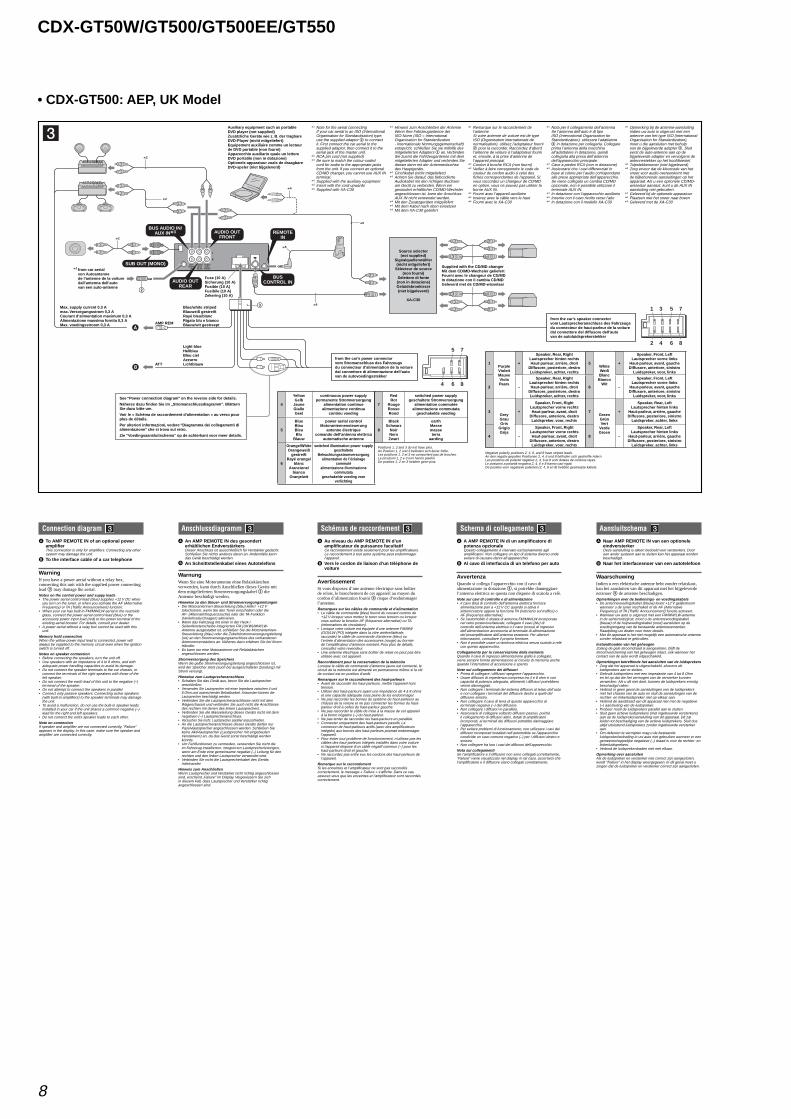
• CDX-GT500: AEP, UK Model
L
R
AUDIOOUT
REAR
AUDIOOUT
FRONT
BUSAUDIO
IN
5 7
4 8
1 3 5 7
2 4 6 8
A
B
6
AUDIO OUTREAR
BUSCONTROL IN
REMOTEIN
AUDIO OUTFRONT
BUS AUDIO IN/ AUX IN*3
SUB OUT (MONO)Supplied with the CD/MD changerMit dem CD/MD-Wechsler geliefertFourni avec le changeur de CD/MDIn dotazione con il cambia CD/MDGeleverd met de CD/MD-wisselaar
*1 from car aerial von Autoantenne de l’antenne de la voiture dall’antenna dell’auto van een auto-antenne
Fuse (10 A)Sicherung (10 A)Fusible (10 A)Fusibile (10 A)Zekering (10 A)
AMP REM
Light blueHellblauBleu cielAzzurroLichtblauw
Blue/white stripedBlauweiß gestreiftRayé bleu/blancRigato blu e biancoBlauw/wit gestreept
from the car’s power connectorvom Stromanschluss des Fahrzeugsdu connecteur d’alimentation de la voituredal connettore di alimentazione dell’autovan de autovoedingsstekker
ATT
See “Power connection diagram” on the reverse side for details.
Näheres dazu fi nden Sie im „Stromanschlussdiagramm“. Blättern Sie dazu bitte um.
Voir le « Schéma de raccordement d’alimentation » au verso pour plus de détails.
Per ulteriori informazioni, vedere “Diagramma dei collegamenti di alimentazione” che si trova sul retro.
Zie "Voedingsaansluitschema" op de achterkant voor meer details.
Max. supply current 0.3 Amax. Versorgungsstrom 0,3 ACourant d’alimentation maximum 0,3 AAlimentazione massima fornita 0,3 AMax. voedingsstroom 0,3 A
*2
*4
Negative polarity positions 2, 4, 6, and 8 have striped leads.An den negativ gepolten Positionen 2, 4, 6 und 8 befi nden sich gestreifte Adern.Les positions de polarité négative 2, 4, 6 et 8 sont dotées de cordons rayés.Le posizioni a polarità negativa 2, 4, 6 e 8 hanno cavi rigati.De posities voor negatieve polariteit (2, 4, 6 en 8) hebben gestreepte kabels.
1PurpleViolettMauveViolaPaars
+
Speaker, Rear, RightLautsprecher hinten rechtsHaut-parleur, arrière, droit
Diffusore, posteriore, destroLuidspreker, achter, rechts
5WhiteWeißBlanc
BiancoWit
+
Speaker, Front, LeftLautsprecher vorne links
Haut-parleur, avant, gaucheDiffusore, anteriore, sinistro
Luidspreker, voor, links
2 –
Speaker, Rear, RightLautsprecher hinten rechtsHaut-parleur, arrière, droit
Diffusore, posteriore, destroLuidspreker, achter, rechts
6 –
Speaker, Front, LeftLautsprecher vorne links
Haut-parleur, avant, gaucheDiffusore, anteriore, sinistro
Luidspreker, voor, links
3GreyGrauGris
GrigioGrijs
+
Speaker, Front, RightLautsprecher vorne rechtsHaut-parleur, avant, droit
Diffusore, anteriore, destroLuidspreker, voor, rechts
7GreenGrünVert
VerdeGroen
+
Speaker, Rear, LeftLautsprecher hinten links
Haut-parleur, arrière, gaucheDiffusore, posteriore, sinistro
Luidspreker, achter, links
4 –
Speaker, Front, RightLautsprecher vorne rechtsHaut-parleur, avant, droit
Diffusore, anteriore, destroLuidspreker, voor, rechts
8 –
Speaker, Rear, LeftLautsprecher hinten links
Haut-parleur, arrière, gaucheDiffusore, posteriore, sinistro
Luidspreker, achter, links
*2
Source selector(not supplied)
Signalquellenwähler(nicht mitgeliefert)
Sélecteur de source(non fourni)
Selettore di fonte(non in dotazione)Geluidsbronkiezer(niet bijgeleverd)
XA-C30
from the car’s speaker connectorvom Lautsprecheranschluss des Fahrzeugsdu connecteur de haut-parleur de la voituredal connettore del diffusore dell’autovan de autoluidsprekerstekker
Positions 1, 2 and 3 do not have pins.An Position 1, 2 und 3 befi nden sich keine Stifte.Les positions 1, 2 et 3 ne comportent pas de broches.Le posizioni 1, 2 e 3 non hanno piedini.De posities 1, 2 en 3 hebben geen pins.
4
YellowGelb
JauneGialloGeel
continuous power supplypermanente Stromversorgung
alimentation continuealimentazione continua
continu voeding
5
BlueBlauBleuBlu
Blauw
power aerial controlMotorantennensteuerung
antenne électriquecomando dell’antenna elettrica
automatische antenne
6
Orange/WhiteOrangeweiß
gestreiftRayé orange/
blancArancione/
biancoOranje/wit
switched illumination power supplygeschaltete
Beleuchtungsstromversorgungalimentation de l’éclairage
commutéalimentazione illuminazione
commutatageschakelde voeding voor
verlichting
7
RedRot
RougeRossoRood
switched power supplygeschaltete Stromversorgung
alimentation commutéealimentazione commutata
geschakelde voeding
8
BlackSchwarz
NoirNeroZwart
earthMassemasseterra
aarding
*2
*6
*5
*6
*1 Note for the aerial connectingIf your car aerial is an ISO (International Organisation for Standardisation) type, use the supplied adaptor 2 to connect it. First connect the car aerial to the supplied adaptor, then connect it to the aerial jack of the master unit.
*2 RCA pin cord (not supplied)*3 Be sure to match the colour-coded
cord for audio to the appropriate jacks from the unit. If you connect an optional CD/MD changer, you cannot use AUX IN terminal.
*4 Supplied with the auxiliary equipment*5 Insert with the cord upwards*6 Supplied with XA-C30
*1 Hinweis zum Anschließen der AntenneWenn Ihre Fahrzeugantenne der ISO-Norm (ISO = International Organization for Standardization - Internationale Normungsgemeinschaft) entspricht, schließen Sie sie mithilfe des mitgelieferten Adapters 2 an. Verbinden Sie zuerst die Fahrzeugantenne mit dem mitgelieferten Adapter und verbinden Sie diesen dann mit der Antennenbuchse des Hauptgeräts.
*2 Cinchkabel (nicht mitgeliefert)*3 Achten Sie darauf, das farbcodierte
Audiokabel mit den richtigen Buchsen am Gerät zu verbinden. Wenn ein gesondert erhältlicher CD/MD-Wechsler angeschlossen ist, kann der Anschluss AUX IN nicht verwendet werden.
*4 Mit den Zusatzgeräten mitgeliefert*5 Mit dem Kabel nach oben einsetzen*6 Mit dem XA-C30 geliefert
*1 Remarque sur le raccordement de l’antenneSi votre antenne de voiture est de type ISO (Organisation internationale de normalisation), utilisez l’adaptateur fourni
pour la r2 accorder. Raccordez d’abord l’antenne de voiture à l’adaptateur fourni et, ensuite, à la prise d’antenne de l’appareil principal.
*2 Cordon à broche RCA (non fourni)*3 Veillez à faire correspondre le code de
couleur du cordon audio à celui des fi ches correspondantes de l’appareil. Si vous raccordez un changeur de CD/MD en option, vous ne pouvez pas utiliser la borne AUX IN.
*4 Fourni avec l’appareil auxiliaire*5 Insérez avec le câble vers le haut*6 Fourni avec le XA-C30
*1 Opmerking bij de antenne-aansluitingIndien uw auto is uitgerust met een antenne van het type ISO (International Organisation for Standardization), moet u die aansluiten met behulp van de bijgeleverde adapter 2. Sluit eerst de auto-antenne aan op de bijgeleverde adapter en vervolgens de antennestekker op het hoofdtoestel.
*2 Tulpstekkersnoer (niet bijgeleverd)*3 Zorg ervoor dat de kleurcode van het
snoer voor audio overeenkomt met de bijbehorende aansluitingen op het apparaat. Als u een optionele CD/MD-wisselaar aansluit, kunt u de AUX IN aansluiting niet gebruiken.
*4 Geleverd bij de optionele apparatuur*5 Plaatsen met het snoer naar boven*6 Geleverd met de XA-C30
Auxiliary equipment such as portable DVD player (not supplied)Zusätzliche Geräte wie z. B. der tragbare DVD-Player (nicht mitgeliefert)Equipement auxiliaire comme un lecteur de DVD portable (non fourni)Apparecchio ausiliario quale un lettore DVD portatile (non in dotazione)Optionele apparatuur zoals de draagbare DVD-speler (niet bijgeleverd)
*1 Nota per il collegamento dell’antennaSe l’antenna dell’auto è di tipo ISO (International Organization for Standardization), utilizzare l’adattatore
in dotazione per collegar2 la. Collegare prima l’antenna della macchina all’adattatore in dotazione, quindi collegarla alla presa dell’antenna dell’apparecchio principale.
*2 Cavo a piedini RCA (non in dotazione)*3 Assicurarsi che i cavi differenziati in
base al colore per l’audio corrispondano alle prese appropriate dell’apparecchio. Se viene collegato un cambia CD/MD opzionale, non è possibile utilizzare il terminale AUX IN.
*4 In dotazione con l’apparecchio ausiliario*5 Inserire con il cavo rivolto verso l’alto*6 In dotazione con il modello XA-C30
2
3
Aansluitschema
A Naar AMP REMOTE IN van een optionele eindversterkerDeze aansluiting is alleen bedoeld voor versterkers. Door een ander systeem aan te sluiten kan het apparaat worden beschadigd.
B Naar het interfacesnoer van een autotelefoon
WaarschuwingIndien u een elektrische antenne hebt zonder relaiskast, kan het aansluiten van dit apparaat met het bijgeleverde netsnoer 3 de antenne beschadigen.Opmerkingen over de bedienings- en voedingskabels• De antennevoedingskabel (blauw) levert +12 V gelijkstroom
wanneer u de tuner inschakelt of de AF (Alternative Frequency) of TA (Traffi c Announcement) functie activeert.
• Wanneer uw auto is uitgerust met een FM/MW/LW-antenne in de achterruit/zijruit, moet u de antennevoedingskabel (blauw) of de hulpvoedingskabel (rood) aansluiten op de voedingsingang van de bestaande antenneversterker. Raadpleeg uw dealer voor meer details.
• Met dit apparaat is het niet mogelijk een automatische antenne zonder relaiskast te gebruiken.
Instandhouden van het geheugenZolang de gele stroomdraad is aangesloten, blijft de stroomvoorziening van het geheugen intact, ook wanneer het contact van de auto wordt uitgeschakeld.
Opmerkingen betreffende het aansluiten van de luidsprekers• Zorg dat het apparaat is uitgeschakeld, alvorens de
luidsprekers aan te sluiten.• Gebruik luidsprekers met een impedantie van 4 tot 8 Ohm
en let op dat die het vermogen van de versterker kunnen verwerken. Als u dit niet doet, kunnen de luidsprekers ernstig beschadigd raken.
• Verbind in geen geval de aansluitingen van de luidsprekers met het chassis van de auto en sluit de aansluitingen van de rechter- en linkerluidspreker niet op elkaar aan.
• Verbind de aarddraad van dit apparaat niet met de negatieve (–) aansluiting van de luidspreker.
• Probeer nooit de luidsprekers parallel aan te sluiten.• Sluit geen actieve luidsprekers (met ingebouwde versterkers)
aan op de luidsprekeraansluiting van dit apparaat. Dit zal leiden tot beschadiging van de actieve luidsprekers. Sluit dus altijd uitsluitend luidsprekers zonder ingebouwde versterker aan.
• Om defecten te vermijden mag u de bestaande luidsprekerbedrading in uw auto niet gebruiken wanneer er een gemeenschappelijke negatieve (–) draad is voor de rechter- en linkerluidsprekers.
• Verbind de luidsprekerdraden niet met elkaar.
Opmerking over aansluitenAls de luidspreker en versterker niet correct zijn aangesloten, wordt "Failure" in het display weergegeven. In dit geval moet u zorgen dat de luidspreker en versterker correct zijn aangesloten.
Schémas de raccordement
A Au niveau du AMP REMOTE IN d’un amplifi cateur de puissance facultatifCe raccordement existe seulement pour les amplifi cateurs. Le raccordement à tout autre système peut endommager l’appareil.
B Vers le cordon de liaison d’un téléphone de voiture
AvertissementSi vous disposez d’une antenne électrique sans boîtier de relais, le branchement de cet appareil au moyen du cordon d’alimentation fourni 3 risque d’endommager l’antenne.Remarques sur les câbles de commande et d’alimentation• Le câble de commande (bleu) fournit du courant continu de
+12 V lorsque vous mettez le tuner sous tension ou lorsque vous activez la fonction AF (fréquence alternative) ou TA (informations de circulation).
• Lorsque votre voiture est équipée d’une antenne FM/MW (GO)/LW (PO) intégrée dans la vitre arrière/latérale, raccordez le câble de commande d’antenne (bleu) ou l’entrée d’alimentation des accessoires (rouge) au bornier de l’amplifi cateur d’antenne existant. Pour plus de détails, consultez votre revendeur.
• Une antenne électrique sans boîtier de relais ne peut pas être utilisée avec cet appareil.
Raccordement pour la conservation de la mémoireLorsque le câble de commande d’antenne jaune est connecté, le circuit de la mémoire est alimenté en permanence même si la clé de contact est en position d’arrêt.
Remarques sur le raccordement des haut-parleurs• Avant de raccorder les haut-parleurs, mettre l’appareil hors
tension.• Utiliser des haut-parleurs ayant une impédance de 4 à 8 ohms
et une capacité adéquate sous peine de les endommager.• Ne pas raccorder les bornes du système de haut-parleurs au
châssis de la voiture et ne pas connecter les bornes du haut-parleur droit à celles du haut-parleur gauche.
• Ne pas raccorder le câble de mise à la masse de cet appareil à la borne négative (–) du haut-parleur.
• Ne pas tenter de raccorder les haut-parleurs en parallèle.• Connecter uniquement des haut-parleurs passifs. La
connexion de haut-parleurs actifs (avec des amplifi cateurs intégrés) aux bornes des haut-parleurs pourrait endommager l’appareil.
• Pour éviter tout problème de fonctionnement, n’utilisez pas les câbles des haut-parleurs intégrés installés dans votre voiture si l’appareil dispose d’un câble négatif commun (–) pour les haut-parleurs droit et gauche.
• Ne raccordez pas entre eux les cordons des haut-parleurs de l’appareil.
Remarque sur le raccordementSi les enceintes et l’amplifi cateur ne sont pas raccordés correctement, le message « Failure » s’affi che. Dans ce cas, assurez-vous que les enceintes et l’amplifi cateur sont raccordés correctement.
Anschlussdiagramm
A
B
An AMP REMOTE IN des gesondert erhältlichen EndverstärkersDieser Anschluss ist ausschließlich für Verstärker gedacht. Schließen Sie nichts anderes daran an. Andernfalls kann das Gerät beschädigt werden.
An Schnittstellenkabel eines Autotelefons
WarnungWenn Sie eine Motorantenne ohne Relaiskästchen verwenden, kann durch Anschließen dieses Geräts mit dem mitgelieferten Stromversorgungskabel 3 die Antenne beschädigt werden.Hinweise zu den Steuer- und Stromversorgungsleitungen• Die Motorantennen-Steuerleitung (blau) liefert +12 V
Gleichstrom, wenn Sie den Tuner einschalten oder die AF- (Alternativfrequenzsuche) oder die TA-Funktion (Verkehrsdurchsagen) aktivieren.
• Wenn das Fahrzeug mit einer in der Heck-/Seitenfensterscheibe integrierten FM (UKW)/MW/LW-Antenne ausgestattet ist, schließen Sie die Motorantennen-Steuerleitung (blau) oder die Zubehörstromversorgungsleitung (rot) an den Stromversorgungsanschluss des vorhandenen Antennenverstärkers an. Näheres dazu erfahren Sie bei Ihrem Händler.
• Es kann nur eine Motorantenne mit Relaiskästchen angeschlossen werden.
Stromversorgung des SpeichersWenn die gelbe Stromversorgungsleitung angeschlossen ist, wird der Speicher stets (auch bei ausgeschalteter Zündung) mit Strom versorgt.
Hinweise zum Lautsprecheranschluss• Schalten Sie das Gerät aus, bevor Sie die Lautsprecher
anschließen.• Verwenden Sie Lautsprecher mit einer Impedanz zwischen 4 und
8 Ohm und ausreichender Belastbarkeit. Ansonsten können die Lautsprecher beschädigt werden.
• Verbinden Sie die Lautsprecheranschlüsse nicht mit dem Wagenchassis und verbinden Sie auch nicht die Anschlüsse des rechten mit denen des linken Lautsprechers.
• Verbinden Sie die Masseleitung dieses Geräts nicht mit dem negativen (–) Lautsprecheranschluss.
• Versuchen Sie nicht, Lautsprecher parallel anzuschließen.• An die Lautsprecheranschlüsse dieses Geräts dürfen nur
Passivlautsprecher angeschlossen werden. Schließen Sie keine Aktivlautsprecher (Lautsprecher mit eingebauten Verstärkern) an, da das Gerät sonst beschädigt werden könnte.
• Um Fehlfunktionen zu vermeiden, verwenden Sie nicht die im Fahrzeug installierten, integrierten Lautsprecherleitungen, wenn am Ende eine gemeinsame negative (–) Leitung für den rechten und den linken Lautsprecher verwendet wird.
• Verbinden Sie nicht die Lautsprecherkabel des Geräts miteinander.
Hinweis zum AnschließenWenn Lautsprecher und Verstärker nicht richtig angeschlossen sind, erscheint „Failure“ im Display. Vergewissern Sie sich in diesem Fall, dass Lautsprecher und Verstärker richtig angeschlossen sind.
Schema di collegamento
A A AMP REMOTE IN di un amplifi catore di potenza opzionale Questo collegamento è riservato esclusivamente agli amplifi catori. Non collegare un tipo di sistema diverso onde evitare di causare danni all’apparecchio.
B Al cavo di interfaccia di un telefono per auto
AvvertenzaQuando si collega l’apparecchio con il cavo dialimentazione in dotazione 3, si potrebbe danneggiare l’antenna elettrica se questa non dispone di scatola a relè.Note sui cavi di controllo e di alimentazione• Il cavo (blu) di controllo dell’antenna elettrica fornisce
alimentazione pari a +12 V CC quando si attiva il sintonizzatore oppure la funzione TA (notiziario sul traffi co) o AF (frequenza alternativa).
• Se l’automobile è dotata di antenna FM/MW/LW incorporata nel vetro posteriore/laterale, collegare il cavo (blu) di controllo dell’antenna elettrica o il cavo (rosso) di ingresso dell’alimentazione accessoria al terminale di alimentazione del preamplifi catore dell’antenna esistente. Per ulteriori informazioni, consultare il proprio fornitore.
• Non è possibile usare un’antenna elettrica senza scatola a relè con questo apparecchio.
Collegamento per la conservazione della memoriaQuando il cavo di ingresso alimentazione giallo è collegato, viene sempre fornita alimentazione al circuito di memoria anche quando l’interruttore di accensione è spento.
Note sul collegamento dei diffusori• Prima di collegare i diffusori spegnere l’apparecchio.• Usare diffusori di impedenza compresa tra 4 e 8 ohm e con
capacità di potenza adeguata, altrimenti i diffusori potrebbero venire danneggiati.
• Non collegare i terminali del sistema diffusori al telaio dell’auto e non collegare i terminali del diffusore destro a quelli del diffusore sinistro.
• Non collegare il cavo di terra di questo apparecchio al terminale negativo (–) del diffusore.
• Non collegare i diffusori in parallelo.• Assicurarsi di collegare soltanto diffusori passivi, poiché
il collegamento di diffusori attivi, dotati di amplifi catori incorporati, ai terminali dei diffusori potrebbe danneggiare l’apparecchio.
• Per evitare problemi di funzionamento, non utilizzare i cavi dei diffusori incorporati installati nell’automobile se l’apparecchio condivide un cavo comune negativo (–) per i diffusori destro e sinistro.
• Non collegare fra loro i cavi dei diffusori dell’apparecchio.
Nota sui collegamentiSe l’amplifi catore e il diffusore non sono collegati correttamente, “Failure” viene visualizzato nel display. In tal caso, accertarsi che l’amplifi catore e il diffusore siano collegati correttamente.
Connection diagram
A To AMP REMOTE IN of an optional power amplifi erThis connection is only for amplifi ers. Connecting any other system may damage the unit.
B To the interface cable of a car telephone
WarningIf you have a power aerial without a relay box, connecting this unit with the supplied power connecting lead 3 may damage the aerial.Notes on the control power and suppy leads• The power aerial control lead (blue) supplies +12 V DC when
you turn on the tuner, or when you activate the AF (Alternative Frequency) or TA (Traffi c Announcement) function.
• When your car has built-in FM/MW/LW aerial in the rear/side glass, connect the power aerial control lead (blue) or the accessory power input lead (red) to the power terminal of the existing aerial booster. For details, consult your dealer.
• A power aerial without a relay box cannot be used with this unit.
Memory hold connectionWhen the yellow power input lead is connected, power will always be supplied to the memory circuit even when the ignition switch is turned off.
Notes on speaker connection• Before connecting the speakers, turn the unit off.• Use speakers with an impedance of 4 to 8 ohms, and with
adequate power handling capacities to avoid its damage.• Do not connect the speaker terminals to the car chassis, or
connect the terminals of the right speakers with those of the left speaker.
• Do not connect the earth lead of this unit to the negative (–) terminal of the speaker.
• Do not attempt to connect the speakers in parallel.• Connect only passive speakers. Connecting active speakers
(with built-in amplifi ers) to the speaker terminals may damage the unit.
• To avoid a malfunction, do not use the built-in speaker leads installed in your car if the unit shares a common negative (–) lead for the right and left speakers.
• Do not connect the unit’s speaker leads to each other.
Note on connectionIf speaker and amplifi er are not connected correctly, “Failure” appears in the display. In this case, make sure the speaker and amplifi er are connected correctly.
9
CDX-GT50W/GT500/GT500EE/GT550
• CDX-GT500EE
Connection diagram
A To AMP REMOTE IN of an optional power amplifi erThis connection is only for amplifi ers. Connecting any other system may damage the unit.
B To the interface cable of a car telephone
WarningIf you have a power aerial without a relay box, connecting this unit with the supplied power connecting lead 3 may damage the aerial.Notes on the control and power supply leads• The power aerial control lead (blue) supplies +12 V DC when
you turn on the tuner.• When your car has built-in FM/AM aerial in the rear/side glass,
connect the power aerial control lead (blue) or the accessory power input lead (red) to the power terminal of the existing aerial booster. For details, consult your dealer.
• A power aerial without a relay box cannot be used with this unit.
Memory hold connectionWhen the yellow power input lead is connected, power will always be supplied to the memory circuit even when the ignition switch is turned off.
Notes on speaker connection• Before connecting the speakers, turn the unit off.• Use speakers with an impedance of 4 to 8 ohms, and with
adequate power handling capacities to avoid its damage.• Do not connect the speaker terminals to the car chassis, or
connect the terminals of the right speakers with those of the left speaker.
• Do not connect the earth lead of this unit to the negative (–) terminal of the speaker.
• Do not attempt to connect the speakers in parallel.• Connect only passive speakers. Connecting active speakers
(with built-in amplifi ers) to the speaker terminals may damage the unit.
• To avoid a malfunction, do not use the built-in speaker leads installed in your car if the unit shares a common negative (–) lead for the right and left speakers.
• Do not connect the unit’s speaker leads to each other.
Note on connectionIf speaker and amplifi er are not connected correctly, “Failure” appears in the display. In this case, make sure the speaker and amplifi er are connected correctly.
10
CDX-GT50W/GT500/GT500EE/GT550
• CDX-GT550
Connection diagram
1 To a metal surface of the carFirst connect the black earth lead, then connect the orange/white stripped, yellow, and red power input leads.
2 To the power aerial control lead or power supply lead of aerial booster amplifi erNotes• It is not necessary to connect this lead if there is no power
aerial or aerial booster, or with a manually-operated telescopic aerial.
• When your car has a built-in FM/AM aerial in the rear/side glass, see “Notes on the control and power supply leads.”
3 To AMP REMOTE IN of an optional power amplifi erThis connection is only for amplifi ers. Connecting any other system may damage the unit.
4 To the interface cable of a car telephone5 To a car’s illumination signal
Be sure to connect the black earth lead to a metal surface of the car fi rst.
6 To the +12 V power terminal which is energized in the accessory position of the ignition key switchNotes• If there is no accessory position, connect to the +12 V
power (battery) terminal which is energized at all times.Be sure to connect the black earth lead to a metal surface of the car fi rst.
• When your car has a built-in FM/AM aerial in the rear/side glass, see “Notes on the control and power supply leads.”
7 To the +12 V power terminal which is energized at all timesBe sure to connect the black earth lead to a metal surface of the car fi rst.
Notes on the control and power supply leads• The power aerial control lead (blue) supplies +12 V DC when
you turn on the tuner.• When your car has built-in FM/AM aerial in the rear/side glass,
connect the power aerial control lead (blue) or the accessory power input lead (red) to the power terminal of the existing aerial booster. For details, consult your dealer.
• A power aerial without a relay box cannot be used with this unit.
Memory hold connectionWhen the yellow power input lead is connected, power will always be supplied to the memory circuit even when the ignition switch is turned off.
Notes on speaker connection• Before connecting the speakers, turn the unit off.• Use speakers with an impedance of 4 to 8 ohms, and with
adequate power handling capacities to avoid its damage.• Do not connect the speaker terminals to the car chassis, or
connect the terminals of the right speakers with those of the left speaker.
• Do not connect the earth lead of this unit to the negative (–) terminal of the speaker.
• Do not attempt to connect the speakers in parallel.• Connect only passive speakers. Connecting active speakers
(with built-in amplifi ers) to the speaker terminals may damage the unit.
• To avoid a malfunction, do not use the built-in speaker leads installed in your car if the unit shares a common negative (–) lead for the right and left speakers.
• Do not connect the unit’s speaker leads to each other.
Note on connectionIf speaker and amplifi er are not connected correctly, “Failure” appears in the display. In this case, make sure the speaker and amplifi er are connected correctly.
Diagrama de conexión
1 A una superfi cie metálica del automóvilConecte primero el cable de conexión a masa negro, y después los cables con rayas naranjas y blancas, amarillo, y rojo de entrada de alimentación.
2 Al cable de control de la antena motorizada o al cable de fuente de alimentación del amplifi cador de señal de la antenaNotas• Si no se dispone de antena motorizada ni de amplifi cador
de antena, o se utiliza una antena telescópica accionada manualmente, no será necesario conectar este cable.
• Si el automóvil incorpora una antena de FM/AM en el cristal trasero o lateral, consulte “Notas sobre los cables de control y de fuente de alimentación”.
3 A AMP REMOTE IN de un amplifi cador de potencia opcionalEsta conexión es sólo para amplifi cadores. La conexión de cualquier otro sistema puede dañar la unidad.
4 Al cable de interfaz de un teléfono para automóvil
5 A una señal de iluminación del automóvilAsegúrese de conectar primero el cable de conexión a masa negro a una superfi cie metálica del automóvil.
6 Al terminal de alimentación de +12 V que recibe energía en la posición de accesorio del interruptor de la llave de encendidoNotas• Si no hay posición de accesorio, conéctelo al terminal de
alimentación (batería) de +12 V que recibe energía sin interrupción.Asegúrese de conectar primero el cable de conexión a masa negro a una superfi cie metálica del automóvil.
• Si el automóvil incorpora una antena de FM/AM en el cristal trasero o lateral, consulte “Notas sobre los cables de control y de fuente de alimentación”.
7 Al terminal de alimentación de +12 V que recibe energía sin interrupciónAsegúrese de conectar primero el cable de conexión a masa negro a una superfi cie metálica del automóvil.
Notas sobre los cables de control y de fuente de alimentación• El cable de control de la antena motorizada (azul) suministrará cc
de + 12 V cuando conecte la alimentación del sintonizador.• Si el automóvil dispone de una antena de FM/AM incorporada en
el cristal trasero o lateral, conecte el cable de control de antena motorizada (azul) o el cable de entrada de alimentación auxiliar (rojo) al terminal de alimentación del amplifi cador de antena existente. Para obtener más información, consulte a su distribuidor.
• Con esta unidad no es posible utilizar una antena motorizada sin caja de relé.
Conexión para protección de la memoriaSi conecta el cable de entrada de alimentación amarillo, el circuito de la memoria recibirá siempre alimentación, aunque apague el interruptor de encendido.
Notas sobre la conexión de los altavoces• Antes de conectar los altavoces, desconecte la alimentación de la
unidad.• Utilice altavoces con una impedancia de 4 a 8 con la capacidad
de potencia adecuada para evitar que se dañen.• No conecte los terminales de altavoz al chasis del automóvil, ni
conecte los terminales del altavoz derecho con los del izquierdo.• No conecte el cable de conexión a masa de esta unidad al
terminal negativo (–) del altavoz.• No intente conectar los altavoces en paralelo.• Conecte solamente altavoces pasivos. Si conecta altavoces
activos (con amplifi cadores incorporados) a los terminales de altavoz, puede dañar la unidad.
• Para evitar fallas de funcionamiento, no utilice los cables de altavoz incorporados instalados en el automóvil si la unidad comparte un cable negativo común (–) para los altavoces derecho e izquierdo.
• No conecte los cables de altavoz de la unidad entre sí.
Nota sobre la conexiónSi el altavoz y el amplifi cador no están conectados correctamente, aparecerá “Failure” en la pantalla. En tal caso compruebe la conexión de ambos dispositivos.
11
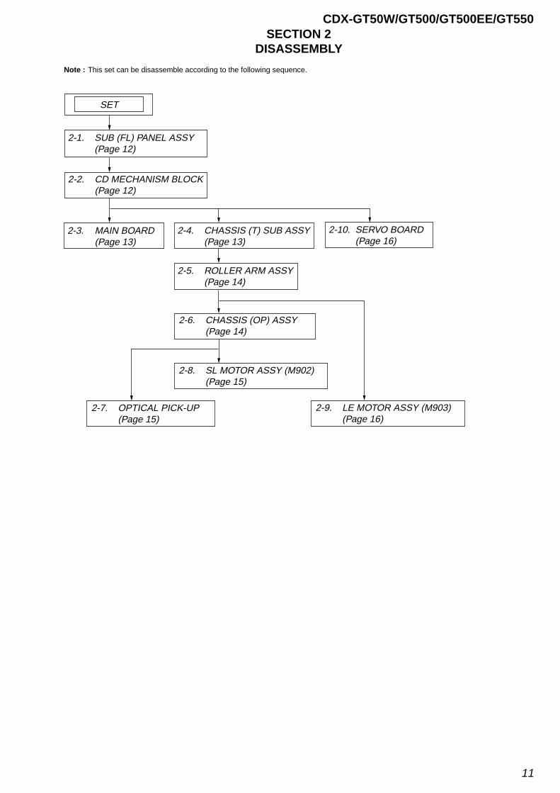
CDX-GT50W/GT500/GT500EE/GT550SECTION 2
DISASSEMBLY
Note : This set can be disassemble according to the following sequence.
2-1. SUB (FL) PANEL ASSY(Page 12)
2-2. CD MECHANISM BLOCK(Page 12)
SET
2-3. MAIN BOARD(Page 13)
2-4. CHASSIS (T) SUB ASSY(Page 13)
2-5. ROLLER ARM ASSY(Page 14)
2-6. CHASSIS (OP) ASSY(Page 14)
2-8. SL MOTOR ASSY (M902)(Page 15)
2-10. SERVO BOARD(Page 16)
2-7. OPTICAL PICK-UP(Page 15)
2-9. LE MOTOR ASSY (M903)(Page 16)
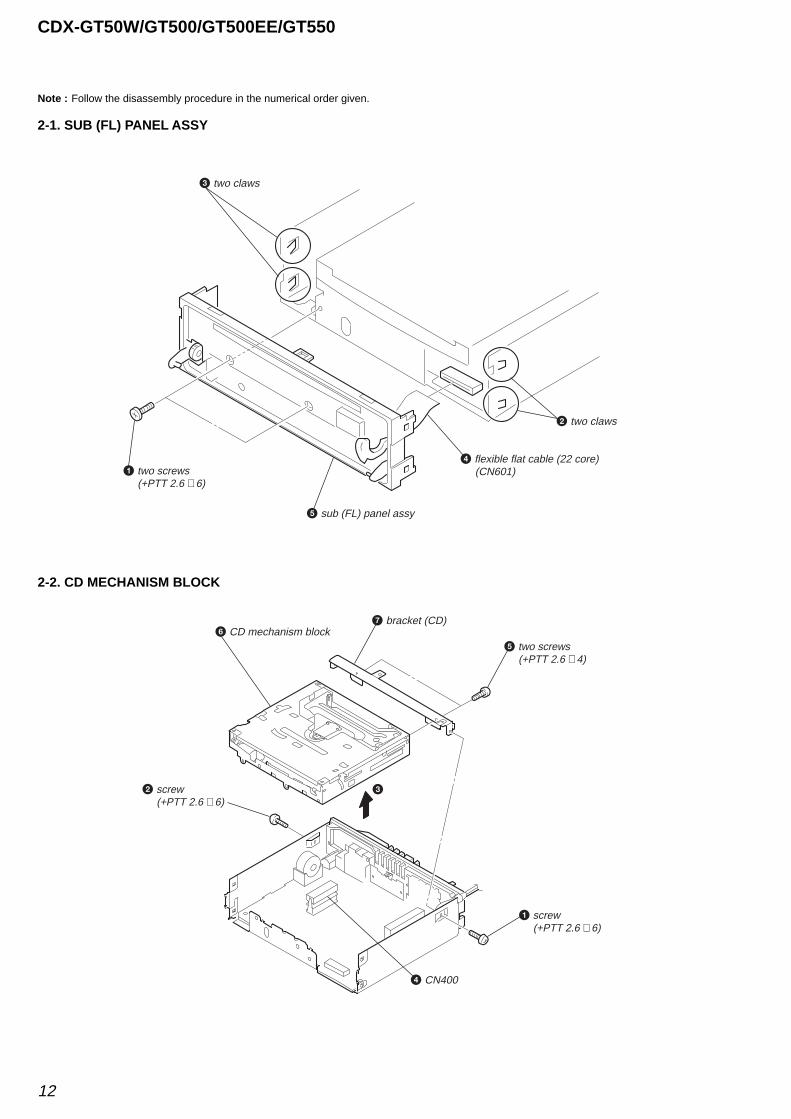
12
CDX-GT50W/GT500/GT500EE/GT550
2-2. CD MECHANISM BLOCK
Note : Follow the disassembly procedure in the numerical order given.
2-1. SUB (FL) PANEL ASSY
2 two claws
4 flexible flat cable (22 core) (CN601)
3 two claws
5 sub (FL) panel assy
1 two screws (+PTT 2.6 × 6)
7 bracket (CD)6 CD mechanism block
4 CN400
3
1 screw (+PTT 2.6 × 6)
2 screw (+PTT 2.6 × 6)
5 two screws (+PTT 2.6 × 4)
13
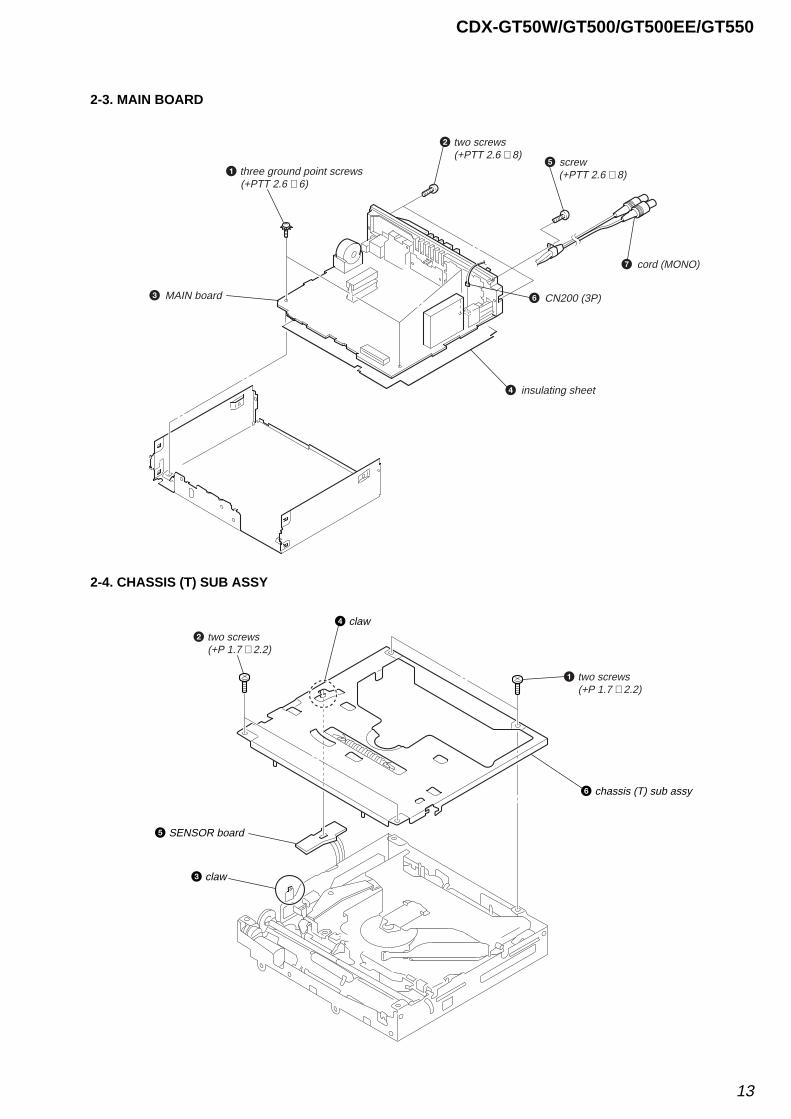
CDX-GT50W/GT500/GT500EE/GT550
2-4. CHASSIS (T) SUB ASSY
2-3. MAIN BOARD
1 three ground point screws (+PTT 2.6 × 6)
2 two screws (+PTT 2.6 × 8)
6 CN200 (3P)
5 screw (+PTT 2.6 × 8)
7 cord (MONO)
3 MAIN board
4 insulating sheet
5 SENSOR board
6 chassis (T) sub assy
4 claw
3 claw
1 two screws (+P 1.7 × 2.2)
2 two screws (+P 1.7 × 2.2)
14
CDX-GT50W/GT500/GT500EE/GT550
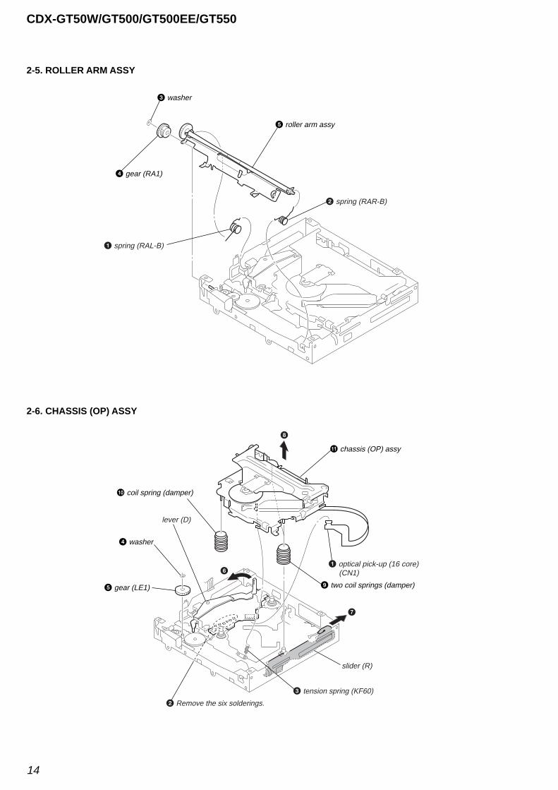
2-5. ROLLER ARM ASSY
2-6. CHASSIS (OP) ASSY
3 washer
4 gear (RA1)
5 roller arm assy
1 spring (RAL-B)
2 spring (RAR-B)
4 washer
0 coil spring (damper)
9 two coil springs (damper)
qa chassis (OP) assy
5 gear (LE1)
lever (D)
slider (R)
6
7
8
3 tension spring (KF60)
1 optical pick-up (16 core) (CN1)
2 Remove the six solderings.
15
CDX-GT50W/GT500/GT500EE/GT550
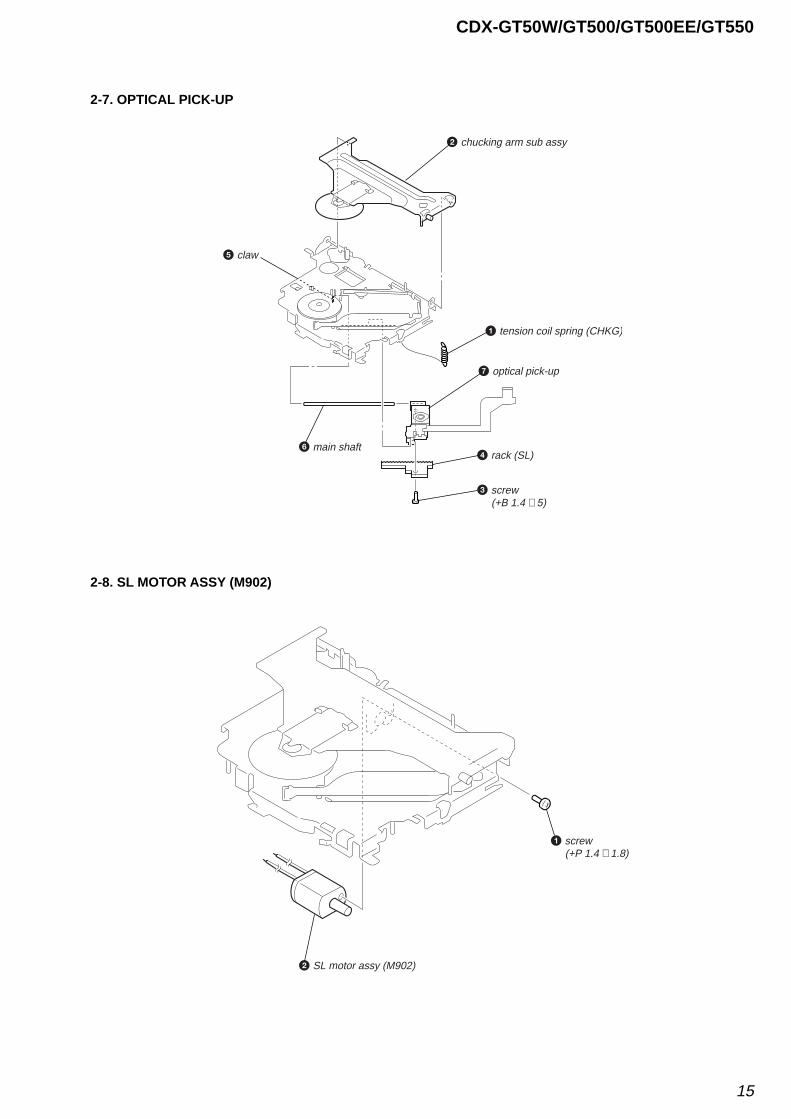
2-7. OPTICAL PICK-UP
2-8. SL MOTOR ASSY (M902)
1 tension coil spring (CHKG)
2 chucking arm sub assy
4 rack (SL)
5 claw
6 main shaft
7 optical pick-up
3 screw (+B 1.4 × 5)
1 screw (+P 1.4 × 1.8)
2 SL motor assy (M902)
16
CDX-GT50W/GT500/GT500EE/GT550
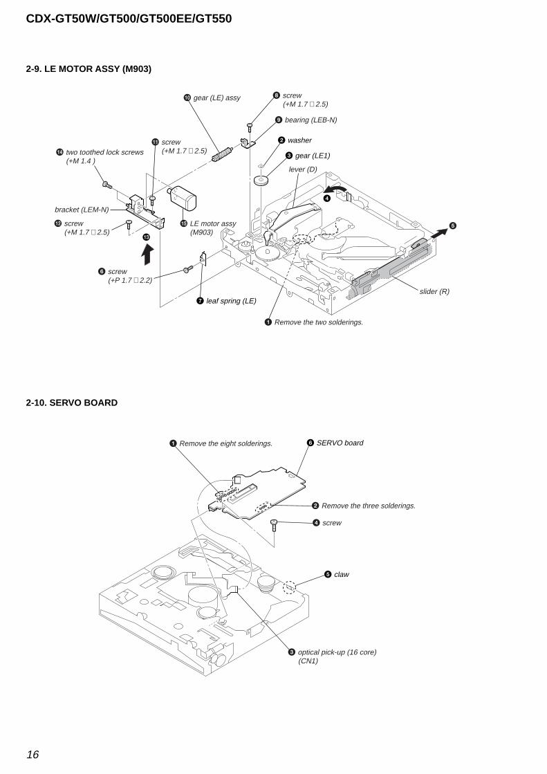
2-9. LE MOTOR ASSY (M903)
2-10. SERVO BOARD
2 washer
4
qd
3 gear (LE1)
7 leaf spring (LE)
5
lever (D)
bracket (LEM-N)
slider (R)
6 screw (+P 1.7 × 2.2)
8 screw (+M 1.7 × 2.5)
qa screw (+M 1.7 × 2.5)qf two toothed lock screws
(+M 1.4 )
qs screw (+M 1.7 × 2.5)
9 bearing (LEB-N)
0 gear (LE) assy
qg LE motor assy (M903)
1 Remove the two solderings.
5 claw
6 SERVO board
4 screw
1 Remove the eight solderings.
2 Remove the three solderings.
3 optical pick-up (16 core) (CN1)
17 17CDX-GT50W/GT500/GT500EE/GT550
CDX-GT50W/GT500/GT500EE/GT550
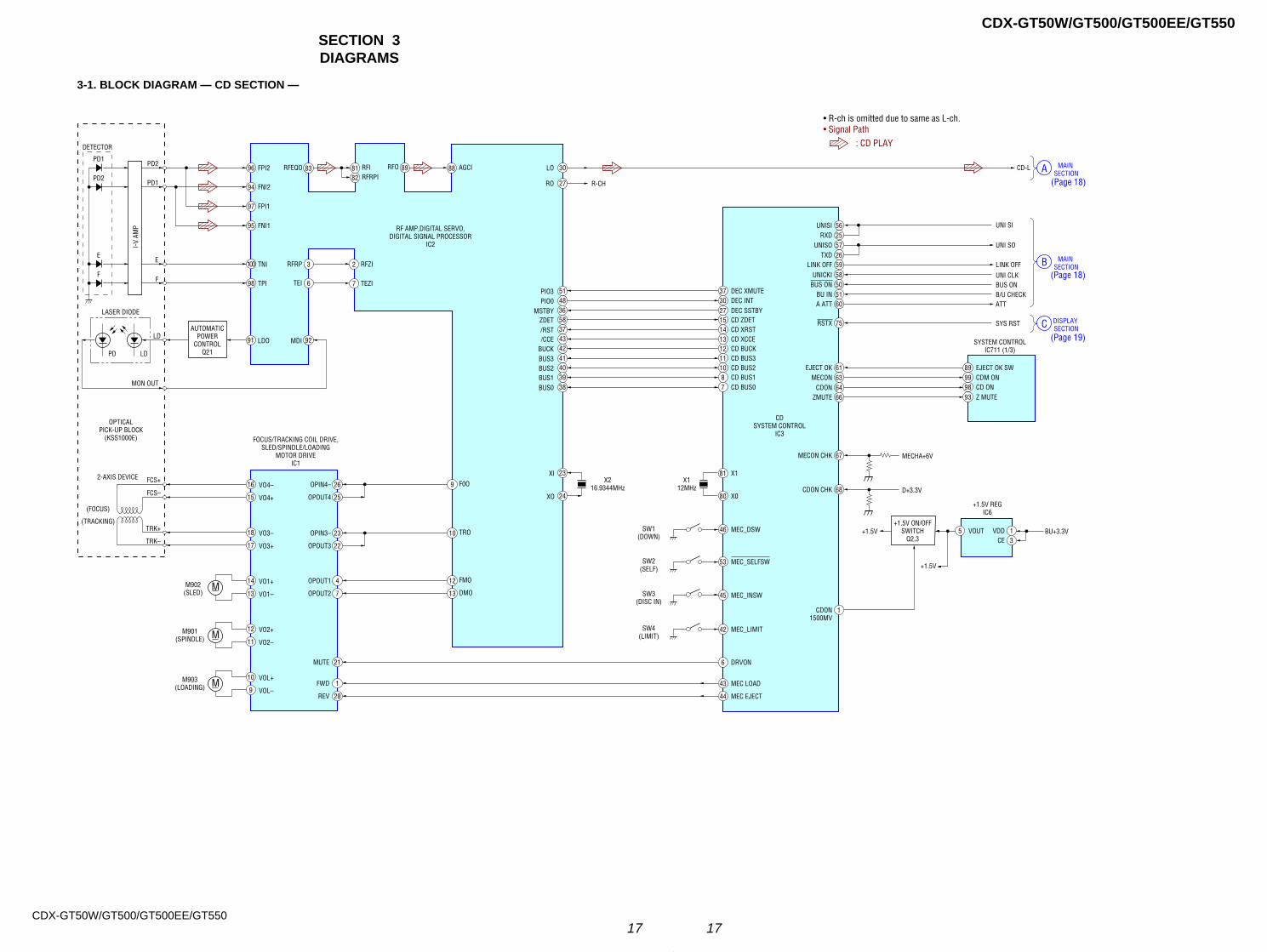
3-1. BLOCK DIAGRAM — CD SECTION —
SECTION 3DIAGRAMS
89RFO
RF AMP,DIGITAL SERVO,DIGITAL SIGNAL PROCESSOR
IC2
83RFEQO
3RFRP
6TEI
81 RFI82 RFRPI
2 RFZI
7 TEZI
9 F0O
PD1
PD2
E
F
I-V A
MP
PD LD
DETECTOR
88 AGCI
94
96
95
97
100
98
TNI
FPI1
FNI1
FPI2
FNI2
TPI
91 LDO 92MDI
(FOCUS)
(TRACKING)
2-AXIS DEVICE
OPTICALPICK-UP BLOCK
(KSS1000E)
• Signal Path: CD PLAY
LASER DIODE
M
M
M
18
17
VO3–
VO3+
14
13
VO1+
VO1–
12
11 VO2–
VO2+
10
9
VOL+
VOL–FWD
REV
1
28
OPIN4– 26
OPOUT4 25
10 TROOPIN3– 23
OPOUT3 22
12 FMOOPOUT1 4
13 DMOOPOUT2 7
MUTE 21
16
15
VO4–
VO4+
M903(LOADING)
M901(SPINDLE)
M902(SLED)
FOCUS/TRACKING COIL DRIVE,SLED/SPINDLE/LOADING
MOTOR DRIVEIC1
51PIO348PIO036MSTBY58ZDET37/RST43/CCE42BUCK41BUS3
CD-L MAIN SECTIONA30LO
27RO R-CH
27 DEC SSTBY15 CD ZDET14 CD XRST13 CD XCCE
53 MEC_SELFSW
45 MEC_INSW
42 MEC_LIMIT
12 CD BUCK11 CD BUS3
40BUS2 10 CD BUS239BUS1 8 CD BUS138BUS0 7 CD BUS0
81 X1
80 X0
MEC LOAD43
DRVON6
MEC EJECT44
CDSYSTEM CONTROL
IC3
+1.5V REGIC6
SYSTEM CONTROLIC711 (1/3)
37 DEC XMUTE30 DEC INT
SW2(SELF)
46 MEC_DSWSW1(DOWN)
SW3(DISC IN)
SW4(LIMIT)
56UNISI25RXD57UNISO
58UNICKI50BUS ON51BU IN
75RSTX
61EJECT OK
67MECON CHK
1CDON1500MV
63MECON64CDON66ZMUTE
60A ATT
26TXD
PD1
E
F
LD
MON OUT
FCS+
FCS–
TRK+
TRK–
PD2
AUTOMATICPOWER
CONTROLQ21
+1.5V ON/OFFSWITCH
Q2,3
• R-ch is omitted due to same as L-ch.
24
23X2
16.9344MHzX1
12MHz
XI
XO
DISPLAY SECTIONC
MAIN SECTIONB
EJECT OK SW
UNI SI
UNI SO
59LINK OFF LINK OFF
ATT
UNI CLKBUS ONB/U CHECK
SYS RST
89
CD ON
VOUT
98CDM ON99
Z MUTE
MECHA+6V
93
68CDON CHK
15 VDD3CE
D+3.3V
+1.5V
+1.5V
BU+3.3V
(Page 18)
(Page 18)
(Page 19)
1818CDX-GT50W/GT500/GT500EE/GT550
CDX-GT50W/GT500/GT500EE/GT550
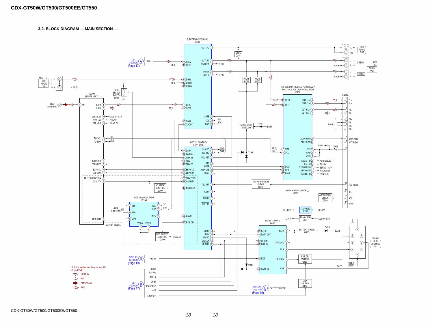
3-2. BLOCK DIAGRAM — MAIN SECTION —
(Page 17)
(Page 19)
(Page 17)(Page 19)
1 ANT 7 SE2L
ELECTRONIC VOLUMEIC401
J300(ANTENNA)
TU300(TUNER UNIT)
IC2-BUS CONTROLLED POWER AMP/MULTIPLE VOLTAGE REGULATOR
IC150
SYSTEM CONTROLIC711 (2/3)
CN100
8 SE2R
25 SAIN26 SAOUT
BATT
9 SE1L10 SE1R
11 DIFFL13 DIFFR
R-CH
43
10VCC+8.3V11VDD+5V15E2P VDD
13TU-SCL14TU-SDA
6S-METER7TU MUTE
16E2P SCL17E2P SDA
39 VSM17 AUX IN
45 SA CKO44 SA IN
AUDIO+8.3VTU+5VBU+3.3V
AEP,UK MODEL
12 TU ATT
25 EEP CKO24 EEP SIO
8MUTE CONDITION5QUALITY
RDS OUT
53 TU ATT IN38
13
QUALITY
NS MASK
DAVN
RDS ON
L-CHR-CH
AUXSELECTSWITCH
Q200
R-CH
1918
OUTLR1OUTRR1
16OUTLR2
R-CH
L
R
53
OUT FL+OUT FL–
97
OUT RL+OUT RL–
29
35
27AMP-REM
R-CH
ANT-REM
BATT
206
3037
AUDIO+BB.U+B
VP
VP1VP2
3133
SERVO3.3VMECHA6V
34PANEL+B
TU+5V
21MUTE
2 SDA
AUDIO+8.3VBU+5VSERVO+3.3VMECHA+6VPANEL+B
4 SCL
SDASCL
16 BEEP22 STB25 DIAG
AUDIO+8.3V
15
7
10
12
11
16
19
2
4
3
56
2223
SCLSDA
SCLSDA
SCLSDA
SCLSDA
33I2C CKO34I2C SIO
9VOL ATT
21ATT7BEEP26AMP STB8DIAG
73
30
UNISO
RESET
BUS ON
UNICLK
UNISI
B/U CHECK
LINK OFF
ATT
56
TEST IN
11 IN RL FL+FL–
RL+RL–
FR+FR–RR+RR–
AMP-REMANT-REM
ACC
TEST
12 IN FL
MUTEQ204
MUTE DRIVEQ250,251
NS MASKCONTROL
Q300
RDS DEMODULATORIC350
72
74
ACC IN
TEL ATT
ACCESSORYCHECKQ500
BUS ONSWITCH
Q453
LINK SWITCH
Q454
TU+5V REGQ301
BU+3.3V BU+5V+3.3V REGIC700
ILLUMINATION CHECKQ510
13TEL-MUTE
14ILL
D252
D250
F901
(L)
(R)
3
6
5
4
3
1
2
8
7
BATT BATT
BATT
6DATA I/O
4CLK
2RST
1BUS ON
BATTERY CHECKQ455
BUS INTERFACEIC450
D453
CNJ450
TH450
BUSCONTROL
IN
CD SECTION B
D457
1112
9
10
16
1 7
XTI SCLSCL
BU+3.3V
SDASDA
INTN
XTO
MPX
VDDA VDDD
TEL ATTENATIONCHECKQ520
RDS POWERCONTROL
Q350
915
X3508.664MHz
R-CH2017
OUTLFOUTRF
R-CH
L
RMUTEQ205
MUTEQ201
REAR
FRONT
54BU IN58UNISI59UNISO60UNISCK87BUSON
R-CH12 DIFFG
75ILLIN
RST13
BUS IN12CLK IN11
DATA OUT8B/U-C10
DATA IN9
DISPLAY SECTION D
CD-LCD SECTION A
BATTERY CHECKDISPLAY SECTION E
AUDIO OUT
J200(2/2)
R-CH
L
R
BUSAUDIO
IN
J200 (1/2)
SUBAUDIOOUT
• Signal Path• R-CH is omitted due to same as L-CH.
: CD PLAY
: FM
: AUX
: AM/MW/LW
19 19CDX-GT50W/GT500/GT500EE/GT550
CDX-GT50W/GT500/GT500EE/GT550
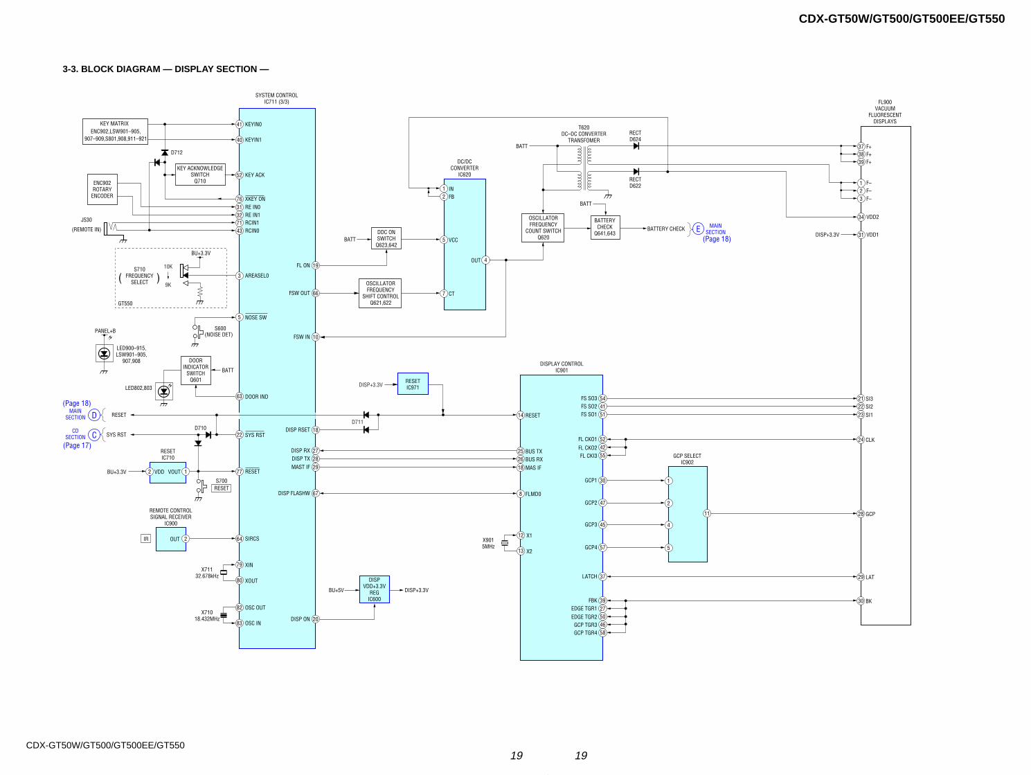
3-3. BLOCK DIAGRAM — DISPLAY SECTION —
(Page 17)
KEY ACKNOWLEDGESWITCH
Q710
X71132.678kHz
79
80
41
40
52
76
77
SYSTEM CONTROLIC711 (3/3) FL900
VACUUMFLUORESCENT
DISPLAYSKEYIN0
KEYIN1
71 RCIN1
31 RE IN0
43 RCIN0
KEY ACK
XKEY ON
3 AREASEL0
DOOR IND
BATT
22 SYS RST
RESET
63
2 1
XIN
XOUT
X71018.432MHz
82
83 OSC IN
OSC OUT
S700RESET
3837
39
D712
D710
S600
LED802,803
(NOISE DET)
LED900–915,LSW901–905,
907,908
F+F+F+
F–F–F–
21
3
BU+3.3V
SYS RST
KEY MATRIX
RESETIC710
IR
REMOTE CONTROLSIGNAL RECEIVER
IC900
OUT
ENC902,LSW901–905,907–909,S801,908,911–921
VDD VOUT
GCP SELECTIC902
1 IN2 FB
5 VCC
7 CT
RECTD624
T620DC–DC CONVERTER
TRANSFOMER
RECTD622
4OUT
BATT
BATTERY CHECK
BATT
BATT
64 SIRCS2
CDSECTION C
RESETMAIN
SECTION D
MAINSECTIONE
S710FREQUENCY
SELECT( )
BU+3.3V
J530
(REMOTE IN)
GT550
PANEL+B
10K
9K
5 NOSE SW
DDC ONSWITCH
Q623,642
BU+5V DISP+3.3V
DISPVDD+3.3V
REGIC600
DOORINDICATOR
SWITCHQ601
19FL ON
66FSW OUT
10FSW IN
20DISP ON
DC/DCCONVERTER
IC620
25 BUS TX26 BUS RX18 MAS IF
14 RESET
1
54FS SO341FS SO251FS SO1
52FL CKO1
FL CKO2FL CKI3
4255
30GCP1
247GCP2
445GCP3
28 GCP
24 CLK
23 SI122 SI221 SI3
11
557GCP4
8 FLMD0
DISPLAY CONTROLIC901
OSCILLATORFREQUENCY
SHIFT CONTROLQ621,622
RESETIC971
32 RE IN1
ENC902ROTARY
ENCODER
BATTERYCHECK
Q641,643
39FBK27EDGE TGR1
EDGE TGR2GCP TGR3GCP TGR4
504658
30 BK
29 LAT37LATCH
VDD1DISP+3.3V 31
VDD234
DISP+3.3V
D711
OSCILLATORFREQUENCY
COUNT SWITCHQ620
27DISP RX28DISP TX
29MAST IF
67DISP FLASHW
18DISP RSET
X9015MHz
12
13
X1
X2
(Page 18)
(Page 18)
2020CDX-GT50W/GT500/GT500EE/GT550
CDX-GT50W/GT500/GT500EE/GT550
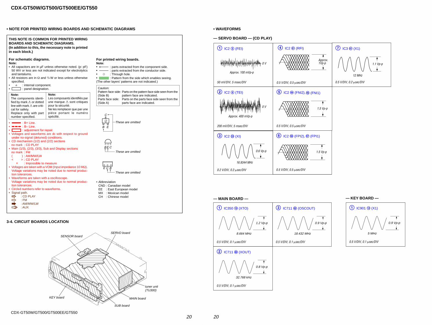
• NOTE FOR PRINTED WIRING BOARDS AND SCHEMATIC DIAGRAMS
THIS NOTE IS COMMON FOR PRINTED WIRINGBOARDS AND SCHEMATIC DIAGRAMS.(In addition to this, the necessary note is printedin each block.)
For schematic diagrams.Note:• All capacitors are in µF unless otherwise noted. (p: pF)
50 WV or less are not indicated except for electrolyticsand tantalums.
• All resistors are in Ω and 1/4 W or less unless otherwise
specified.• f : internal component.• C : panel designation.
For printed wiring boards.Note:• X : parts extracted from the component side.• Y : parts extracted from the conductor side.• a : Through hole.• : Pattern from the side which enables seeing.(The other layers' patterns are not indicated.)
• A : B+ Line.• B : B– Line.• H : adjustment for repair.• Voltages and waveforms are dc with respect to ground
under no-signal (detuned) conditions.• CD mechanism (1/2) and (2/2) sections no mark : CD PLAY• Main (1/3), (2/3), (3/3), Sub and Display sections no mark : FM
( ) : AM/MW/LW< > : CD PLAY
∗ : Impossible to measure• Voltages are taken with a VOM (Input impedance 10 MΩ).
Voltage variations may be noted due to normal produc-tion tolerances.
• Waveforms are taken with a oscilloscope.Voltage variations may be noted due to normal produc-tion tolerances.
• Circled numbers refer to waveforms.• Signal path.
J : CD PLAYF : FMf : AM/MW/LWL : AUX
Caution:Pattern face side: Parts on the pattern face side seen from the(Side B) pattern face are indicated.Parts face side: Parts on the parts face side seen from the(Side A) parts face are indicated.
• WAVEFORMS
— SERVO BOARD — (CD PLAY)
— MAIN BOARD —
1 IC2 5 (FEI)
Approx.1Vp-p0 V
0.6 Vp-p
16.9344 MHz
Approx. 100 mVp-p
50 mV/DIV, 5 msec/DIV
0.5 V/DIV, 0.5 µsec/DIV
2 IC2 6 (TEI)
200 mV/DIV, 5 msec/DIV
6 IC2 oh (FPI2),
0.5 V/DIV, 0.5 µsec/DIV
Approx. 400 mVp-p
3 IC2 wd (XI)
0.2 V/DIV, 0.2 µsec/DIV
7 IC3 ia (X1)
0.5 V/DIV, 0.2 µsec/DIV
1.1 Vp-p
12 MHz
4 IC2 ia (RFI)
0.5 V/DIV, 0.5 µsec/DIV
5 IC2 of (FNI2),og (FNI1)
1.5 Vp-p
oj (FPI1)
1.5 Vp-p
0 V
3-4. CIRCUIT BOARDS LOCATION 1.2 Vp-p
8.664 MHz
1 IC350 0 (XTO)
0.5 V/DIV, 0.1 µsec/DIV
0.8 Vp-p
32.768 kHz
2 IC711 i; (XOUT)
0.5 V/DIV, 0.1 µsec/DIV
0.9 Vp-p
18.432 MHz
3 IC711 is (OSCOUT)
0.5 V/DIV, 0.1 µsec/DIV
0.9 Vp-p
5 MHz
1 IC901 qs (X1)
0.5 V/DIV, 0.1 µsec/DIV
— KEY BOARD —
MAIN board
SUB board
SENSOR boardSERVO board
KEY board
tuner unit(TU300)
Q
C
These are omitted
EB
EThese are omitted
CB
CThese are omitted
BE
• AbbreviationCND : Canadian modelEE : East European modelMX : Mexican modelCH : Chinese model
Note:The components identi-fied by mark 0 or dottedline with mark 0 are criti-cal for safety.Replace only with partnumber specified.
Note:Les composants identifiés parune marque 0 sont critiquespour la sécurité.Ne les remplacer que par unepiéce portant le numérospécifié.
21 21CDX-GT50W/GT500/GT500EE/GT550
CDX-GT50W/GT500/GT500EE/GT550
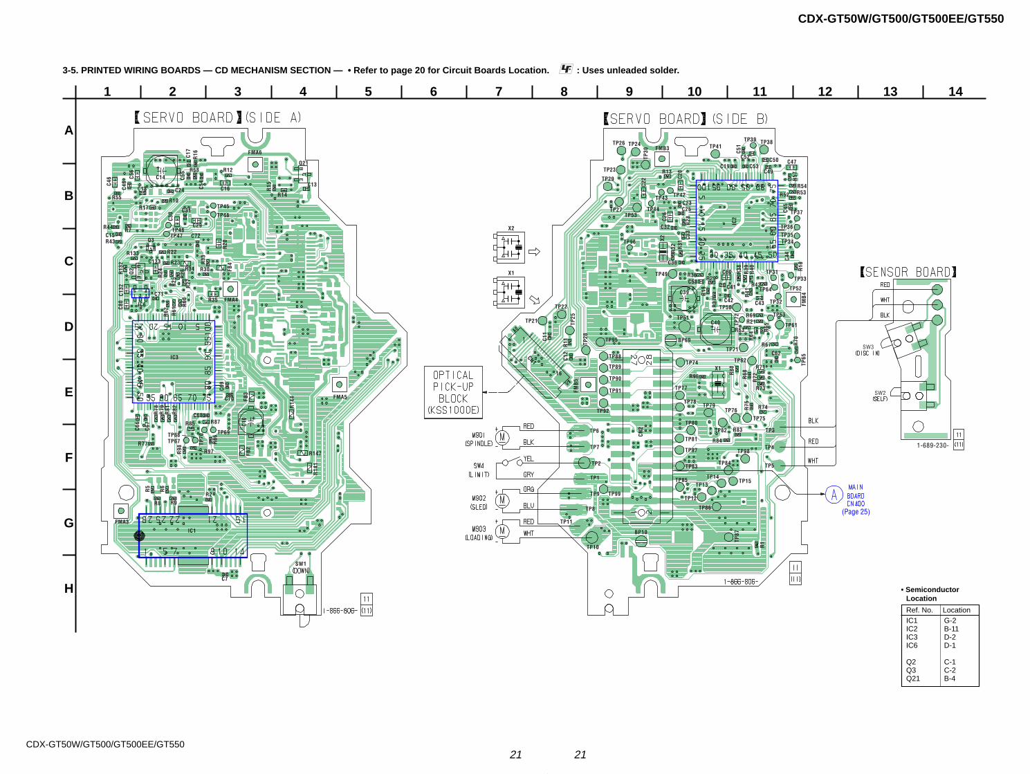
3-5. PRINTED WIRING BOARDS — CD MECHANISM SECTION — • Refer to page 20 for Circuit Boards Location. : Uses unleaded solder.
(Page 25)
Ref. No. Location
• SemiconductorLocation
IC1 G-2IC2 B-11IC3 D-2IC6 D-1
Q2 C-1Q3 C-2Q21 B-4
1
A
B
C
D
E
F
G
H
2 3 4 5 6 7 8 9 10 11 12 13 14
X1
X2
SW3
SW2
1-689-230-
FMA4
FMA6
FMA3
FMA5
TP67TP68
TP70
TP69
TP47TP48
TP45
TP46
IC6
R43
R35
C16
C70
C14
C29
C30
C68
C133
R10
C132
R16
R14
R15
C17
C72
R20
R5
R6
R26
R147
Q3
R8
R133
R13
2
Q21
SW1
C66
C67
C48
C10
R27
R17
R81
C46
R33
R44
R23
R22
R58
R9
R62 R61
IC3
R2
R60
C7
R87
R86
R85
R14
4
R82
R14
1
R79
R25
R78
R77R97R
98
R34
FB3
R55
FB2
C56
R24Q
2
IC1
C13
C80
C69
FB4
C18
R12
C71
C55
C54
R7
C31
C24
C15
R30
TP4
TP3
TP5
TP64
FMB3
FMB4
TP11
TP10
TP1
TP6
TP7
TP8
TP9
TP75TP76
TP77
TP78TP79
TP80
TP81
TP82
TP83
TP85
TP90
TP89
TP88
TP91
TP92
TP95
TP97
TP99
TP2
FMB5
IC2
TP86
TP87
TP84
TP98
TP14TP15
TP65
TP61
TP62
TP51
TP71
TP72
TP74
TP63
TP28
TP22
TP21
TP96
TP42TP43
TP44
TP29
TP34TP35
TP30
TP12
TP24
TP25
TP31
TP13
TP38TP41
TP49
TP50
TP53
TP32
TP33
TP36
TP37
TP39
TP52
BP60
TP23
TP26
TP27
BP10
R37
R36
R31
R32
R65
C40
C50
C23
R64
C60 R39
R63
X2
R54
C47
R53
R38
C43
R42
R52
C36
R28
CN2
R96
R41
C20
R84
R40
R83
R80
R75 R74
R69
R70
R73
R72
R71
R67
R68
C22 R
57
C26
R21
C39
C62
C58
R13
CN1
R11C1
1
C12
C53
C52
C49
C45
C44
C42
C41
C33
C32
C25
C19
R1
R18
R19
R29
C51
X116
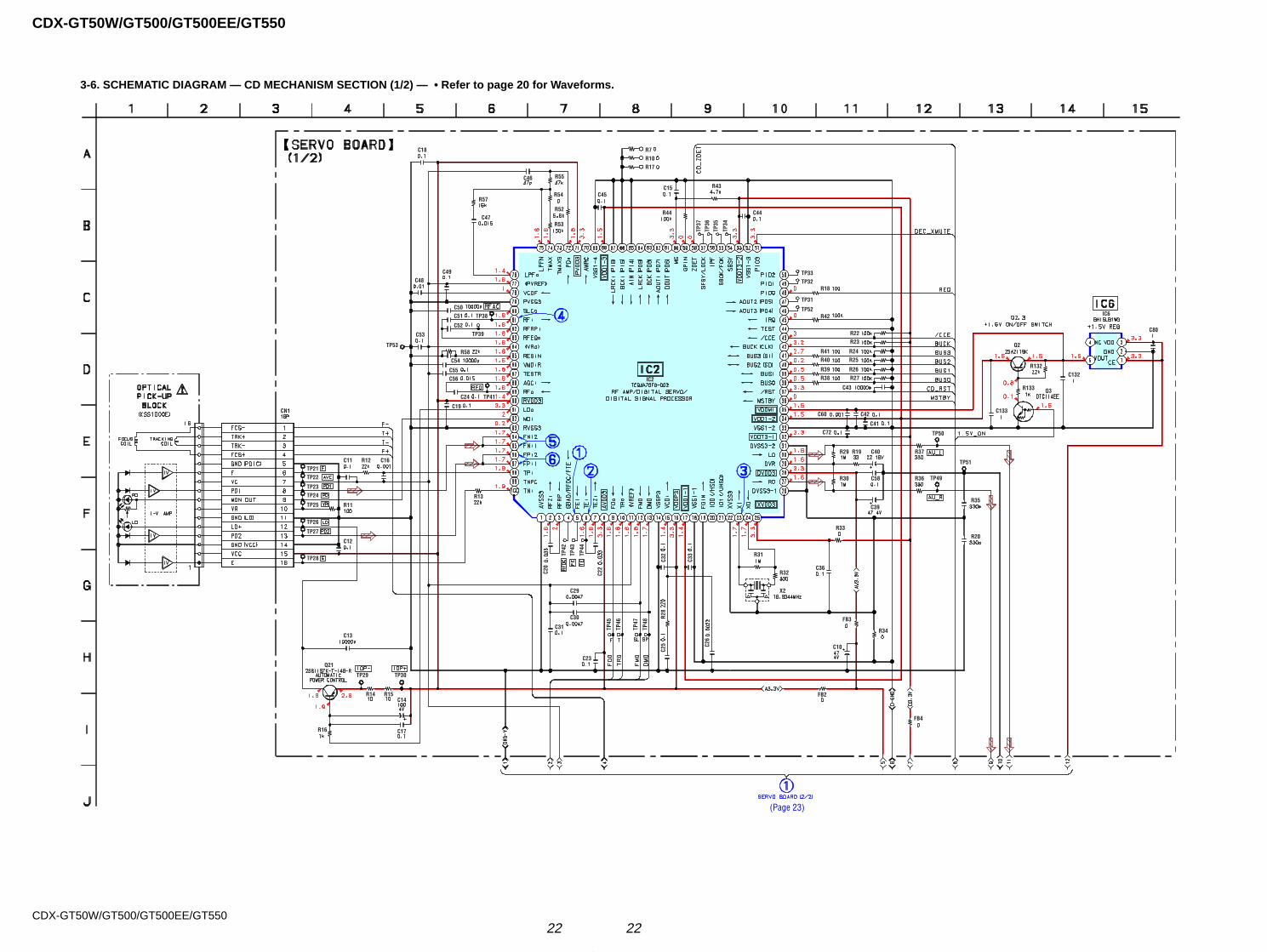
2222CDX-GT50W/GT500/GT500EE/GT550
CDX-GT50W/GT500/GT500EE/GT550
(Page 23)
3-6. SCHEMATIC DIAGRAM — CD MECHANISM SECTION (1/2) — • Refer to page 20 for Waveforms.
R14 R15
IC6
R132
R133
C10
TP21TP22
TP28
TP29 TP30
TP42
TP45
TP46
C39
R41R40
R39R38 R27
R25
R26
R24
R23R22
TP33TP32
TP37
TP36
R58
TP39
TP38
TP47
TP48
TP41
TP35
TP34
R42
TP50
TP49TP23TP24
TP25
TP26
TP27
TP52
TP31
R7R10R17
R18
C14
TP51
R57
R55
TP53
IC2
C12
C13
C17
C56
C54
C24
C55
C51C50
C53
C47
C49
C46
C22
C20
R28
FB2
FB3C31
C30
R36R30
C42
C41C72
C60
C43
C58
R29 R19
C132
C80
C133
C26
C25
C32
C33
R33
R31
R32
R34
C36TP
43
TP44
C29
C23
C40 R37
Q2
Q3
C15 R43
C44R44
C45
R53
R52
R54
C18
C48
C52
C19
R13
R12 C16
R16
R11
C11
FB4
CN1
X2
Q21
R35
R20
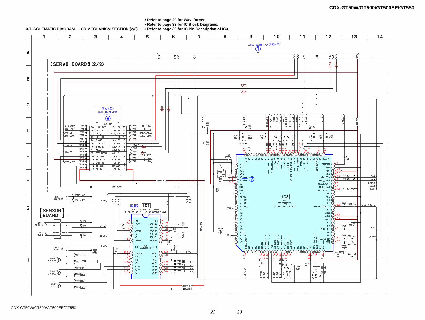
23 23CDX-GT50W/GT500/GT500EE/GT550
CDX-GT50W/GT500/GT500EE/GT550
• Refer to page 20 for Waveforms.• Refer to page 33 for IC Block Diagrams.
3-7. SCHEMATIC DIAGRAM — CD MECHANISM SECTION (2/2) — • Refer to page 36 for IC Pin Description of IC3.
(Page 27)
(Page 22)
IC B/D
R73
R72
R71
R83
TP67
TP68
TP69
TP72
TP63
TP64
TP65
R85
R77
R68
R67
R69
R60
R61
R62
R79
R80
R81
R82
R84
R70
TP15TP14
TP1
TP2
TP3
TP4
TP5
TP6
TP7
TP8
TP9
TP10
TP11
TP71
TP61
TP62
R64
R65
R21
TP12TP13
R141
R147
TP74TP75
TP76TP77
TP78TP79
TP80
TP81TP82TP83TP84
TP85TP86
TP87
TP88TP89
TP90TP91
TP92
TP97TP98
TP99
BP60
BP10
C69
C70
C68 C66
C62
C71
SW3
SW2
SW4
SW1
M901
M902
M903
C7IC1
R96
R74
R87
TP70
R75
R97
R98
R8
R5
R6
R2
R1
C67
CN2
R78
X1
R86
R144
IC3
R9
R63
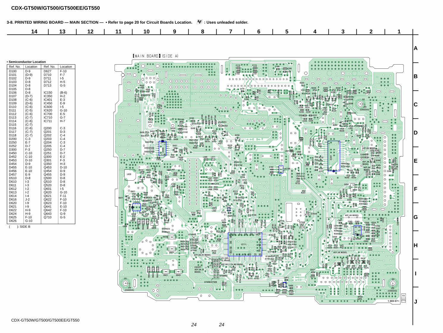
2424CDX-GT50W/GT500/GT500EE/GT550
CDX-GT50W/GT500/GT500EE/GT550
3-8. PRINTED WIRING BOARD — MAIN SECTION — • Refer to page 20 for Circuit Boards Location. : Uses unleaded solder.
Ref. No. Location
• Semiconductor Location
D100 D-9D101 (D-9)D102 D-9D103 D-8D104 D-8D105 D-8D106 D-8D107 (D-7)D108 (C-6)D109 (D-6)D110 (C-6)D111 (C-5)D112 (C-6)D113 (C-7)D114 (C-6)D115 (C-7)D116 (C-6)D117 (C-7)D118 (C-7)D200 C-3D250 E-7D252 D-7D300 F-3D450 C-10D452 C-10D453 D-10D454 D-9D455 E-10D456 E-10D457 E-9D510 D-8D610 I-3D611 I-3D612 I-2D613 I-2D614 I-4D616 J-2D620 I-9D621 I-9D622 H-9D624 H-9D625 F-10D626 G-10
D627 F-10D710 F-7D711 I-5D712 H-5D713 G-5
IC150 (B-6)IC350 H-2IC401 E-3IC450 E-9IC600 I-5IC620 G-10IC700 E-5IC710 G-7IC711 H-7
Q200 C-3Q201 D-3Q202 C-4Q203 C-4Q204 C-3Q205 C-4Q250 D-7Q251 D-7Q300 E-2Q301 F-3Q350 H-3Q453 D-10Q454 D-9Q455 D-9Q500 D-8Q510 D-8Q520 D-8Q601 I-5Q620 G-10Q621 F-11Q622 F-10Q623 F-10Q641 E-10Q642 F-10Q643 G-9Q710 G-5
Ref. No. Location
( ): SIDE B
1
A
B
C
D
E
F
G
H
I
J
234567891011121314
D624
R644
IC620
D622
R622
R623
R62
4
L902
L901
R620
R621R619
Q620
C903
C904
L410
R626
C102
D10
6C1
03
D10
4
C101
R103
D10
5
R521R520
Q520
R522D510
R510
R511
Q510
D100
D102
R500
R501R502
Q500
C154
C168
Q301
R31
1
C306
C309
D300
C308
C160
C163
C157
C702
C453
R461
R457
C153
C403
C151
L408
C407
L400
C402
L401
C161C162
R300R301
R302AEP,UK MODEL
AEP,UKMODEL
AEP,UK MODEL
AEP,UK MODEL
AEP,UKMODEL EXCEPT
AEP,UKMODEL
Q300
R303R304
R774C724
R305
R30
6
C361
R359
R353
C357
C358
C359
R35
5
C355
R352
C356 R354
Q350
C353
R351R350
C362C363R356
L350L351R358
R75
2
R307
R30
8
R309R310
Q453 Q454
R45
3
D450C450
D452 R455
D455
D456
Q455
R459
D454
D453
R45
8
R751
IC45
0
D457
R754
R71
2
R71
1
D710
IC710
IC700
C701
R725
C718
R72
9
R727
R730R731
R745
C710
R404
R717
L404
C406
L405
D250
R713
R407
R406
R532
R53
0R
531
R76
5
C727
D712
R733
R73
2
R72
2
R72
3R
720
R72
1R
724
R153
C173
C171R152
R728
GT500EE
GT500EE
GT50W/GT500/GT550
GT50W/GT500
US,CND,EE MODEL
AEP,UK,E,CH,MX MODEL
AEP,UK,EE MODEL
EXCEPTAEP,UK,EEMODEL
R72
6
R73
7
R201
C201
Q200
C719
C715
R718
C716
C717
R73
4
R735
R73
6
R742
R76
0
Q710
R76
8
R76
1R
762
C726 R764
R772
C725
R763R771
C721
R76
9
R77
0
R759R757
R755
R75
3
Q62
3
R632R633
D62
6
R631
R637
R636
Q62
2
R635
Q642
Q621R629
R628
R627
C624D625
R630
C625
Q64
1
C628
R20
3
D200R200
R20
4
R205 R206
R20
2
C217C220
C223
C229 R228
R226
R223
R221
R232
R230
R21
6
C159
R21
4
C158
C230
R229
R227 Q205
Q203
R22
4R
233
R21
7
C167 C1
66
R22
2
R231
R21
5
C170
C209C210
Q25
1
Q250
Q201D252
R251
C232
L201
R22
5
R220
R207
R208
R209
R210
C219
R616
R61
4
R615
R61
7
R758 R611
D612
D613
R61
8
R61
0
R613
R61
2
D61
0
D61
1
C612
Q60
1
L302
L300
C300
IC350
R63
9
R625
R77
5
R715 GT550
GT550
R716
R749R750
R746
R74
7
R78
0
R78
1R
782
C731
R766
R76
7
R40
3
R405
R450
R400
L406
L407
R748
R73
8
D711
R45
6
C627
D621
C728
C729
C601C6
00IC
600
C720Q643
R64
5
R648
R638
C642
C301C3
50
C310
Q202 Q204
C200
IC40
1
R245 R246
R255R256
R71
9
C352
R35
7
C360
C605
R743
D713
D103
L409
C713
C705
R634
G1 G2
C174C175
G3
(CHASSIS)
(CHASSIS) (CHASSIS)
D62
7R
652
R643 R65
3
D620
R65
1
R40
2
R401 L411
C246C256C257
R784R785
C644
IC711
L402
L403
C610
C611
C304
C730
D61
4
L200
L355
R605 R606R607
C236
C234
C233
C235
R21
8
C237
C238
C239
C240
FB301
R262
C231
D616
C733
R64
2
R65
4
R65
5
L620
R650
R100
C112
1-869-071- (11)
11
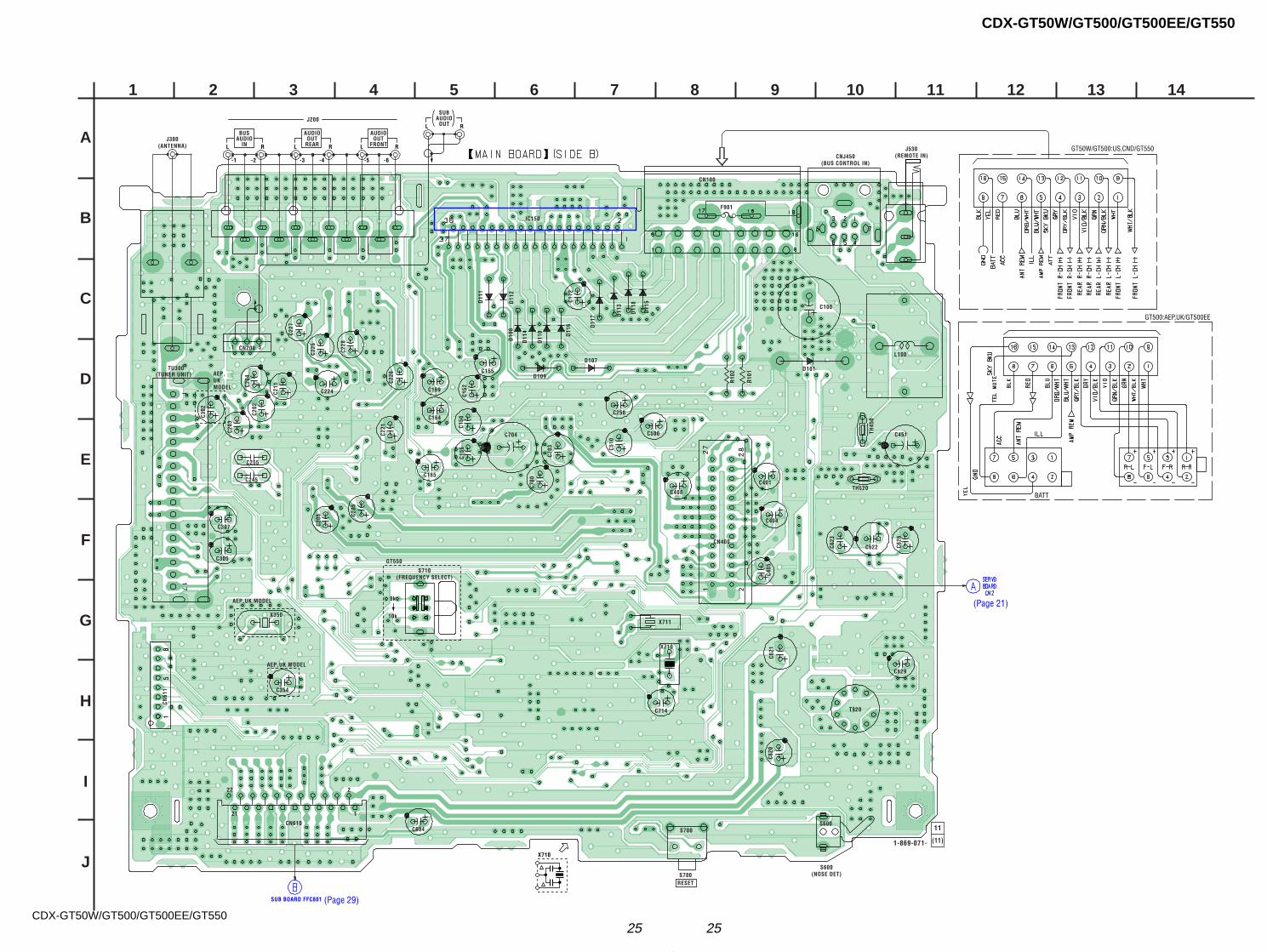
25 25CDX-GT50W/GT500/GT500EE/GT550
CDX-GT50W/GT500/GT500EE/GT550
(Page 29)
(Page 21)
1
A
B
C
D
E
F
G
H
I
J
2 3 4 5 6 7 8 9 10 11 12 13 14
X710
S700RESET
L RJ300
(ANTENNA)
BATT
GT50W/GT500:US,CND/GT550
GT500:AEP,UK/GT500EE
F901
BUSAUDIO
IN L R
AUDIOOUT
REAR L R
L RAUDIO
OUTFRONT
SUBAUDIO
OUT
C620
C621
CN100
C100
L100
D101
D11
8
D11
5
D11
7 D11
3
D11
6
D11
0
D11
4
D10
8
D107
D11
1
D109
D11
2
R10
2
C510
R10
1
C500
C169
C305
C307
C156
C164
C703
C152
C405
C150
C401
C302
C354
X350
GT550
AEP,UK MODEL
AEP,UK MODEL
TH45
0
C451
C700
C404
S710(FREQUENCY SELECT)
9k
10k
C165
C714
X710
X711
C623
C629
C202
C203
C204
C227
C225
C228
C226
C250
C206 C2
05
C224
CN610
21
22
1
2
SUB BOARD FFC801
C604 S700S600
S600(NOSE DET)
(TUNER UNIT)TU300
C626
C155
IC150
J200
CN2001
AEP,UKMODEL
3
C211
C245
C255
CNJ450(BUS CONTROL IN)
CN400C622
CN61
1
J530(REMOTE IN)
C408
C221
C172
T620
C704
TH620
-1 -2 -3 -4 -5 -6
1-869-071- (11)
11
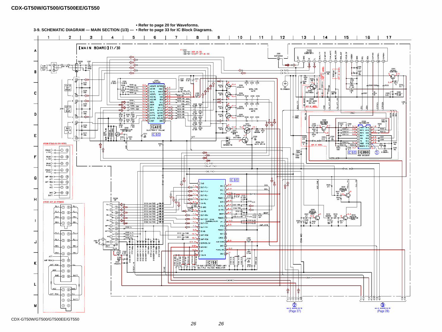
2626CDX-GT50W/GT500/GT500EE/GT550
CDX-GT50W/GT500/GT500EE/GT550
• Refer to page 20 for Waveforms.3-9. SCHEMATIC DIAGRAM — MAIN SECTION (1/3) — • Refer to page 33 for IC Block Diagrams.
IC B/D
IC B/D
IC B/DX350
R354
R353
R352 R355
R302R301
R300
C307R304
C302 C305
R305
R350
R351
R359
Q300
R311
C352
R500 C500R502
R521
R522
D510 R510
R511C510
C203R206
R202
R203
R20
0
C206
C205
R215
C211
L201
R201
R218
C202R205
R216R214
R217
R222
R221
R220
Q205R229
Q204R228
Q203R227
Q202R226
R225
R223
R231
R230
R233
R232
Q250 C250
R251D252
R255
R209
R208
R207
R210
D101
R153
R262
Q251
C217
C220
C223
C229
C230
C231C246 C256
C245
C255
C210
C209
C257
G3
C219
C201
C102
C158
C159
C174
C161
C175C162
C167
C170
C232
C240 C236
C239 C235
C238 C234
C173
C166
C904
L901
C301
C350
L355
C644
C362
C363
C356
C353
C361
C360
C359
C358C357
C355
C310
C309L300
C306
C308
L302
L100
C100
CN100
D118
D117
D115
D113
D116D110
D114D108
R103
R100
R101R102
C155C1
54
C153
C152C1
51
C150
C157
C156
D10
7C103
C101
D10
9C112
R520
C225
C226
C227
C228 R224
L200
C224
R246
R256
R245
C204
R204
C200
CN200
C237 C233
C304
R30
3
C354
R358
R357
R356
C169
C171
R152
C163
C164
C168
C160
C903
L902
C300
J300
D112
D111
J200
Q200
Q301
Q350
Q520
Q510
Q500
F901
D20
0
C221
Q201
D250
R308 R309 R310
FB30
1
R307D300
L351L350
R30
6
D10
0
D10
2
D10
3D
105
D10
4
D10
6
C172
TU300
IC350
IC150
IC401
R501C165
(Page 27) (Page 28)
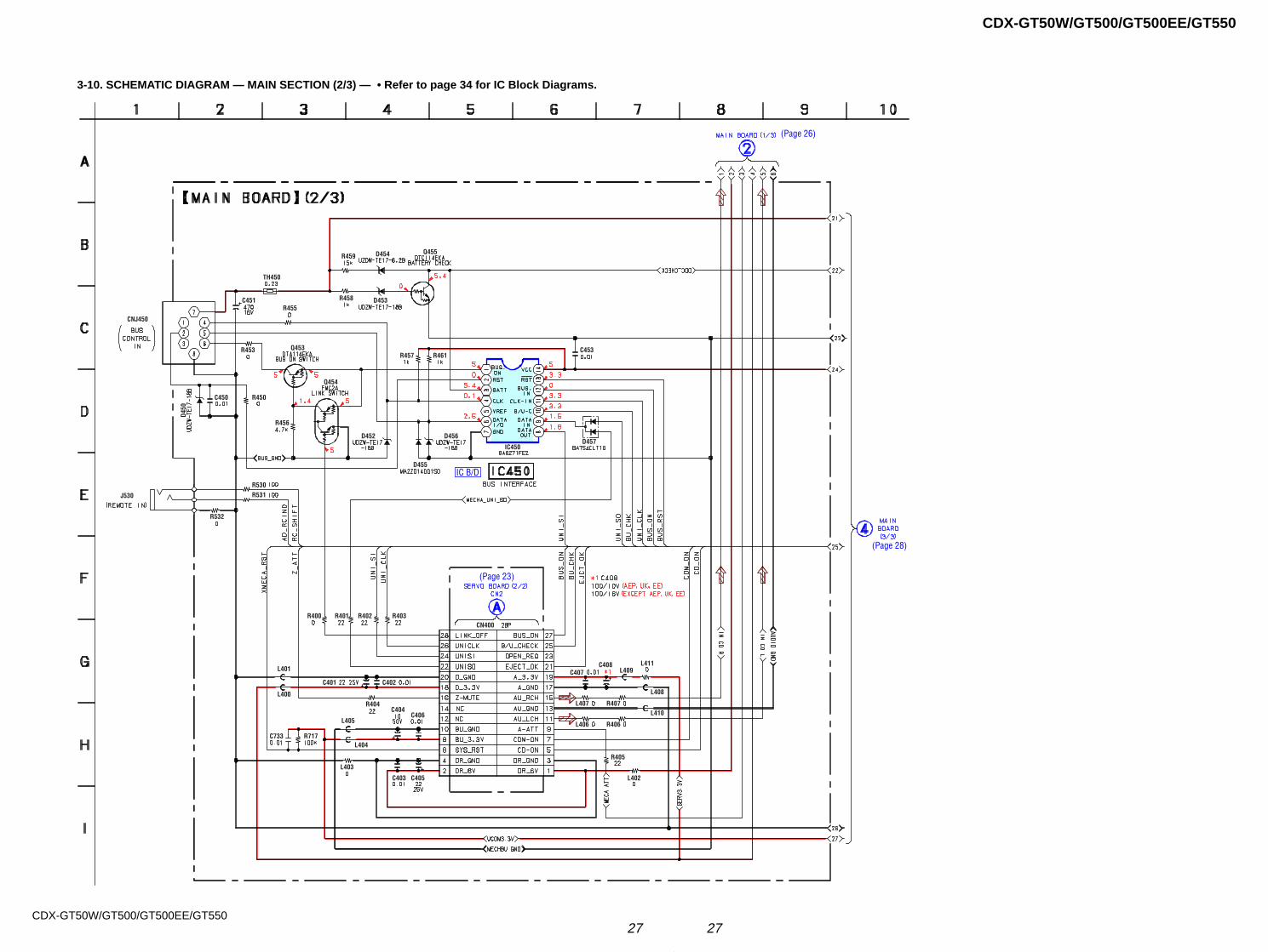
27 27CDX-GT50W/GT500/GT500EE/GT550
CDX-GT50W/GT500/GT500EE/GT550
(Page 28)
(Page 26)
3-10. SCHEMATIC DIAGRAM — MAIN SECTION (2/3) — • Refer to page 34 for IC Block Diagrams.
IC B/D
C405
C404
R406
R407
TH450
C451
R453R457
R455
D455
R461
R459
R458
R456
R401 R403R400
L407
L406
R450
R717C733
J530
C406
C403 L402
L411
C453
C450
R531R530
R532
CN400R402
C407
R405
C402C401
Q455
Q453
Q454
CNJ450
D454
D453
D45
0
D452 D456
IC450D457
C408L409
L408
L410
L404
L405
L401
L400
L403
R404
(Page 23)
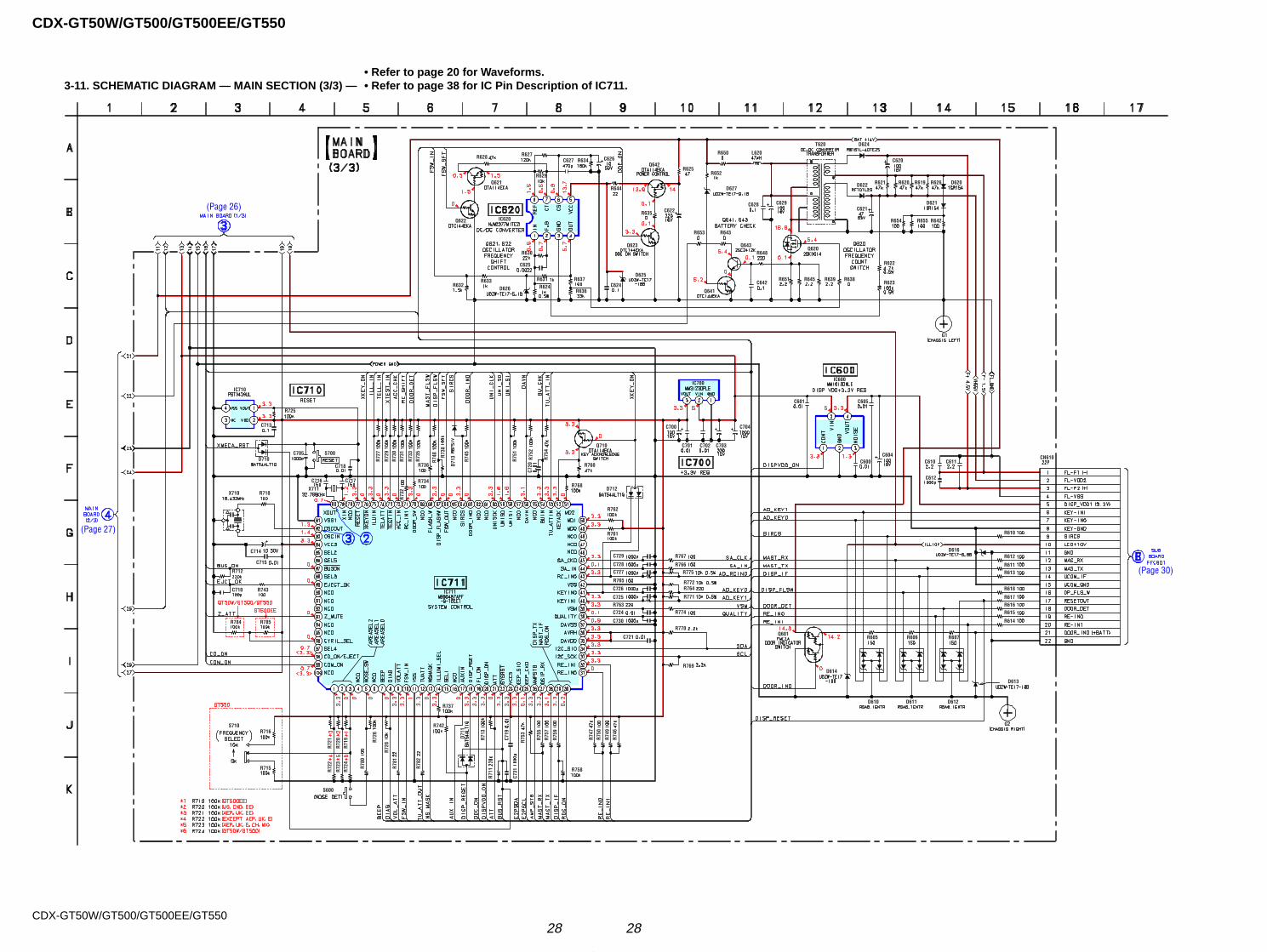
2828CDX-GT50W/GT500/GT500EE/GT550
CDX-GT50W/GT500/GT500EE/GT550
(Page 26)
(Page 27)
(Page 30)
• Refer to page 20 for Waveforms.3-11. SCHEMATIC DIAGRAM — MAIN SECTION (3/3) — • Refer to page 38 for IC Pin Description of IC711.
C703
X711
C704C700
R769
R774R763
R771
R75
4R
755
R75
7
R75
9
R75
3
R72
6
R72
8
R73
5
R742
R73
2
R75
1
R74
8
R761
R762
R768
R760
R725
R764
R71
3
R718
R75
2
R770
R772R765
R775R766
R767
R73
3
R73
0
R71
1
R72
9
R73
1
R72
7
R74
5
R74
6
R74
7
R73
8
R78
0
R78
1
R78
2
R784
S710
R613
R610
R611
R616
R612
R615
R617
R618
R614
D622
C621
C620
D621
D620
R636
R635
C629
R634
C622
C626
Q622
R628
R622
R623
R643
L620
R624R632R633 R631
R648
R629
R638
R644
R637
R652
Q641
D71
3
D610 D611 D612
R630
Q621
Q643
R785
G2
G1
C627
C625
R639R645R651C642
R654 R642R655
R650
C628
C710
C717C716
C718
C705
C713
C720
C731
C702C701
C605
R605 R606 R607
C611
C612
C610
C725
C721
C724
C730
C726
C727C728
C729
C601
C600C604
C714
C715
R743
IC710
R734
R736
R737
R75
0
R74
9
C719
R715
R716
C624
R627
R653
R621 R620 R619 R626
R712
Q642
Q623Q620
Q710S700
X710
S600
Q601
R758
CN610
IC620
D626
D625
D627
T620 D624
D616
D614
D613
D710
D712
IC711
D71
1
R72
2
R72
3R
724
R72
1
R72
0R
719
IC600IC700
R625
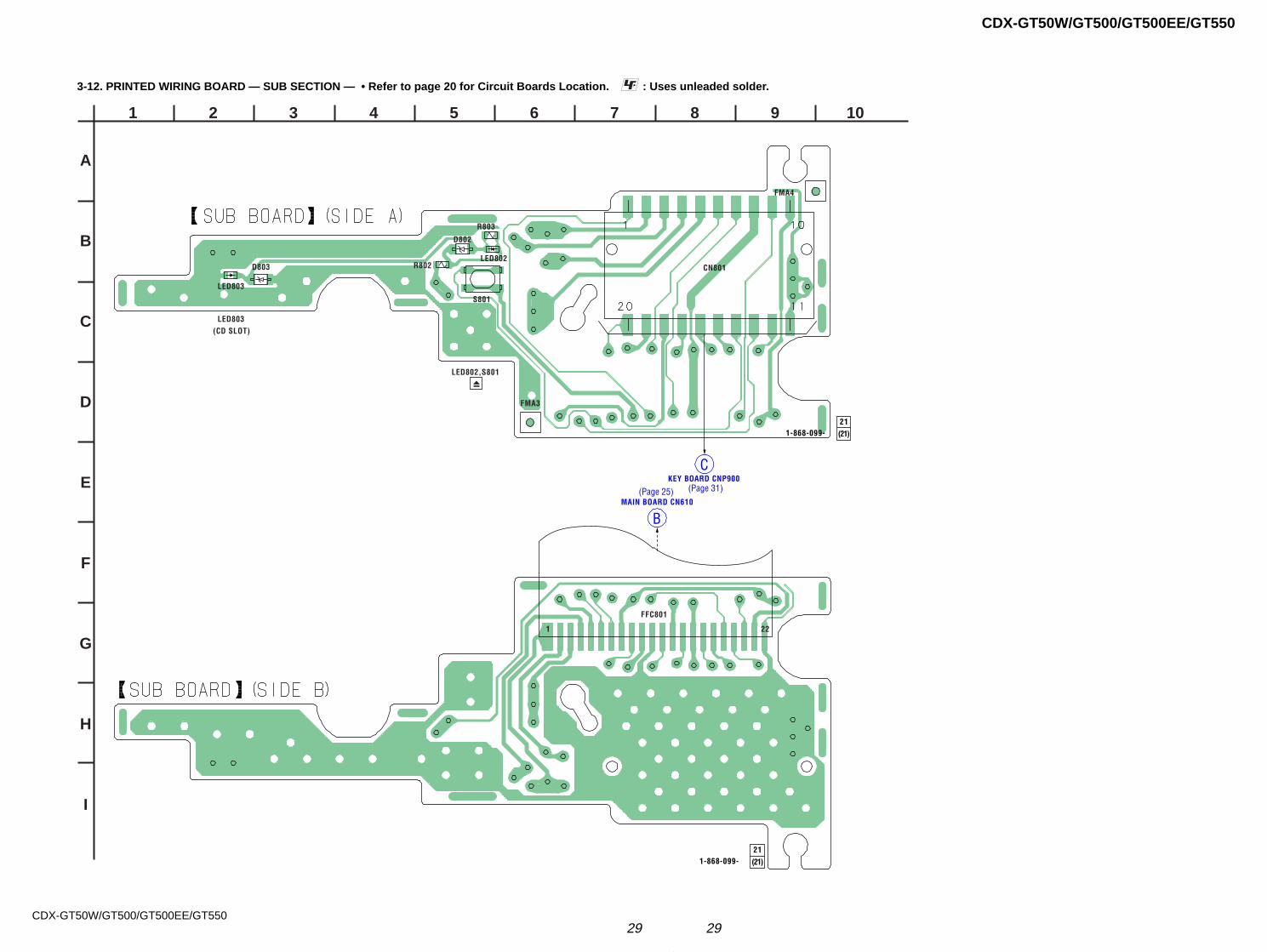
29 29CDX-GT50W/GT500/GT500EE/GT550
CDX-GT50W/GT500/GT500EE/GT550
(Page 25)
3-12. PRINTED WIRING BOARD — SUB SECTION — • Refer to page 20 for Circuit Boards Location. : Uses unleaded solder.
1
A
B
C
D
E
F
G
H
I
2 3 4 5 6 7 8 9 10
FMA3
1 22
FFC801
FMA4
LED802
LED802,S801
CN801
KEY BOARD CNP900
MAIN BOARD CN610
S801
D802
D803
LED803
LED803(CD SLOT)
Z
R803
R802
1-868-099- (21)21
1-868-099- (21)21
C
B
(Page 31)
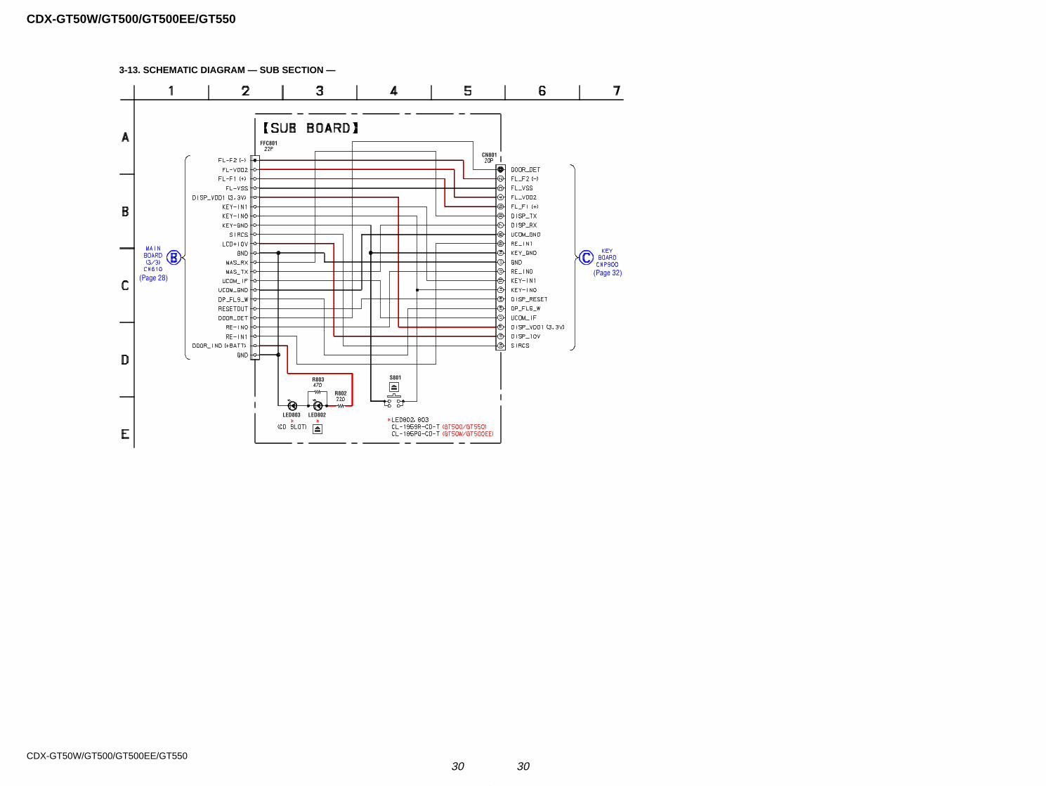
3030CDX-GT50W/GT500/GT500EE/GT550
CDX-GT50W/GT500/GT500EE/GT550
(Page 28)(Page 32)
3-13. SCHEMATIC DIAGRAM — SUB SECTION —
R803
FFC801
CN801
S801
R802
LED802LED803
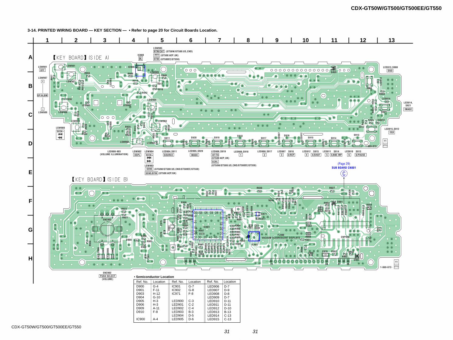
31 31CDX-GT50W/GT500/GT500EE/GT550
CDX-GT50W/GT500/GT500EE/GT550
3-14. PRINTED WIRING BOARD — KEY SECTION — • Refer to page 20 for Circuit Boards Location.
1
A
B
C
D
E
F
G
H
2 3 4 5 6 7 8 9 10 11 12 13
1-869-072- (11)
11
1-869-072- (11)
11
LSW901
LSW907+
–LSW909
SEEK–LSW908
OFF
GP/ALBM
MODE 21LED904,S911 LED905,S920 LED908,S917LED909,S918
SEEK+
SENS
LSW904DSPL SOURCE
LSW902LED900-903(VOLUME ILLUMINATION) 3
LED9073/REPS916
4LED912
6LED910
4/SHUFS915
5LED911
5/BBE MPS914
6/PAUSES913
DSOLED913,S908
AF/TALED906,S919
IC900
LSW905
BTM
ENC902PUSH SELECT
(VOLUME)
LED915,S912EQ3
LED914,S921
IMAGE
C
LSW903
BTM/CAT (GT50W/GT500:US,CND)
PTY (GT500:AEP,UK)
(GT500EE/GT550)
(GT50W/GT500:US,CND/GT500EE/GT550)
SENS/BTM (GT500:AEP/UK)
(GT50W/GT500:US,CND/GT500EE/GT550)SCRL
(GT500:AEP,UK)
IC900
LED904
LED
905
LED
906 LE
D90
7
LED
908
LED
909
LED
910
LED
911LE
D91
2
LED
913
LED914
LED915
LED
900
LED901 LED902
LED
903
S911 S920
S921
S912
S913S914S915
S916S917
S918S919
S908
R944
R93
7
R91
1R
912
R955
R936
R91
9
R92
0
R954
R935
R934R
913 R91
4
R91
5
R942R916
R917
R940
R918
R909
R93
3
R93
9 R92
5 R949
R92
4R
923
R950
LSW902
LSW901
LSW907
LSW908
LSW909 LSW903
LSW904
LSW905 D909
3
3 5
1 3 21 34 37 39
2 1
4
2 1
R983
R98
1
R98
0R
979
R97
7R
976
R97
5R
974
R97
3
R97
2R
970
R98
9
C984C904
C903
R921
R922
R93
8
R900
R901
R902
D900
C901
C976
C975
D90
5
D90
6
X901
R99
4R
985
C971
C985
R99
7
R996
R903 R90
8C9
72
IC901
R93
1
R93
2
C973R907
R984
R905
R990
C974
IC902
R94
8R
945
R946
R94
3 R94
7R
928
R92
9
R930
C977
R969R963
R995C981
IC971
R99
9
D91
0
R90
6
R99
3
C970
R968R967R965R966R964
R962
R991
CNP900
R904 D901
D90
4
R910
D903
R92
6
R927
C980
R951
R952
R953
R95
7
R95
9
R96
0R
961
R97
1R988
R958
R982
R99
8
C978 R992
R956
ENC902
FL900VACUUM FLUORESCENT DISPLAYS
SUB BOARD CN801(Page 29)
Ref. No. Location
• Semiconductor Location
D900 G-4D901 F-11D903 H-12D904 G-10D905 H-3D906 H-3D909 A-11D910 F-8
IC900 A-4
IC901 G-7IC902 G-8IC971 F-8
LED900 C-3LED901 C-2LED902 C-4LED903 B-3LED904 D-5LED905 D-6
Ref. No. Location Ref. No. Location
LED906 D-7LED907 D-9LED908 D-8LED909 D-7LED910 D-11LED911 D-11LED912 D-10LED913 B-13LED914 C-13LED915 C-13
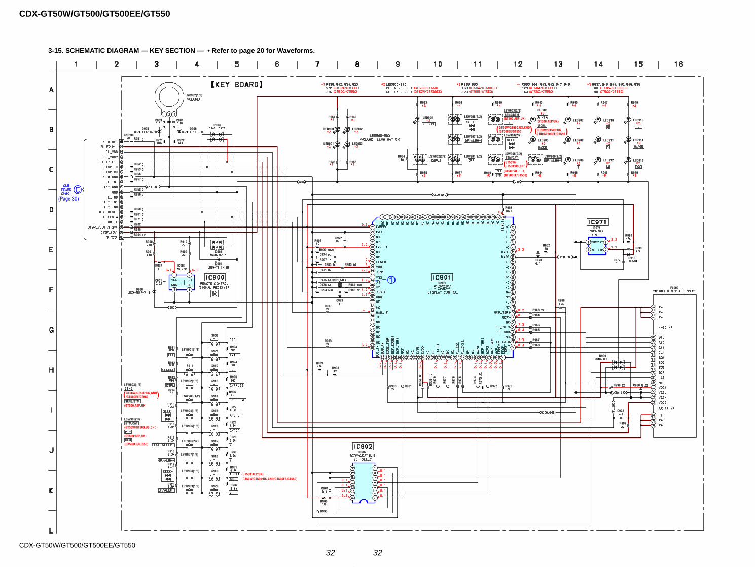
3232CDX-GT50W/GT500/GT500EE/GT550
CDX-GT50W/GT500/GT500EE/GT550
3-15. SCHEMATIC DIAGRAM — KEY SECTION — • Refer to page 20 for Waveforms.
(Page 30)
(GT500:AEP/UK)(GT50W/GT500:US,CND/GT500EE/GT550)
(GT500:AEP/UK)
GT50W/GT500:US,CND/GT500EE/GT550( )
GT50W/GT500:US,CND/GT500EE/GT550( )
(GT500:AEP,UK)
GT50W/GT500:US,CND(
( )
(GT500:AEP,UK)
)(GT500:AEP,UK)(GT500EE/GT550)
(GT500:AEP,UK)
(GT50W/GT500:US,CND)
(GT500EE/GT550)
SCRL
SCRL
SENS/BTM
LSW903(1/2)
GT50W/GT500:US,CND/GT500EE/GT550
SENS/BTM
LSW905(1/2)BTM/CAT
BTM
BTM/CAT
BTM
R984
R993
R994
R910R900
R901
R902
R909
R920 R932
R925
R912
R913
R926
R927
R914
R915
R928
R929
R916
R917
R930
R924
R923
R918
R911
R919R931
X901
R985
IC902
R98
0
R905
R996
R990
R997
R951
R952
R953
R957
R959
R962
R922R921
R969
D910
R991
R999
R903
R908
R963
R970
R97
3
R906
R958
C901
LSW901(1/2)
S911
LSW902(1/2)
LSW903(1/2)
LSW904(1/2)
LSW905(1/2)
ENC902(2/2)
LSW907(1/2)
LSW908(1/2)
LSW909(1/2) S920
S919
S918
S917
S916
S915
S914
S913
S912
S921
S908
CNP900
ENC902(1/2)
C903 C904
C981
C973
C971
C985
C974
C972
R954 R942
LED900 LED902
LED901 LED903
R938 R955
C984
C970 C977
R946 R948 R950
R992
R998 C980
IC900
R989
R907
C975C976
IC971
R983
R904
R971R961
R960
LED904 LSW908(2/2)
LSW907(2/2)
LSW901(2/2)LSW902(2/2)
LSW903(2/2)
LSW904(2/2)
LSW905(2/2)
R940 R944R937R935
LSW909(2/2)
LED905
LED906
LED907
LED908
LED909 LED912
LED911
LED913
LED914
LED915LED910
R949R947R945R943R939R936R933
D905D903
R956
R982R988
D900
D901
D904
IC901
R995
R97
9
R97
7
R97
6
R97
5
R97
4
R972
R968R967
R965R966
R964
R981
D909
C978
FL900
D906
R934
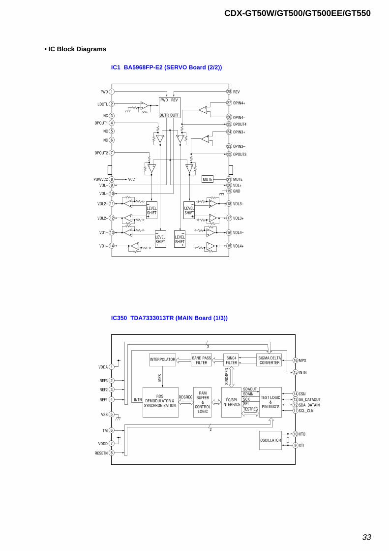
33
CDX-GT50W/GT500/GT500EE/GT550
• IC Block Diagrams
IC1 BA5968FP-E2 (SERVO Board (2/2))
1
2
11
13
14
12
LEVELSHIFT
LEVELSHIFT
LEVELSHIFT
LEVELSHIFT
MUTE
FWD
FWD
LDCTL
NC
OPOUT1
NC
NC
OPOUT2
POWVCC VCCVOL–
VOL+
VOL2–
VOL2+
VO1–
VO1+
REV
OPIN4+
OPIN4–
OPOUT4
OPIN3+
OPIN3–
OPOUT3
MUTEVOL+GND
VOL3–
VOL3+
VOL4–
VOL4+
REV
OUTR OUTF
10
98
7
6
5
28
27
26
25
24
23
22
212019
18
17
16
15
4
3
IC350 TDA7333013TR (MAIN Board (1/3))
VDDA
INTERPOLATOR
RAMBUFFER
&CONTROL
LOGIC
TEST LOGIC&
PIN MUX'S
I2C/SPI
INTERFACE
BAND PASSFILTER
SIGMA DELTACONVERTER
SINC4FILTER
REF3
REF2
REF1
VSS
VDDD
RESETN
TM
1
MPX16
CSNSDAOUT
RDSREG
3
INTN
MPX
SINC
4REG
SDAINSCKSPITESTREG
14
2
3
4
5
6
7
8
INTN15
SA_DATAOUT13SDA_DATAIN12SCL_CLK11
OSCILLATOR
XTO10
XTI9
RDSDEMODULATOR &
SYNCHRONIZATION
2
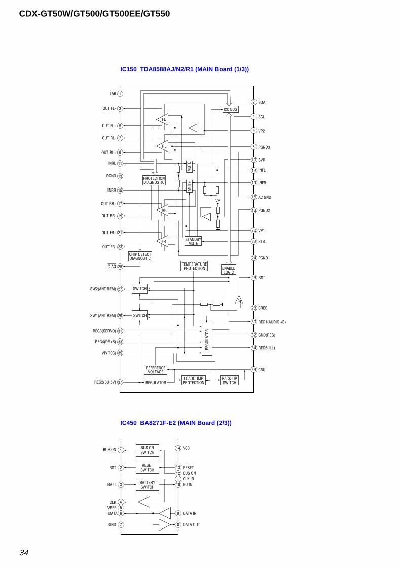
34
CDX-GT50W/GT500/GT500EE/GT550
IC150 TDA8588AJ/N2/R1 (MAIN Board (1/3))
MUT
EM
UTE
ENABLELOGIC
STANDBYMUTE
CHIP DETECTDIAGNOSTIC
PROTECTIONDIAGNOSTIC
SWITCH
REGU
LATO
R
SWITCH
REFERENCEVOLTAGE
LOADDUMPPROTECTION
TEMPERATUREPROTECTION
BACK-UPSWITCHREGULATOR
1
3
5
7
9
11
13
15
17
19
21
23
25
27
29
31
33
35
37
2
4
6
8
10
12
14
16
18
20
22
24
26
28
30
32
34
36
TAB
OUT FL-
OUT FL+
OUT RL-
OUT RL+
INRL
SGND
INRR
OUT RR+
OUT RR-
OUT FR+
OUT FR-
DIAG
SW2(ANT REM)
SW1(ANT REM)
REG3(SERVO)
REG4(DR+B)
VP(REG)
REG2(BU 5V)
SDA
SCL
VP2
PGND3
SVR
INFL
INFR
AC GND
PGND2
VP1
STB
PGND1
RST
CRES
REG1(AUDIO +B)
GND(REG)
REG5(ILL)
CBU
FL
RL
RR
VP
FR
I2C BUS
IC450 BA8271F-E2 (MAIN Board (2/3))
1
2
3
456
7 8
9
10
14
131211
BUS ONSWITCH
RESETSWITCH
BATTERYSWITCH
BUS ON
RST
BATT
CLKVREF
GND
VCC
RESETBUS ONCLK INBU IN
DATA IN
DATA OUT
DATA
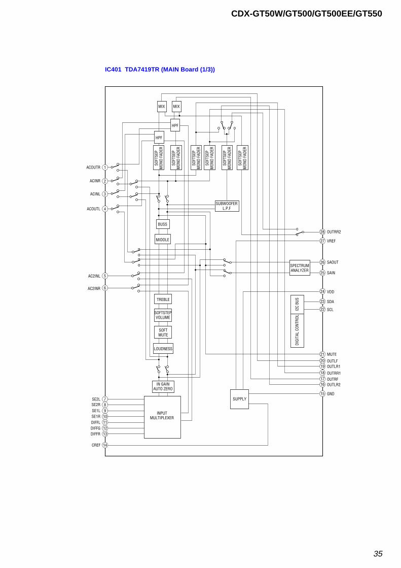
35
CDX-GT50W/GT500/GT500EE/GT550
IC401 TDA7419TR (MAIN Board (1/3))
2
3
1
4
5
6
7 SUPPLY
I2C
BUS
DIGI
TAL
CONT
ROL
INPUTMULTIPLEXER
15
181716
1920
21
22
23
24
27
25
26
28
89
10111213
14
SOFT
SEP
MON
O FA
DER
SOFT
SEP
MON
O FA
DER
SOFT
SEP
MON
O FA
DER
SUBWOOFERL.P.F
MIX MIX
HPF
BUSS
MIDDLE
SPECTRUMANALYZER
TREBLE
SOFTSTEPVOLUME
IN GAINAUTO ZERO
SOFTMUTE
LOUDNESS
HPF
SOFT
SEP
MON
O FA
DER
SOFT
SEP
MON
O FA
DER
SOFT
SEP
MON
O FA
DER
ACOUTR
ACINR
ACINL
ACOUTL
AC2INL
AC2INR
SE2LSE2RSE1LSE1RDIFFLDIFFGDIFFR
CREF
GND
OUTLR2OUTRFOUTRR1
OUTLR1OUTLF
MUTE
SCL
SDA
VDD
SAIN
SAOUT
VREF
OUTRR2
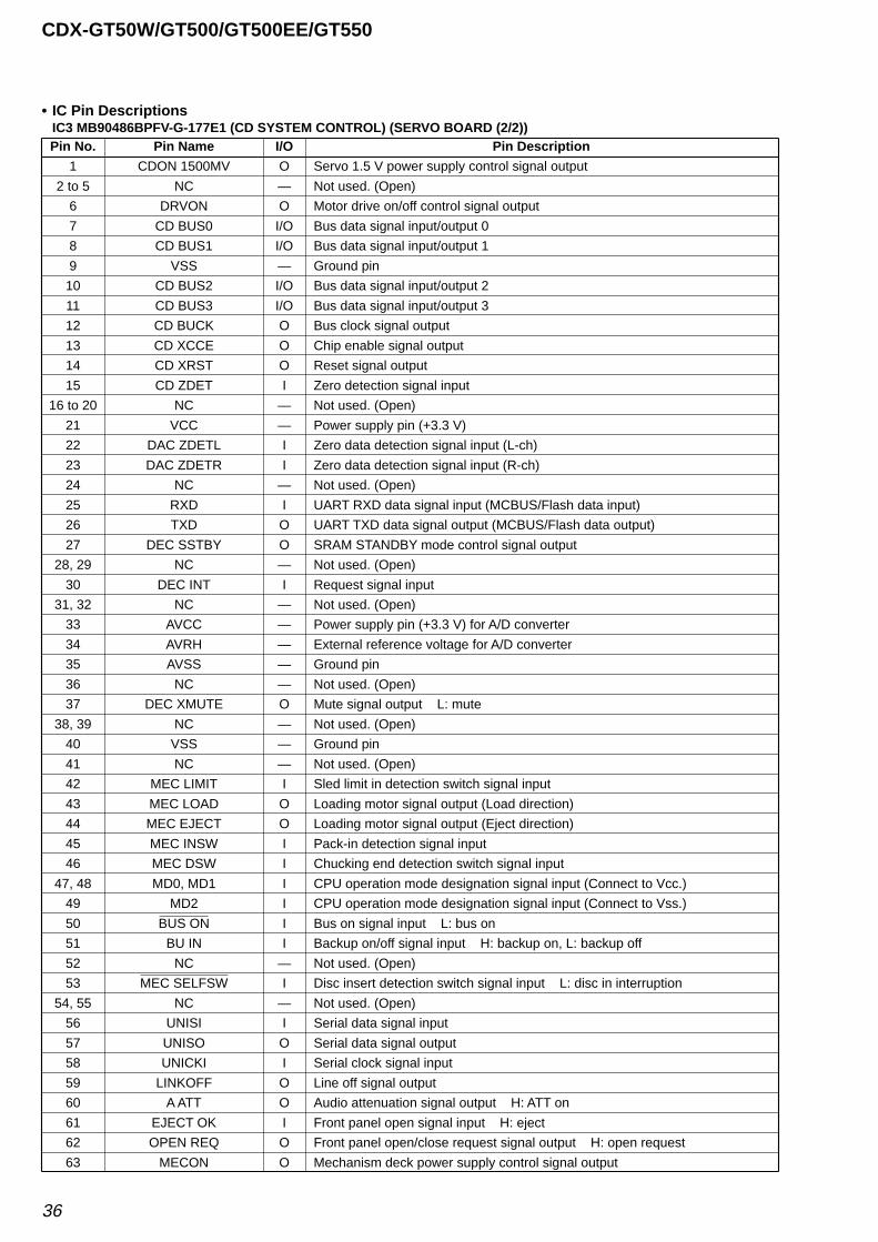
36
CDX-GT50W/GT500/GT500EE/GT550
• IC Pin DescriptionsIC3 MB90486BPFV-G-177E1 (CD SYSTEM CONTROL) (SERVO BOARD (2/2))Pin No. Pin Name I/O Pin Description
1 CDON 1500MV O Servo 1.5 V power supply control signal output
2 to 5 NC — Not used. (Open)
6 DRVON O Motor drive on/off control signal output
7 CD BUS0 I/O Bus data signal input/output 0
8 CD BUS1 I/O Bus data signal input/output 1
9 VSS — Ground pin
10 CD BUS2 I/O Bus data signal input/output 2
11 CD BUS3 I/O Bus data signal input/output 3
12 CD BUCK O Bus clock signal output
13 CD XCCE O Chip enable signal output
14 CD XRST O Reset signal output
15 CD ZDET I Zero detection signal input
16 to 20 NC — Not used. (Open)
21 VCC — Power supply pin (+3.3 V)
22 DAC ZDETL I Zero data detection signal input (L-ch)
23 DAC ZDETR I Zero data detection signal input (R-ch)
24 NC — Not used. (Open)
25 RXD I UART RXD data signal input (MCBUS/Flash data input)
26 TXD O UART TXD data signal output (MCBUS/Flash data output)
27 DEC SSTBY O SRAM STANDBY mode control signal output
28, 29 NC — Not used. (Open)
30 DEC INT I Request signal input
31, 32 NC — Not used. (Open)
33 AVCC — Power supply pin (+3.3 V) for A/D converter
34 AVRH — External reference voltage for A/D converter
35 AVSS — Ground pin
36 NC — Not used. (Open)
37 DEC XMUTE O Mute signal output L: mute
38, 39 NC — Not used. (Open)
40 VSS — Ground pin
41 NC — Not used. (Open)
42 MEC LIMIT I Sled limit in detection switch signal input
43 MEC LOAD O Loading motor signal output (Load direction)
44 MEC EJECT O Loading motor signal output (Eject direction)
45 MEC INSW I Pack-in detection signal input
46 MEC DSW I Chucking end detection switch signal input
47, 48 MD0, MD1 I CPU operation mode designation signal input (Connect to Vcc.)
49 MD2 I CPU operation mode designation signal input (Connect to Vss.)
50 BUS ON I Bus on signal input L: bus on
51 BU IN I Backup on/off signal input H: backup on, L: backup off
52 NC — Not used. (Open)
53 MEC SELFSW I Disc insert detection switch signal input L: disc in interruption
54, 55 NC — Not used. (Open)
56 UNISI I Serial data signal input
57 UNISO O Serial data signal output
58 UNICKI I Serial clock signal input
59 LINKOFF O Line off signal output
60 A ATT O Audio attenuation signal output H: ATT on
61 EJECT OK I Front panel open signal input H: eject
62 OPEN REQ O Front panel open/close request signal output H: open request
63 MECON O Mechanism deck power supply control signal output
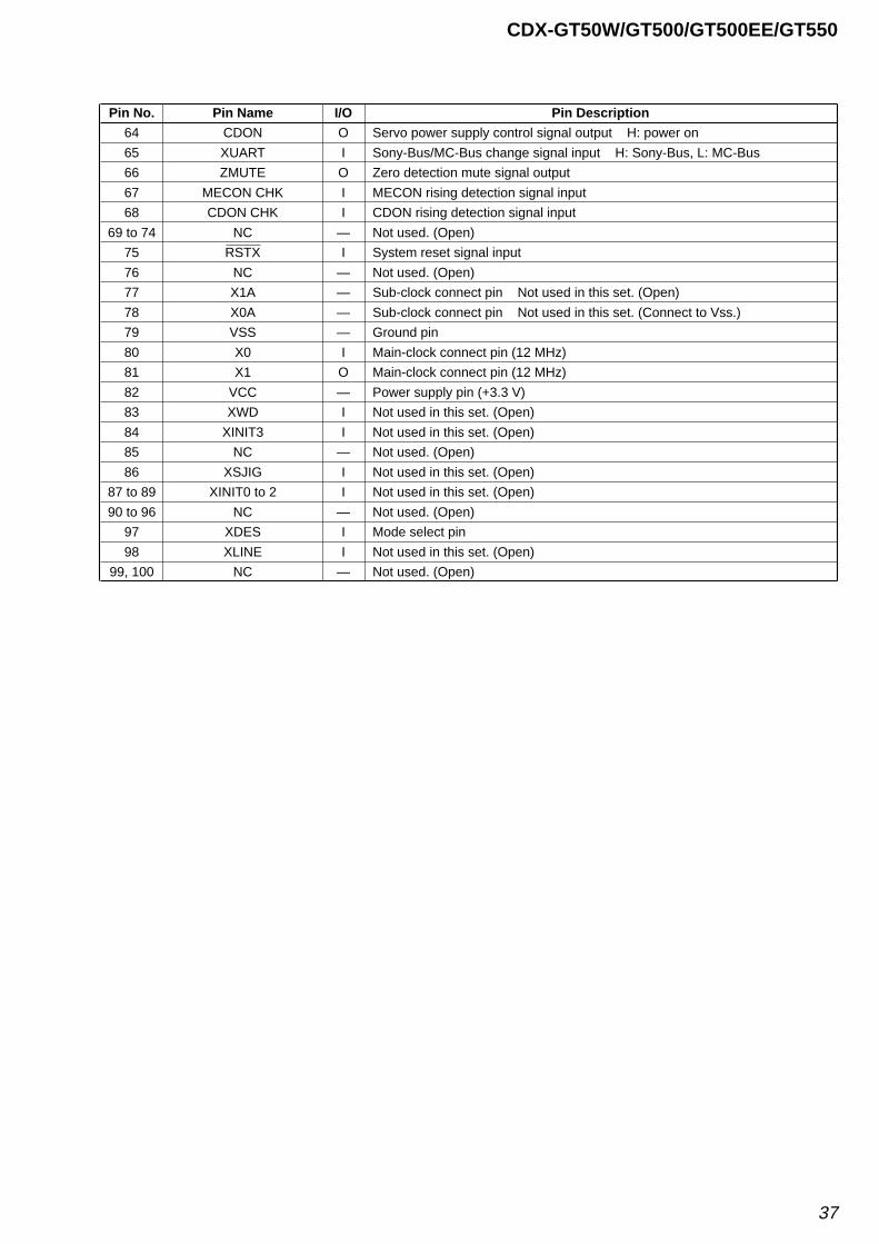
37
CDX-GT50W/GT500/GT500EE/GT550
Pin No. Pin Name I/O Pin Description
64 CDON O Servo power supply control signal output H: power on
65 XUART I Sony-Bus/MC-Bus change signal input H: Sony-Bus, L: MC-Bus
66 ZMUTE O Zero detection mute signal output
67 MECON CHK I MECON rising detection signal input
68 CDON CHK I CDON rising detection signal input
69 to 74 NC — Not used. (Open)
75 RSTX I System reset signal input
76 NC — Not used. (Open)
77 X1A — Sub-clock connect pin Not used in this set. (Open)
78 X0A — Sub-clock connect pin Not used in this set. (Connect to Vss.)
79 VSS — Ground pin
80 X0 I Main-clock connect pin (12 MHz)
81 X1 O Main-clock connect pin (12 MHz)
82 VCC — Power supply pin (+3.3 V)
83 XWD I Not used in this set. (Open)
84 XINIT3 I Not used in this set. (Open)
85 NC — Not used. (Open)
86 XSJIG I Not used in this set. (Open)
87 to 89 XINIT0 to 2 I Not used in this set. (Open)
90 to 96 NC — Not used. (Open)
97 XDES I Mode select pin
98 XLINE I Not used in this set. (Open)
99, 100 NC — Not used. (Open)
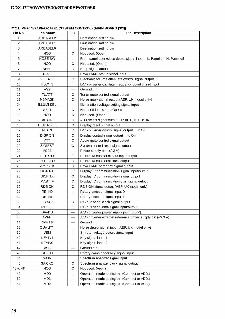
38
CDX-GT50W/GT500/GT500EE/GT550
IC711 MB90487APF-G-162E1 (SYSTEM CONTROL) (MAIN BOARD (3/3))Pin No. Pin Name I/O Pin Description
1 AREASEL2 I Destination setting pin
2 AREASEL1 I Destination setting pin
3 AREASEL0 I Destination setting pin
4 NCO O Not used. (Open)
5 NOSE SW I Front panel open/close detect signal input L: Panel on, H: Panel off
6 NCO O Not used. (Open)
7 BEEP O Beep signal output
8 DIAG I Power AMP status signal input
9 VOL ATT O Electronic volume attenuate control signal output
10 FSW IN I D/D converter oscillater frequency count signal input
11 VSS — Ground pin
12 TUATT O Tuner mute control signal output
13 NSMASK O Noise mask signal output (AEP, UK model only)
14 ILLUMI SEL I Illumination voltage setting signal input
15 SEL1 O Not used in this set. (Open)
16 NCO O Not used. (Open)
17 AUXIN O AUX select signal output L: AUX, H: BUS IN
18 DISP RSET O Display reset signal output
19 FL ON O D/D converter control signal output H: On
20 DISP ON O Display control signal output H: On
21 ATT O Audio mute control signal output
22 SYSRST O System control reset signal output
23 VCC5 — Power supply pin (+3.3 V)
24 EEP SIO I/O EEPROM bus serial data input/output
25 EEP CKO O EEPROM bus serial clock output
26 AMPSTB O Power AMP satandby signal output
27 DISP RX I/O Display IC communication signal input/output
28 DISP TX O Display IC communication signal output
29 MAST IF O Display IC communication start signal output
30 RDS ON O RDS ON signal output (AEP, UK model only)
31 RE IN0 I Rotary encoder signal input 0
32 RE IN1 I Rotary encoder signal input 1
33 I2C SCK O I2C bus serial clock signal output
34 I2C SIO I/O I2C bus serial data signal input/output
35 DAVDD — A/D converter power supply pin (+3.3 V)
36 AVRH — A/D converter external reference power supply pin (+3.3 V)
37 DAVSS — Ground pin
38 QUALITY I Noise detect signal input (AEP, UK model only)
39 VSM I S-meter voltage detect signal input
40 KEYIN1 I Key signal input 1
41 KEYIN0 I Key signal input 0
42 VSS — Ground pin
43 RC IN0 I Rotary commander key signal input
44 SA IN I Spectrum analyzer signal input
45 SA CKO O Spectrum analyzer clock signal output
46 to 48 NCO O Not used. (open)
49 MD0 I Operation mode setting pin (Connect to VDD.)
50 MD1 I Operation mode setting pin (Connect to VDD.)
51 MD2 I Operation mode setting pin (Connect to VSS.)
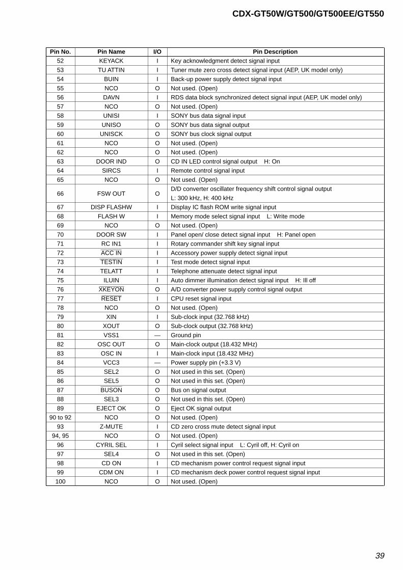
39
CDX-GT50W/GT500/GT500EE/GT550
Pin No. Pin Name I/O Pin Description
52 KEYACK I Key acknowledgment detect signal input
53 TU ATTIN I Tuner mute zero cross detect signal input (AEP, UK model only)
54 BUIN I Back-up power supply detect signal input
55 NCO O Not used. (Open)
56 DAVN I RDS data block synchronized detect signal input (AEP, UK model only)
57 NCO O Not used. (Open)
58 UNISI I SONY bus data signal input
59 UNISO O SONY bus data signal output
60 UNISCK O SONY bus clock signal output
61 NCO O Not used. (Open)
62 NCO O Not used. (Open)
63 DOOR IND O CD IN LED control signal output H: On
64 SIRCS I Remote control signal input
65 NCO O Not used. (Open)
66 FSW OUT OD/D converter oscillater frequency shift control signal output
L: 300 kHz, H: 400 kHz
67 DISP FLASHW I Display IC flash ROM write signal input
68 FLASH W I Memory mode select signal input L: Write mode
69 NCO O Not used. (Open)
70 DOOR SW I Panel open/ close detect signal input H: Panel open
71 RC IN1 I Rotary commander shift key signal input
72 ACC IN I Accessory power supply detect signal input
73 TESTIN I Test mode detect signal input
74 TELATT I Telephone attenuate detect signal input
75 ILUIN I Auto dimmer illumination detect signal input H: Ill off
76 XKEYON O A/D converter power supply control signal output
77 RESET I CPU reset signal input
78 NCO O Not used. (Open)
79 XIN I Sub-clock input (32.768 kHz)
80 XOUT O Sub-clock output (32.768 kHz)
81 VSS1 — Ground pin
82 OSC OUT O Main-clock output (18.432 MHz)
83 OSC IN I Main-clock input (18.432 MHz)
84 VCC3 — Power supply pin (+3.3 V)
85 SEL2 O Not used in this set. (Open)
86 SEL5 O Not used in this set. (Open)
87 BUSON O Bus on signal output
88 SEL3 O Not used in this set. (Open)
89 EJECT OK O Eject OK signal output
90 to 92 NCO O Not used. (Open)
93 Z-MUTE I CD zero cross mute detect signal input
94, 95 NCO O Not used. (Open)
96 CYRIL SEL I Cyril select signal input L: Cyril off, H: Cyril on
97 SEL4 O Not used in this set. (Open)
98 CD ON I CD mechanism power control request signal input
99 CDM ON I CD mechanism deck power control request signal input
100 NCO O Not used. (Open)
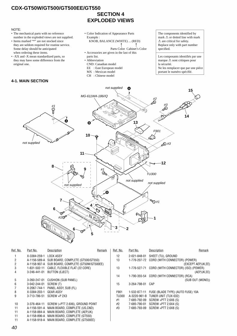
40
CDX-GT50W/GT500/GT500EE/GT550SECTION 4
EXPLODED VIEWS
Ref. No. Part No. Description Remark
4-1. MAIN SECTION
Ref. No. Part No. Description Remark
NOTE:• The mechanical parts with no reference
number in the exploded views are not supplied.• Items marked “*” are not stocked since
they are seldom required for routine service.Some delay should be anticipatedwhen ordering these items.
• -XX and -X mean standardized parts, sothey may have some difference from theoriginal one.
• Color Indication of Appearance PartsExample :
KNOB, BALANCE (WHITE) ... (RED)
Parts Color Cabinet’s Color• Accessories are given in the last of this
parts list.• Abbreviation
CND: Canadian modelEE : East European modelMX : Mexican modelCH : Chinese model
R R
1 X-3384-259-1 LOCK ASSY2 A-1156-589-A SUB BOARD, COMPLETE (GT500/GT550)2 A-1158-907-A SUB BOARD, COMPLETE (GT50W/GT500EE)3 1-831-502-11 CABLE, FLEXIBLE FLAT (22 CORE)4 3-246-441-01 BUTTON (EJECT)
5 3-260-247-01 CUSHION (SUB PANEL)6 3-042-244-01 SCREW (T)7 X-2067-744-1 PANEL ASSY, SUB (FL)8 X-3384-203-1 GEAR ASSY9 3-713-786-51 SCREW +P 2X3
10 3-376-464-11 SCREW (+PTT 2.6X6), GROUND POINT11 A-1156-591-A MAIN BOARD, COMPLETE (US,CND)11 A-1158-884-A MAIN BOARD, COMPLETE (AEP,UK)11 A-1158-896-A MAIN BOARD, COMPLETE (GT550)11 A-1158-918-A MAIN BOARD, COMPLETE (GT500EE)
12 2-021-848-01 SHEET (TU), GROUND13 1-776-207-72 CORD (WITH CONNECTOR) (POWER)
(EXCEPT AEP,UK,EE)13 1-776-527-71 CORD (WITH CONNECTOR) (ISO) (POWER)
(AEP,UK,EE)14 1-790-355-54 CORD (WITH CONNECTOR) (RCA)
(SUB OUT (MONO))15 3-264-798-01 CAP
F901 1-532-877-11 FUSE (BLADE TYPE) (AUTO FUSE) 10ATU300 A-3220-961-B TUNER UNIT (TUX-032)#1 7-685-792-09 SCREW +PTT 2.6X6 (S)#2 7-685-790-01 SCREW +PTT 2.6X4 (S)#3 7-685-793-09 SCREW +PTT 2.6X8 (S)
The components identified bymark 0 or dotted line with mark0 are critical for safety.Replace only with part numberspecified.
Les composants identifiés par unemarque 0 sont critiques pourla sécurité.Ne les remplacer que par une piéceportant le numéro spécifié.
F901
not suppliednot supplied
not supplied
not supplied
TU300
not supplied
#1
#1
#1
#3
#3
#2
#1
MG-611WA-186//Q
A
A
B
B
1
3 2
6
7
5
89
6
4
10
13
14
15
12
11
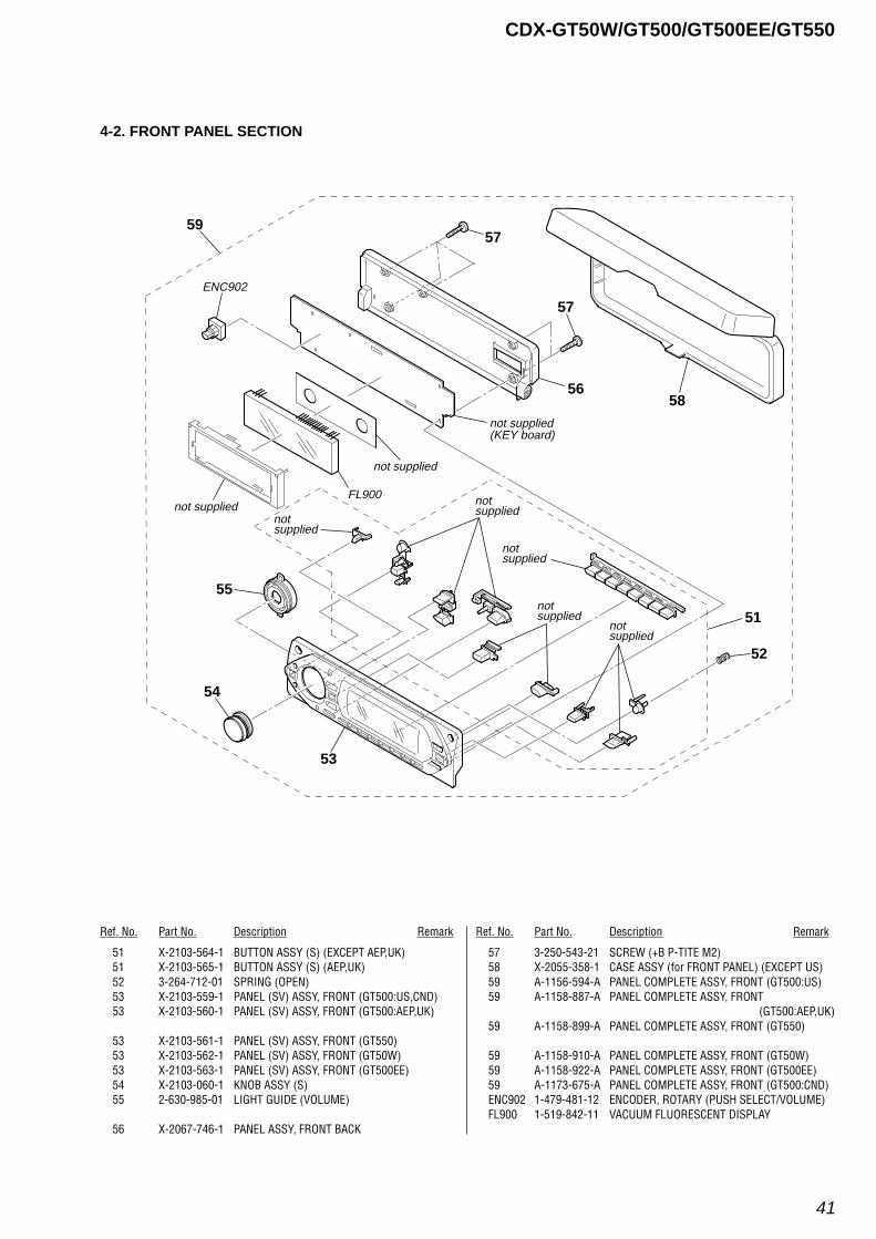
41
CDX-GT50W/GT500/GT500EE/GT550
4-2. FRONT PANEL SECTION
Ref. No. Part No. Description RemarkRef. No. Part No. Description Remark
51 X-2103-564-1 BUTTON ASSY (S) (EXCEPT AEP,UK)51 X-2103-565-1 BUTTON ASSY (S) (AEP,UK)52 3-264-712-01 SPRING (OPEN)53 X-2103-559-1 PANEL (SV) ASSY, FRONT (GT500:US,CND)53 X-2103-560-1 PANEL (SV) ASSY, FRONT (GT500:AEP,UK)
53 X-2103-561-1 PANEL (SV) ASSY, FRONT (GT550)53 X-2103-562-1 PANEL (SV) ASSY, FRONT (GT50W)53 X-2103-563-1 PANEL (SV) ASSY, FRONT (GT500EE)54 X-2103-060-1 KNOB ASSY (S)55 2-630-985-01 LIGHT GUIDE (VOLUME)
56 X-2067-746-1 PANEL ASSY, FRONT BACK
57 3-250-543-21 SCREW (+B P-TITE M2)58 X-2055-358-1 CASE ASSY (for FRONT PANEL) (EXCEPT US)59 A-1156-594-A PANEL COMPLETE ASSY, FRONT (GT500:US)59 A-1158-887-A PANEL COMPLETE ASSY, FRONT
(GT500:AEP,UK)59 A-1158-899-A PANEL COMPLETE ASSY, FRONT (GT550)
59 A-1158-910-A PANEL COMPLETE ASSY, FRONT (GT50W)59 A-1158-922-A PANEL COMPLETE ASSY, FRONT (GT500EE)59 A-1173-675-A PANEL COMPLETE ASSY, FRONT (GT500:CND)ENC902 1-479-481-12 ENCODER, ROTARY (PUSH SELECT/VOLUME)FL900 1-519-842-11 VACUUM FLUORESCENT DISPLAY
not supplied
not supplied
not supplied
not supplied
not supplied
not supplied
ENC902
not supplied(KEY board)
not suppliedFL900
51
52
53
54
55
56
57
57
58
59
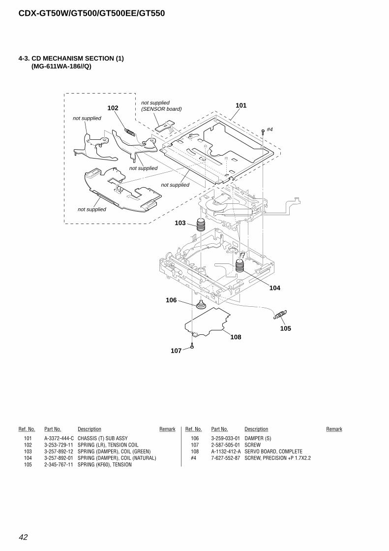
42
CDX-GT50W/GT500/GT500EE/GT550
4-3. CD MECHANISM SECTION (1)(MG-611WA-186//Q)
Ref. No. Part No. Description Remark Ref. No. Part No. Description Remark
101 A-3372-444-C CHASSIS (T) SUB ASSY102 3-253-729-11 SPRING (LR), TENSION COIL103 3-257-892-12 SPRING (DAMPER), COIL (GREEN)104 3-257-892-01 SPRING (DAMPER), COIL (NATURAL)105 2-345-767-11 SPRING (KF60), TENSION
106 3-259-033-01 DAMPER (S)107 2-587-505-01 SCREW108 A-1132-412-A SERVO BOARD, COMPLETE#4 7-627-552-87 SCREW, PRECISION +P 1.7X2.2
not supplied(SENSOR board)
not supplied
not supplied
#4
101102
103
104
105
106
107
108
not supplied
not supplied
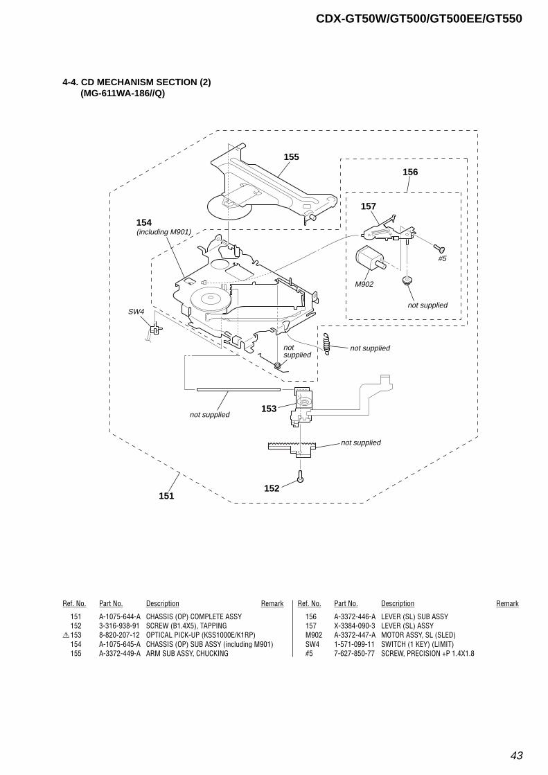
43
CDX-GT50W/GT500/GT500EE/GT550
Ref. No. Part No. Description Remark Ref. No. Part No. Description Remark
4-4. CD MECHANISM SECTION (2)(MG-611WA-186//Q)
151 A-1075-644-A CHASSIS (OP) COMPLETE ASSY152 3-316-938-91 SCREW (B1.4X5), TAPPING
0153 8-820-207-12 OPTICAL PICK-UP (KSS1000E/K1RP)154 A-1075-645-A CHASSIS (OP) SUB ASSY (including M901)155 A-3372-449-A ARM SUB ASSY, CHUCKING
156 A-3372-446-A LEVER (SL) SUB ASSY157 X-3384-090-3 LEVER (SL) ASSYM902 A-3372-447-A MOTOR ASSY, SL (SLED)SW4 1-571-099-11 SWITCH (1 KEY) (LIMIT)#5 7-627-850-77 SCREW, PRECISION +P 1.4X1.8
not supplied
SW4
not supplied
not suppliednot supplied
not supplied
#5
M902
151152
153
154(including M901)
155
156
157
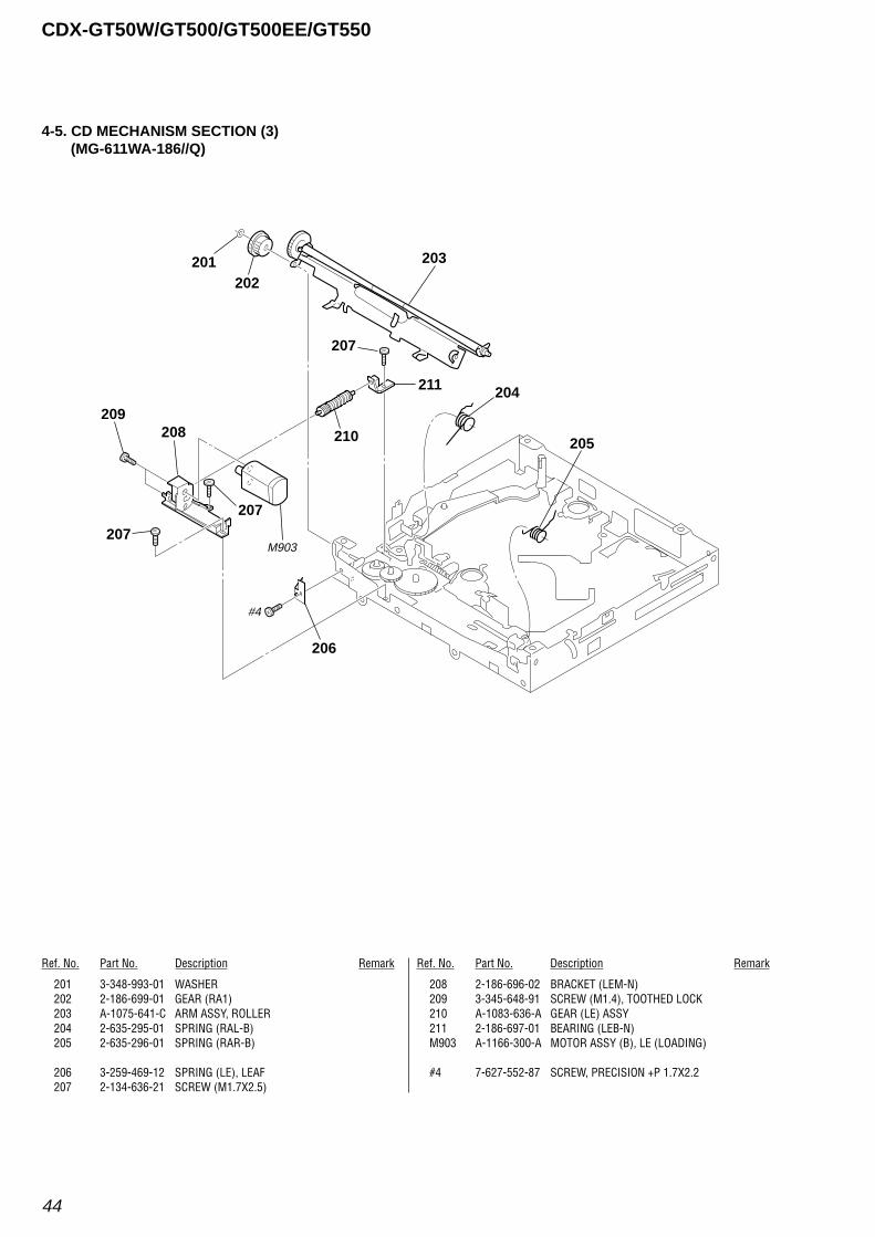
44
CDX-GT50W/GT500/GT500EE/GT550
Ref. No. Part No. Description Remark Ref. No. Part No. Description Remark
4-5. CD MECHANISM SECTION (3)(MG-611WA-186//Q)
201 3-348-993-01 WASHER202 2-186-699-01 GEAR (RA1)203 A-1075-641-C ARM ASSY, ROLLER204 2-635-295-01 SPRING (RAL-B)205 2-635-296-01 SPRING (RAR-B)
206 3-259-469-12 SPRING (LE), LEAF207 2-134-636-21 SCREW (M1.7X2.5)
208 2-186-696-02 BRACKET (LEM-N)209 3-345-648-91 SCREW (M1.4), TOOTHED LOCK210 A-1083-636-A GEAR (LE) ASSY211 2-186-697-01 BEARING (LEB-N)M903 A-1166-300-A MOTOR ASSY (B), LE (LOADING)
#4 7-627-552-87 SCREW, PRECISION +P 1.7X2.2
#4
M903
208 210
211
209
207
207
207
201202
203
204
205
206
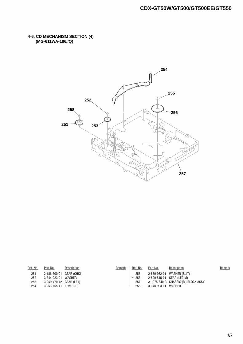
45
CDX-GT50W/GT500/GT500EE/GT550
Ref. No. Part No. Description Remark Ref. No. Part No. Description Remark
4-6. CD MECHANISM SECTION (4)(MG-611WA-186//Q)
251 2-186-700-01 GEAR (CHK1)252 3-344-223-01 WASHER253 3-259-470-12 GEAR (LE1)254 3-253-755-41 LEVER (D)
255 2-630-962-01 WASHER (SLIT)* 256 2-590-545-01 GEAR (LE2-M)
257 A-1075-640-B CHASSIS (M) BLOCK ASSY258 3-348-993-01 WASHER
251
252
254
255
256
257
253
258
46
CDX-GT50W/GT500/GT500EE/GT550SECTION 5
ELECTRICAL PARTS LIST
NOTE:• Due to standardization, replacements in
the parts list may be different from theparts specified in the diagrams or thecomponents used on the set.
• -XX and -X mean standardized parts, sothey may have some difference from theoriginal one.
• RESISTORSAll resistors are in ohms.METAL:Metal-film resistor.METAL OXIDE: Metal oxide-film resistor.F:nonflammable
• Items marked “*” are not stocked sincethey are seldom required for routine service.Some delay should be anticipatedwhen ordering these items.
• SEMICONDUCTORSIn each case, u : µ, for example:uA.. : µA.. uPA.. : µPA..uPB.. : µPB.. uPC..: µPC.. uPD.. : µPD..
• CAPACITORSuF : µF
• COILSuH : µH
• AbbreviationCND: Canadian modelEE : East European modelMX : Mexican modelCH : Chinese model
Ref. No. Part No. Description Remark Ref. No. Part No. Description Remark
KEY BOARD**********
< CAPACITOR >
C901 1-127-715-11 CERAMIC CHIP 0.22uF 10% 16VC903 1-163-021-11 CERAMIC CHIP 0.01uF 10% 50VC904 1-163-021-11 CERAMIC CHIP 0.01uF 10% 50VC970 1-107-826-11 CERAMIC CHIP 0.1uF 10% 16VC971 1-107-826-11 CERAMIC CHIP 0.1uF 10% 16V
C972 1-107-826-11 CERAMIC CHIP 0.1uF 10% 16VC973 1-125-837-11 CERAMIC CHIP 1uF 10% 6.3VC974 1-107-826-11 CERAMIC CHIP 0.1uF 10% 16VC975 1-162-913-11 CERAMIC CHIP 8PF 0.5PF 50VC976 1-162-913-11 CERAMIC CHIP 8PF 0.5PF 50V
C977 1-125-837-11 CERAMIC CHIP 1uF 10% 6.3VC978 1-100-623-11 CERAMIC CHIP 0.1uF 10% 100VC980 1-127-715-11 CERAMIC CHIP 0.22uF 10% 16VC981 1-107-826-11 CERAMIC CHIP 0.1uF 10% 16VC984 1-107-826-11 CERAMIC CHIP 0.1uF 10% 16V
C985 1-107-826-11 CERAMIC CHIP 0.1uF 10% 16V
< CONNECTOR >
CNP900 1-818-141-11 PLUG, CONNECTOR 20P
< DIODE >
D900 6-501-167-01 DIODE UDZW-TE17-5.1BD901 6-500-886-01 DIODE RSA6.1ENTRD903 6-500-886-01 DIODE RSA6.1ENTRD904 6-501-180-01 DIODE UDZW-TE17-18BD905 6-501-170-01 DIODE UDZW-TE17-6.8B
D906 6-501-170-01 DIODE UDZW-TE17-6.8BD909 6-500-886-01 DIODE RSA6.1ENTRD910 6-501-193-01 DIODE 1SS355WTE-17
< ROTARY ENCODER >
ENC902 1-479-481-12 ENCODER, ROTARY (PUSH SELECT/VOLUME)
< VACUUM FLUORESCENT DISPLAY >
FL900 1-519-842-11 VACUUM FLUORESCENT DISPLAY
< IC >
IC900 6-600-163-01 IC RS-770 (IR)IC901 6-806-178-01 IC uPD703263GC-103-8EA-A
IC902 6-707-877-01 IC TC74VHC32FT(EKJ)IC971 8-759-659-13 IC PST3428UL
< LED >
LED900 6-500-450-01 LED CL-195SR-CD-T(VOLUME ILLUMINATION)
(GT500/GT550)LED900 6-500-510-01 LED CL-195PG-CD-T
(VOLUME ILLUMINATION)(GT50W/GT500EE)
LED901 6-500-450-01 LED CL-195SR-CD-T(VOLUME ILLUMINATION)
(GT500/GT550)LED901 6-500-510-01 LED CL-195PG-CD-T
(VOLUME ILLUMINATION)(GT50W/GT500EE)
LED902 6-500-450-01 LED CL-195SR-CD-T(VOLUME ILLUMINATION)
(GT500/GT550)
LED902 6-500-510-01 LED CL-195PG-CD-T(VOLUME ILLUMINATION)
(GT50W/GT500EE)LED903 6-500-450-01 LED CL-195SR-CD-T
(VOLUME ILLUMINATION)(GT500/GT550)
LED903 6-500-510-01 LED CL-195PG-CD-T(VOLUME ILLUMINATION)
(GT50W/GT500EE)LED904 6-500-450-01 LED CL-195SR-CD-T (SOURCE)
(GT500/GT550)LED904 6-500-510-01 LED CL-195PG-CD-T (SOURCE)
(GT50W/GT500EE)
LED905 6-500-450-01 LED CL-195SR-CD-T (MODE) (GT500/GT550)LED905 6-500-510-01 LED CL-195PG-CD-T (MODE)
(GT50W/GT500EE)LED906 6-500-450-01 LED CL-195SR-CD-T (SCRL)
(GT500:US,CND/GT550)LED906 6-500-450-01 LED CL-195SR-CD-T (AF/TA)
(GT500:AEP,UK)LED906 6-500-510-01 LED CL-195PG-CD-T (SCRL)
(GT50W/GT500EE)
LED907 6-500-450-01 LED CL-195SR-CD-T (3) (GT500/GT550)LED907 6-500-510-01 LED CL-195PG-CD-T (3) (GT50W/GT500EE)LED908 6-500-450-01 LED CL-195SR-CD-T (2) (GT500/GT550)LED908 6-500-510-01 LED CL-195PG-CD-T (2) (GT50W/GT500EE)LED909 6-500-450-01 LED CL-195SR-CD-T (1) (GT500/GT550)
LED909 6-500-510-01 LED CL-195PG-CD-T (1) (GT50W/GT500EE)LED910 6-500-450-01 LED CL-195SR-CD-T (6) (GT500/GT550)
The components identified bymark 0 or dotted line with mark0 are critical for safety.Replace only with part numberspecified.
Les composants identifiés par unemarque 0 sont critiques pourla sécurité.Ne les remplacer que par une piéceportant le numéro spécifié.
When indicating parts by referencenumber, please include the board.
KEY
47
CDX-GT50W/GT500/GT500EE/GT550
Ref. No. Part No. Description Remark Ref. No. Part No. Description Remark
LED910 6-500-510-01 LED CL-195PG-CD-T (6) (GT50W/GT500EE)LED911 6-500-450-01 LED CL-195SR-CD-T (5) (GT500/GT550)LED911 6-500-510-01 LED CL-195PG-CD-T (5) (GT50W/GT500EE)LED912 6-500-450-01 LED CL-195SR-CD-T (4) (GT500/GT550)LED912 6-500-510-01 LED CL-195PG-CD-T (4) (GT50W/GT500EE)
LED913 6-500-450-01 LED CL-195SR-CD-T (DSO) (GT500/GT550)LED913 6-500-510-01 LED CL-195PG-CD-T (DSO)
(GT50W/GT500EE)LED914 6-500-450-01 LED CL-195SR-CD-T (IMAGE)
(GT500/GT550)LED914 6-500-510-01 LED CL-195PG-CD-T (IMAGE)
(GT50W/GT500EE)LED915 6-500-450-01 LED CL-195SR-CD-T (EQ3) (GT500/GT550)
LED915 6-500-510-01 LED CL-195PG-CD-T (EQ3)(GT50W/GT500EE)
< SWITCH >
LSW901 1-786-800-11 SWITCH, TACTILE (WITH LED) (OFF)(GT500/GT550)
LSW901 1-786-801-11 SWITCH, TACTILE (WITH LED) (OFF)(GT50W/GT500EE)
LSW902 1-786-800-11 SWITCH, TACTILE (WITH LED) (DSPL)(GT500/GT550)
LSW902 1-786-801-11 SWITCH, TACTILE (WITH LED) (DSPL)(GT50W/GT500EE)
LSW903 1-786-805-11 SWITCH, TACTILE (WITH LED) (SENS)(GT500:US,CND/GT550)
LSW903 1-786-805-11 SWITCH, TACTILE (WITH LED) (SENS/BTM)(GT500:AEP,UK)
LSW903 1-786-806-11 SWITCH, TACTILE (WITH LED) (SENS)(GT50W/GT500EE)
LSW904 1-786-805-11 SWITCH, TACTILE (WITH LED)(SEEK + > M)
(GT500/GT550)LSW904 1-786-806-11 SWITCH, TACTILE (WITH LED)
(SEEK + > M)(GT50W/GT500EE)
LSW905 1-786-805-11 SWITCH, TACTILE (WITH LED) (BTM/CAT)(GT500:US,CND)
LSW905 1-786-805-11 SWITCH, TACTILE (WITH LED) (PTY)(GT500:AEP,UK)
LSW905 1-786-805-11 SWITCH, TACTILE (WITH LED) (BTM) (GT550)LSW905 1-786-806-11 SWITCH, TACTILE (WITH LED) (BTM/CAT)
(GT50W)LSW905 1-786-806-11 SWITCH, TACTILE (WITH LED) (BTM)
(GT500EE)LSW907 1-786-805-11 SWITCH, TACTILE (WITH LED) (GP/ALBM +)
(GT500/GT550)
LSW907 1-786-806-11 SWITCH, TACTILE (WITH LED) (GP/ALBM +)(GT50W/GT500EE)
LSW908 1-786-805-11 SWITCH, TACTILE (WITH LED)(SEEK – . m)
(GT500/GT550)LSW908 1-786-806-11 SWITCH, TACTILE (WITH LED)
(SEEK – . m)(GT50W/GT500EE)
LSW909 1-786-805-11 SWITCH, TACTILE (WITH LED) (GP/ALBM –)(GT500/GT550)
LSW909 1-786-806-11 SWITCH, TACTILE (WITH LED) (GP/ALBM –)(GT50W/GT500EE)
< RESISTOR >
R900 1-216-815-11 METAL CHIP 330 5% 1/10WR901 1-216-815-11 METAL CHIP 330 5% 1/10WR902 1-216-864-11 SHORT CHIP 0R903 1-216-801-11 METAL CHIP 22 5% 1/10WR904 1-216-801-11 METAL CHIP 22 5% 1/10W
R905 1-216-797-11 METAL CHIP 10 5% 1/10WR906 1-216-797-11 METAL CHIP 10 5% 1/10WR907 1-216-801-11 METAL CHIP 22 5% 1/10WR908 1-216-801-11 METAL CHIP 22 5% 1/10WR909 1-216-801-11 METAL CHIP 22 5% 1/10W
R910 1-216-801-11 METAL CHIP 22 5% 1/10WR911 1-216-819-11 METAL CHIP 680 5% 1/10WR912 1-216-819-11 METAL CHIP 680 5% 1/10WR913 1-216-819-11 METAL CHIP 680 5% 1/10WR914 1-216-821-11 METAL CHIP 1K 5% 1/10W
R915 1-216-823-11 METAL CHIP 1.5K 5% 1/10WR916 1-216-823-11 METAL CHIP 1.5K 5% 1/10WR917 1-216-825-11 METAL CHIP 2.2K 5% 1/10WR918 1-216-827-11 METAL CHIP 3.3K 5% 1/10WR919 1-216-829-11 METAL CHIP 4.7K 5% 1/10W
R920 1-218-867-11 METAL CHIP 6.8K 0.5% 1/10WR921 1-216-809-11 METAL CHIP 100 5% 1/10WR922 1-216-809-11 METAL CHIP 100 5% 1/10WR923 1-216-819-11 METAL CHIP 680 5% 1/10WR924 1-216-819-11 METAL CHIP 680 5% 1/10W
R925 1-216-819-11 METAL CHIP 680 5% 1/10WR926 1-216-821-11 METAL CHIP 1K 5% 1/10WR927 1-216-823-11 METAL CHIP 1.5K 5% 1/10WR928 1-216-823-11 METAL CHIP 1.5K 5% 1/10WR929 1-216-825-11 METAL CHIP 2.2K 5% 1/10W
R930 1-216-827-11 METAL CHIP 3.3K 5% 1/10WR931 1-216-829-11 METAL CHIP 4.7K 5% 1/10WR932 1-218-867-11 METAL CHIP 6.8K 0.5% 1/10WR933 1-216-812-11 METAL CHIP 180 5% 1/10W
(GT50W/GT500EE)R933 1-216-813-11 METAL CHIP 220 5% 1/10W
(GT500/GT550)
R934 1-216-812-11 METAL CHIP 180 5% 1/10WR935 1-216-812-11 METAL CHIP 180 5% 1/10W
(GT50W/GT500EE)R935 1-216-813-11 METAL CHIP 220 5% 1/10W
(GT500/GT550)R936 1-216-810-11 METAL CHIP 120 5% 1/10W
(GT50W/GT500EE)R936 1-216-811-11 METAL CHIP 150 5% 1/10W
(GT500/GT550)
R937 1-216-809-11 METAL CHIP 100 5% 1/10W(GT50W/GT500EE)
R937 1-216-811-11 METAL CHIP 150 5% 1/10W(GT500/GT550)
R938 1-216-813-11 METAL CHIP 220 5% 1/10W(GT50W/GT500EE)
R938 1-216-814-11 METAL CHIP 270 5% 1/10W(GT500/GT550)
R939 1-216-810-11 METAL CHIP 120 5% 1/10W(GT50W/GT500EE)
R939 1-216-811-11 METAL CHIP 150 5% 1/10W(GT500/GT550)
KEY
48
CDX-GT50W/GT500/GT500EE/GT550
Ref. No. Part No. Description Remark Ref. No. Part No. Description Remark
R940 1-216-809-11 METAL CHIP 100 5% 1/10W(GT50W/GT500EE)
R940 1-216-811-11 METAL CHIP 150 5% 1/10W(GT500/GT550)
R942 1-216-813-11 METAL CHIP 220 5% 1/10W(GT50W/GT500EE)
R942 1-216-814-11 METAL CHIP 270 5% 1/10W(GT500/GT550)
R943 1-216-810-11 METAL CHIP 120 5% 1/10W(GT50W/GT500EE)
R943 1-216-811-11 METAL CHIP 150 5% 1/10W(GT500/GT550)
R944 1-216-809-11 METAL CHIP 100 5% 1/10W(GT50W/GT500EE)
R944 1-216-811-11 METAL CHIP 150 5% 1/10W(GT500/GT550)
R945 1-216-810-11 METAL CHIP 120 5% 1/10W(GT50W/GT500EE)
R945 1-216-811-11 METAL CHIP 150 5% 1/10W(GT500/GT550)
R946 1-216-809-11 METAL CHIP 100 5% 1/10W(GT50W/GT500EE)
R946 1-216-811-11 METAL CHIP 150 5% 1/10W(GT500/GT550)
R947 1-216-810-11 METAL CHIP 120 5% 1/10W(GT50W/GT500EE)
R947 1-216-811-11 METAL CHIP 150 5% 1/10W(GT500/GT550)
R948 1-216-809-11 METAL CHIP 100 5% 1/10W(GT50W/GT500EE)
R948 1-216-811-11 METAL CHIP 150 5% 1/10W(GT500/GT550)
R949 1-216-810-11 METAL CHIP 120 5% 1/10W(GT50W/GT500EE)
R949 1-216-811-11 METAL CHIP 150 5% 1/10W(GT500/GT550)
R950 1-216-809-11 METAL CHIP 100 5% 1/10W(GT50W/GT500EE)
R950 1-216-811-11 METAL CHIP 150 5% 1/10W(GT500/GT550)
R951 1-216-864-11 SHORT CHIP 0R952 1-216-864-11 SHORT CHIP 0R953 1-216-864-11 SHORT CHIP 0R954 1-216-813-11 METAL CHIP 220 5% 1/10W
(GT50W/GT500EE)R954 1-216-814-11 METAL CHIP 270 5% 1/10W
(GT500/GT550)
R955 1-216-813-11 METAL CHIP 220 5% 1/10W(GT50W/GT500EE)
R955 1-216-814-11 METAL CHIP 270 5% 1/10W(GT500/GT550)
R956 1-414-234-22 INDUCTOR, FERRITE BEADR957 1-216-864-11 SHORT CHIP 0R958 1-216-295-11 SHORT CHIP 0
R959 1-216-864-11 SHORT CHIP 0R960 1-216-864-11 SHORT CHIP 0R961 1-216-864-11 SHORT CHIP 0R962 1-216-797-11 METAL CHIP 10 5% 1/10WR963 1-216-801-11 METAL CHIP 22 5% 1/10W
R964 1-414-760-21 INDUCTOR, FERRITE BEADR965 1-414-760-21 INDUCTOR, FERRITE BEADR966 1-414-760-21 INDUCTOR, FERRITE BEAD
R967 1-414-760-21 INDUCTOR, FERRITE BEADR968 1-414-760-21 INDUCTOR, FERRITE BEADR969 1-216-833-11 METAL CHIP 10K 5% 1/10WR970 1-216-801-11 METAL CHIP 22 5% 1/10WR971 1-216-864-11 SHORT CHIP 0
R972 1-414-760-21 INDUCTOR, FERRITE BEADR973 1-216-801-11 METAL CHIP 22 5% 1/10WR974 1-414-760-21 INDUCTOR, FERRITE BEADR975 1-414-760-21 INDUCTOR, FERRITE BEADR976 1-414-760-21 INDUCTOR, FERRITE BEAD
R977 1-414-760-21 INDUCTOR, FERRITE BEADR979 1-414-760-21 INDUCTOR, FERRITE BEADR980 1-216-797-11 METAL CHIP 10 5% 1/10WR981 1-414-760-21 INDUCTOR, FERRITE BEADR982 1-414-235-22 INDUCTOR, FERRITE BEAD
R983 1-216-801-11 METAL CHIP 22 5% 1/10WR984 1-216-815-11 METAL CHIP 330 5% 1/10WR985 1-216-801-11 METAL CHIP 22 5% 1/10WR988 1-414-235-22 INDUCTOR, FERRITE BEADR989 1-216-841-11 METAL CHIP 47K 5% 1/10W
R990 1-216-845-11 METAL CHIP 100K 5% 1/10WR991 1-216-841-11 METAL CHIP 47K 5% 1/10WR992 1-216-009-11 RES-CHIP 22 5% 1/10WR993 1-216-845-11 METAL CHIP 100K 5% 1/10WR994 1-216-815-11 METAL CHIP 330 5% 1/10W
R995 1-414-760-21 INDUCTOR, FERRITE BEADR996 1-216-797-11 METAL CHIP 10 5% 1/10WR997 1-216-821-11 METAL CHIP 1K 5% 1/10WR998 1-216-009-11 RES-CHIP 22 5% 1/10WR999 1-216-841-11 METAL CHIP 47K 5% 1/10W
< SWITCH >
S908 1-786-653-21 SWITCH, TACTILE (DSO)S911 1-786-653-21 SWITCH, TACTILE (SOURCE)S912 1-786-653-21 SWITCH, TACTILE (EQ3)S913 1-786-653-21 SWITCH, TACTILE (6/PAUSE)S914 1-786-653-21 SWITCH, TACTILE (5/BBE MP)
S915 1-786-653-21 SWITCH, TACTILE (4/SHUF)S916 1-786-653-21 SWITCH, TACTILE (3/REP)S917 1-786-653-21 SWITCH, TACTILE (2)S918 1-786-653-21 SWITCH, TACTILE (1)S919 1-786-653-21 SWITCH, TACTILE (SCRL)
(GT50W/GT500:US,CND/GT500EE/GT550)
S919 1-786-653-21 SWITCH, TACTILE (AF/TA) (GT500:AEP,UK)S920 1-786-653-21 SWITCH, TACTILE (MODE)S921 1-786-653-21 SWITCH, TACTILE (IMAGE)
< VIBRATOR >
X901 1-813-487-21 VIBRATOR, CRYSTAL (5MHz)*************************************************************
KEY
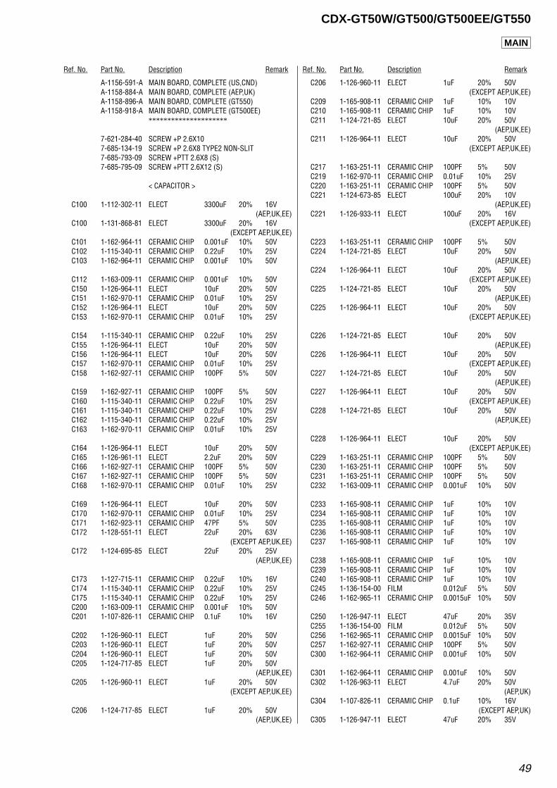
49
CDX-GT50W/GT500/GT500EE/GT550
Ref. No. Part No. Description Remark Ref. No. Part No. Description Remark
A-1156-591-A MAIN BOARD, COMPLETE (US,CND)A-1158-884-A MAIN BOARD, COMPLETE (AEP,UK)A-1158-896-A MAIN BOARD, COMPLETE (GT550)A-1158-918-A MAIN BOARD, COMPLETE (GT500EE)
*********************
7-621-284-40 SCREW +P 2.6X10⁷-685-134-19 SCREW +P 2.6X8 TYPE2 NON-SLIT7-685-793-09 SCREW +PTT 2.6X8 (S)7-685-795-09 SCREW +PTT 2.6X12 (S)
< CAPACITOR >
C100 1-112-302-11 ELECT 3300uF 20% 16V(AEP,UK,EE)
C100 1-131-868-81 ELECT 3300uF 20% 16V(EXCEPT AEP,UK,EE)
C101 1-162-964-11 CERAMIC CHIP 0.001uF 10% 50VC102 1-115-340-11 CERAMIC CHIP 0.22uF 10% 25VC103 1-162-964-11 CERAMIC CHIP 0.001uF 10% 50V
C112 1-163-009-11 CERAMIC CHIP 0.001uF 10% 50VC150 1-126-964-11 ELECT 10uF 20% 50VC151 1-162-970-11 CERAMIC CHIP 0.01uF 10% 25VC152 1-126-964-11 ELECT 10uF 20% 50VC153 1-162-970-11 CERAMIC CHIP 0.01uF 10% 25V
C154 1-115-340-11 CERAMIC CHIP 0.22uF 10% 25VC155 1-126-964-11 ELECT 10uF 20% 50VC156 1-126-964-11 ELECT 10uF 20% 50VC157 1-162-970-11 CERAMIC CHIP 0.01uF 10% 25VC158 1-162-927-11 CERAMIC CHIP 100PF 5% 50V
C159 1-162-927-11 CERAMIC CHIP 100PF 5% 50VC160 1-115-340-11 CERAMIC CHIP 0.22uF 10% 25VC161 1-115-340-11 CERAMIC CHIP 0.22uF 10% 25VC162 1-115-340-11 CERAMIC CHIP 0.22uF 10% 25VC163 1-162-970-11 CERAMIC CHIP 0.01uF 10% 25V
C164 1-126-964-11 ELECT 10uF 20% 50VC165 1-126-961-11 ELECT 2.2uF 20% 50VC166 1-162-927-11 CERAMIC CHIP 100PF 5% 50VC167 1-162-927-11 CERAMIC CHIP 100PF 5% 50VC168 1-162-970-11 CERAMIC CHIP 0.01uF 10% 25V
C169 1-126-964-11 ELECT 10uF 20% 50VC170 1-162-970-11 CERAMIC CHIP 0.01uF 10% 25VC171 1-162-923-11 CERAMIC CHIP 47PF 5% 50VC172 1-128-551-11 ELECT 22uF 20% 63V
(EXCEPT AEP,UK,EE)C172 1-124-695-85 ELECT 22uF 20% 25V
(AEP,UK,EE)
C173 1-127-715-11 CERAMIC CHIP 0.22uF 10% 16VC174 1-115-340-11 CERAMIC CHIP 0.22uF 10% 25VC175 1-115-340-11 CERAMIC CHIP 0.22uF 10% 25VC200 1-163-009-11 CERAMIC CHIP 0.001uF 10% 50VC201 1-107-826-11 CERAMIC CHIP 0.1uF 10% 16V
C202 1-126-960-11 ELECT 1uF 20% 50VC203 1-126-960-11 ELECT 1uF 20% 50VC204 1-126-960-11 ELECT 1uF 20% 50VC205 1-124-717-85 ELECT 1uF 20% 50V
(AEP,UK,EE)C205 1-126-960-11 ELECT 1uF 20% 50V
(EXCEPT AEP,UK,EE)
C206 1-124-717-85 ELECT 1uF 20% 50V(AEP,UK,EE)
C206 1-126-960-11 ELECT 1uF 20% 50V(EXCEPT AEP,UK,EE)
C209 1-165-908-11 CERAMIC CHIP 1uF 10% 10VC210 1-165-908-11 CERAMIC CHIP 1uF 10% 10VC211 1-124-721-85 ELECT 10uF 20% 50V
(AEP,UK,EE)C211 1-126-964-11 ELECT 10uF 20% 50V
(EXCEPT AEP,UK,EE)
C217 1-163-251-11 CERAMIC CHIP 100PF 5% 50VC219 1-162-970-11 CERAMIC CHIP 0.01uF 10% 25VC220 1-163-251-11 CERAMIC CHIP 100PF 5% 50VC221 1-124-673-85 ELECT 100uF 20% 10V
(AEP,UK,EE)C221 1-126-933-11 ELECT 100uF 20% 16V
(EXCEPT AEP,UK,EE)
C223 1-163-251-11 CERAMIC CHIP 100PF 5% 50VC224 1-124-721-85 ELECT 10uF 20% 50V
(AEP,UK,EE)C224 1-126-964-11 ELECT 10uF 20% 50V
(EXCEPT AEP,UK,EE)C225 1-124-721-85 ELECT 10uF 20% 50V
(AEP,UK,EE)C225 1-126-964-11 ELECT 10uF 20% 50V
(EXCEPT AEP,UK,EE)
C226 1-124-721-85 ELECT 10uF 20% 50V(AEP,UK,EE)
C226 1-126-964-11 ELECT 10uF 20% 50V(EXCEPT AEP,UK,EE)
C227 1-124-721-85 ELECT 10uF 20% 50V(AEP,UK,EE)
C227 1-126-964-11 ELECT 10uF 20% 50V(EXCEPT AEP,UK,EE)
C228 1-124-721-85 ELECT 10uF 20% 50V(AEP,UK,EE)
C228 1-126-964-11 ELECT 10uF 20% 50V(EXCEPT AEP,UK,EE)
C229 1-163-251-11 CERAMIC CHIP 100PF 5% 50VC230 1-163-251-11 CERAMIC CHIP 100PF 5% 50VC231 1-163-251-11 CERAMIC CHIP 100PF 5% 50VC232 1-163-009-11 CERAMIC CHIP 0.001uF 10% 50V
C233 1-165-908-11 CERAMIC CHIP 1uF 10% 10VC234 1-165-908-11 CERAMIC CHIP 1uF 10% 10VC235 1-165-908-11 CERAMIC CHIP 1uF 10% 10VC236 1-165-908-11 CERAMIC CHIP 1uF 10% 10VC237 1-165-908-11 CERAMIC CHIP 1uF 10% 10V
C238 1-165-908-11 CERAMIC CHIP 1uF 10% 10VC239 1-165-908-11 CERAMIC CHIP 1uF 10% 10VC240 1-165-908-11 CERAMIC CHIP 1uF 10% 10VC245 1-136-154-00 FILM 0.012uF 5% 50VC246 1-162-965-11 CERAMIC CHIP 0.0015uF 10% 50V
C250 1-126-947-11 ELECT 47uF 20% 35VC255 1-136-154-00 FILM 0.012uF 5% 50VC256 1-162-965-11 CERAMIC CHIP 0.0015uF 10% 50VC257 1-162-927-11 CERAMIC CHIP 100PF 5% 50VC300 1-162-964-11 CERAMIC CHIP 0.001uF 10% 50V
C301 1-162-964-11 CERAMIC CHIP 0.001uF 10% 50VC302 1-126-963-11 ELECT 4.7uF 20% 50V
(AEP,UK)C304 1-107-826-11 CERAMIC CHIP 0.1uF 10% 16V
(EXCEPT AEP,UK)C305 1-126-947-11 ELECT 47uF 20% 35V
MAIN
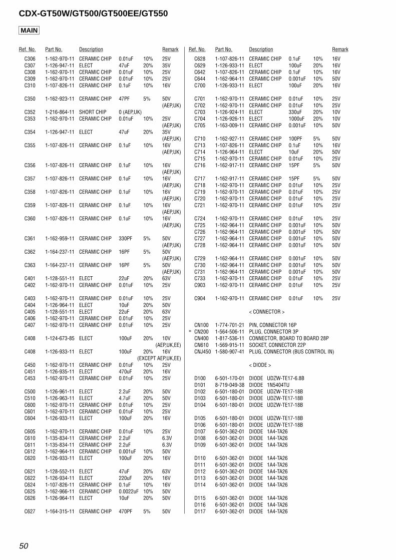
50
CDX-GT50W/GT500/GT500EE/GT550
Ref. No. Part No. Description Remark Ref. No. Part No. Description Remark
C306 1-162-970-11 CERAMIC CHIP 0.01uF 10% 25VC307 1-126-947-11 ELECT 47uF 20% 35VC308 1-162-970-11 CERAMIC CHIP 0.01uF 10% 25VC309 1-162-970-11 CERAMIC CHIP 0.01uF 10% 25VC310 1-107-826-11 CERAMIC CHIP 0.1uF 10% 16V
C350 1-162-923-11 CERAMIC CHIP 47PF 5% 50V(AEP,UK)
C352 1-216-864-11 SHORT CHIP 0 (AEP,UK)C353 1-162-970-11 CERAMIC CHIP 0.01uF 10% 25V
(AEP,UK)C354 1-126-947-11 ELECT 47uF 20% 35V
(AEP,UK)C355 1-107-826-11 CERAMIC CHIP 0.1uF 10% 16V
(AEP,UK)
C356 1-107-826-11 CERAMIC CHIP 0.1uF 10% 16V(AEP,UK)
C357 1-107-826-11 CERAMIC CHIP 0.1uF 10% 16V(AEP,UK)
C358 1-107-826-11 CERAMIC CHIP 0.1uF 10% 16V(AEP,UK)
C359 1-107-826-11 CERAMIC CHIP 0.1uF 10% 16V(AEP,UK)
C360 1-107-826-11 CERAMIC CHIP 0.1uF 10% 16V(AEP,UK)
C361 1-162-959-11 CERAMIC CHIP 330PF 5% 50V(AEP,UK)
C362 1-164-237-11 CERAMIC CHIP 16PF 5% 50V(AEP,UK)
C363 1-164-237-11 CERAMIC CHIP 16PF 5% 50V(AEP,UK)
C401 1-128-551-11 ELECT 22uF 20% 63VC402 1-162-970-11 CERAMIC CHIP 0.01uF 10% 25V
C403 1-162-970-11 CERAMIC CHIP 0.01uF 10% 25VC404 1-126-964-11 ELECT 10uF 20% 50VC405 1-128-551-11 ELECT 22uF 20% 63VC406 1-162-970-11 CERAMIC CHIP 0.01uF 10% 25VC407 1-162-970-11 CERAMIC CHIP 0.01uF 10% 25V
C408 1-124-673-85 ELECT 100uF 20% 10V(AEP,UK,EE)
C408 1-126-933-11 ELECT 100uF 20% 16V(EXCEPT AEP,UK,EE)
C450 1-162-970-11 CERAMIC CHIP 0.01uF 10% 25VC451 1-126-935-11 ELECT 470uF 20% 16VC453 1-162-970-11 CERAMIC CHIP 0.01uF 10% 25V
C500 1-126-961-11 ELECT 2.2uF 20% 50VC510 1-126-963-11 ELECT 4.7uF 20% 50VC600 1-162-970-11 CERAMIC CHIP 0.01uF 10% 25VC601 1-162-970-11 CERAMIC CHIP 0.01uF 10% 25VC604 1-126-933-11 ELECT 100uF 20% 16V
C605 1-162-970-11 CERAMIC CHIP 0.01uF 10% 25VC610 1-135-834-11 CERAMIC CHIP 2.2uF 6.3VC611 1-135-834-11 CERAMIC CHIP 2.2uF 6.3VC612 1-162-964-11 CERAMIC CHIP 0.001uF 10% 50VC620 1-126-933-11 ELECT 100uF 20% 16V
C621 1-128-552-11 ELECT 47uF 20% 63VC622 1-126-934-11 ELECT 220uF 20% 16VC624 1-107-826-11 CERAMIC CHIP 0.1uF 10% 16VC625 1-162-966-11 CERAMIC CHIP 0.0022uF 10% 50VC626 1-126-964-11 ELECT 10uF 20% 50V
C627 1-164-315-11 CERAMIC CHIP 470PF 5% 50V
C628 1-107-826-11 CERAMIC CHIP 0.1uF 10% 16VC629 1-126-933-11 ELECT 100uF 20% 16VC642 1-107-826-11 CERAMIC CHIP 0.1uF 10% 16VC644 1-162-964-11 CERAMIC CHIP 0.001uF 10% 50VC700 1-126-933-11 ELECT 100uF 20% 16V
C701 1-162-970-11 CERAMIC CHIP 0.01uF 10% 25VC702 1-162-970-11 CERAMIC CHIP 0.01uF 10% 25VC703 1-126-924-11 ELECT 330uF 20% 10VC704 1-126-926-11 ELECT 1000uF 20% 10VC705 1-163-009-11 CERAMIC CHIP 0.001uF 10% 50V
C710 1-162-927-11 CERAMIC CHIP 100PF 5% 50VC713 1-107-826-11 CERAMIC CHIP 0.1uF 10% 16VC714 1-126-964-11 ELECT 10uF 20% 50VC715 1-162-970-11 CERAMIC CHIP 0.01uF 10% 25VC716 1-162-917-11 CERAMIC CHIP 15PF 5% 50V
C717 1-162-917-11 CERAMIC CHIP 15PF 5% 50VC718 1-162-970-11 CERAMIC CHIP 0.01uF 10% 25VC719 1-162-970-11 CERAMIC CHIP 0.01uF 10% 25VC720 1-162-970-11 CERAMIC CHIP 0.01uF 10% 25VC721 1-162-970-11 CERAMIC CHIP 0.01uF 10% 25V
C724 1-162-970-11 CERAMIC CHIP 0.01uF 10% 25VC725 1-162-964-11 CERAMIC CHIP 0.001uF 10% 50VC726 1-162-964-11 CERAMIC CHIP 0.001uF 10% 50VC727 1-162-964-11 CERAMIC CHIP 0.001uF 10% 50VC728 1-162-964-11 CERAMIC CHIP 0.001uF 10% 50V
C729 1-162-964-11 CERAMIC CHIP 0.001uF 10% 50VC730 1-162-964-11 CERAMIC CHIP 0.001uF 10% 50VC731 1-162-964-11 CERAMIC CHIP 0.001uF 10% 50VC733 1-162-970-11 CERAMIC CHIP 0.01uF 10% 25VC903 1-162-970-11 CERAMIC CHIP 0.01uF 10% 25V
C904 1-162-970-11 CERAMIC CHIP 0.01uF 10% 25V
< CONNECTOR >
CN100 1-774-701-21 PIN, CONNECTOR 16P* CN200 1-564-506-11 PLUG, CONNECTOR 3P
CN400 1-817-536-11 CONNECTOR, BOARD TO BOARD 28PCN610 1-569-915-11 SOCKET, CONNECTOR 22PCNJ450 1-580-907-41 PLUG, CONNECTOR (BUS CONTROL IN)
< DIODE >
D100 6-501-170-01 DIODE UDZW-TE17-6.8BD101 8-719-049-38 DIODE 1N5404TUD102 6-501-180-01 DIODE UDZW-TE17-18BD103 6-501-180-01 DIODE UDZW-TE17-18BD104 6-501-180-01 DIODE UDZW-TE17-18B
D105 6-501-180-01 DIODE UDZW-TE17-18BD106 6-501-180-01 DIODE UDZW-TE17-18BD107 6-501-362-01 DIODE 1A4-TA26D108 6-501-362-01 DIODE 1A4-TA26D109 6-501-362-01 DIODE 1A4-TA26
D110 6-501-362-01 DIODE 1A4-TA26D111 6-501-362-01 DIODE 1A4-TA26D112 6-501-362-01 DIODE 1A4-TA26D113 6-501-362-01 DIODE 1A4-TA26D114 6-501-362-01 DIODE 1A4-TA26
D115 6-501-362-01 DIODE 1A4-TA26D116 6-501-362-01 DIODE 1A4-TA26D117 6-501-362-01 DIODE 1A4-TA26
MAIN
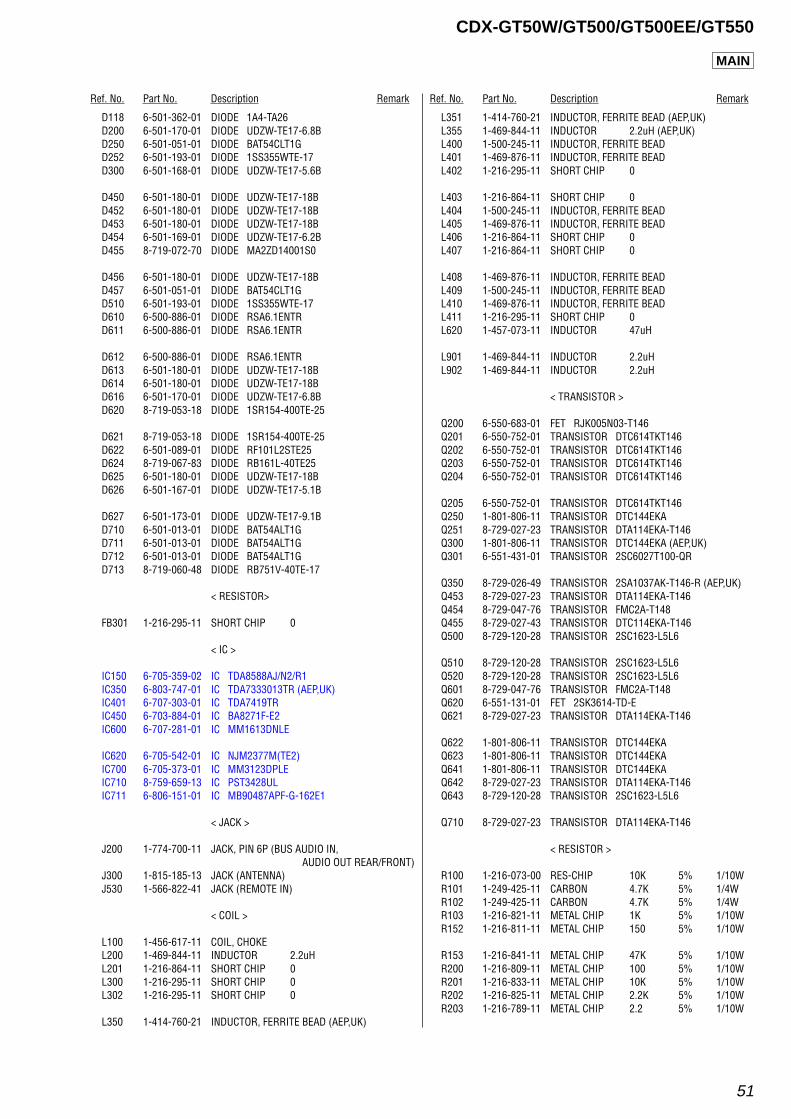
51
CDX-GT50W/GT500/GT500EE/GT550
Ref. No. Part No. Description Remark Ref. No. Part No. Description Remark
D118 6-501-362-01 DIODE 1A4-TA26D200 6-501-170-01 DIODE UDZW-TE17-6.8BD250 6-501-051-01 DIODE BAT54CLT1GD252 6-501-193-01 DIODE 1SS355WTE-17D300 6-501-168-01 DIODE UDZW-TE17-5.6B
D450 6-501-180-01 DIODE UDZW-TE17-18BD452 6-501-180-01 DIODE UDZW-TE17-18BD453 6-501-180-01 DIODE UDZW-TE17-18BD454 6-501-169-01 DIODE UDZW-TE17-6.2BD455 8-719-072-70 DIODE MA2ZD14001S0
D456 6-501-180-01 DIODE UDZW-TE17-18BD457 6-501-051-01 DIODE BAT54CLT1GD510 6-501-193-01 DIODE 1SS355WTE-17D610 6-500-886-01 DIODE RSA6.1ENTRD611 6-500-886-01 DIODE RSA6.1ENTR
D612 6-500-886-01 DIODE RSA6.1ENTRD613 6-501-180-01 DIODE UDZW-TE17-18BD614 6-501-180-01 DIODE UDZW-TE17-18BD616 6-501-170-01 DIODE UDZW-TE17-6.8BD620 8-719-053-18 DIODE 1SR154-400TE-25
D621 8-719-053-18 DIODE 1SR154-400TE-25D622 6-501-089-01 DIODE RF101L2STE25D624 8-719-067-83 DIODE RB161L-40TE25D625 6-501-180-01 DIODE UDZW-TE17-18BD626 6-501-167-01 DIODE UDZW-TE17-5.1B
D627 6-501-173-01 DIODE UDZW-TE17-9.1BD710 6-501-013-01 DIODE BAT54ALT1GD711 6-501-013-01 DIODE BAT54ALT1GD712 6-501-013-01 DIODE BAT54ALT1GD713 8-719-060-48 DIODE RB751V-40TE-17
< RESISTOR>
FB301 1-216-295-11 SHORT CHIP 0
< IC >
IC150 6-705-359-02 IC TDA8588AJ/N2/R1IC350 6-803-747-01 IC TDA7333013TR (AEP,UK)IC401 6-707-303-01 IC TDA7419TRIC450 6-703-884-01 IC BA8271F-E2IC600 6-707-281-01 IC MM1613DNLE
IC620 6-705-542-01 IC NJM2377M(TE2)IC700 6-705-373-01 IC MM3123DPLEIC710 8-759-659-13 IC PST3428ULIC711 6-806-151-01 IC MB90487APF-G-162E1
< JACK >
J200 1-774-700-11 JACK, PIN 6P (BUS AUDIO IN,AUDIO OUT REAR/FRONT)
J300 1-815-185-13 JACK (ANTENNA)J530 1-566-822-41 JACK (REMOTE IN)
< COIL >
L100 1-456-617-11 COIL, CHOKEL200 1-469-844-11 INDUCTOR 2.2uHL201 1-216-864-11 SHORT CHIP 0L300 1-216-295-11 SHORT CHIP 0L302 1-216-295-11 SHORT CHIP 0
L350 1-414-760-21 INDUCTOR, FERRITE BEAD (AEP,UK)
L351 1-414-760-21 INDUCTOR, FERRITE BEAD (AEP,UK)L355 1-469-844-11 INDUCTOR 2.2uH (AEP,UK)L400 1-500-245-11 INDUCTOR, FERRITE BEADL401 1-469-876-11 INDUCTOR, FERRITE BEADL402 1-216-295-11 SHORT CHIP 0
L403 1-216-864-11 SHORT CHIP 0L404 1-500-245-11 INDUCTOR, FERRITE BEADL405 1-469-876-11 INDUCTOR, FERRITE BEADL406 1-216-864-11 SHORT CHIP 0L407 1-216-864-11 SHORT CHIP 0
L408 1-469-876-11 INDUCTOR, FERRITE BEADL409 1-500-245-11 INDUCTOR, FERRITE BEADL410 1-469-876-11 INDUCTOR, FERRITE BEADL411 1-216-295-11 SHORT CHIP 0L620 1-457-073-11 INDUCTOR 47uH
L901 1-469-844-11 INDUCTOR 2.2uHL902 1-469-844-11 INDUCTOR 2.2uH
< TRANSISTOR >
Q200 6-550-683-01 FET RJK005N03-T146Q201 6-550-752-01 TRANSISTOR DTC614TKT146Q202 6-550-752-01 TRANSISTOR DTC614TKT146Q203 6-550-752-01 TRANSISTOR DTC614TKT146Q204 6-550-752-01 TRANSISTOR DTC614TKT146
Q205 6-550-752-01 TRANSISTOR DTC614TKT146Q250 1-801-806-11 TRANSISTOR DTC144EKAQ251 8-729-027-23 TRANSISTOR DTA114EKA-T146Q300 1-801-806-11 TRANSISTOR DTC144EKA (AEP,UK)Q301 6-551-431-01 TRANSISTOR 2SC6027T100-QR
Q350 8-729-026-49 TRANSISTOR 2SA1037AK-T146-R (AEP,UK)Q453 8-729-027-23 TRANSISTOR DTA114EKA-T146Q454 8-729-047-76 TRANSISTOR FMC2A-T148Q455 8-729-027-43 TRANSISTOR DTC114EKA-T146Q500 8-729-120-28 TRANSISTOR 2SC1623-L5L6
Q510 8-729-120-28 TRANSISTOR 2SC1623-L5L6Q520 8-729-120-28 TRANSISTOR 2SC1623-L5L6Q601 8-729-047-76 TRANSISTOR FMC2A-T148Q620 6-551-131-01 FET 2SK3614-TD-EQ621 8-729-027-23 TRANSISTOR DTA114EKA-T146
Q622 1-801-806-11 TRANSISTOR DTC144EKAQ623 1-801-806-11 TRANSISTOR DTC144EKAQ641 1-801-806-11 TRANSISTOR DTC144EKAQ642 8-729-027-23 TRANSISTOR DTA114EKA-T146Q643 8-729-120-28 TRANSISTOR 2SC1623-L5L6
Q710 8-729-027-23 TRANSISTOR DTA114EKA-T146
< RESISTOR >
R100 1-216-073-00 RES-CHIP 10K 5% 1/10WR101 1-249-425-11 CARBON 4.7K 5% 1/4WR102 1-249-425-11 CARBON 4.7K 5% 1/4WR103 1-216-821-11 METAL CHIP 1K 5% 1/10WR152 1-216-811-11 METAL CHIP 150 5% 1/10W
R153 1-216-841-11 METAL CHIP 47K 5% 1/10WR200 1-216-809-11 METAL CHIP 100 5% 1/10WR201 1-216-833-11 METAL CHIP 10K 5% 1/10WR202 1-216-825-11 METAL CHIP 2.2K 5% 1/10WR203 1-216-789-11 METAL CHIP 2.2 5% 1/10W
MAIN

52
CDX-GT50W/GT500/GT500EE/GT550
R204 1-216-825-11 METAL CHIP 2.2K 5% 1/10WR205 1-216-833-11 METAL CHIP 10K 5% 1/10WR206 1-216-833-11 METAL CHIP 10K 5% 1/10WR207 1-216-809-11 METAL CHIP 100 5% 1/10WR208 1-216-809-11 METAL CHIP 100 5% 1/10W
R209 1-216-809-11 METAL CHIP 100 5% 1/10WR210 1-216-809-11 METAL CHIP 100 5% 1/10WR214 1-216-809-11 METAL CHIP 100 5% 1/10WR215 1-216-809-11 METAL CHIP 100 5% 1/10WR216 1-216-809-11 METAL CHIP 100 5% 1/10W
R217 1-216-809-11 METAL CHIP 100 5% 1/10WR218 1-216-809-11 METAL CHIP 100 5% 1/10WR220 1-216-809-11 METAL CHIP 100 5% 1/10WR221 1-216-809-11 METAL CHIP 100 5% 1/10WR222 1-216-809-11 METAL CHIP 100 5% 1/10W
R223 1-216-809-11 METAL CHIP 100 5% 1/10WR224 1-216-809-11 METAL CHIP 100 5% 1/10WR225 1-216-833-11 METAL CHIP 10K 5% 1/10WR226 1-216-833-11 METAL CHIP 10K 5% 1/10WR227 1-216-833-11 METAL CHIP 10K 5% 1/10W
R228 1-216-833-11 METAL CHIP 10K 5% 1/10WR229 1-216-833-11 METAL CHIP 10K 5% 1/10WR230 1-216-864-11 SHORT CHIP 0R231 1-216-864-11 SHORT CHIP 0R232 1-216-864-11 SHORT CHIP 0
R233 1-216-864-11 SHORT CHIP 0R245 1-216-833-11 METAL CHIP 10K 5% 1/10WR246 1-216-833-11 METAL CHIP 10K 5% 1/10WR251 1-216-805-11 METAL CHIP 47 5% 1/10WR255 1-216-833-11 METAL CHIP 10K 5% 1/10W
R256 1-216-833-11 METAL CHIP 10K 5% 1/10WR262 1-216-864-11 SHORT CHIP 0R300 1-216-843-11 METAL CHIP 68K 5% 1/10WR301 1-216-839-11 METAL CHIP 33K 5% 1/10WR302 1-216-809-11 METAL CHIP 100 5% 1/10W
(AEP,UK)
R303 1-216-843-11 METAL CHIP 68K 5% 1/10WR304 1-216-839-11 METAL CHIP 33K 5% 1/10WR305 1-216-843-11 METAL CHIP 68K 5% 1/10WR306 1-216-839-11 METAL CHIP 33K 5% 1/10W
(AEP,UK)R307 1-414-760-21 INDUCTOR, FERRITE BEAD
R308 1-414-760-21 INDUCTOR, FERRITE BEADR309 1-414-760-21 INDUCTOR, FERRITE BEADR310 1-414-760-21 INDUCTOR, FERRITE BEADR311 1-216-821-11 METAL CHIP 1K 5% 1/10WR350 1-216-821-11 METAL CHIP 1K 5% 1/10W
(AEP,UK)
R351 1-216-833-11 METAL CHIP 10K 5% 1/10W(AEP,UK)
R352 1-216-797-11 METAL CHIP 10 5% 1/10W(AEP,UK)
R353 1-216-797-11 METAL CHIP 10 5% 1/10W(AEP,UK)
R354 1-216-845-11 METAL CHIP 100K 5% 1/10W(AEP,UK)
R355 1-216-801-11 METAL CHIP 22 5% 1/10W(AEP,UK)
Ref. No. Part No. Description Remark
R356 1-216-864-11 SHORT CHIP 0 (AEP,UK)R357 1-216-864-11 SHORT CHIP 0 (AEP,UK)R358 1-216-797-11 METAL CHIP 10 5% 1/10W
(AEP,UK)R359 1-216-864-11 SHORT CHIP 0 (AEP,UK)R400 1-216-864-11 SHORT CHIP 0
R401 1-216-801-11 METAL CHIP 22 5% 1/10WR402 1-216-801-11 METAL CHIP 22 5% 1/10WR403 1-216-801-11 METAL CHIP 22 5% 1/10WR404 1-216-801-11 METAL CHIP 22 5% 1/10WR405 1-216-801-11 METAL CHIP 22 5% 1/10W
R406 1-216-864-11 SHORT CHIP 0R407 1-216-864-11 SHORT CHIP 0R450 1-216-864-11 SHORT CHIP 0R453 1-216-864-11 SHORT CHIP 0R455 1-216-864-11 SHORT CHIP 0
R456 1-216-829-11 METAL CHIP 4.7K 5% 1/10WR457 1-216-821-11 METAL CHIP 1K 5% 1/10WR458 1-216-821-11 METAL CHIP 1K 5% 1/10WR459 1-216-835-11 METAL CHIP 15K 5% 1/10WR461 1-216-821-11 METAL CHIP 1K 5% 1/10W
R500 1-216-841-11 METAL CHIP 47K 5% 1/10WR501 1-216-841-11 METAL CHIP 47K 5% 1/10WR502 1-216-829-11 METAL CHIP 4.7K 5% 1/10WR510 1-216-845-11 METAL CHIP 100K 5% 1/10WR511 1-216-837-11 METAL CHIP 22K 5% 1/10W
R520 1-216-841-11 METAL CHIP 47K 5% 1/10WR521 1-216-833-11 METAL CHIP 10K 5% 1/10WR522 1-216-833-11 METAL CHIP 10K 5% 1/10WR530 1-216-809-11 METAL CHIP 100 5% 1/10WR531 1-216-809-11 METAL CHIP 100 5% 1/10W
R532 1-216-864-11 SHORT CHIP 0R605 1-216-029-00 RES-CHIP 150 5% 1/10WR606 1-216-029-00 RES-CHIP 150 5% 1/10WR607 1-216-029-00 RES-CHIP 150 5% 1/10WR610 1-216-809-11 METAL CHIP 100 5% 1/10W
R611 1-216-809-11 METAL CHIP 100 5% 1/10WR612 1-216-809-11 METAL CHIP 100 5% 1/10WR613 1-216-809-11 METAL CHIP 100 5% 1/10WR614 1-216-809-11 METAL CHIP 100 5% 1/10WR615 1-216-809-11 METAL CHIP 100 5% 1/10W
R616 1-216-809-11 METAL CHIP 100 5% 1/10WR617 1-216-809-11 METAL CHIP 100 5% 1/10WR618 1-216-809-11 METAL CHIP 100 5% 1/10WR619 1-216-841-11 METAL CHIP 47K 5% 1/10WR620 1-216-841-11 METAL CHIP 47K 5% 1/10W
R621 1-216-841-11 METAL CHIP 47K 5% 1/10WR622 1-218-863-11 METAL CHIP 4.7K 0.5% 1/10WR623 1-218-895-11 METAL CHIP 100K 0.5% 1/10WR624 1-218-847-11 METAL CHIP 1K 0.5% 1/10WR625 1-216-805-11 METAL CHIP 47 5% 1/10W
R626 1-216-841-11 METAL CHIP 47K 5% 1/10WR627 1-216-846-11 METAL CHIP 120K 5% 1/10WR628 1-216-841-11 METAL CHIP 47K 5% 1/10WR629 1-216-833-11 METAL CHIP 10K 5% 1/10WR630 1-216-837-11 METAL CHIP 22K 5% 1/10W
R631 1-216-821-11 METAL CHIP 1K 5% 1/10WR632 1-216-823-11 METAL CHIP 1.5K 5% 1/10W
Ref. No. Part No. Description Remark
MAIN
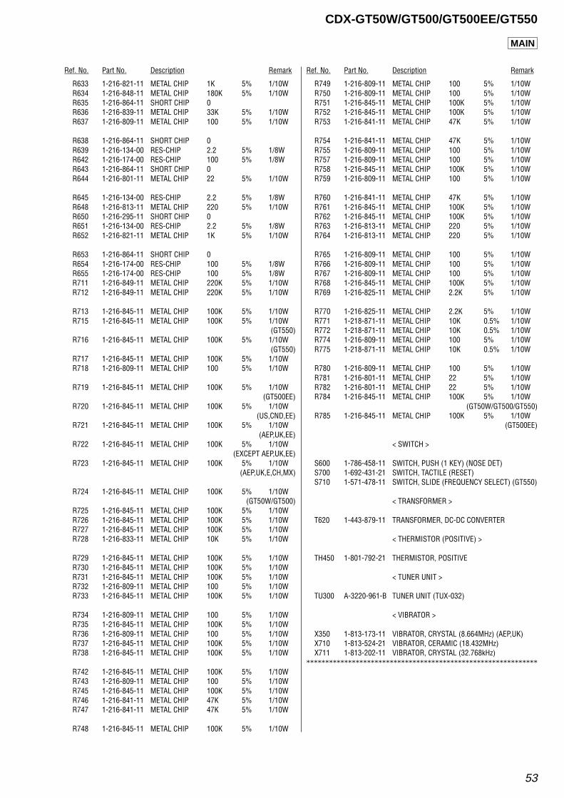
53
CDX-GT50W/GT500/GT500EE/GT550
Ref. No. Part No. Description Remark Ref. No. Part No. Description Remark
R633 1-216-821-11 METAL CHIP 1K 5% 1/10WR634 1-216-848-11 METAL CHIP 180K 5% 1/10WR635 1-216-864-11 SHORT CHIP 0R636 1-216-839-11 METAL CHIP 33K 5% 1/10WR637 1-216-809-11 METAL CHIP 100 5% 1/10W
R638 1-216-864-11 SHORT CHIP 0R639 1-216-134-00 RES-CHIP 2.2 5% 1/8WR642 1-216-174-00 RES-CHIP 100 5% 1/8WR643 1-216-864-11 SHORT CHIP 0R644 1-216-801-11 METAL CHIP 22 5% 1/10W
R645 1-216-134-00 RES-CHIP 2.2 5% 1/8WR648 1-216-813-11 METAL CHIP 220 5% 1/10WR650 1-216-295-11 SHORT CHIP 0R651 1-216-134-00 RES-CHIP 2.2 5% 1/8WR652 1-216-821-11 METAL CHIP 1K 5% 1/10W
R653 1-216-864-11 SHORT CHIP 0R654 1-216-174-00 RES-CHIP 100 5% 1/8WR655 1-216-174-00 RES-CHIP 100 5% 1/8WR711 1-216-849-11 METAL CHIP 220K 5% 1/10WR712 1-216-849-11 METAL CHIP 220K 5% 1/10W
R713 1-216-845-11 METAL CHIP 100K 5% 1/10WR715 1-216-845-11 METAL CHIP 100K 5% 1/10W
(GT550)R716 1-216-845-11 METAL CHIP 100K 5% 1/10W
(GT550)R717 1-216-845-11 METAL CHIP 100K 5% 1/10WR718 1-216-809-11 METAL CHIP 100 5% 1/10W
R719 1-216-845-11 METAL CHIP 100K 5% 1/10W(GT500EE)
R720 1-216-845-11 METAL CHIP 100K 5% 1/10W(US,CND,EE)
R721 1-216-845-11 METAL CHIP 100K 5% 1/10W(AEP,UK,EE)
R722 1-216-845-11 METAL CHIP 100K 5% 1/10W(EXCEPT AEP,UK,EE)
R723 1-216-845-11 METAL CHIP 100K 5% 1/10W(AEP,UK,E,CH,MX)
R724 1-216-845-11 METAL CHIP 100K 5% 1/10W(GT50W/GT500)
R725 1-216-845-11 METAL CHIP 100K 5% 1/10WR726 1-216-845-11 METAL CHIP 100K 5% 1/10WR727 1-216-845-11 METAL CHIP 100K 5% 1/10WR728 1-216-833-11 METAL CHIP 10K 5% 1/10W
R729 1-216-845-11 METAL CHIP 100K 5% 1/10WR730 1-216-845-11 METAL CHIP 100K 5% 1/10WR731 1-216-845-11 METAL CHIP 100K 5% 1/10WR732 1-216-809-11 METAL CHIP 100 5% 1/10WR733 1-216-845-11 METAL CHIP 100K 5% 1/10W
R734 1-216-809-11 METAL CHIP 100 5% 1/10WR735 1-216-845-11 METAL CHIP 100K 5% 1/10WR736 1-216-809-11 METAL CHIP 100 5% 1/10WR737 1-216-845-11 METAL CHIP 100K 5% 1/10WR738 1-216-845-11 METAL CHIP 100K 5% 1/10W
R742 1-216-845-11 METAL CHIP 100K 5% 1/10WR743 1-216-809-11 METAL CHIP 100 5% 1/10WR745 1-216-845-11 METAL CHIP 100K 5% 1/10WR746 1-216-841-11 METAL CHIP 47K 5% 1/10WR747 1-216-841-11 METAL CHIP 47K 5% 1/10W
R748 1-216-845-11 METAL CHIP 100K 5% 1/10W
R749 1-216-809-11 METAL CHIP 100 5% 1/10WR750 1-216-809-11 METAL CHIP 100 5% 1/10WR751 1-216-845-11 METAL CHIP 100K 5% 1/10WR752 1-216-845-11 METAL CHIP 100K 5% 1/10WR753 1-216-841-11 METAL CHIP 47K 5% 1/10W
R754 1-216-841-11 METAL CHIP 47K 5% 1/10WR755 1-216-809-11 METAL CHIP 100 5% 1/10WR757 1-216-809-11 METAL CHIP 100 5% 1/10WR758 1-216-845-11 METAL CHIP 100K 5% 1/10WR759 1-216-809-11 METAL CHIP 100 5% 1/10W
R760 1-216-841-11 METAL CHIP 47K 5% 1/10WR761 1-216-845-11 METAL CHIP 100K 5% 1/10WR762 1-216-845-11 METAL CHIP 100K 5% 1/10WR763 1-216-813-11 METAL CHIP 220 5% 1/10WR764 1-216-813-11 METAL CHIP 220 5% 1/10W
R765 1-216-809-11 METAL CHIP 100 5% 1/10WR766 1-216-809-11 METAL CHIP 100 5% 1/10WR767 1-216-809-11 METAL CHIP 100 5% 1/10WR768 1-216-845-11 METAL CHIP 100K 5% 1/10WR769 1-216-825-11 METAL CHIP 2.2K 5% 1/10W
R770 1-216-825-11 METAL CHIP 2.2K 5% 1/10WR771 1-218-871-11 METAL CHIP 10K 0.5% 1/10WR772 1-218-871-11 METAL CHIP 10K 0.5% 1/10WR774 1-216-809-11 METAL CHIP 100 5% 1/10WR775 1-218-871-11 METAL CHIP 10K 0.5% 1/10W
R780 1-216-809-11 METAL CHIP 100 5% 1/10WR781 1-216-801-11 METAL CHIP 22 5% 1/10WR782 1-216-801-11 METAL CHIP 22 5% 1/10WR784 1-216-845-11 METAL CHIP 100K 5% 1/10W
(GT50W/GT500/GT550)R785 1-216-845-11 METAL CHIP 100K 5% 1/10W
(GT500EE)
< SWITCH >
S600 1-786-458-11 SWITCH, PUSH (1 KEY) (NOSE DET)S700 1-692-431-21 SWITCH, TACTILE (RESET)S710 1-571-478-11 SWITCH, SLIDE (FREQUENCY SELECT) (GT550)
< TRANSFORMER >
T620 1-443-879-11 TRANSFORMER, DC-DC CONVERTER
< THERMISTOR (POSITIVE) >
TH450 1-801-792-21 THERMISTOR, POSITIVE
< TUNER UNIT >
TU300 A-3220-961-B TUNER UNIT (TUX-032)
< VIBRATOR >
X350 1-813-173-11 VIBRATOR, CRYSTAL (8.664MHz) (AEP,UK)X710 1-813-524-21 VIBRATOR, CERAMIC (18.432MHz)X711 1-813-202-11 VIBRATOR, CRYSTAL (32.768kHz)
*************************************************************
MAIN
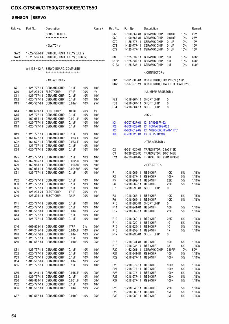
54
CDX-GT50W/GT500/GT500EE/GT550
SENSOR BOARD**************
< SWITCH >
SW2 1-529-566-61 SWITCH, PUSH (1 KEY) (SELF)SW3 1-529-566-61 SWITCH, PUSH (1 KEY) (DISC IN)
*************************************************************
A-1132-412-A SERVO BOARD, COMPLETE**********************
< CAPACITOR >
C7 1-125-777-11 CERAMIC CHIP 0.1uF 10% 10VC10 1-126-208-21 ELECT CHIP 47uF 20% 4VC11 1-125-777-11 CERAMIC CHIP 0.1uF 10% 10VC12 1-125-777-11 CERAMIC CHIP 0.1uF 10% 10VC13 1-100-567-81 CERAMIC CHIP 0.01uF 10% 25V
C14 1-104-609-11 ELECT CHIP 100uF 20% 4VC15 1-125-777-11 CERAMIC CHIP 0.1uF 10% 10VC16 1-162-964-11 CERAMIC CHIP 0.001uF 10% 50VC17 1-125-777-11 CERAMIC CHIP 0.1uF 10% 10VC18 1-125-777-11 CERAMIC CHIP 0.1uF 10% 10V
C19 1-125-777-11 CERAMIC CHIP 0.1uF 10% 10VC20 1-164-677-11 CERAMIC CHIP 0.033uF 10% 16VC22 1-164-677-11 CERAMIC CHIP 0.033uF 10% 16VC23 1-125-777-11 CERAMIC CHIP 0.1uF 10% 10VC24 1-125-777-11 CERAMIC CHIP 0.1uF 10% 10V
C25 1-125-777-11 CERAMIC CHIP 0.1uF 10% 10VC26 1-162-966-11 CERAMIC CHIP 0.0022uF 10% 50VC29 1-162-968-11 CERAMIC CHIP 0.0047uF 10% 50VC30 1-162-968-11 CERAMIC CHIP 0.0047uF 10% 50VC31 1-125-777-11 CERAMIC CHIP 0.1uF 10% 10V
C32 1-125-777-11 CERAMIC CHIP 0.1uF 10% 10VC33 1-125-777-11 CERAMIC CHIP 0.1uF 10% 10VC36 1-125-777-11 CERAMIC CHIP 0.1uF 10% 10VC39 1-126-208-21 ELECT CHIP 47uF 20% 4VC40 1-126-395-11 ELECT CHIP 22uF 20% 16V
C41 1-125-777-11 CERAMIC CHIP 0.1uF 10% 10VC42 1-125-777-11 CERAMIC CHIP 0.1uF 10% 10VC43 1-100-567-81 CERAMIC CHIP 0.01uF 10% 25VC44 1-125-777-11 CERAMIC CHIP 0.1uF 10% 10VC45 1-125-777-11 CERAMIC CHIP 0.1uF 10% 10V
C46 1-162-923-11 CERAMIC CHIP 47PF 5% 50VC47 1-164-245-11 CERAMIC CHIP 0.015uF 10% 25VC48 1-100-567-81 CERAMIC CHIP 0.01uF 10% 25VC49 1-125-777-11 CERAMIC CHIP 0.1uF 10% 10VC50 1-100-567-81 CERAMIC CHIP 0.01uF 10% 25V
C51 1-125-777-11 CERAMIC CHIP 0.1uF 10% 10VC52 1-125-777-11 CERAMIC CHIP 0.1uF 10% 10VC53 1-125-777-11 CERAMIC CHIP 0.1uF 10% 10VC54 1-100-567-81 CERAMIC CHIP 0.01uF 10% 25VC55 1-125-777-11 CERAMIC CHIP 0.1uF 10% 10V
C56 1-164-245-11 CERAMIC CHIP 0.015uF 10% 25VC58 1-125-777-11 CERAMIC CHIP 0.1uF 10% 10VC60 1-162-964-11 CERAMIC CHIP 0.001uF 10% 50VC62 1-125-777-11 CERAMIC CHIP 0.1uF 10% 10VC66 1-100-567-81 CERAMIC CHIP 0.01uF 10% 25V
C67 1-100-567-81 CERAMIC CHIP 0.01uF 10% 25V
C68 1-100-567-81 CERAMIC CHIP 0.01uF 10% 25VC69 1-100-567-81 CERAMIC CHIP 0.01uF 10% 25VC70 1-125-777-11 CERAMIC CHIP 0.1uF 10% 10VC71 1-125-777-11 CERAMIC CHIP 0.1uF 10% 10VC72 1-125-777-11 CERAMIC CHIP 0.1uF 10% 10V
C80 1-125-837-11 CERAMIC CHIP 1uF 10% 6.3VC132 1-125-837-11 CERAMIC CHIP 1uF 10% 6.3VC133 1-125-837-11 CERAMIC CHIP 1uF 10% 6.3V
< CONNECTOR >
CN1 1-691-380-61 CONNECTOR, FFC/FPC (ZIF) 16PCN2 1-817-275-21 CONNECTOR, BOARD TO BOARD 28P
< JUMPER RESISTOR >
FB2 1-216-864-11 SHORT CHIP 0FB3 1-216-864-11 SHORT CHIP 0FB4 1-216-864-11 SHORT CHIP 0
< IC >
IC1 6-707-327-01 IC BA5968FP-E2IC2 6-708-729-01 IC TC94A70FG-002IC3 6-806-019-02 IC MB90486BPFV-G-177E1IC6 6-708-728-01 IC BH15LB1WG
< TRANSISTOR >
Q2 6-551-120-01 TRANSISTOR 2SA2119KQ3 8-729-928-90 TRANSISTOR DTC114EEQ21 8-729-904-87 TRANSISTOR 2SB1197K-R
< RESISTOR >
R1 1-218-965-11 RES-CHIP 10K 5% 1/16WR2 1-218-977-11 RES-CHIP 100K 5% 1/16WR5 1-218-969-11 RES-CHIP 22K 5% 1/16WR6 1-218-969-11 RES-CHIP 22K 5% 1/16WR7 1-218-990-81 SHORT CHIP 0
R8 1-218-965-11 RES-CHIP 10K 5% 1/16WR9 1-218-965-11 RES-CHIP 10K 5% 1/16WR10 1-218-990-81 SHORT CHIP 0R11 1-218-941-81 RES-CHIP 100 5% 1/16WR12 1-218-969-11 RES-CHIP 22K 5% 1/16W
R13 1-218-969-11 RES-CHIP 22K 5% 1/16WR14 1-218-929-11 RES-CHIP 10 5% 1/16WR15 1-218-929-11 RES-CHIP 10 5% 1/16WR16 1-218-953-11 RES-CHIP 1K 5% 1/16WR17 1-218-990-81 SHORT CHIP 0
R18 1-218-941-81 RES-CHIP 100 5% 1/16WR19 1-218-935-11 RES-CHIP 33 5% 1/16WR20 1-162-961-11 CERAMIC CHIP 330PF 10% 50VR21 1-218-941-81 RES-CHIP 100 5% 1/16WR22 1-218-977-11 RES-CHIP 100K 5% 1/16W
R23 1-218-977-11 RES-CHIP 100K 5% 1/16WR24 1-218-977-11 RES-CHIP 100K 5% 1/16WR25 1-218-977-11 RES-CHIP 100K 5% 1/16WR26 1-218-977-11 RES-CHIP 100K 5% 1/16WR27 1-218-977-11 RES-CHIP 100K 5% 1/16W
R28 1-218-945-11 RES-CHIP 220 5% 1/16WR29 1-218-989-11 RES-CHIP 1M 5% 1/16WR30 1-218-989-11 RES-CHIP 1M 5% 1/16W
Ref. No. Part No. Description Remark Ref. No. Part No. Description Remark
SENSOR SERVO
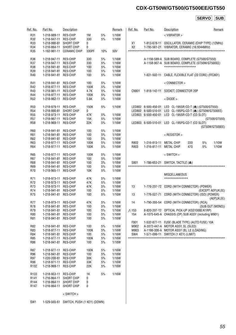
55
CDX-GT50W/GT500/GT500EE/GT550
SERVO SUB
Ref. No. Part No. Description Remark Ref. No. Part No. Description Remark
R31 1-218-989-11 RES-CHIP 1M 5% 1/16WR32 1-218-947-11 RES-CHIP 330 5% 1/16WR33 1-218-990-81 SHORT CHIP 0R34 1-216-864-11 SHORT CHIP 0R35 1-162-961-11 CERAMIC CHIP 330PF 10% 50V
R36 1-218-947-11 RES-CHIP 330 5% 1/16WR37 1-218-947-11 RES-CHIP 330 5% 1/16WR38 1-218-941-81 RES-CHIP 100 5% 1/16WR39 1-218-941-81 RES-CHIP 100 5% 1/16WR40 1-218-941-81 RES-CHIP 100 5% 1/16W
R41 1-218-941-81 RES-CHIP 100 5% 1/16WR42 1-218-977-11 RES-CHIP 100K 5% 1/16WR43 1-218-961-11 RES-CHIP 4.7K 5% 1/16WR44 1-218-977-11 RES-CHIP 100K 5% 1/16WR52 1-218-962-11 RES-CHIP 5.6K 5% 1/16W
R53 1-218-979-11 RES-CHIP 150K 5% 1/16WR54 1-218-990-81 SHORT CHIP 0R55 1-218-973-11 RES-CHIP 47K 5% 1/16WR57 1-218-967-11 RES-CHIP 15K 5% 1/16WR58 1-218-969-11 RES-CHIP 22K 5% 1/16W
R60 1-218-941-81 RES-CHIP 100 5% 1/16WR61 1-218-941-81 RES-CHIP 100 5% 1/16WR62 1-218-941-81 RES-CHIP 100 5% 1/16WR63 1-218-977-11 RES-CHIP 100K 5% 1/16WR64 1-218-977-11 RES-CHIP 100K 5% 1/16W
R65 1-218-977-11 RES-CHIP 100K 5% 1/16WR67 1-218-941-81 RES-CHIP 100 5% 1/16WR68 1-218-941-81 RES-CHIP 100 5% 1/16WR69 1-218-941-81 RES-CHIP 100 5% 1/16WR70 1-218-965-11 RES-CHIP 10K 5% 1/16W
R71 1-218-973-11 RES-CHIP 47K 5% 1/16WR72 1-218-973-11 RES-CHIP 47K 5% 1/16WR73 1-218-973-11 RES-CHIP 47K 5% 1/16WR74 1-218-941-81 RES-CHIP 100 5% 1/16WR75 1-218-941-81 RES-CHIP 100 5% 1/16W
R77 1-218-973-11 RES-CHIP 47K 5% 1/16WR78 1-218-941-81 RES-CHIP 100 5% 1/16WR79 1-218-941-81 RES-CHIP 100 5% 1/16WR80 1-218-941-81 RES-CHIP 100 5% 1/16WR81 1-218-941-81 RES-CHIP 100 5% 1/16W
R82 1-218-941-81 RES-CHIP 100 5% 1/16WR83 1-218-977-11 RES-CHIP 100K 5% 1/16WR84 1-218-941-81 RES-CHIP 100 5% 1/16WR85 1-218-977-11 RES-CHIP 100K 5% 1/16WR86 1-218-941-81 RES-CHIP 100 5% 1/16W
R87 1-218-977-11 RES-CHIP 100K 5% 1/16WR96 1-218-941-81 RES-CHIP 100 5% 1/16WR97 1-220-200-81 RES-CHIP 30K 5% 1/16WR98 1-218-971-11 RES-CHIP 33K 5% 1/16WR132 1-218-969-11 RES-CHIP 22K 5% 1/16W
R133 1-218-953-11 RES-CHIP 1K 5% 1/16WR141 1-216-864-11 SHORT CHIP 0R144 1-216-864-11 SHORT CHIP 0R147 1-216-864-11 SHORT CHIP 0
< SWITCH >
SW1 1-529-565-61 SWITCH, PUSH (1 KEY) (DOWN)
< VIBRATOR >
X1 1-813-678-11 OSCILLATOR, CERAMIC (CHIP TYPE) (12MHz)X2 1-795-561-21 VIBRATOR, CERAMIC (16.9344MHz)
*************************************************************
A-1156-589-A SUB BOARD, COMPLETE (GT500/GT550)A-1158-907-A SUB BOARD, COMPLETE (GT50W/GT500EE)
********************
1-831-502-11 CABLE, FLEXIBLE FLAT (22 CORE) (FFC801)
< CONNECTOR >
CN801 1-818-142-11 SOCKET, CONNECTOR 20P
< DIODE >
LED802 6-500-450-01 LED CL-195SR-CD-T (Z) (GT500/GT550)LED802 6-500-510-01 LED CL-195PG-CD-T (Z) (GT50W/GT500EE)LED803 6-500-450-01 LED CL-195SR-CD-T (CD SLOT)
(GT500/GT550)LED803 6-500-510-01 LED CL-195PG-CD-T (CD SLOT)
(GT50W/GT500EE)
< RESISTOR >
R802 1-216-813-11 METAL CHIP 220 5% 1/10WR803 1-216-817-11 METAL CHIP 470 5% 1/10W
< SWITCH >
S801 1-786-653-21 SWITCH, TACTILE (Z)*************************************************************
MISCELLANEOUS***************
13 1-776-207-72 CORD (WITH CONNECTOR) (POWER)(EXCEPT AEP,UK,EE)
13 1-776-527-71 CORD (WITH CONNECTOR) (ISO) (POWER)(AEP,UK,EE)
14 1-790-355-54 CORD (WITH CONNECTOR) (RCA)(SUB OUT (MONO))
0153 8-820-207-12 OPTICAL PICK-UP (KSS1000E/K1RP)154 A-1075-645-A CHASSIS (OP) SUB ASSY (including M901)
F901 1-532-877-11 FUSE (BLADE TYPE) (AUTO FUSE) 10AM902 A-3372-447-A MOTOR ASSY, SL (SLED)M903 A-1166-300-A MOTOR ASSY (B), LE (LOADING)SW4 1-571-099-11 SWITCH (1 KEY) (LIMIT)
*************************************************************
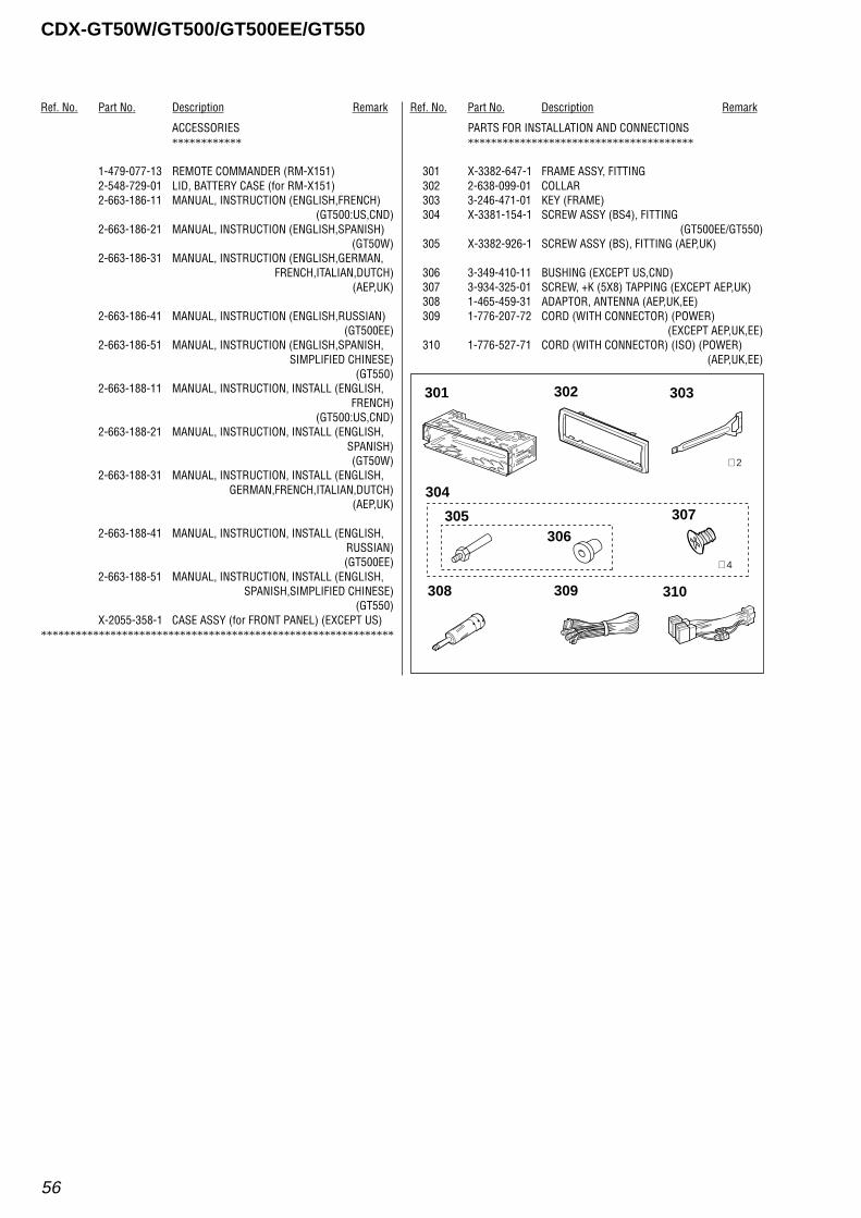
56
CDX-GT50W/GT500/GT500EE/GT550
Ref. No. Part No. Description Remark Ref. No. Part No. Description Remark
ACCESSORIES************
1-479-077-13 REMOTE COMMANDER (RM-X151)2-548-729-01 LID, BATTERY CASE (for RM-X151)2-663-186-11 MANUAL, INSTRUCTION (ENGLISH,FRENCH)
(GT500:US,CND)2-663-186-21 MANUAL, INSTRUCTION (ENGLISH,SPANISH)
(GT50W)2-663-186-31 MANUAL, INSTRUCTION (ENGLISH,GERMAN,
FRENCH,ITALIAN,DUTCH)(AEP,UK)
2-663-186-41 MANUAL, INSTRUCTION (ENGLISH,RUSSIAN)(GT500EE)
2-663-186-51 MANUAL, INSTRUCTION (ENGLISH,SPANISH,SIMPLIFIED CHINESE)
(GT550)2-663-188-11 MANUAL, INSTRUCTION, INSTALL (ENGLISH,
FRENCH)(GT500:US,CND)
2-663-188-21 MANUAL, INSTRUCTION, INSTALL (ENGLISH,SPANISH)(GT50W)
2-663-188-31 MANUAL, INSTRUCTION, INSTALL (ENGLISH,GERMAN,FRENCH,ITALIAN,DUTCH)
(AEP,UK)
2-663-188-41 MANUAL, INSTRUCTION, INSTALL (ENGLISH,RUSSIAN)(GT500EE)
2-663-188-51 MANUAL, INSTRUCTION, INSTALL (ENGLISH,SPANISH,SIMPLIFIED CHINESE)
(GT550)X-2055-358-1 CASE ASSY (for FRONT PANEL) (EXCEPT US)
*************************************************************
PARTS FOR INSTALLATION AND CONNECTIONS***************************************
301 X-3382-647-1 FRAME ASSY, FITTING302 2-638-099-01 COLLAR303 3-246-471-01 KEY (FRAME)304 X-3381-154-1 SCREW ASSY (BS4), FITTING
(GT500EE/GT550)305 X-3382-926-1 SCREW ASSY (BS), FITTING (AEP,UK)
306 3-349-410-11 BUSHING (EXCEPT US,CND)307 3-934-325-01 SCREW, +K (5X8) TAPPING (EXCEPT AEP,UK)308 1-465-459-31 ADAPTOR, ANTENNA (AEP,UK,EE)309 1-776-207-72 CORD (WITH CONNECTOR) (POWER)
(EXCEPT AEP,UK,EE)310 1-776-527-71 CORD (WITH CONNECTOR) (ISO) (POWER)
(AEP,UK,EE)
301
304
302
305306
309 310
303
× 2
× 4
308
307

57
CDX-GT50W/GT500/GT500EE/GT550
MEMO

58
CDX-GT50W/GT500/GT500EE/GT550
REVISION HISTORY
Clicking the version allows you to jump to the revised page.Also, clicking the version at the upper on the revised page allows you to jump to the next revised page.
Ver. Date Description of Revision1.0 2005. 12 New