sony ctv25 ba-4 training manual - audio | video | circuits
TRANSCRIPT

S® Training Manual
Circuit Description and Troubleshooting
Course: CTV-25 R1
ColorTelevisionBA-4 Chassis
Table of ContentsIntroduction
The Trinitron ® Picture Tube 1
The Trinitron Electron Gun Operation 1
The Trinitron Screen 7
Picture Tube Defect Symptoms 9
Picture Tube Handling and VacuumDisposal 13
Overall Block Diagram 15
Power Supply 15
Communications 15
Video Processing 15
Deflection 15
Power Supply - 20” TV & Smaller 17
The Converter Stage 17
The Voltage Output Stage 17
The Power Output Control 17
Converter 19
The Rectifier 19
The Oscillator 19
Converter Voltage Outputs 29
B+ Regulation - 13” & 20” TV 33
Regulation 33
Additional Circuits 33
Power Supply Block - 27” Models 37
Standby Power Supply 39
Basic Oscillator 39
Additional Components 41
B+ Regulation - 27” TV 45
Regulation 45
Soft Start Circuit 45
Power On/Communications Block 47
Degaussing Circuitry 49
Concept 49
Circuit Operation 49
Power ON 53
Communications 57
Start 57
Run 57
Video Processing Block 61
Tuner 61
Video Inputs 61
Digital Comb Filter 61
Video Output 63

TV Reception 65
Reception from Power ON 65
Channel Change Audio Mute 65
Auto Station Programming 65
Video Inputs 69
Video Output 73
Spot Elimination Circuit 75
Troubleshootintg 77
Video Block - 27” With PIP 79
Picture in Picture (PIP) Board Signal Flow 79
Picture in Picture Processing 81
Deflection Block 83
Vertical Deflection 85
Horizontal Deflection 89
Protection 93
Troubleshooting 95
Self Diagnostic 99
Timer / Standby Light 99
Self-Diagnostic On Screen Display 99
Self-Diagnostic Circuit 101

Introduction
Sony TV Models Covered by this ManualBA-4 Chassis – Current Models Covered
KV13M40 KV20M40 KV27S40 KV27V40
KV13M50 KV20M40 KV27S45 KV27V45
KV13M51 KV20S40 KV27S65 KV27V65
KV20S41
KV20V80
PurposeThe purpose of this book is to:
• Show through diagrams and explanation how the Sony Trinitron Picture tube now works because it has evolved since inception in1968.
• Provide organized, simplified diagrams that provide an insight to understanding the necessities of the circuit’s operation. This is anessential aid to rapidly determining the cause of a failure.
• Explain the circuit operation and provide tips for troubleshooting where needed. Some parts of the circuit are used only under certainconditions of operation. It is important to know when these additional parts affect the main circuit during operation and how they affectthe main circuits if they are defective.
• Provide some voltages from a working production run set that are not supplied in the service manual. These can be compared to thenon-working unit you are repairing to determine where the fault is.
• Explain the new self diagnostic circuit:
1. How to access it
2. How it works,
3. When to use it
4. The circuits that support it
Note:This note is common to all schematics and block diagrams.All capacitors are uf unless otherwise noted.All resistors are ohms unless otherwise noted.All voltages are dc unless otherwise noted.

1
The Trinitron Picture Tube
The Cathode Ray Tube (CRT) has been slowly changing since its con-ception about 50 years ago. Since then the emitter, accelerator andfocus structures at the “gun” end have been added to the vacuum tubeto shape and control the amount of electrons from the gun.
At the target end of the CRT, the luminescent screen is made of a phos-phor mixture. Phosphor glows white when struck by electrons. Phos-phor brightness is directly proportional to the amount of electrons thatstrike the phosphor. The CRT sport brightness was controllable with agun and phosphor screen.
The electron beam produced a spot of light that was stationary on thephosphor screen. Placing an electromagnetic field near the electronbeam after it left the gun created movement. The spot intensity andlocation were now controllable and the CRT became known as the pic-ture tube.
To produce a color picture on the CRT screen; three independent gunstructures are used. The electron guns produce different amounts ofelectrons targeted to their corresponding Red, Green and Blue phos-phors. Red, Green and Blue are the primary colors for light.
In 1968 the Sony Trinitron picture tube was a departure from the tradi-tional three-gun color picture tube. Three major changes to the old colortube created a distinctive Trinitron picture tube:
1. Instead of three small electron guns, focus was improved using onelarge electron gun structure that all three beams pass through.
2. Electrostatic convergence plates were added to bend the outer elec-tron beams so they would land on the corresponding red and bluecolor phosphor.
3. A continuous vertical slotted aperture grill at the screen end that:• Reduces the effects of terrestrial magnetism.• Prevents adjacent and stray electrons from striking the wrong phos-
phor.• Allows more electrons to pass, increasing brightness without short-
ening life.• Results in a flat screen. This reduces annoying room light reflections
(glare).
The remainder of this document is divided into four sections explainingthe construction of Trinitron tube as an aid to the service technician:
• The Trinitron Electron Gun Operation• The Trinitron Screen• Picture Tube Defect Symptoms• Picture Tube Handling and Vacuum Disposal
The Trinitron Electron Gun OperationThe Sony Trinitron electron gun consists of three cathode assemblies,five grid structures and convergence plates:
Three cathode assembliesWhen heated, electrons are given off from a Barium Carbonate (BaCO
3)
surface deposited onto a cap. The cap serves as a holder for the BaCO3,
white mixture. The cap is fastened to a sleeve that houses a heatingelement (filament). This assembly is called a cathode.
There are three cathodes in the beginning part of the gun assembly bythe pins of the CRT. They all supply electrons in controlled amounts.The center cathode on the Trinitron tube produces the amount of elec-trons that correspond to the green color information. These electronswill eventually land on the green phosphor if things go well on the jour-ney. The outer cathodes are angled slightly to send electrons throughthe gun structure. Their final targets are the red and blue phosphor atthe screen.
Next a voltage is connected to the cathode (sleeve) and a more positivevoltage to the second grid (two) in the gun structure. This difference inpotential will pull the electrons from the cathode’s Barium Carbonate(BaCO
3) surface into the gun structure. The difference in potential volt-
age between the cathode and grid two will determine the amount of elec-trons emitted. More electrons landing on the phosphor (screen) will in-crease the color spot intensity.

2

3
Five Grid StructuresThe electron gun consists of the cathode and several metal rings calledgrids. The grid name came from the controlling grids in a vacuum tubewhere the interelectrode elements were originally shaped like a screenmesh. There is no structural resemblance between the picture andvacuum tube grids. In the picture tube, the grid rings are applied differ-ent electrical potentials to focus (shape) and accelerate (speed) the elec-trons from the cathodes. Each part of the gun has a voltage applied to itfor a specific purpose.
Trinitron Electron Gun PartsName Purpose Applied Voltage
Filament / Heater(Inside the cathodeassembly).
Brings the cathode toemission temperature.
Test voltage = 6 Vdc @0.64 Amp. Actual voltage= FBT pulse, 6V rms.
Cathode assembly Houses the electronemitting chemical and theheater.
R, G or B signal voltage.+200V= Cutoff. Noelectrons output.0V = All electrons output.
Grid 1 / Control Grid Reference potential forcathode emission.
Ground via currentlimiting resistor.
Grid 2 / Screen Grid Brightness limit. 400Vdc (approx.)Grid 3 / Accelerating Accelerate stream. HV from FBT*.Grid 4 / Focus Sets focus point. 300Vdc (approx.)
Focus Control range= 200Vdc to 1kVdc.
Grid 5 / Accelerating Post Accelerating. HV from FBT*.*FBT = Flyback Transformer in consumer TVs. Transformer is assembled withrectifiers in a doubler or tripler configuration to develop 25-35kV of DC. The highvoltage is used in the picture tube to accelerate electrons. Larger picture tubesrequire a higher high voltage from the FBT to move the electrons a longer distance.
Control Grid One
Electrons at the cathode are attracted to a positive potential. The gridone ring is the next electrode structure in the electron gun. In consumerTVs, grid one is fixed at a 0Vdc potential for reference. If a positivepotential were placed on the cathode, electrons would not be attractedto grid one. At a +200Vdc potential, electrons would not leave the cath-ode. If no electrons enter the gun, the TV screen is dark. The picturetube is said to be in “cutoff”.
On the other hand, placing the cathode at the same potential as grid one(0Vdc) is the same as if grid one were invisible. The maximum amount ofelectrons is attracted toward the positive grid two structure, resulting inmaximum screen brightness.
By varying the voltage at the cathode from 0 Vdc to +200Vdc (cutoff), theamount of electrons available to the gun structure to produce screenbrightness can be controlled.
Screen Grid Two
The higher voltage at the second grid ring accelerates the electron beam.This voltage is connected to the TV circuitry’s “screen control”. The screencontrol is adjusted to limit the maximum beam acceleration (brightness).This limit avoids over driving the tube which shortens the life of the cath-odes and phosphors.
Acceleration Grid Three
The very highest voltage in a TV (from the flyback transformer) is appliedto the third grid ring. This creates a large magnetic field to further accel-erate the three electron streams from the cathodes.
Focus Grid Four and Acceleration Grid Five
The lower voltage at focus grid ring four slows down the electron streamso they bunch up, thickening the beams. By varying the focus voltageapplied to grid four, the beam thickness is controlled. A thicker beammeans the electron stream will focus at a point closer to the gun (beforethe screen).
When a very bright spot is called for, more electrons are sent from thecathodes. As a result the beam is at its thickest at the G4 focus ring. Ina small electron gun, the G4 focus ring is closer to the thick beam thanthe single Trinitron gun where the focus ring is much larger.
Grid four’s magnetic field is the strongest at the metal grid ring. Moreperipheral electrons are attracted to the focus grid ring of the smallerelectron gun. Some of these peripheral electrons are lost from the streamas G4 grid current, limiting beam thickness. The limited beam thicknessresults in a shift in focus point. This causes reduced focus during bright-ness peaks in the smaller electron gun. Therefore, at high brightnesslevels it is advantageous to have a large G4 focus structure. A widerdynamic focus range is achievable with the large single Trinitron gun.

4
5
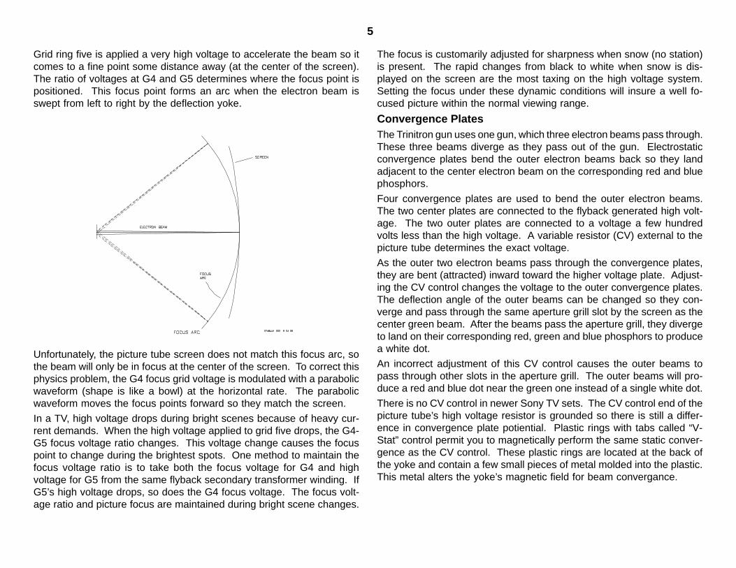
Grid ring five is applied a very high voltage to accelerate the beam so itcomes to a fine point some distance away (at the center of the screen).The ratio of voltages at G4 and G5 determines where the focus point ispositioned. This focus point forms an arc when the electron beam isswept from left to right by the deflection yoke.
Unfortunately, the picture tube screen does not match this focus arc, sothe beam will only be in focus at the center of the screen. To correct thisphysics problem, the G4 focus grid voltage is modulated with a parabolicwaveform (shape is like a bowl) at the horizontal rate. The parabolicwaveform moves the focus points forward so they match the screen.
In a TV, high voltage drops during bright scenes because of heavy cur-rent demands. When the high voltage applied to grid five drops, the G4-G5 focus voltage ratio changes. This voltage change causes the focuspoint to change during the brightest spots. One method to maintain thefocus voltage ratio is to take both the focus voltage for G4 and highvoltage for G5 from the same flyback secondary transformer winding. IfG5’s high voltage drops, so does the G4 focus voltage. The focus volt-age ratio and picture focus are maintained during bright scene changes.
The focus is customarily adjusted for sharpness when snow (no station)is present. The rapid changes from black to white when snow is dis-played on the screen are the most taxing on the high voltage system.Setting the focus under these dynamic conditions will insure a well fo-cused picture within the normal viewing range.
Convergence PlatesThe Trinitron gun uses one gun, which three electron beams pass through.These three beams diverge as they pass out of the gun. Electrostaticconvergence plates bend the outer electron beams back so they landadjacent to the center electron beam on the corresponding red and bluephosphors.
Four convergence plates are used to bend the outer electron beams.The two center plates are connected to the flyback generated high volt-age. The two outer plates are connected to a voltage a few hundredvolts less than the high voltage. A variable resistor (CV) external to thepicture tube determines the exact voltage.
As the outer two electron beams pass through the convergence plates,they are bent (attracted) inward toward the higher voltage plate. Adjust-ing the CV control changes the voltage to the outer convergence plates.The deflection angle of the outer beams can be changed so they con-verge and pass through the same aperture grill slot by the screen as thecenter green beam. After the beams pass the aperture grill, they divergeto land on their corresponding red, green and blue phosphors to producea white dot.
An incorrect adjustment of this CV control causes the outer beams topass through other slots in the aperture grill. The outer beams will pro-duce a red and blue dot near the green one instead of a single white dot.
There is no CV control in newer Sony TV sets. The CV control end of thepicture tube’s high voltage resistor is grounded so there is still a differ-ence in convergence plate potiential. Plastic rings with tabs called “V-Stat” control permit you to magnetically perform the same static conver-gence as the CV control. These plastic rings are located at the back ofthe yoke and contain a few small pieces of metal molded into the plastic.This metal alters the yoke’s magnetic field for beam convergance.

6

7
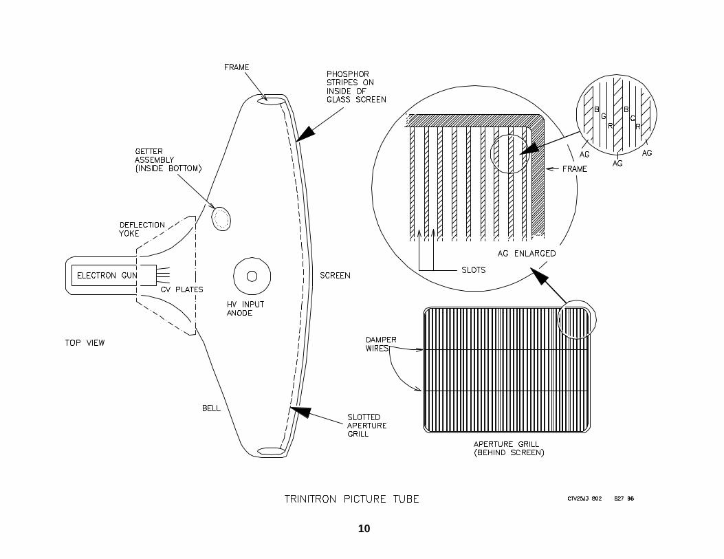
The Trinitron ScreenIn front of the electron gun are the:
• Deflection Yoke• Aperture Grill (AG)• Phosphor Stripes• Getter Assembly
Deflection Yoke
The yoke consists of two coils of wire mounted on the glass bell of thepicture tube in front of the (internal) convergence plates. One coil gener-ates a magnetic field to move the electron beams in the X-axis and theother coil moves the beams in the Y-axis. Guided by the deflection yoke,three electron beams first sweep across the aperture grill along the X-axis from left to right (from the front as you would watch TV). At the endof the horizontal sweep, the beam retraces back to the left side of thescreen. Meanwhile the yoke’s magnetic field moves the three beamsdown (Y-axis) one line before the beams sweep horizontally across theaperture grill again. This process then repeats. Finally, at the bottomright corner of the picture, the beams are returned to the top left corner ofthe screen.
The deflection yoke has difficulty providing a magnetic field to sweep thebeam so it matches the screen shape. The yoke’s magnetic field is stron-ger at the corners of the picture then at the top/bottom and sides (X & Y-axis).
Improvements in deflection yoke construction have compensated for thereduced top/bottom deflection (Y-axis). Along the X-axis, the weakermagnetic field causes the picture to look like an hourglass. This is be-cause there is insufficient picture scan, which produces a dark area atthe left and right sides of the picture tube.
Increasing the current through the horizontal windings of the yoke com-pensates for this hourglass picture. The yoke current is then graduallyincreased line by line until the middle of the picture for maximum width ,the curve is reduced as the beam continues to scan downward. Theresult is a straight picture. This type of yoke distortion to the picture iscalled pincushion distortion. The correction circuit that changes the yokecurrent is called the pincushion stage.
Aperture Grill Construction
The aperture grill (AG) is an aluminum panel located behind the picturetube screen with vertical slits cut out. The aperture grill is welded to asteel frame that holds it completely flat in the vertical direction and curvedin the horizontal direction. Consequently, the resultant picture tube faceshape is like the front of a cylinder. This flatter surface reflects less roomlight and, therefore, produces fewer glares from the ambient light. Thisis another feature that sets the Trinitron apart from other picture tubesthat are spherical in shape.
Although the grill is held flat, it still can move slightly, especially in largertubes. In larger tubes, there are two horizontal wires that run acrossequidistant across the grill, preventing the slots from vibrating or shifting.These two wires found in the grill are called anti-vibration damper wires.
Aperture Grill Purpose
In diagram 5, the slits in the aper-ture grill allow the electron beam topass through and land on the phos-phor. The electron beam meant toland on the green phosphor isshown:

8
9
In diagram 6 you can see the slits have a more important purpose. Whenall three beams are turned ON, the narrow AG slots prevent adjacentelectron beams from landing on the wrong color phosphor. The aperturegrill slots only allow electron beams to pass through and land on theircorresponding color phosphor.
Phosphor Stripes
Phosphor is a powder that becomes luminescent when bombarded byelectrons. The color and persistence of phosphor glow after electronbombardment is determined by using additional chemicals combined withthe phosphor. Three different color phosphors are painted in verticalstrips that correspond to aperture grill slits. The phosphor strips are sepa-rated by carbon stripes that do not glow when struck by electrons. Thesecarbon stripes allow for manufacturing tolerances when making the AGand painting the phosphor stripes.
Getter Assembly
Electron emission efficiency and cathode life are greatly dependent upona clean environment inside the CRT. After the air is pumped out of theCRT and sealed, residual water vapor, carbon dioxide and oxygen inevi-tably remain.
A small cup attached to the gun assembly containing a barium com-pound is placed inside the picture tube. After sealing the glass picturetube, the Getter is ”flashed” with a high level of RF energy. The bariumcompound heats up and evaporates, combining with the residual unde-sirable elements in the picture. The resultant compounds that are cre-ated coat the inside walls of the picture tube without consequence. The
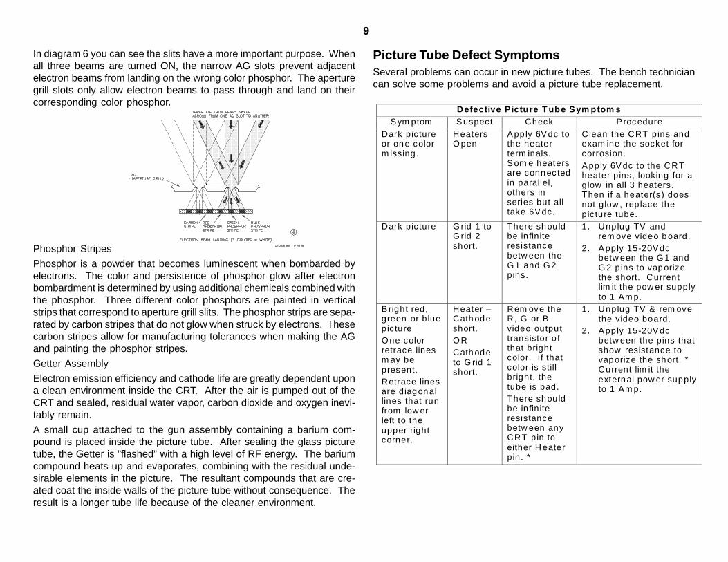
Picture Tube Defect SymptomsSeveral problems can occur in new picture tubes. The bench techniciancan solve some problems and avoid a picture tube replacement.
result is a longer tube life because of the cleaner environment.
Defective P ictu re T ube S ym ptom sS ym ptom S uspect Check P rocedure
Dark pic tureor one colorm issing.
HeatersO pen
A pply 6V dc tothe heaterterm inals.S om e heatersare connec tedin parallel,others inseries but alltake 6V dc.
C lean the CRT pins andexam ine the socket forcorrosion.A pply 6V dc to the CRTheater pins, looking for aglow in all 3 heaters.Then if a heater(s ) doesnot glow , rep lace thepic ture tube.
Dark pic ture G rid 1 toG rid 2short.
There shouldbe in fin iteresistancebetw een theG 1 and G 2pins.
1. Unplug TV andrem ove video board.
2. A pply 15-20V dcbetw een the G 1 andG 2 p ins to vaporizethe short. Currentlim it the pow er supplyto 1 Am p.
B right red,green or bluepic tureO ne colorretrace linesm ay bepresent.Retrace linesare diagonallines that runfrom low erleft to theupper rightcorner.
Heater –Cath odeshort.O RCath odeto G rid 1short.
Rem ove theR, G or Bvideo outputtransistor o fthat brightcolor. If thatcolor is stillbright, thetube is bad.There shouldbe in fin iteresistancebetw een anyCRT pin toeither H eaterpin. *
1. Unplug TV & rem ovethe video board.
2. A pply 15-20V dcbetw een the pins thatshow resistance tovaporize the short. *Current lim it theexternal pow er supplyto 1 Am p.
10

11
D e fe c t iv e P ic tu r e T u b e S y m p to m sS y m p t o m S u s p e c t C h e c k P ro c e d u r e
B r ig h t p ic t u rew it h r e t r a c el in e s a n d / o rp o o r f o c u s .
G r id 2 t oh ig hv o l t a g eG r id 3le a k a g e .
S y m p t o m ist h a t a l l t h re ec o lo r s a r eb r ig h t .
R e d u c e G 2 / s c re e nv o l t a g e t o t h e lo w e s ts e t t in g .V a ry f o c u s c o n t ro l t o b o t hl im it s s e v e r a l t im e s .P u t o n s a f e t y a p p a r e l .P la c e t h e t u b e fa c e d o w na n d l ig h t ly t a p th e n e c k t od is lo d g e t h e p a r t ic le .
B la c k s p o t o nt h e s c re e n .( s e e b l a c ks p o td ia g r a m )
D u s tlo d g e d int h ea p e r t u r eg r i l l .
G e n e r a t e aw h it e r a s t e r .I n s p e c t g r i l lw it hm a g n i fy in gg la s s .
M a rk lo c a t i o n a n d p u l lT V . F o l lo w s a f e t yin s t ru c t io n s .A p p ly lig h t im p a c t w it hru b b e r m a l le t ( s e ed ia g r a m ) .
R G BR a in b o w .( s e e r a in b o wp ic t u re )
A p e r t u r eg r i l l w a su n s e a t e din t r a n s i t .
R a in b o w o fc o lo r s c a ns t a r t a t t h et o p o r b o t t o m(b o t t o mra in b o ws h o w n ) .
A lo o s e a p e r t u re g r i l l isd a n g e r o u s a n d m a yc a u s e t u b e im p lo s io n .U s e a l l s a f e t yp re c a u t i o n s . D o n o t ja rs e t . T ra n s p o r t f a c ed o w n , .
P u r i t y / B e a mla n d in g is o f f .
T h e T V ’sd e g a u s s in g c i rc u itd id n o td e m a g n et iz ea p e r t u r eg r i l l m e t a ls u p p o r t .
S a m e c o lo rb lo t c h e sre m a in a t t h a ta r e a o f t h es c re e nre g a rd l e s s o fp ic t u re s c re e nc h a n g e s .
D o n o t m a n u a l lyD e g a u s s t h e p ic tu r etu b e w i t h y o u r s t r o n gd e g a u s s in g c o i l * * .R e p a ir t h e T V ’sd e g a u s s in g c i rc u i t . T h et h e rm is t o r is u s u a l ly a tfa u l t .
* O n ly th e h e ater p in s sh ou ld h av e res is tan c e. A ll oth er p in s h av ein fin ite (∞ ) res is tan c e to e ac h oth er an d to eith er h e ater p in s .H ig h ly -u sed p ic tu re tu b es th at h av e a h e ater -c ath od e le ak ag e/sh orth av e a low res to rat ion su c c ess lev el.** D o n ot m an u ally D eg au ss. N ew 2 7 ’ – 3 5 ” p ic tu re tu b es arem ag n etic ally “c on d it ion ed ” for op t im um b eam lan d in g . S tron g m an uad eg au s s in g w ill d es troy th is c on d it ion in g . A p p ly in g disc m ag n ets (P /N= 1 -4 5 2 -0 9 4 -0 0 ) to th e b ell of th e p ic tu re tu b e is th e on ly w ay toc om p en sate fo r los t m ag n etic c on d it ion in g . T h e S on y m an u ald eg au s s in g tool c an b e u s ed to d eg au ss th es e tu b es b ec au s e of th ered u c ed fie ld in ten s ity (P /N = 7 -7 0 0 -7 8 1 -0 1 ).

12

13
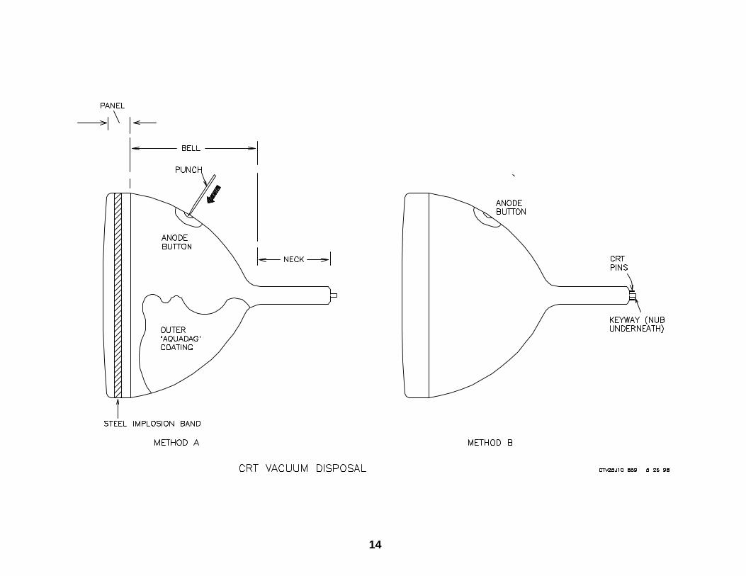
Picture Tube Handling and Vacuum DisposalOnce you have determined that the CRT is inoperative, air should be letinto the tube. This will reduce the risk of implosion caused by a suddenloss of vacuum.
There are two good methods of “airing” the tube:
A. Puncture through the anode button.B. Break the thin glass seal at the neck.The first method allows air to enter the tube gradually.
A. Puncture through the anode button.Air can be let in gradually by making a hole inside the high voltage an-ode. The anode is located at the stronger bell part of the picture tube.Read the procedure below first:1. Put on protective goggles, gloves, apron and shoes as specified in
the picture tube safety precautions.2. Check that there is still a steel implosion protection band about the
panel of the 27” or larger picture tubes. See the picture for the loca-tion. If it is not present, do not air the tube. Call for professionaldisposal.
3. Next, the high voltage stored by the picture tube must be discharged.The picture tube capacitor has two plates. One plate is inside, con-nected to the HV anode button. The other plate is outside, con-nected to ground. The tube’s outside conductive plate is a blackgraphite “aquadag” coating. Use a high voltage probe (selfcontained)to gradually discharge the high voltage (HV) with the TVoff.
4. Clip one end of a jumper wire to the chassis strap resting on theconductive black aquadag coating of the picture tube bell. Connectthe other end of the jumper wire to the anode terminal. Leave thejumper there for about a minute to make sure the picture tube capaci-tor is completely discharged. During this time, inspect the bottomarea of the picture tube to make sure the ground strap is touching theblack aquadag coating.
5. Using a small screwdriver or center punch as a puncturing tool, seatit into the center of the soft lead anode button cavity (hole). Thepuncturing tool must be able to pass through the anode hole and nottouch the anode button’s outer metal rim.
6. Being careful not to hit the glass with the hammer, gently tap the toolfurther into the anode button. The anode is made of a soft leadamalgam that will give inward.
7. The hissing sound when the punch is wiggled out means that thetube is “aired”.
B. Break the thin glass seal at the neck.Method B for releasing the picture tube vacuum is to break the glass nubat the neck of the tube. Read the procedure below first:1. Put on protective goggles, gloves, apron and shoes as specified in
the picture tube safety precautions.2. Check that there is still a metal implosion protection band about the
panel of the 27” or larger picture tubes. If the band has been re-moved, do not proceed with this vacuum disposal procedure.
3. There is a plastic keyway at the pins of the CRT. Remove the plastickeyway by wiggling it off. This exposes the glass nub that was sealedto maintain the vacuum.
4. With a pair of long nose pliers or diagonal cutters, break this glassnub by squeezing it to shatter the glass. The tube is “aired”.
Picture Tube Safety Precautions• Wear safety goggles even over glasses to prevent side
glass entry
• Handle the picture tube with the correct size work glovesfor your hands to avoid slipping
• Change to a thick long sleeve shirt to avoid exposing yourskin to glass fragments
• Wear a thick rubber apron
• Wear shoes to protect your feet
• Find a partner to help move or reposition the picture tube.Your partner needs protective gear more than you do
14

15
Overall Block Diagram
A TV set consists of several stages or blocks:
• Power Supply
• Power On/Communications
• Video Processing
• Deflection
Each stage has a purpose and is activated in sequence to properly powerup the set.
Power SupplyThe purpose of the power supply is to convert the incoming 120Volts ACto some of the DC voltages required to operate the set, the most impor-tant of which is the Standby +5Vdc. Standby +5Vdc is present when theset is plugged in and is used to power the Micro so it can respond to a TVpower ON command from the user.
Power On/CommunicationsThree things occur when the power button is pressed:
• Degaussing of the picture tube
• Application of power to the Jungle IC
• Data communications
When the TV is powered ON, the Micro turns ON the degaussing circuitfor 2.2 seconds. Its purpose is to pass AC through the degaussing coilthat surrounds the picture tube. The AC field that is created erases re-sidual magnetism collected by the tube’s metal aperture grill.
Next the Micro IC turns the TV ON switching power from the power sup-ply to the Y/C Jungle IC. The Jungle IC produces vertical (VD) and hori-zontal (HD) pulses to create the remainder of the voltages necessary forthe TV to operate. This turns ON the TV (see Deflection ).
After the TV turns ON, data and clock communications from the Micro ICare applied to the tuner and Jungle IC. The tuner is instructed to tune to
the last station viewed and the Jungle IC is instructed to select the lastvideo input used before the set was turned OFF.
The communications data and clock lines are always active when the TVis ON.
Video ProcessingThe Y/C Jungle IC selects a video signal from one of two external videoinputs or the internal tuner video for processing. Contrast, brightness,color level and hue are also controlled in this IC. A change in level isreceived by the Micro IC, stored in memory, and communicated to this Y/C Jungle IC thorough the data and clock inputs. The final stage withinthis IC converts the information to individual red, green and blue (RGB)output voltages. The higher the voltage, the greater the intensity of thatcolor. The three RGB voltages are applied to the video output stage.
The purpose of the video output stage is twofold:
1. To invert the signal
2. To convert the small red, green and blue input voltages to larger volt-ages for the picture tube drive
The voltage output of this video stage is applied to the picture tube cath-odes. This voltage varies from 200 volts for a dark picture to zero voltsfor a very bright picture.
DeflectionWhen the Y/C Jungle IC receives power and serial data, its internal ver-tical and horizontal oscillators operate and output. These two VD andHD signals leave the IC to drive the external deflection amplifiers. Theoutput of the vertical deflection stage drives the vertical deflection coil ofthe yoke. The purpose of the vertical yoke coil is to move or “sweep” thepicture tube’s electron beam downward to produce the picture.
The yoke and flyback transformer (FBT) use the output of the horizontaldeflection stage. The yoke uses this drive signal in the horizontal deflec-tion coil to sweep the electron beam from left to right and back (retrace)to produce the picture.
The flyback transformer is a low current high frequency transformerthat develops the remainder of the voltages the TV set needs to oper-ate.

16
17
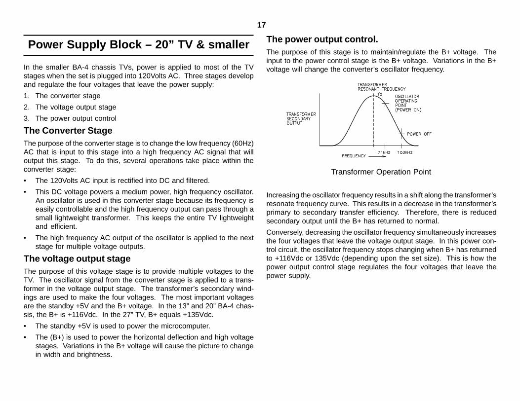
Transformer Operation Point
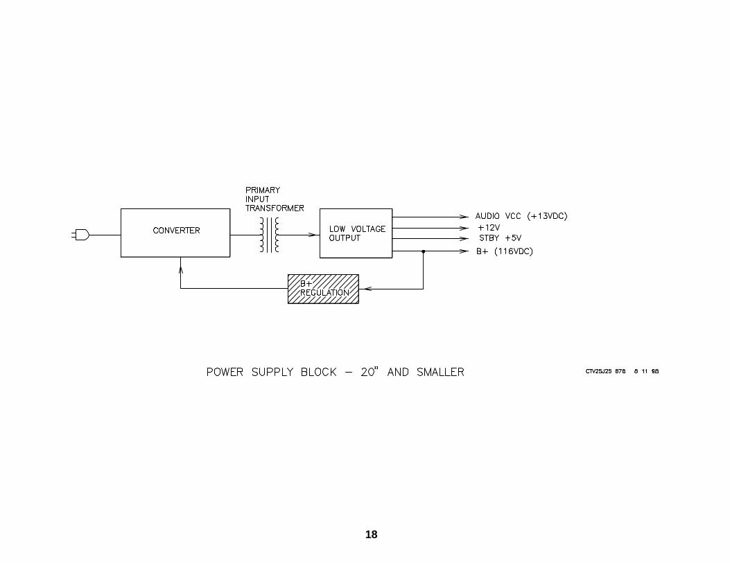
Power Supply Block – 20” TV & smaller
In the smaller BA-4 chassis TVs, power is applied to most of the TVstages when the set is plugged into 120Volts AC. Three stages developand regulate the four voltages that leave the power supply:
1. The converter stage
2. The voltage output stage
3. The power output control
The Converter StageThe purpose of the converter stage is to change the low frequency (60Hz)AC that is input to this stage into a high frequency AC signal that willoutput this stage. To do this, several operations take place within theconverter stage:
• The 120Volts AC input is rectified into DC and filtered.
• This DC voltage powers a medium power, high frequency oscillator.An oscillator is used in this converter stage because its frequency iseasily controllable and the high frequency output can pass through asmall lightweight transformer. This keeps the entire TV lightweightand efficient.
• The high frequency AC output of the oscillator is applied to the nextstage for multiple voltage outputs.
The voltage output stageThe purpose of this voltage stage is to provide multiple voltages to theTV. The oscillator signal from the converter stage is applied to a trans-former in the voltage output stage. The transformer’s secondary wind-ings are used to make the four voltages. The most important voltagesare the standby +5V and the B+ voltage. In the 13” and 20” BA-4 chas-sis, the B+ is +116Vdc. In the 27” TV, B+ equals +135Vdc.
• The standby +5V is used to power the microcomputer.
• The (B+) is used to power the horizontal deflection and high voltagestages. Variations in the B+ voltage will cause the picture to changein width and brightness.
The power output control.The purpose of this stage is to maintain/regulate the B+ voltage. Theinput to the power control stage is the B+ voltage. Variations in the B+voltage will change the converter’s oscillator frequency.
Increasing the oscillator frequency results in a shift along the transformer’sresonate frequency curve. This results in a decrease in the transformer’sprimary to secondary transfer efficiency. Therefore, there is reducedsecondary output until the B+ has returned to normal.
Conversely, decreasing the oscillator frequency simultaneously increasesthe four voltages that leave the voltage output stage. In this power con-trol circuit, the oscillator frequency stops changing when B+ has returnedto +116Vdc or 135Vdc (depending upon the set size). This is how thepower output control stage regulates the four voltages that leave thepower supply.
18

19
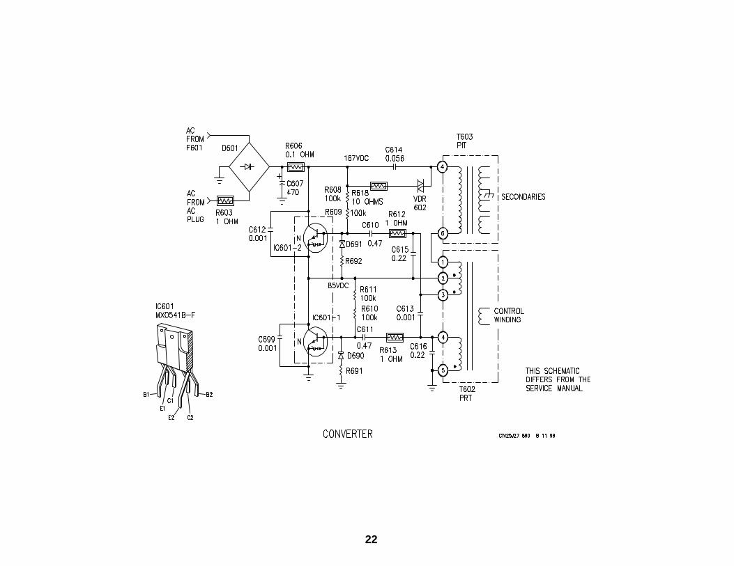
Converter
In the past, the word “converter” referred to a rotating machine consist-ing of an electric motor driving an electric generator. This system wasused to change alternating current into direct current. Changing AC toDC is also the purpose of this converter, but it is done in an electronic manner.
The converter consists of two parts:
1. The Rectifier2. The Oscillator
RectifierThe rectifier changes the 120Volts AC into DC using bridge rectifier D601.The output of D601 is a pulsating DC waveform commonly called theripple. The 60 Hz ripple has a crest (high point) and a trough (low point).C607 is the main filter capacitor that reduces the ripple amplitude bycharging during a crest and discharging to fill a void during the trough.However, as the TV’s current demand increases, C607 cannot supplythe additional current to the TV during the trough. This is why there is ahigher AC ripple across the filter capacitor during a bright scene whenthere is a greater current demand. This is shown in the chart below:
60 Hz Ripple at Main Filter Capacitor C607TV Set OFF 0.8Vp-p across C607TV Set ON – Dark screen 4Vp-p across C607TV Set ON – Bright screen 6Vp-p across C607
OscillatorThe oscillator consists of two transistors, a main transformer, a PRT powerregulator) transformer (PRT)bias and protection resistors and capacitors.When the oscillator runs, it produces a 180Vp-p square wave into themain Power Input Transformer (PIT) T603/pin 6. The two transistors(IC601) alternately turn ON and OFF to develop the square wave. Theoperation of the oscillator consists of three parts:
1. A quiescent state2. When the bottom transistor is ON and the top is OFF3. When the bottom transistor is OFF and the top is ON
The Quiescent StateThe oscillator starts when DC voltage from fusible resistor R606 is ap-plied to the oscillator stage. Two initial current paths are taken towardground within the oscillator stage. The first current path places bothtransistors in the IC601 package at the threshold of conduction to estab-lish a quiescent state. This state places 85Vdc at IC601/2’s emitter.
First Current Path to GroundComponent Input Output
R606R608 & R609 R608 R609IC601-2 Base EmitterIC601-2 Collector EmitterR611 & R610 R611 R610IC602-1 Base Emitter / GroundIC602-1 Collector Emitter / Ground
Resistors R608, R609, R611 and R610 form a voltage divider string fromthe +167Vdc supply to ground. The base – emitter junction of IC601/2connects resistors R609 and R611. R610 is connected to ground by thebase – emitter junction of IC601/1.
The voltage at the junction of R609 and R611 is approximately half thesupply voltage because the resistors in the voltage divider string are thesame value. Therefore, before oscillation begins, there are 167Volts/2 =83.5Vdc at IC601/1’s collector. At this time, the TV set consumes 40maAC (C614 removed to stop oscillation).
Bottom Transistor IC601-1 Turns ONThe second current path turns OFF transistor IC601-2 and turns ON tran-sistor IC601/1, beginning the oscillator operation. This path passesthrough several parts to ground:
Second Current Path to GroundComponent Input Output
R606C614T603 PIT Pin 4 Pin 6T602 PRT Pin 1 Pin 2R611 & R610 R611 R610IC601-1 Base Emitter / GroundIC601-1 Collector Emitter / Ground

20
21
A magnetic field is created when current flows through pins 1-2 of PRTtransformer T602. This induces a negative voltage that outputs the trans-former at T602/pin 3. This negative voltage is applied to the base ofIC601-2, turning it OFF.
At the same time, a positive induced voltage from T602/pin 4 is appliedto the base of IC601-1. This voltage is held there by capacitor C616 andcoupled to the base via C611. The positive voltage drives IC601-1 intosaturation (ON). The voltage at the collector of IC601-1 becomes zeroby transistor action. This zero volts also appears at T603/pin 6 becausethe inductance of T602 is small (few windings).
Because C614 initially acts like a momentary short, the full +167 supplyvoltage is applied to T603’s primary transformer windings (pins 4-6).T603’s rising magnetic field is coupled into the secondary windings.
Top Transistor IC601-2 Turns ONThe conduction of the transistors in the IC601 package alternate whenthe magnetic field in T603 collapses. Eventually, C616’s charge leaksoff so IC601-1 can no longer be held in conduction. At this time currentstops flowing through IC601-1 and PIT T603’s primary winding. Themagnetic field that is built up in the primary winding of T603 now col-lapses and current through the primary winding of T603 flows in the op-posite direction. During the collapsing magnetic field, current takes thispath through IC601-2:
Collapsing Magnetic Field Current PathComponent Input Output
T603/pin 4C614R608 & R609 R608 R609IC601-2 base EmitterIC601-2 collector EmitterT602 pin 2 Pin 1T603/pin 6
Both IC601 transistors receive a change in base bias. While current isflowing through T602/pins 2-1, a positive voltage is induced and outputT6502/pin 3. This is coupled into the base of IC601-2, turning it ON. Atthe same time, a negative voltage is induced and output T602/pin 4.This turns IC601-1 OFF. As a result of IC601-2’s conduction, its emitterrises to 167Vdc.
When the collapsing magnetic field in T603 has depleted its energy, thecycle repeats, starting with the charging of C614. The result is a squarewave at the junction of the two IC601 transistors when they alternatelyturn ON and OFF.
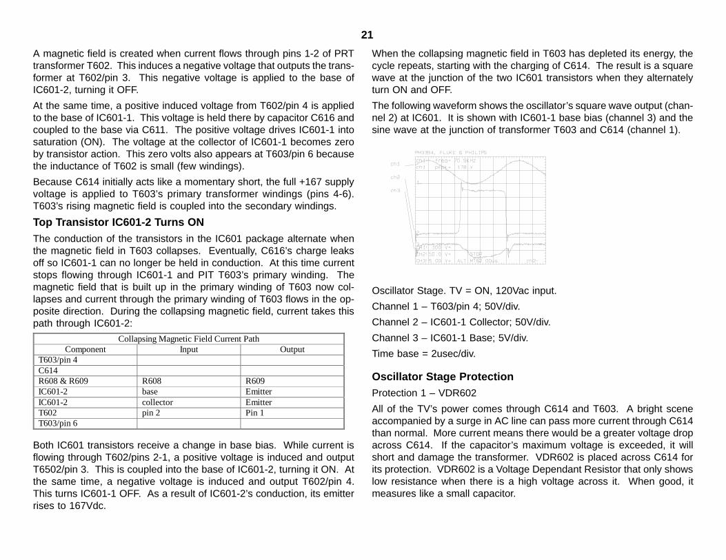
The following waveform shows the oscillator’s square wave output (chan-nel 2) at IC601. It is shown with IC601-1 base bias (channel 3) and thesine wave at the junction of transformer T603 and C614 (channel 1).
Oscillator Stage. TV = ON, 120Vac input.
Channel 1 – T603/pin 4; 50V/div.
Channel 2 – IC601-1 Collector; 50V/div.
Channel 3 – IC601-1 Base; 5V/div.
Time base = 2usec/div.
Oscillator Stage ProtectionProtection 1 – VDR602
All of the TV’s power comes through C614 and T603. A bright sceneaccompanied by a surge in AC line can pass more current through C614than normal. More current means there would be a greater voltage dropacross C614. If the capacitor’s maximum voltage is exceeded, it willshort and damage the transformer. VDR602 is placed across C614 forits protection. VDR602 is a Voltage Dependant Resistor that only showslow resistance when there is a high voltage across it. When good, itmeasures like a small capacitor.
22

23
Protection 2 – D690 & D691
The oscillator transistors (IC601) are protected from a base to emitterfailure. A transistor’s base to emitter junction can be punctured (open) orshorted. By applying an 8-10 volt reverse (b-e) bias voltage from a col-lapsing magnet field to this junction, the transistor will short. C615, C616and C613 prevent sharp (high voltage) spikes from leaving the trans-former. Diodes D690 and D691 prevent the transistor’s base to emitterjunction from being reversed.
Protection 3 – C612 & C699
A transistor’s collector to emitter junction can be shorted if the maximumvoltage across these terminals is exceeded (Vce). Although the typicalmaximum voltage for these transistors is 600volts, it can still be exceededwhen lightning brings in a much higher voltage. The voltage spikes froma non-direct lightning hit may be high in voltage, but low in current (smallpulse width). They are bypassed to ground with C612 and C699. If avery high current spike shorted IC601-2 from collector to base, currentwould also have flowed through C610 and R612 and they should bereplaced.
IC601 ProtectionProtection from internalspikes causing immediatefailure.
D690/D691 – preventsIC601’s E-B junctionfrom reverse bias damage
C615/C616/C613 –rounds off sharp spikesfrom rising and collapsingmagnetic fields.
Protection from externalspikes (lightning).
C612/C699 –high voltage low current spikes arecircumvented by this capacitor. This reduces thevoltage to IC601 so the transistor’s C-E breakdownvoltage specification is not exceeded.
Protection - Thermal R606 (fusible resistor).
Oscillator FrequencyThe oscillator frequency is predominately a function of T603 inductanceand C614 capacitance, forming a sine wave at the junction. Since theinductance of T603 is changed with a load, the frequency of the oscilla-tor will be different when the set is turned ON.
O s c i l l a t o r C h a r a c t e r i s t i c s
R e s o n a t e p a r t s : L = T 6 0 3 ( u H ) C = C 6 1 0 , C 6 1 1 , C 6 1 4 ,C 6 1 5 , C 6 1 6
F r e q u e n c y : 1 0 4 k H z .
T V O F F ( n o l o a d )
7 1 . 5 k H z .
T V O N
Oscillator TestingAfter replacing parts in this stage, check the following with an ohmmeterbefore gradually applying power:
• Shorts in T603 secondary winding loads (secondaries). Check zenerdiode D610 first (see Converter Voltage Output diagram below)
• Shorts in a flyback secondary winding loads
Testing Procedure Steps :
1. Plug the set into an isolated variable AC transformer (must containan AC ammeter and voltmeter) and set to zero volts AC.
2. Unplug the degaussing coil so the AC ammeter will only show the TVcurrent consumption.
3. Gradually increase the AC voltage to the TV while observing the fol-lowing:
• The AC current on the variable AC transformer• The oscillator supply voltage (DC) at fusible resistor R606• The DC voltage at the collector of the bottom transistor IC601-14. Gradually increase the AC voltage. The DC voltage at the collector
of IC601-1 will always be half that of the oscillator supply voltage atR606 if the oscillator is OK. This is true at any time, even when theAC voltage is being increased. The oscillator will start when there isabout 5-6Vdc at R606.

24

25
What to Expect When Increasing the AC Voltage to the TVObserve: Normal on a 20” BA-4 chassis TV
AC Current (degaussing coilunplugged)
Current will rise to 1 amp at about 12Volts AC, thendrop down to 0.34Amps
Oscillator’s DC supplyvoltage at R606
Will increase proportional to the AC voltage beingincreased.
Collector of IC601-1 Must be half the DC voltage measured at R606. Ifnot, a part is still defective.
Normal Testing ResultsBelow is a chart that shows the converter/TV operation as AC is increasedslowly to the TV that is OFF. The Degaussing coil is unplugged duringthis test.
In the 27” BA-4 chassis, the converter can be tested by temporarily jump-ing the TV’s ON/OFF relay contacts and removing the load by unsolderinga series inductor L504. Do not disconnect the B+ regulating stage (IC603,DM-58) or the TV will draw an abnormally high current as the AC voltageis increased.
Increasing Voltages with TV OFF – Model KV20M40Converter IC601-2/E
AC DC at R606 Vp-p Freq. B+7 Vac 8 Vdc 20 Vp-p 55kHz 22Vdc11 Vac 11 Vdc 28 Vp-p (w
spikes)49kHz 108Vdc
22 Vac 25 Vdc 35 Vp-p 51kHz 116Vdc40 Vac 50 Vdc 60 Vp-p 54kHz 116Vdc75 Vac 100 Vdc 100 Vp-p 61kHz 116Vdc110 Vac 150 Vdc 150 Vp-p 78.5kHz 116Vdc120 Vac 166 Vdc 170 Vp-p 104kHz 116Vdc
When beginning to increase the AC voltage to the set under test, the ACcurrent will increase sharply until the B+ reaches the correct voltage forthat set (116Vdc or 135Vdc) and then drops gradually as AC voltage isincreased. The degaussing coil is unplugged during this test.
Peak AC Current ConsumptionModel AC Voltage AC CurrentKV20M40 12Vac 0.8 AmpsKV27S45 11Vac 1.3 Amps
Above 12Vac, the B+ has reached its maximum and the regulation stagechanges the converter frequency to supply sufficient TV current to main-tain a steady B+ voltage. As the input AC is being increased toward120Vac, the current continues to drop toward the normal operating level.This TV power supply can run unloaded, but the regulation circuit mustremain intact or the unit will damage the converter IC601 and blow afuse.

26

27
NOTES

28
29
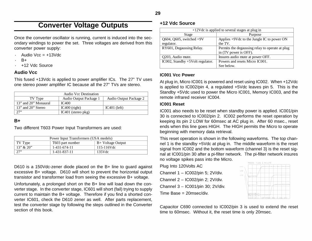
Converter Voltage Outputs
Once the converter oscillator is running, current is induced into the sec-ondary windings to power the set. Three voltages are derived from thisconverter power supply:
· Audio Vcc = +13Vdc· B+· +12 Vdc Source
Audio VccThis fused +13Vdc is applied to power amplifier ICs. The 27” TV usesone stereo power amplifier IC because all the 27” TVs are stereo.
Audio Vcc DestinationTV Type Audio Output Package 1 Audio Output Package 2
13” and 20” Monaural IC40013” and 20” Stereo IC400 (right) IC401 (left)27” IC401 (stereo pkg)
B+Two different T603 Power Input Transformers are used:
Power Input Transformers (USA models)TV Type T603 part number B+ Voltage Output13” & 20” 1-431-674-11 115-116Vdc27” 1-431-837-11 135Vdc
D610 is a 150Vdc-zener diode placed on the B+ line to guard againstexcessive B+ voltage. D610 will short to prevent the horizontal outputtransistor and transformer load from seeing the excessive B+ voltage.
Unfortunately, a prolonged short on the B+ line will load down the con-verter stage. In the converter stage, IC601 will short (fail) trying to supplycurrent to maintain the B+ voltage. Therefore if you find a shorted con-verter IC601, check the D610 zener as well. After parts replacement,test the converter stage by following the steps outlined in the Convertersection of this book.
+12 Vdc Source+12Vdc is applied to several stages at plug in
Stage PurposeQ604, Q605, switched +9Vregulator.
Applies +9Vdc to the Jungle IC to power ONthe TV.
RY601, Degaussing Relay. Permits the degaussing relay to operate at plugin (TV power is OFF).
Q203, Audio mute. Insures audio mute at power OFF.IC002, Standby +5Volt regulator. Powers and resets Micro IC001.
See below.
IC001 Vcc Power
At plug in, Micro IC001 is powered and reset using IC002. When +12Vdcis applied to IC002/pin 4, a regulated +5Vdc leaves pin 5. This is theStandby +5Vdc used to power the Micro IC001, Memory IC003, and theremote infrared receiver IC004.
IC001 Reset
IC001 also needs to be reset when standby power is applied. IC001/pin30 is connected to IC002/pin 2. IC002 performs the reset operation bykeeping its pin 2 LOW for 60msec at AC plug in. After 60 msec., resetends when this line goes HIGH. The HIGH permits the Micro to operatebeginning with memory data retrieval.
This reset operation is shown in the following waveforms. The top chan-nel 1 is the standby +5Vdc at plug in. The middle waveform is the resetsignal from IC002 and the bottom waveform (channel 3) is the reset sig-nal at IC001/pin 30 after a pi-filter network. The pi-filter network insuresno voltage spikes pass into the Micro.
Plug Into 120Volts AC
Channel 1 – IC002/pin 5; 2V/div.
Channel 2 – IC002/pin 2; 2V/div.
Channel 3 – IC001/pin 30; 2V/div.
Time Base = 20msec/div.
Capacitor C690 connected to IC002/pin 3 is used to extend the resettime to 60msec. Without it, the reset time is only 20msec.

30

31
IC001 Memory Data Retrieval
After reset, one of IC001’s first programs is to retrieve data from theexternal EEProm memory IC003. Data and clock are output IC001/pins36 and 38 to request a reading of all the memory information. The memoryinformation is serially output IC003/pin 5 and stored in Micro IC001’sresident memory (internal RAM). This memory information contains:
· The user’s picture and sound preferences;· The last active TV station information; and· The TV operating parameters (height, width, linearity, OSD position,
etc).Each time the user’s preferences and channel are changed, the MicroIC001 loads these changes into memory IC003.
Micro IC001 and Memory IC003 communications occur during these times:
Micro – Memory CommunicationsWhen Direction Purpose
Plug In To Micro Load user and operating parameters intoworking RAM in IC001.
User commandchange
To Memory Each time the user changes a preference (likevolume, or channel number).

32
33
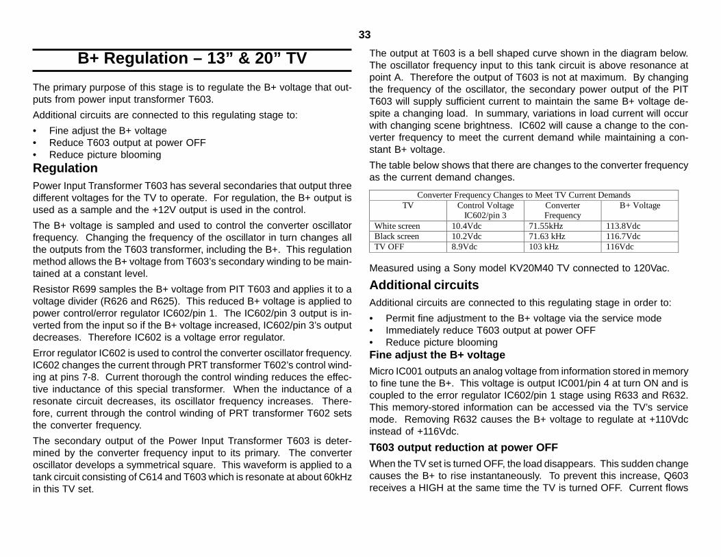
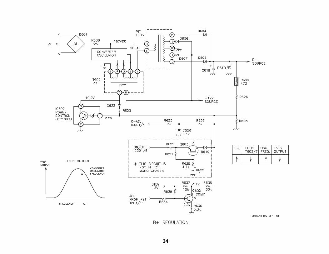
B+ Regulation – 13” & 20” TV
The primary purpose of this stage is to regulate the B+ voltage that out-puts from power input transformer T603.
Additional circuits are connected to this regulating stage to:
• Fine adjust the B+ voltage• Reduce T603 output at power OFF• Reduce picture bloomingRegulationPower Input Transformer T603 has several secondaries that output threedifferent voltages for the TV to operate. For regulation, the B+ output isused as a sample and the +12V output is used in the control.
The B+ voltage is sampled and used to control the converter oscillatorfrequency. Changing the frequency of the oscillator in turn changes allthe outputs from the T603 transformer, including the B+. This regulationmethod allows the B+ voltage from T603’s secondary winding to be main-tained at a constant level.
Resistor R699 samples the B+ voltage from PIT T603 and applies it to avoltage divider (R626 and R625). This reduced B+ voltage is applied topower control/error regulator IC602/pin 1. The IC602/pin 3 output is in-verted from the input so if the B+ voltage increased, IC602/pin 3’s outputdecreases. Therefore IC602 is a voltage error regulator.
Error regulator IC602 is used to control the converter oscillator frequency.IC602 changes the current through PRT transformer T602’s control wind-ing at pins 7-8. Current thorough the control winding reduces the effec-tive inductance of this special transformer. When the inductance of aresonate circuit decreases, its oscillator frequency increases. There-fore, current through the control winding of PRT transformer T602 setsthe converter frequency.
The secondary output of the Power Input Transformer T603 is deter-mined by the converter frequency input to its primary. The converteroscillator develops a symmetrical square. This waveform is applied to atank circuit consisting of C614 and T603 which is resonate at about 60kHzin this TV set.
The output at T603 is a bell shaped curve shown in the diagram below.The oscillator frequency input to this tank circuit is above resonance atpoint A. Therefore the output of T603 is not at maximum. By changingthe frequency of the oscillator, the secondary power output of the PITT603 will supply sufficient current to maintain the same B+ voltage de-spite a changing load. In summary, variations in load current will occurwith changing scene brightness. IC602 will cause a change to the con-verter frequency to meet the current demand while maintaining a con-stant B+ voltage.
The table below shows that there are changes to the converter frequencyas the current demand changes.
Converter Frequency Changes to Meet TV Current DemandsTV Control Voltage
IC602/pin 3ConverterFrequency
B+ Voltage
White screen 10.4Vdc 71.55kHz 113.8VdcBlack screen 10.2Vdc 71.63 kHz 116.7VdcTV OFF 8.9Vdc 103 kHz 116Vdc
Measured using a Sony model KV20M40 TV connected to 120Vac.
Additional circuitsAdditional circuits are connected to this regulating stage in order to:
• Permit fine adjustment to the B+ voltage via the service mode• Immediately reduce T603 output at power OFF• Reduce picture bloomingFine adjust the B+ voltageMicro IC001 outputs an analog voltage from information stored in memoryto fine tune the B+. This voltage is output IC001/pin 4 at turn ON and iscoupled to the error regulator IC602/pin 1 stage using R633 and R632.This memory-stored information can be accessed via the TV’s servicemode. Removing R632 causes the B+ voltage to regulate at +110Vdcinstead of +116Vdc.
T603 output reduction at power OFFWhen the TV set is turned OFF, the load disappears. This sudden changecauses the B+ to rise instantaneously. To prevent this increase, Q603receives a HIGH at the same time the TV is turned OFF. Current flows
34
35
through its emitter-base junction, R628 and C625, to ground. Q603 turnsON increasing the voltage at error regulator IC602/pin 1. This results ina decrease in T603 output to offset the no load condition at power OFF.
Reduce picture bloomingPicture blooming can occur when a bright scene is called for. This scenecauses the TV to draw the largest amount of power from the power sup-ply at once. When the power supply is delivering the maximum amountof current, it is functioning at the very top of the bell curve in the non-linear region. At this operating point, the B+ regulation does not exist.The picture may stretch disproportionately (blooming) as the B+ fluctu-ates.
To avoid this, Q602 monitors the ABL voltage from the flyback trans-former secondary. A bright scene causes this ABL voltage to decrease.Q602 inverts this change and a positive going change is applied to theerror regulator IC602/pin 1. This results in a reduction of T603 output,shifting the operating point away from the top of the bell curve. Thisreestablishes regulation at very bright scene levels. Picture blooming asa result of no regulation is reduced.
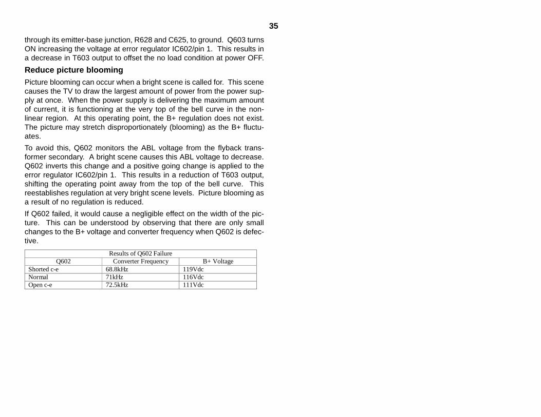
If Q602 failed, it would cause a negligible effect on the width of the pic-ture. This can be understood by observing that there are only smallchanges to the B+ voltage and converter frequency when Q602 is defec-tive.
Results of Q602 FailureQ602 Converter Frequency B+ Voltage
Shorted c-e 68.8kHz 119VdcNormal 71kHz 116VdcOpen c-e 72.5kHz 111Vdc

36
37
Power Supply Block – 27” Models
13” and 20” Sony Electronics BA-4 chassisIn the 13” and 20” Sony Electronics BA-4 chassis TV sets, the converteroscillator runs when the set is plugged in. Only the “Set +9V” is switchedON to turn ON the TV.
27” Sony Electronics BA-4 chassisThe 27” model of the BA-4 chassis is a bit more conventional. Only thestandby power supply is active when this TV is plugged in. This standby+7.5 is regulated down to standby +5V. Standby +5 voltage is used topower the Micro and Infrared receiver so it can respond to a power ONcommand from the user.
When the Micro receives a power ON command, first the degaussingcircuitry becomes active. While this circuit operates, the power relay isenergized. This relay delivers AC power to the converter stage whichoutputs B+, +12Vdc, and audio Vcc (+13Vdc) to power up the TV.
This standby power supply is new to the consumer TV line. It contains aFET based oscillator that can operate over a wide range of input volt-ages.

38

39
Standby Power Supply
This standby power supply is new to the consumer TV line. It contains aFET based oscillator circuit that can operate over a wide range of inputvoltages, but it must have a load.
Standby Oscillator Normal Operating ConditionsTV 7.5Vdc Load current Frequency @ Q5001/D
ON 130 ma 42kHzOFF 30 ma 74kHzStandby 7.5Vdc outputnot loaded.
0 ma(load unplugged)
Dampened ringing at 79kHz.
There are several stages that make up this oscillator circuit:
• Basic oscillator• Voltage regulator• Current limiter• Additional components
Basic OscillatorFor this oscillator to work, FET Q5001 is turned ON and OFF with the aidof the standby transformer T5001.
FET Q5001 - ONFET Q5001 is turned ON when a positive voltage appears at its gate.The voltage comes from fusible resistor R5001 and passes through T5001/pins 1-3 and R5003 to arrive at Q5001’s gate. As the gate voltage in-creases, the FET drain to source resistance decreases. Q5001’s cur-rent flows from T5001/pin 1-3 through the drain to source of Q5001 thor-ough R5011 to ground:
I n i t ia l C u r re n t P a th to G ro u n d
In p u t O u tp u t
T 5 0 0 1 S B T P in 1 P in 3
Q 5 0 0 1 D ra in S o u rc e
R 5 0 1 1 G ro u n d
Current flowing thorough transformer SBT T5001/pins 1-3 induces volt-ages into the other windings. A positive voltage leaves T5001/pin 4,through C5004 to Q5001’s gate. This positive voltage keeps the FETON. This second turn ON voltage is necessary because while Q5001 isin conduction, the original turn ON voltage from R5003 has dropped tozero.
This waveform shows the gradual conduction of Q5001 (drain voltagedecreasing in channel 1) as its gate voltage increases (channel 3) toabout 2.3Vdc.
Model KV27S45 TV is OFF.
Channel 1 - Q5001/Drain; 100V/div
Channel 2 – T5001/pin 4; 10V/div.
Channel 3 - Q5002/collector; 2V/div.
Channel 4 - Q5002/base; 0.5V/div.
Time base = 2usec/div.
FET Q5001 – OFFAt the beginning of the ½ cycle, the positive voltage at Q5001’s gatedecays. This is because C5004’s charge has leaked off. The reducedQ5001’s gate voltage begins to turn Q5001 OFF so its drain voltagerises.

40

41
When FET Q5001 is turned OFF, its drain voltage rises above the 164Vdc-supply voltage (to about +300Vdc). This is because magnetic energystored in the SBT T5001 winding collapses. The reversed current flowapplies a positive voltage to charge C5003 via D5003:
Current Path from T5001’s Collapsing Magnetic FieldPart Input Output
T5001 Pin 3D5003 Anode CathodeC5003T5001 Pin 1
T5001’s collapsing magnetic field induces a LOW voltage that is outputpin 4 to Q5001/gate. This LOW insures that Q5001 turns OFF. In thispath, C5003 is charged to about 300Vdc, representing the crest of theoscillator waveform (at Q5001/drain).
Voltage RegulatorTo maintain voltage regulation, the following parts are used:
P a rts U s e d fo r V o lta g e R e g u la t io n
P a rt P u rp o s e
D 5 0 0 7 R e c t if ie s T 5 0 0 1 s a m p le v o lta g e
D 5 0 0 6 – 5 .6 V z e n e r K e e p s Q 5 0 0 2 O F F s o Q 5 0 0 1 c a nb e g in o s c il la t in g .
Q 5 0 0 2 – N P N C o n tr o ls th e v o lt a g e a t th e g a t e o fQ 5 0 0 1 fo r r e g u la t io n
When the oscillator is running, the voltage at T5001/pin 6 is sampledand rectified. This sampled voltage passes through zener D5006 and isapplied to error regulator Q5002. When the standby voltage is high,more current is applied to Q5002/base. Its increased conduction re-duces the Q5001 gate voltage and the FET stays in conduction less.This change in duty cycle decreases the power available at the SBTT5001 secondary and the voltage is reduced.
Current LimiterThe current through Q5001 is limited by reducing its gate voltage. SinceQ5001 and R5011 are in series, the current flowing through R5011 rep-resents the current in the FET. If the current through R5011 drops 0.6Vdc,Q5002 begins to conduct. Its conduction reduces the FET gate voltagelimiting its current so it does not overheat.
Additional ComponentsThere are several additional components used in this circuit that havenot been discussed:
Additional ComponentsParts Purpose
D5005, R5009, C5008,C5006
Back up for voltage error regulator. Prevents excessivestandby voltage. These parts limit the 7.5Vdc to 33Vdc ifthe main regulator path (D5007, R5012, or D5006)opened.
D5004, R5008 Keeps Q5002 OFF at the start up of the next oscillatorcycle.
TestingAfter replacing the Q5001 FET, and checking for shorts, increasing theAC voltage gradually is a good way to determine if there is an additionalproblem. The standby power supply is still connected to the load duringthis test so you must monitor the 7.5Vdc output voltage and prevent itfrom being excessive. The oscillator should start at about 35Vac. Thenormal operating voltages are listed in the chart below:
Normal Standby Oscillator Characteristics – KV27S45AC Voltage R5001 Vdc Q5001/D Osc. Freq. Output Vdc
20Vac 8.5Vdc 0 0 040Vac 47Vdc 180Vp-p 29.3kHz 7.4Vdc60Vac 79Vdc 200Vp-p 50 kHz 7.56Vdc80Vac 108Vdc 240Vp-p 61.6 kHz 7.6Vdc100Vac 136Vdc 270Vp-p 69.6 kHz 7.6Vdc120Vac 164Vdc 300Vp-p 74.2 kHz 7.6Vdc

42

43
NOTES

44

45
B+ Regulation – 27” TV
The primary purpose of this stage is to regulate the B+ voltage that out-puts from power input transformer T603. The B+ voltage will remain at astable +135Vdc because of this regulating circuit.
A soft start circuit is connected to this regulating stage to keep the B+from rising above +135Vdc at power ON before the regulating circuit hashad time to react.
RegulationPower Input Transformer T603 has several secondaries that output threedifferent voltages for the TV to operate. For regulation, the B+ output isused as a sample and the +12V output is used in the control.
The B+ voltage is sampled and used to control the converter oscillatorfrequency. Changing the frequency of the oscillator in turn changes allthe outputs from the T603 transformer, including the B+. This regulationmethod allows the B+ voltage from T603’s secondary winding to be main-tained at a constant level.
Resistor R699 samples the B+ voltage from PIT T603 and applies it topower control/error regulator IC603/pin 1. The IC602/pin 4 output is in-verted from the input so if the B+ voltage increased, IC602/pin 4’s outputdecreases. Therefore IC603 is seen now as an error regulator.
Error regulator IC603 is used to control the converter oscillator frequency.IC603 changes the current through PRT transformer T602’s control wind-ing at pins 7-8. Current thorough the control winding reduces the effec-tive inductance of this special transformer. When the inductance of aresonate circuit decreases, its oscillator frequency increases. There-fore, current through the control winding of PRT transformer T602 setsthe converter frequency.
The secondary output of the Power Input Transformer T603 is deter-mined by the converter frequency input to its primary. The converteroscillator waveform is applied to a tank circuit consisting of C614 andT603 which is resonate at about 60kHz in this TV set. T603’s output is abell shaped power curve shown in the diagram. The oscillator frequencyinput to this tank circuit is to the right of the resonance peak at point A.
Therefore the output of T603 is not at maximum. By changing the fre-quency of the oscillator, the secondary power output of the PIT T603 canbe adjusted to provide sufficient load current while maintaining the sameB+ voltage. This is why IC603 is labeled a power control device.
Soft Start CircuitThe soft start circuit consists of Q608, C632 and the PRT transformerT602. Its purpose is to keep the B+ voltage initially low at power ON.
When the TV is turned ON, the following devices energize the powerrelay, supplying power to the converter oscillator.
T V P o w e r O N
D e v ic e S ta te
M ic ro IC 0 0 1 /p in 6 L O W
Q 6 0 4 O F F (c o lle c to r is + 7 .5 V d c )
Q 6 7 0 O N (c o lle c to r is 0 .3 V d c )
R Y 6 0 2 E n e rg iz e d (c o n ta c ts c lo s e d )
When power is applied to the converter oscillator, voltage is output thesecondaries of PIT T603. Current from D606 and D607 (+12V source)takes the following path to ground:
Soft Start PathPart Input Output
D606 & D607 Anode Cathode (band end)R622T602 PRTQ608 Emitter BaseC632 + -Q608 Emitter Collector (ground)
This path causes current to flow through T602’s control winding at pins7-8. Current flow in this control winding causes the converter oscillatorfrequency to shift to a higher frequency at start up. This keeps the B+voltage low so it does not rise above +135Vdc at power ON.

46
47
Power ON/Communications Block
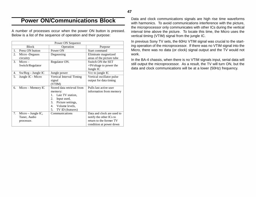
A number of processes occur when the power ON button is pressed.Below is a list of the sequence of operation and their purpose:
Power ON SequenceBlock Operation Purpose
1. Press ON button Power ON Start command2. Micro -Degauss
circuitryDegaussing Eliminate magnetized
areas of the picture tube3. Micro –
Switch/RegulatorRegulator ON. Switch ON the SET
+9Voltage to power theJungle IC
4. Sw/Reg – Jungle IC Jungle power Vcc to jungle IC5. Jungle IC - Micro Vertical Interval Timing
signal(VTIM)
Vertical oscillator pulseoutput for data timing
6. Micro – Memory IC Stored data retrieval frommemory:1. Last TV station,2. Input used,3. Picture settings,4. Volume levels,5. TV ID (features)
Pulls last active userinformation from memory
7. Micro – Jungle IC,Tuner, Audioprocessor.
Communications Data and clock are used tonotify the other ICs toreturn to the former TVcondition at power down
Data and clock communications signals are high rise time waveformswith harmonics. To avoid communications interference with the picture,the microprocessor only communicates with other ICs during the verticalinterval time above the picture. To locate this time, the Micro uses thevertical timing (VTIM) signal from the jungle IC.
In previous Sony TV sets, the 60Hz VTIM signal was crucial to the start-ing operation of the microprocessor. If there was no VTIM signal into theMicro, there was no data (or clock) signal output and the TV would notwork.
In the BA-4 chassis, when there is no VTIM signals input, serial data willstill output the microprocessor. As a result, the TV will turn ON, but thedata and clock communications will be at a lower (50Hz) frequency.

48

49
Degaussing Circuitry
ConceptThe picture tube has three electron beams that are targeted to exactlocations on the phosphor screen. If a magnet were brought near thepicture tube, the electron beams would be attracted to it. The electronbeams would move out of place and not land on their correct phosphors.When they strike the wrong phosphors, a predominate color pattern ap-pears at that portion of the screen near the magnet. If only one electronbeam is turned ON, the TV screen will not display a pure single colorscreen. This is called a purity problem.
Placing speakers next to the TV commonly causes purity problems. Themagnets within the speakers disturb the beam landing. However, theinternal speaker’s magnet is fully shielded to prevent this problem.
Electrical appliances that contain motors, placed near the TV or turnedOFF at the TV, will also cause a purity problem. In this case, turning OFFthe appliance magnetizes metal areas of the picture tube’s aperture grillcausing the purity problem.
The earth’s terrestrial magnetism can also magnetize parts of the picturetube’s aperture grill when the TV is moved. The degaussing circuit elimi-nates these magnetic effects on the aperture grill.
The purpose of this degaussing circuit is to demagnetize the aperturegrill at plug in and each time the TV is powered ON. This is done bypassing AC through a coil of wire located at the bell of the picture tube.The AC field created eliminates the magnetized areas of the aperturegrill.
Circuit OperationMicro IC001 controls the degaussing relay. At plug in, Micro IC001 hasreceived standby +5Vdc and a LOW at IC001/pin 30 for reset. After thereset line goes HIGH, IC001 can respond to the Power ON command.Immediately the degaussing output line at IC001/pin 13 goes HIGH tostart degaussing. This HIGH is applied to Q601’s base, turning the tran-sistor ON. Current flowing through Q601 also flows through the RY601relay coil, energizing the degaussing relay.
AC current from the 120Vac line can pass through the relay into thedegaussing coil. The 120Vac input must first pass through several partsbefore reaching the degaussing coil:
Parts between the AC Line and the Degaussing CoilPart Purpose
VDR601 Absorbs voltage spikes from the AC line.C601 Reduces voltage spikes from the line and from the
TV (converter stage).R620 Bleeder resistor for C601T601 Common mode rejection transformer. Cancels
opposite polarity noise signals on the AC line.THP6013.5 ohms cold14kohms hot (calculated)
Degaussing thermistor is 3.5 ohms cold in series withthe degaussing coil. It increases in resistance toalmost turn OFF all the coil current within 2 seconds.
RY601Coil = 273 ohms
Controlled by IC001 to apply AC to the degaussingcoil for 2.2 seconds.
Degaussing coilApprox. 8 ohms
Creates an AC field that erases magnetic effects ofthe aperture grill.
Thermistor OperationWhen current flows through the degaussing coil, it also flows through theTHP601 thermistor. Initially its resistance is 3.5 ohms, but increasesrapidly so that within two seconds there is only 8.5ma flowing throughthe degaussing coil. This current develops a negligible magnetic field inthe coil and is effectively OFF. Shortly after the thermistor has reachedits highest resistance, the RY601 relay disconnects the degaussing coilfrom the AC line completely.
Degaussing Coil CurrentPower ON 10Amps (momentary)1.7 seconds after power ON 8.5ma. (thermistor operation THD601)2.2 seconds after power ON 0 ma.

50

51
NOTES

52

53
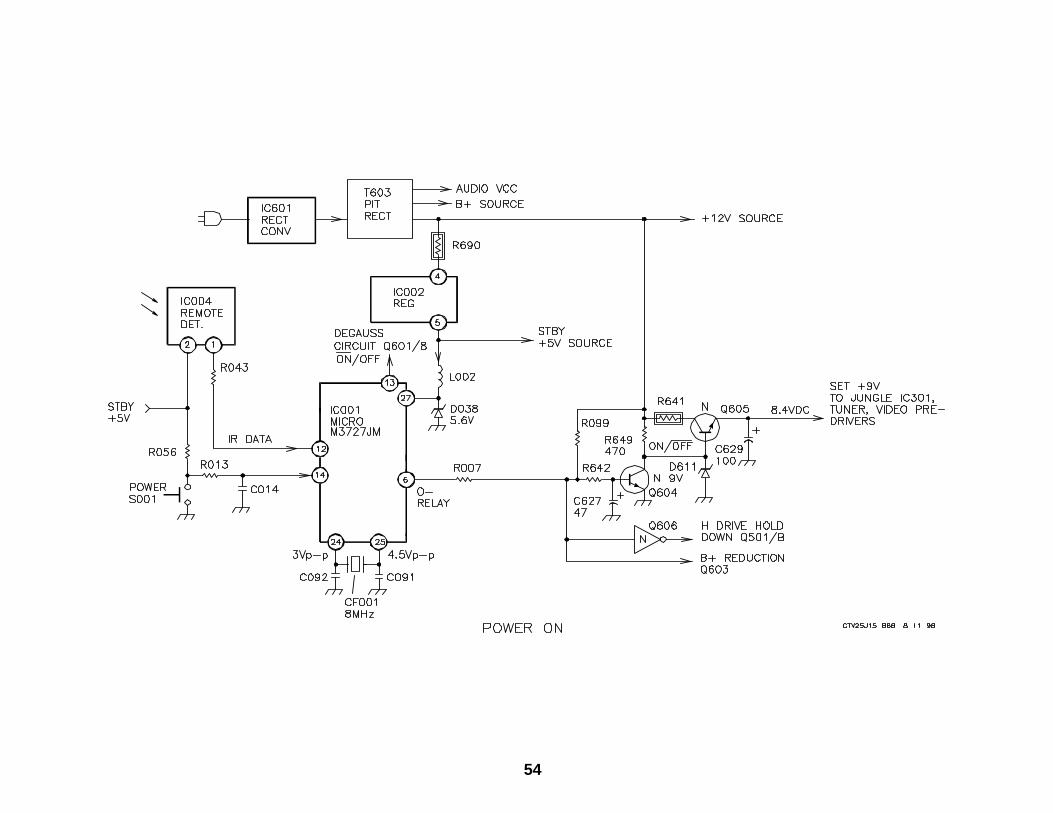
Power ON
Power ON
Once the Micro has received Standby +5Vdc at plug in, the external8MHz crystal can run (even while reset). This 8MHz is used for all se-quential digital based operations in IC001 and consequently is neces-sary for any activity.
Now that the Micro is ready, it can respond to a power ON command.The ON command can come from the front panel S001 switch or theremote control. Either input causes IC001 to respond at the followingoutputs:
Micro Output at Power ONOutput Purpose
1. IC001/pin 13 = LOW Activates the degaussing circuit2. IC001/pin 6 = LOW Turns ON the Set +9V regulator Q605
The LOW output from IC001/pin 13 is applied to the degaussing circuitry.It only remains LOW for 2.2 seconds each time the TV is turned ON.This is more than enough time needed for the degaussing operation.
The LOW output at IC001/pin 6 is applied to Q604 and Q605. It remainsLOW as long as the set is ON. The LOW is applied to the base of switchQ604, turning it OFF.
With Q604 turned OFF, its collector voltage is allowed to rise to the zenervoltage of D611 (+9Vdc). The zener voltage comes from pull up resistorR649 connected to the +12 volt source. The +9Vdc back at the zenerdiode’s cathode is connected to the base of regulator Q605. The posi-tive voltage will forward bias Q605 so its emitter will output “Set +9V”(actually +8.4Vdc). This Set +9V is the source of Vcc power for theJungle IC to begin the TV set operation.
Circuits Used During Power OFFTransistor Name Purpose
Q606 Horizontal Drive HoldDown
Grounds the horizontal drive toassure no FBT secondaryvoltages.
Q603 B+ Reduction Prevents excessive B+ when thereis no load at power OFF
Power OFFAdditional circuits connected to IC001/pin 6 are used during power OFFto insure proper turn OFF. This is because only the Set +9Vdc is re-moved at power OFF while the remaining converter voltages are presentto many circuits.
54

55
NOTES

56

57
Communications
Before normal communications can begin, start-timing pulses are needed.Then Data and Clock (I2C) communications will run as long as the set ispowered ON.
StartOnce the TV is powered ON, Set +9Vdc is available to the Y/C JungleIC301 at pin 44. Then IC301’s internal oscillator starts, making horizon-tal and vertical drive signals and a 60Hz Vertical Timing (VTIM) pulsefrom pin 5. This 60Hz VTIM pulse begins the communications by tellingIC001 when to begin sending out Data and Clock signals.
RunMemory RetrievalMicro IC001 first communicates with the memory IC003. TV settingswere stored into memory IC003 the each time they are changed whilethe TV was ON. At power ON, IC001 sends out clock and data commu-nications to Memory IC003 to retrieve this information. The return data issent back to IC001 on the same data line (IC001/pin 36 – IC003/pin 5)and is supported by clock signal from IC001/pin 39.
User Settings Transferred from Memory
The user settings stored in memory will include:
• TV station – last station used, CC, channel block, favorites• Input Selection - Video 1, Video 2, or TV input• Picture settings – Brightness, color, sharpness, etc. (if not at default
level)• Volume – level, tone, balance, speaker ON/OFFThe waveform of the VTIM signal is shown preceding the IC003 memorydata and clock signals.
TV ON - Active channel.
Channel 1 – IC301/pin 5; VTIM
Channel 2 – IC001/pin 36; Bi-directional Data
Channel 3 – IC001/pin 39; Clock Output to IC003
Channel 4 – IC001/pin 37; Bi-directional Data
All waveforms at 5V/div.; Time base = 2msec/div.
ID Code Transferred from Memory
In addition to the user data transferred from memory into IC001, operat-ing parameters such as size, gamma, linearity, and the TV’s ID codes arealso transferred.
These ID codes identify the model’s features. Having the wrong codeswill permit the TV to display parts of a feature that does not exist in thatmodel. For instance, a video 3 may appear on the OSD when there is novideo 3 input. These ID codes are accessible for check and correctionfrom the service menu (see the service manual for access informationfrom the remote control).

58
59
Below is a chart showing the ID codes for the current BA-4 chassis.
ID C o d e s fo r th e B A -4 C h a s s is
M o d e l
K V -
ID -0 *
C o u n t ry
ID -1 ID -2
S te re o
ID -3 ID -4 ID -5 ID -6 ID -7
1 3 M 4 0 2 5 1 0 3 1 9 0
1 3 M 5 0/5 1
2 5 3 0 3 1 9 1
2 0 M 4 0 2 5 3 0 1 3 1 2 3 1
2 0 S 4 0 /4 1
2 5 3 1 1 3 1 2 3 1
2 0 V 8 0 2 5 1 9 1 3 1 3 1 3 1 1
2 7 S 4 0 1 5 3 1 1 3 1 9 5 3 1 1 0 6 4
2 7 S 4 5 1 5 3 2 7 1 3 1 9 5 3 1 1 1 6 4
2 7 S 6 5 1 5 3 2 7 2 7 1 5 1 9 5 3 1 7 6 4
* T h e C a n a d ia n v e r s io n is a 9 in s te a d o f 2 5 a n d 1 2 9 in s te a d o f 1 5 3 .
Communications with other ICs
After the memory IC003 information is stored in the working static memoryinside IC001, the information is communicated to the Jungle IC301, TunerTU101, and audio processor (IC402 if used) to set up all the operatingparameters of the TV.
In this second scope shot, the same data is shown expanded so you cansee there is a space in the clock signal from IC001. It also can be seenthat the memory data and jungle data seem to be alike.
TV ON - Active channel.
Channel 1 – IC301/pin 5; VTIM
Channel 2 – IC001/pin 36; Bi-directional Data
Channel 3 – IC001/pin 39; Clock Output to IC003
Channel 4 – IC001/pin 37; Bi-directional Data
All waveforms at 5V/div.; Time base = 200usec/div.
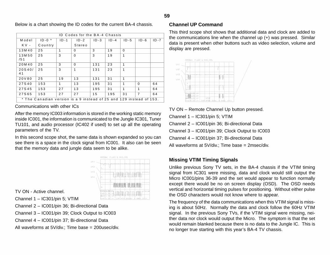
Channel UP CommandThis third scope shot shows that additional data and clock are added tothe communications line when the channel up (+) was pressed. Similardata is present when other buttons such as video selection, volume anddisplay are pressed.
TV ON – Remote Channel Up button pressed.
Channel 1 – IC301/pin 5; VTIM
Channel 2 – IC001/pin 36; Bi-directional Data
Channel 3 – IC001/pin 39; Clock Output to IC003
Channel 4 – IC001/pin 37; Bi-directional Data
All waveforms at 5V/div.; Time base = 2msec/div.
Missing VTIM Timing SignalsUnlike previous Sony TV sets, in the BA-4 chassis if the VTIM timingsignal from IC301 were missing, data and clock would still output theMicro IC001/pins 36-39 and the set would appear to function normallyexcept there would be no on screen display (OSD). The OSD needsvertical and horizontal timing pulses for positioning. Without either pulsethe OSD characters would not know where to appear.
The frequency of the data communications when this VTIM signal is miss-ing is about 50Hz. Normally the data and clock follow the 60Hz VTIMsignal. In the previous Sony TVs, if the VTIM signal were missing, nei-ther data nor clock would output the Micro. The symptom is that the setwould remain blanked because there is no data to the Jungle IC. This isno longer true starting with this year’s BA-4 TV chassis.

60

61
Video Processing Block
TunerThe Micro controls the tuner through the use of data and clock communi-cations. Both share in the TV station tuning functions:
TV Tuning FunctionsMicro Tuner
Data output identifies TV bands(Low/high VHF, UHF, Cable) and TVchannel.
Uses input data to change the internallocal oscillator frequency for stationselection.
Data output uses AFT feedback to fine-tune the TV station.
Outputs center of station AFT voltage.
Uses TV video sync to ID an active TVstation (auto programming).
Outputs TV video and audio signal
Memorizes the location of active TVstations (external memory IC).
Video InputsIn the 20” and smaller screen size BA-4 chassis, video input selection isperformed by the Jungle IC. As many as three video inputs are availablefor the user to select from:
• Tuner video• Video 1 – composite or S video• Video 2 – composite video onlyWhen the S video 1 jack is present in a model, the composite video 1input signal must pass through the S video jack. The composite video 1signal leaves the jack at the luminance (Y) line to the Jungle IC. When Svideo 1 is input, the round S video plug grounds the SW input to theJungle IC so it knows to route the separate Y and C inputs differently.
In the 27” screen BA-4 chassis, there maybe an additional video inputand video output jack. Therefore, a video switcher IC is used beforeentering the Y/C Jungle IC as composite video or Y & C (S video).
Digital Comb FilterSome TV models have a digital comb filter connected to the Y/C JungleIC. These models must be identified to the Jungle IC so it knows to routecomposite video (V) out to the filter and receive luminance (Y) / color (C)information from the filter as a departure from the internal video-process-ing path. Data from the Micro identifies the presence of the externalcomb filter. This data comes from ID codes found in the Micro and memoryIC. The technician can access them from the service mode (further infor-mation is in the service manual).
The purpose of a comb filter is to separate a composite video signal’sluminance (Y) information from its color (C) information. Digital combfilters have gone further. There are currently four types of comb filtersavailable on the TV market:
1. Analog Comb Filter - This type of filter will help increase the pictureresolution to above 330 lines.
2. Digital Comb Filter – This performs the same function, but the sepa-ration is done in the digital domain.
3. Digital 2-D Adaptive Comb Filter – This filter employs a memory toanalyze the picture information in two dimensions (2-D), verticallyand horizontally.The result is not only Y/C separation, but also higher resolution thana standard digital comb filter by simulating detail and reduction of dotcrawl. The word “Adaptive” indicates that the digital processing isconstantly analyzing and selecting the best algorithm available in thefilter.
4. Digital 3-D Adaptive Comb Filter – This filter is an improvement overthe 2-D that only processed information within that field. The 3-Dfilter analyzes information over frames to compare and eliminate noise,interference and irregularities, as well as separate the Y from the C.
Different digital filters are used in different models of Sony TVs.

62
63
Video OutputThe video processing continues from within the Y/C Jungle to the picturetube. The Y/C jungle IC takes the composite video or S video and con-verts this information into separate R, G and B voltage levels. Thesevoltages are amplified by the video output stage and applied to the pic-ture tube cathodes.
On Screen Display
The TV’s menu, channel information and input selected are introducedinto the video path in the last stages of the Jungle IC. This alphabetcharacter information is called On Screen Display information (OSD). Itcomes from the Micro and is sent to the Jungle IC as OSD voltages.Since the Microprocessor needs to know exactly where to place thesecharacters, it is essential that horizontal (HP) and vertical (VTIM) timingpulses are input or there will be no OSD.
IK Sense Circuit
The Jungle IC adjusts the levels of each R, G and B signal to maintain alevel of white balance. The current drawn by each picture tube cathodeis monitored as long as the TV set is ON. The monitoring process resultsin three pulses that reside in the vertical blanking (invisible) area of thepicture. Each pulse corresponds to the three cathodes of the picturetube. These IK (cathode current) sense pulses are separated by theJungle IC and used to adjust the R, G and B levels to maintain whitebalance.
ABL
The Automatic Brightness Limiting input monitors the current drawn bythe picture tube’s high voltage. If the picture gets suddenly bright, thisABL voltage input to the Jungle IC causes a reduction in R, G and Boutput levels.
Protection
The protection circuitry monitors B+ current, and flyback voltage. If ei-ther signal is excessive, the Jungle IC sends data to the Micro to turnOFF the TV set.

64

65
TV Reception
Reception from Power ONStation Information
At power ON, TV station information is sent from the Memory IC003 toMicro IC001/pin 37. This information contains:
• The active TV stations• Each of the station’s frequency and band locations• The last station watched at turn offCoarse Tuning
TV station reception is performed using Micro IC001 and Tuner TU101.The last station watched with its frequency and band location informa-tion is transmitted by data to the tuner TU101/pin 5. In TU101, the bandand frequency data are used to tune to the desired station.
Fine Tuning
An analog AFT voltage from the TU101/pin 4 is used to fine-tune thestation. When the station is on frequency, the Automatic Fine Tuning(AFT) voltage from TU101/pin 10 is 0.7Vdc. If the station is off frequency,this AFT voltage will be 0 volts or as high as 1.2Vdc. The off frequencyerror is detected by Micro IC001/pin 34. IC001 sends frequency correc-tion data from pin 37 to TU101/pin 5. The station’s frequency is fine-tuned and the AFT voltage is brought to 0.7Vdc.
Video Output
2Vp-p of TV video is output the Tuner at pin18, buffered by Q205 andfed to the Jungle IC301/pin 43.
V id e o O u tp u t L e v e l
L o c a t i o n D C V o lt a g e V p -p
T U 1 0 1 / p in 1 8 4 .3 V d c 2 V p -p
Q 2 0 5 /e m itte r 5 V d c 2 V p -p
Q 3 9 0 /e m itte r 3 .7 V d c 2 V p -p
Channel Change audio muteBy pressing the channel + or – buttons on the front panel or remotecontrol, IC001 responds with data from pin 37 for the tuner to change astation. At the same time, Micro IC001/pin 5 outputs a 1 second positivepulse that is applied to TU101/pin 17 to mute just the audio. This insuresno audio noise is heard when changing stations.
The mute output from IC001/pin 5 also goes HIGH when the volumedown button is pressed and the level has reached its lowest limit. IC001/pin 5 also goes HIGH when the mute button is pressed. This is summa-rized in the following chart:
A u d io M u t e f r o m I C 0 0 1 / p in 5
O p e r a t io n I n t e r v a l
C h a n n e l c h a n g e 1 s e c o n d .
V o lu m e a l l t h e w a y d o w n U n t i l v o lu m e u p i s p r e s s e d .
M u t e b u t t o n p r e s s e d R e m a in s H I G H u n t i l T V is t u r n e dO F F .
Auto Station ProgrammingStation identification is used during the TV’s auto station programming.This is when all the cable or over the air active stations are selected overthe inactive ones. Each channel is polled one by one. When there ishorizontal sync received at that channel, the station is deemed to beactive. This channel location is then stored in IC001 to be transferred toan external memory IC at power OFF.
When this feature is activated from the user’s menu, IC001 sends datato the tuner to tune to each channel to see if there is a station present. Ifa station is present at the first channel location, video will output theTuner TU101/pin 18. This video is buffered by Q390, leaving its emitterfor Q001’s base. Q001 is a sync separator that passes just the sync tipsof the video waveform into IC001/pin 16. It is these horizontal sync tipsthat are identified by IC001 and the channel is logged as being active atthis time.
For reference the DC voltages at sync separator Q001 are listed:
On station E = 5.1Vdc B =5Vdc C = 0.7VdcOff station E = 5.5Vdc Same as above C = 0.5-0.8Vdc

66

67
NOTES

68
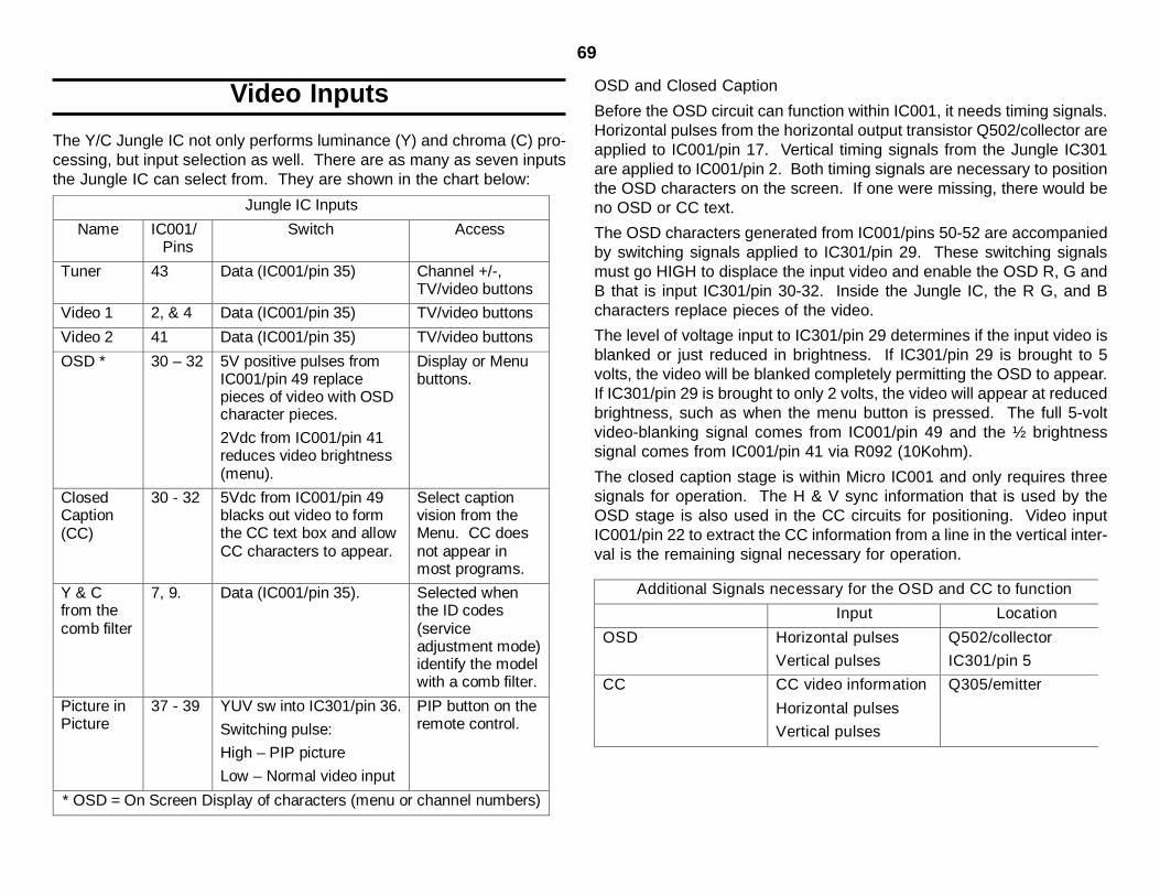
69
Video Inputs
The Y/C Jungle IC not only performs luminance (Y) and chroma (C) pro-cessing, but input selection as well. There are as many as seven inputsthe Jungle IC can select from. They are shown in the chart below:
Jungle IC Inputs
Name IC001/Pins
Switch Access
Tuner 43 Data (IC001/pin 35) Channel +/-,TV/video buttons
Video 1 2, & 4 Data (IC001/pin 35) TV/video buttons
Video 2 41 Data (IC001/pin 35) TV/video buttons
OSD * 30 – 32 5V positive pulses fromIC001/pin 49 replacepieces of video with OSDcharacter pieces.
2Vdc from IC001/pin 41reduces video brightness(menu).
Display or Menubuttons.
ClosedCaption(CC)
30 - 32 5Vdc from IC001/pin 49blacks out video to formthe CC text box and allowCC characters to appear.
Select captionvision from theMenu. CC doesnot appear inmost programs.
Y & Cfrom thecomb filter
7, 9. Data (IC001/pin 35). Selected whenthe ID codes(serviceadjustment mode)identify the modelwith a comb filter.
Picture inPicture
37 - 39 YUV sw into IC301/pin 36.
Switching pulse:
High – PIP picture
Low – Normal video input
PIP button on theremote control.
* OSD = On Screen Display of characters (menu or channel numbers)
OSD and Closed Caption
Before the OSD circuit can function within IC001, it needs timing signals.Horizontal pulses from the horizontal output transistor Q502/collector areapplied to IC001/pin 17. Vertical timing signals from the Jungle IC301are applied to IC001/pin 2. Both timing signals are necessary to positionthe OSD characters on the screen. If one were missing, there would beno OSD or CC text.
The OSD characters generated from IC001/pins 50-52 are accompaniedby switching signals applied to IC301/pin 29. These switching signalsmust go HIGH to displace the input video and enable the OSD R, G andB that is input IC301/pin 30-32. Inside the Jungle IC, the R G, and Bcharacters replace pieces of the video.
The level of voltage input to IC301/pin 29 determines if the input video isblanked or just reduced in brightness. If IC301/pin 29 is brought to 5volts, the video will be blanked completely permitting the OSD to appear.If IC301/pin 29 is brought to only 2 volts, the video will appear at reducedbrightness, such as when the menu button is pressed. The full 5-voltvideo-blanking signal comes from IC001/pin 49 and the ½ brightnesssignal comes from IC001/pin 41 via R092 (10Kohm).
The closed caption stage is within Micro IC001 and only requires threesignals for operation. The H & V sync information that is used by theOSD stage is also used in the CC circuits for positioning. Video inputIC001/pin 22 to extract the CC information from a line in the vertical inter-val is the remaining signal necessary for operation.
Additional Signals necessary for the OSD and CC to function
Input Location
OSD Horizontal pulses
Vertical pulses
Q502/collector
IC301/pin 5
CC CC video information
Horizontal pulses
Vertical pulses
Q305/emitter
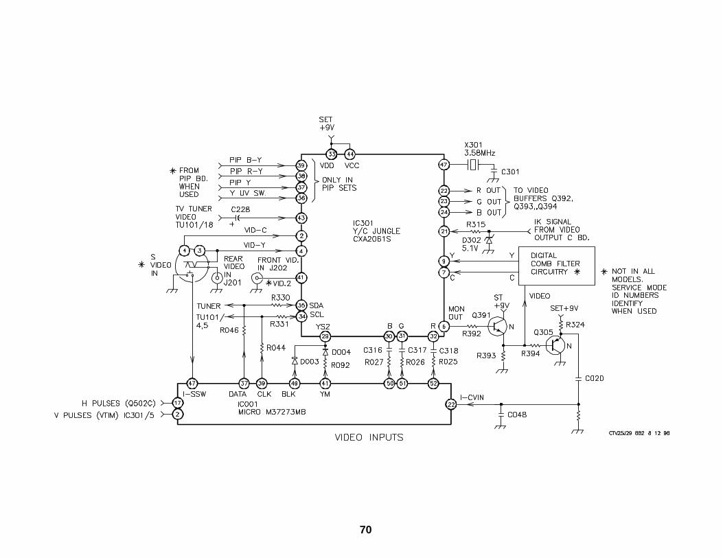
70

71
NOTES
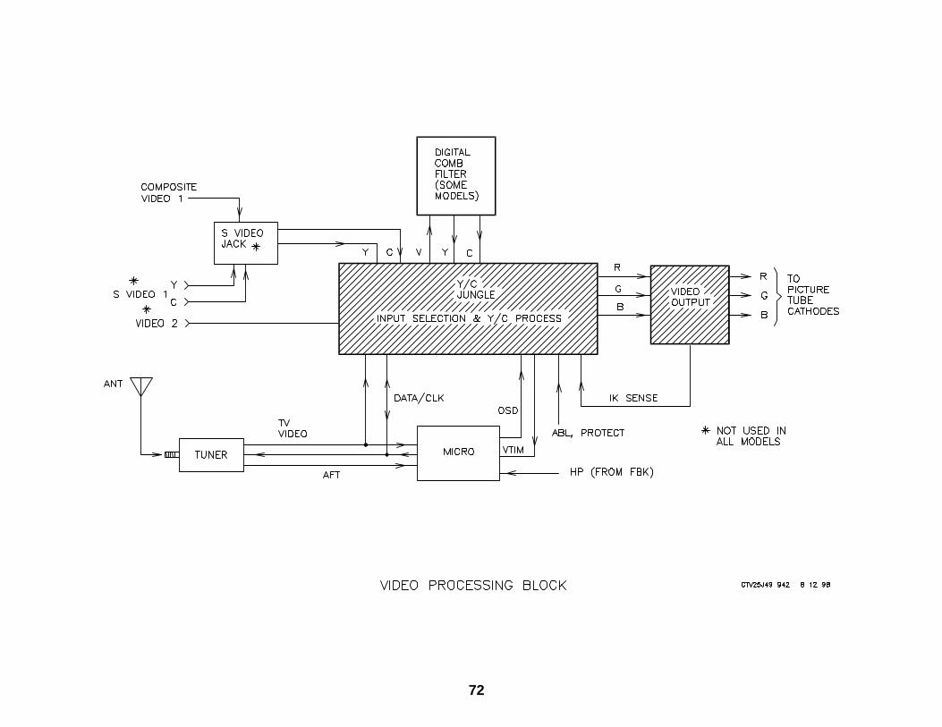
72

73
Video Output
The video output stage utilizes the parts listed below to produce andcontrol the picture:
Video Buffers
These three buffer transistors provide current drive to sink the currentfrom IC701. A short in one of these transistors would stop that color (andactivate blanking via the IK circuit). An open transistor will cause thatcolor to go to a high brightness (with retrace lines).
CRT Amplifier
This IC package amplifies the RGB signal from the buffers to a sufficientvoltage to drive the cathodes of the picture tube.
Cathode Current Adjusting (IK) CircuitConcept
As the picture tube ages, the electron output of the three cathode struc-tures will no longer be the same. The cathode current (IK) circuit moni-tors the current of each cathode and adjusts the electronic drive signallevel to compensate for the differences due to aging. As the tube isbeing used, normal wear causes the cathodes to decrease in output atdifferent rates. When one cathode has dropped in output below theothers, white color no longer appears white. White balance is now “off”.Increasing one of the R, G or B drive signal levels to the deficient cath-ode increases that cathode’s electron emission so its output will be likethe others. The picture quality can be automatically maintained with thiscircuit.
Circuitry
The automatic cathode current adjusting circuit keeps the video and OSDblanked until the AKB circuit has finished. The Y/C Jungle IC301 gener-ates the cathode drive pulse to begin the IK circuit operation. Threehorizontal lines in the vertical interval of the field above the picture areused to test each cathode, one at a time. Each cathode is driven fullON, starting with the Red output at pin 22. After the first pulse at pin 22,IC301/pin 23 sends a 10usec pulse to turn on the green cathode for theentire horizontal line. After the pulse at IC301/pin 23 returns LOW, pin24 outputs the last pulse to turn on the blue cathode. These 10usec.width positive drive pulses are buffered by Q392-Q394 and amplified byIC701 to be applied to the picture tube cathodes.
F i n a l P a r t s i n t h e V i d e o O u t p u t S t a g e
P a r t L o c a t i o n P u r p o s e
Y / C J u n g l eI C 3 0 1
M a i n A b o a r d S e p a r a t e s v i d e o i n t o Y & Cc o m p o n e n t s w h e n t h e r e i s n oe x t e r n a l c o m b f i l t e r .
U s e s t h e Y ( B & W ) s i g n a l t o a d j u s tt h e R G B o u t p u t v o l t a g e l e v e l .
S e p a r a t e s t h e C i n p u t i n t o R G Bv o l t a g e s .
A d j u s t s R G B d r i v e l e v e l s t om a i n t a i n p r e s e t c a t h o d e c u r r e n t .R e q . I K f e e d b a c k s i g n a l .
C R T A m p I C 7 0 1 C b o a r d A m p l i f i e s t h e R G B d r i v e s i g n a l
P ic t u r e t u b e F r o n t c a b i n e tb e z e l
P r o d u c e a c o l o r p i c t u r e .
Video signal PathY/C Jungle IC301
Within Y/C Jungle IC301, the input signal is selected, processed andconverted to RGB. The RGB signal undergoes some final processingbefore leaving the Jungle IC301.
L a t e r P r o c e s s i n g I n t e r n a l t o I C 3 0 1
P r o c e s s i n gS t a g e
O p e r a t i o n P u r p o s e
O S D M i x e r T h e O S D c h a r a c t e r s r e p l a c et h e R G B s i g n a l .
I n s e r t O S D o r C Cc h a r a c t e r s i n t o t h ep i c t u r e .
B l a n k i n g U s e s A B L s i g n a l f r o m t h eF B T t o r e d u c e R G B d r i v ev o l t a g e .
B l a n k ( g n d ) t h e R G B O u t p u ts i g n a l a n d i n s t r u c t s I C 0 0 1 t os h u t o f f t h e T V i f t h e r e i s ag r o u n d a t I C 3 0 1 / p i n 1 8 .
U s e s F B T h i g hv o l t a g e t o l im i t t h eb r i g h t n e s s o f t h ep i c t u r e .
E x c e s s i v e F B Tv o l t a g e o r B + c u r r e n tw i l l c a u s e I C 3 0 1 / p i n1 8 t o b e g r o u n d e d .I C 3 0 1 i n f o r m s I C 0 0 1t o p r o t e c t t h e T V b yt u r n i n g t h e T V O F F .
G a i n C o n t r o l T h e g a i n a n d l e v e l o f t h eR G B s i g n a l s i s s e t b y I 2 Cc o m m u n ic a t i o n s d a t a ( S D A )b e f o r e o u t p u t . P i c t u r e t u b ec a t h o d e c u r r e n t ( I K )f e e d b a c k i s u s e d t o m a i n t a i nR G B l e v e l s .
M a i n t a i n s g o o d w h i t eb a l a n c e .

74

75
When the picture tube warms up and draws current, these three pulsesall appear next to each other at the common cathode IK pin 5 of IC701.The amplitudes represent the current of each cathode.
Clipper Stage – Q301, Q302.
This IK signal is applied to a signal clipper stage to cut off low and highlevel parts of the waveform. The clipper circuit consists of a voltage di-vider and two transistors. The voltage divider resistors R321 and R322place the base of both transistors at a threshold voltage. The IK signal isapplied to both transistors’ emitters. When the IK signal rises above thisthreshold, both transistors conduct and pass only the signal above thisvoltage threshold. Therefore this stage is said to clip the lower voltagecomponents of the positive IK signal, leaving the just the peaks.
In normal operation, the IK line consists of the three IK pulses and thevideo signal from the picture tube cathodes. Q301 passes the signal tothe Y/C Jungle IC301 so the IK pulses can be identified and used forcathode current balancing. Zener D301 limits the signal input to the Y/CJungle IC301/pin 21 to a 5-volt maximum pulse.
Q302 is used to clip the larger amplitude signals. Q302 operates similarlyto Q301, but passes the IK signal to ground, dividing the signal current.As the signal amplitude becomes larger, more current flows through R329.The additional voltage dropped by R329 turns Q302 ON harder than Q301.As Q302 turns ON harder, the level of the video signal (or any other volt-age spike from the picture tube) is reduced so it does not damage the Y/C Jungle IC301.
The following waveforms show the IK signal entering the signal clipperstage (CH 1) and the signal leaving (CH 2). Note that only the top half ofthe IK waveform is allowed to pass.
Color bar pattern on TV screen. Digital scope is set for peak waveformpresentation. The 3 IK pulses are difficult to see in this digital picture, butare present to the right of the open (vertical) area. The vertical lines in thewaveform represent the horizontal scan lines.
Channel 1 – CN301/pin 4; 2v/div.
Channel 2 – D301/Cathode; 1V/div.
Time base = 2msec/div.
The output IK signal is applied to IC301/pin 21. Inside IC301, each one ofthe three IK pulses is measured and compared to technician set levelsstored in memory. These levels stored in memory are accessed from theservice mode (see the service manual). The information is adjusted andused to set the gain of the RGB signals. When the gain is within theautomatic adjustment range, the RGB signal is unblanked and leavesIC301 (pins 22-24) with the IK pulses.
CH 1
CH 2
T ra n s is t o r V o lta g e s – C o lo r B a r T e s t P a t te rn
T ra n s is t o r E m it te r B a s e C o ll e c to r
Q 3 9 2 0 1 .5 V d c 2 .2 V d c
Q 3 9 3 0 1 .5 V d c 2 .1 V d c
Q 3 9 4 0 1 .6 V d c 2 .2 V d c
Q 3 0 0 0 0 .4 6 V d c 3 .4 V d c
Q 3 0 1 3 .8 V d c 3 .7 3 V d c 0 .7 8 V d c
Q 3 0 2 3 .9 V d c 3 .7 3 V d c 0
Spot Elimination CircuitSince many cable boxes shut off power by removing AC when the TV isON, the TV could leave a spot of light at the center of the picture tube.This is because the TV’s magnetic deflection would collapse first beingthe most power hungry, leaving residual beam current to produce a cen-ter spot.
Q701, D700, D702, and D703 will drive the CRT harder depleting thebeam current when AC is lost. Normally with the TV ON, Q701 is turnedON with bias from B+ via zener D700. Q700’s collector voltage is LOW.When AC vanishes, B+ is lost and Q700”s collector voltage rises to applySet +9Vdc to IC701/pins 1&2 (via diodes). This drives the blue andgreen beams full ON before deflection ceases, depleting the power pro-viding beam current. The reduced beam current eliminates the possibilityhaving a spot on the screen.

76
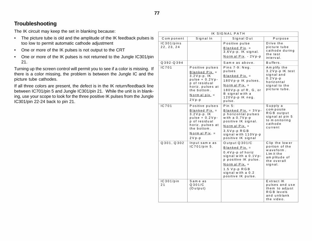
77
TroubleshootingThe IK circuit may keep the set in blanking because:
• The picture tube is old and the amplitude of the IK feedback pulses istoo low to permit automatic cathode adjustment
• One or more of the IK pulses is not output to the CRT
• One or more of the IK pulses is not returned to the Jungle IC301/pin21.
Turning up the screen control will permit you to see if a color is missing. Ifthere is a color missing, the problem is between the Jungle IC and thepicture tube cathodes.
If all three colors are present, the defect is in the IK return/feedback linebetween IC701/pin 5 and Jungle IC301/pin 21. While the unit is in blank-ing, use your scope to look for the three positive IK pulses from the JungleIC301/pin 22-24 back to pin 21.
IK S IG N A L P A T H
C o m p o n e n t S ig n a l In S ig n a l O u t P u rp o s e
IC 3 0 1 /p in s2 2 , 2 3 , 2 4
P o s it iv e p u ls e
B la n k e d P ix . =3 .6 V p -p . IK s ig n a l.
N o rm a l P ix . - 2 V p -p
D r iv e th ep ic tu re t u b ec a t h o d e d u r in gth e te s tin te rv a l.
Q 3 9 2 -Q 3 9 4 S a m e a s a b o v e . B u ffe rs .
IC 7 0 1 P o s it iv e p u ls e s
B la n k e d P ix . =3 .2 V p -p . IKp u ls e + 0 .2 V p -p o f r e s id u a lh o r iz . p u ls e s a tth e b o t to m .
N o rm a l p ix . =
2 V p -p
P in s 7 -9 : N e g .p u ls e s
B la n k e d P ix . =
1 8 0 V p -p IK p u ls e s .
N o rm a l P ix . =
1 8 0 V p -p o f R , G , o rB s ig n a l w ith a1 2 0 V p -p IK n e g .p u ls e .
A m p li fy t h e3 .2 V p -p IK te s ts ig n a l a n d0 .2 V p -ph o r iz o n t a ls ig n a l to th ep ic tu re t u b e .
IC 7 0 1 P o s it iv e p u ls e s
B la n k e d P ix . =3 .2 V p -p . IKp u ls e + 0 .2 V p -p o f r e s id u a lh o r iz . p u ls e s a tth e b o t to m .
N o rm a l P ix . =
2 V p -p
P in 5 :
B la n k e d P ix . = 3 V p -p h o r iz o n ta l p u ls e sw it h a 0 . 7 V p -pp o s it iv e IK s ig n a l.
N o rm a l P ix . =
3 .5 V p -p R G Bs ig n a l w ith 1 1 0 V p -pp o s it iv e IK s ig n a l
S u p p ly ac o m p o s i teR G B o u t p u ts ig n a l a t p in 5to m o n ito r in gc a t h o d ec u r re n t
Q 3 0 1 , Q 3 0 2 In p u t s a m e a sIC 7 0 1 /p in 5 .
O u tp u t Q 3 0 1 / C
B la n k e d P ix . =
0 .4 V p -p o f h o r izs ig n a l w ith a 0 .1 V p -p p o s it iv e IK p u ls e .
N o rm a l P ix . =
1 .5 V p -p R G Bs ig n a l w ith a 0 .2p o s it iv e IK p u ls e .
C lip th e lo w e rp o r t io n o f th ew a v e fo rm .L im it th ea m p litu d e o fth e o v e r a l ls ig n a l.
IC 3 0 1 /p in2 1
S a m e a sQ 3 0 1 /C(O u tp u t )
E x t ra c t IKp u ls e s a n d u s eth e m to a d ju s tR G B le v e lsa n d u n b la n kth e v id e o .

78

79
Video Block – 27 with PIP
An A/V switch to accommodate the second tuner and the Picture in Pic-ture (PIP) board are the only sections have been added into the 27” BA-4 chassis. The video signal flow is the same as in the 20” BA-4 chassis.
A/V Switcher Inputs / Outputs
Inputs Outputs
Tuner 1 V 1 is the main picture video tothe Jungle IC.
Tuner 2 (optional) V 2 is the video signal to the PIPboard.
Video 1 (Composite or S Video)
Video 2 (optional)
Video 3 (optional)
Picture in Picture (PIP) Board Signal Flow
PIP Board Input / Outputs
Input Output
Video 1 from the A/V switcher IC Luminance (Y),
R-Y (V), and
B-Y (U).
PIP insertion signal (YUV)
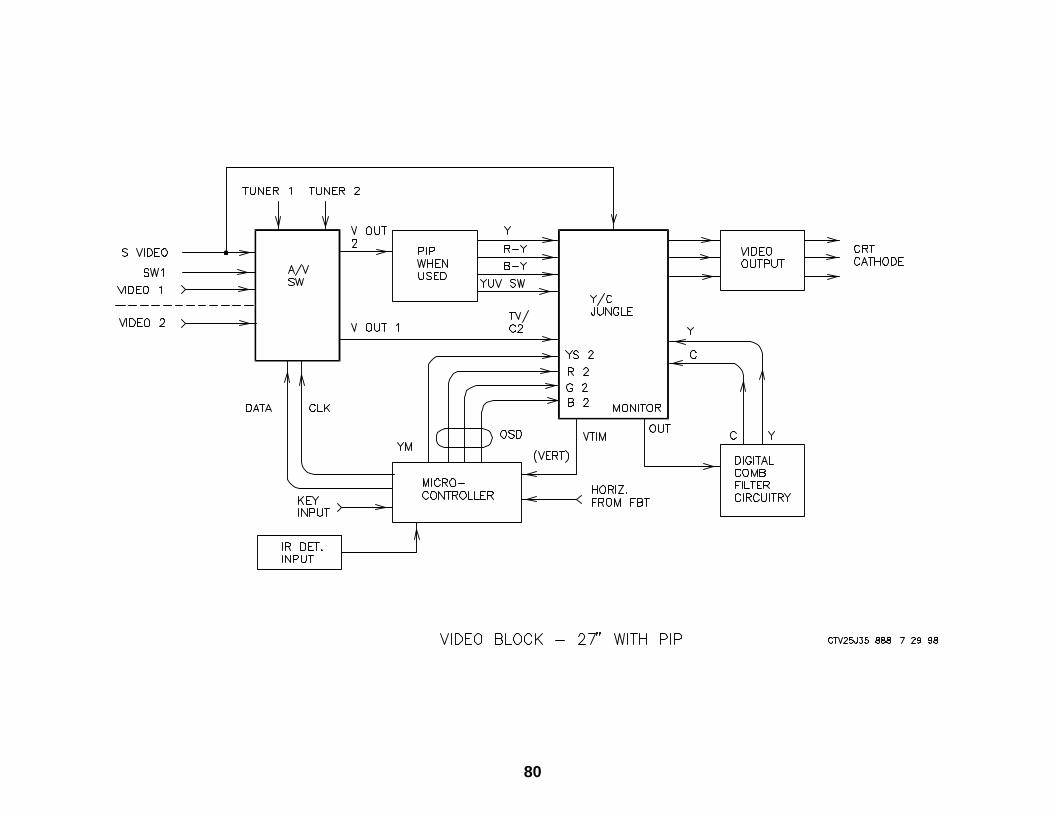
80

81
Picture In Picture ProcessingOverviewThe purpose of the Picture in Picture circuitry on the small P board is todigitally compress the normal 525 line transmitted picture into a smallpicture 1/9 its original size. To do this, the PIP processor IC must firsttake the analog luminance and color information and convert it to digitalformat. Then, using the vertical and horizontal sync pulses, this IC elimi-nates information, which makes the picture smaller. The remaining infor-mation is then stored into memory. When PIP is called for by the cus-tomer, the memory picture is converted from digital back to analog be-fore leaving the PIP Processor IC3303/pins 7-9 as Y, R-Y (V), and B-Y (U).
PIP IC Operations
IC Purpose
ChromaDecoderIC3304
Converts incoming video to Y, V, and U.
Alters outgoing V & U signals to match the mainpix color using SCP (video) from Jungle IC301.
PIPProcessorIC3303
Uses H & V to make the pix smaller.
Stores the child pix into memory.
Analog to Digital for memory storage andreverse to PB.
Most of this child picture processing is done in IC3303, which makestroubleshooting simpler. The other main IC is a chroma decoder, IC3304,that converts the incoming video into Y, R-Y and B-Y for the PIP Proces-sor IC3303.
ProcessingThe Picture in Picture circuit board needs the following signals to oper-ate. These signals are present all the time when the set is ON, whetherthe Picture in Picture section is being turned on or not. These signalsare:
1) Serial data and clock signal at connector CN302/12 and 13.2) +9V at CN302/1, which becomes +5Vdc on the board.3) Input video signal at CN302/2 = 2Vp-p.4) The P board uses the child pictures sync to sample and store the
child picture. The main picture’s vertical and horizontal pulses areused to determine where the beam is at any given moment, so thePicture in Picture can be output for main picture insertion at the properlocation. These input timing signals are approximately 5Vp-p.
The Y, R-Y and B-Y signals that leave the P board when PIP is turnedON have to be switched into the main picture at the correct time. That isthe purpose of the YUV (or PYS in several other sets) signal that is out-put at pin 17 when the child picture is simultaneously output. This YUVsignal to Jungle IC301/36 selects the main picture when LOW and thePicture in Picture when HIGH. Conceptionally, the YUV signal cuts ahole in the picture in which the child picture is inserted.
When Picture in Picture is called for from the remote control, all fourPicture in Picture inputs to the Jungle IC301/ 9, 10, 11 and 12 will beactive.
Signal FlowThe video or child picture that enters the Picture in Picture board at CN302/pin 2 is a 2Vp-p video signal that is input to the Chroma Decoder IC3304.IC3304 outputs the video as Y, R-Y and B-Y labeled as Y, V and U atIC3304/18, 19 and 20. (The simpler labeling of Y, V and U in place of Y,R-Y and B-Y has been used in Europe for years.)
The Picture in Picture processor IC3303 outputs child picture informationwhen serial data (SDA, SCL) is input and calls for that feature. At thattime, only when PIP is turned ON does the child picture information out-put from IC3303’s Y, V and U output terminals.

82

83
Deflection Block
There are several sections to a TV’s main horizontal and vertical Deflec-tion stage:
Deflection SectionsName Sections Purpose
HorizontalOutput
Y/C JungleDriveOutput
Horiz. oscillator.Horiz. amplifier.Horiz. amplifier to drive the horizontaldeflection yoke.
Pincushion Y/C Jungle (E/W =east/west) PincushionAmp
Hourglass shaped pictures occur inyoke deflection angles 100o or more.This stage increases width at left andright sides to compensate.
High Voltage Horiz. OutputFlyback Transformer(FBT)
Makes primary drive signal.Develops picture tube accelerating highvoltage.Makes remainder of tube and verticaloutput voltages.
Horiz (HP)AFC /Protection
Horiz OutputResistive VoltageDividers, TransistorsJungle ICMicro
Compares huge horiz output pulses(HP) and video sync for AFC lock of H.oscillator.Excessive B+ current or FBT voltagesare detected by the Jungle IC. Datatransmitted to the Micro will shut OFFthe TV.
ABL FBT Limits picture brightness by using tubecurrent to reduce RGB drive.
Vertical Jungle ICVertical Output
Vertical Oscillator.Vertical Amplifier to drive thedeflection yoke.

84

85
Vertical Deflection
The vertical deflection stage consists of:
• Vertical oscillator
• Vertical amplifier
• Flyback generator
• Deflection yoke
The purpose of this stage is to manufacture a magnetic field. The mag-netic field will bring the electron beam gradually from top to bottom (ver-tically) and then quickly back to the top (beam retrace) of the screen tostart over again.
Vertical OscillatorWhen the TV is turned ON, Set +9Vdc appears at Y/C Jungle IC301/pin44. The internal horizontal oscillator begins and is counted down (di-vided) to 60 Hz to become the vertical drive signal.
The drive signal is formed into a positive and negative ramp to be changedin amplitude and linearity by the serial data from Micro IC001. If the dataor clock signal were missing, there would be NO vertical drive signaloutput IC301/pins 13 and 14.
Vertical AmplifierA single package vertical amplifier and output IC541 generates sufficientamplitude and current to drive the deflection yoke. It is powered with+13Vdc from the flyback transformer secondary.
Flyback / Boost GeneratorThe vertical waveform is used to generate extra current in the deflectionyoke during the retrace period. This extra current is used to quickly re-turn the electron beam to the top of the picture.
The flyback generator stage within IC541 uses the vertical waveform tomake a 30Vp-p pulse needed during retrace time. The retrace portion ofthe vertical drive waveform input IC541/pins 13-14 is extracted, ampli-fied and appears at pin 3 as a 30Vp-p pulse. It passes through C541 to
provide sufficient current to power IC541/pin 6 during retrace time. Di-ode D542 blocks this pulse and prevents it from increasing the +13 voltsource.
The vertical flyback signal from IC541/pin 3 is used in the protectioncircuit. This 30Vp-p signal from pin 3 is reduced to 5Vp-p and monitoredby Micro IC001 to prove the vertical stage is working.
Deflection yokeThe deflection yoke translates the electrical current flowing through itscoils into a magnetic field that positions the election beam vertically.Current flowing through the deflection yoke coil is returned to groundthrough R544. The voltage developed across this resistor is fed back tothe inverting input of IC541/pin 1 to improve linearity.
ProtectionA loss of data, vertical drive, flyback generator signal or +13Vdc powerwill cause the protection circuit to shut OFF the TV. The 30Vp-p retracepulse from IC541/pin 3 is used as an indication of vertical output opera-tion. This pulse is reduced to 5Vp-p and monitored by Micro IC001/pin17. After two seconds of missing pulses, IC001 will turn OFF the TV setand blink the Timer light four times.
TroubleshootingWhen the TV is shutdown and the Timer/Standby light blinks four times,the problem is in the vertical or horizontal section. Start the TV by press-ing the Power button. You have two seconds to identify the missingsignal with your scope or voltmeter before the TV shuts down again.Here is a general checklist of items that will cause the TV to shutdown:
Some causes for the Timer/Standby light to blink four times and repeat
S om e c au ses fo r th e T im er/S tan d b y lig h t to b lin k fou r t im es an drep e at
• N o D ata /C loc k in p u t(IC 3 0 1 /p in 3 4 , 3 5 ). T h isc au s es N O IC 3 0 1 /p in s 1 3 -1 4d rive ou tp u t .
• M iss in g p os it iv e o r n eg at ive1 3 vo ltag e to p ow e r IC 5 4 1 a tp in s 2 o r 4 . T h is vo ltag ec om es from th e F B T .
• L os s o f e ith er o r b o th vert ic a ld rive s ig n a ls from IC 3 0 1 /p in s1 3 an d /or 1 4 .
• L os s o f h oriz on t a l d riveresu lt in g in n o F B T vo ltag e s .
• N o fb t /b o os t ou tp u t fromIC 5 4 1 /p in 3
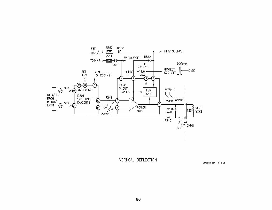
86

87
NOTES

88

89
Horizontal Deflection
The horizontal deflection stage consists of several sections:
• Horizontal Oscillator• Horizontal Drive• Horizontal Output• AFC feedback• Automatic Brightness Limiting (ABL)• ProtectionHorizontal OscillatorWhen the TV is turned ON, Set +9Vdc appears and is applied to Y/CJungle IC301/pin 33. Internally, IC301’s horizontal oscillator starts andshapes this signal into a horizontal drive pulse that leaves pin 19. Thepulse is 4Vp-p with a positive width of 24usec. The waveform staysLOW for 40usec. after the pulse and repeats.
Horizontal DriveThe horizontal signal from IC301 is amplified by IC501. The signal levelsare shown in the following chart:
Horizontal DriveLocation Amplitude Vdc
IC301/pin 19 4Vp-p 3VdcQ501/base 3Vp-p 0.7VdcQ501/collector 100Vp-p 47VdcQ502/base 2Vp-p
(6Vp-p w spikes)0.03Vdc
In the KV20M40 model TV, Q501 amplifies the horizontal drive signal to100Vp-p (B+ = +116Vdc). The drive signal is reduced in voltage, butincreased in current by T501. The increased current at the secondary isnecessary to drive the low gain, higher power and horizontal output tran-sistor Q502.
Horizontal OutputQ502 is the output transistor that drives two inductive loads and twocircuits:
• The deflection yoke – Develops a magnetic field in order to move theelectron beam from left to right on the screen.
• The flyback transformer – Develops high, focus, screen and +13Voltsfor the picture tube and TV’s vertical section.
• AFC feedback circuit – Used to monitor the frequency of the horizon-tal oscillator.
AFC feedbackA sample of the horizontal output signal from Q502/collector is used tokeep the horizontal oscillator locked to the incoming video sync. Thehigh voltage pulse at Q502/collector is reduced by voltage divider C509and C508 to 23Vp-p and again by R318 and R320 to 5Vp-p. The 5Vp-psignal passes through C313 and R310 to IC301/pin 18.
Inside IC301, this horizontal output signal is compared to the incomingvideo sync and a correction voltage is developed. The correction volt-age is used to keep the frequency of the Jungle’s horizontal oscillator instep with the incoming video. This is the automatic horizontal frequencycorrection (AFC).
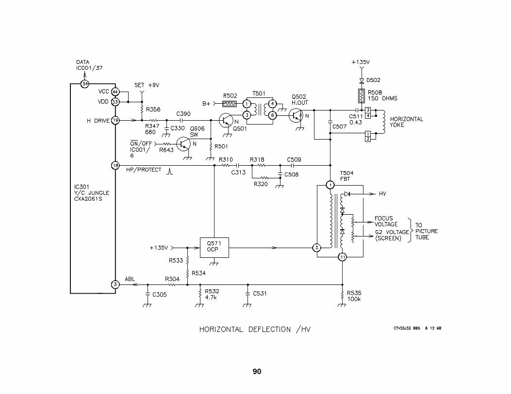
90

91
A B L V o lta g e s – M o d e l K V 2 0 M 4 0
C o n d it io n T 5 0 4 /p in 1 1 V o lta g e IC 3 0 1 /p in 3 V o lta g e
B la c k s c re e n(g e n e r a t o r)
6 .2 V d c 6 .2 V d c
C o lo r b a rs 2 .9 6 V d c 3 V d c
W h ite s c re e n 2 .1 V d c 2 .1 V d c
Voltage divider R533, R534 and R532 bias this ABL line with a positivevoltage that is applied to Jungle IC301/pin 3. A lower ABL voltage de-creases the level and gain of the RGB waveform. This is how ABL sec-tion uses the Jungle IC to keep the brightness within a reasonable oper-ating range.
OCP ProtectionOne part of the protection circuit is shown here in block form. The overcurrent Protection (OCP) stage shuts OFF the TV during a fault. Q571 isused to monitor the current flowing through the FBT and horizontal out-put transistor. If the current becomes excessive, Q571 conducts, ground-ing out the DC voltage from the Jungle IC301/pin 18. This ground causesIC301/pin 34 to send data to Micro IC001/pin 37. The data instructsIC001 to shut OFF the TV, allowing the horizontal output transistor tocool down.
Automatic Brightness Limiting (ABL)The purpose of this circuit is to prevent sudden bright scenes from short-ening the life of the picture tube. It does this automatically by monitoringthe picture tube’s current and then using this voltage to limit the bright-ness of the picture.
The flyback transformer T504 (secondary) supplies the picture tube’shigh voltage. The ground end of the secondary at T504/pin 11 is currentlimited by a 100k ohm resistor, R535. As the picture gets brighter, thehigh voltage current increases, causing a voltage drop across R535. ThisABL voltage decreases with increasing brightness.

92

93
Protection
The TV’s protection circuitry either blanks the video or turns the TV OFF.Protection can be caused by a failure in one of these stages:
Failures Activating TV ProtectionPicture Blanking (sound OK) Shutdown - TV = OFF
1. Loss of R, G, or B drives fromIC301
1. Vertical Failure - loss of boost pulsefrom IC541/pin 3).
2. Ik signal from C board missingpulses
2. Horizontal drive failure stopspowering the FBT. The FBT stopspowering vertical IC541.
3. Screen control misadjusted 3. Excessive FBT secondary voltage4. Picture tube weak 4. Excessive B+ current to FBT and/or
H. Output transistor.5. ABL voltage to IC301/pin 3
missing
The picture blanking protection was explained in the video output docu-ment of this training manual.
The remaining protection circuits shut the TV OFF. They are shown herecontrolled by Micro IC001. There are only three circuits that tell IC001 toturn OFF the TV:
Protection Circuits that turn the TV OFF
Defective Stage Trigger Mechanism IC001 Input
Vertical Output Missing vertical pulses. Loss of V pulses for 2seconds at pin 17.
FBT Output Excessive output voltage Data into pin 37
B+ Excessive current Data into pin 37
Vertical Output FailurePulses from the vertical output IC are monitored for activity by IC001.Two signals are output when the vertical output stage is receiving thedrive signal and amplifying. The main drive signal goes to the verticaldeflection yoke. The other signal is made inside the vertical Output IC541’sflyback generator and output pin 3. At pin 3 is a 30Vp-p pulse that isreduced by R549 and limited by zener diode D001 to 5Vp-p. IC001/pin17 receives and monitors this 5-volt vertical pulse to prove the Verticalstage is operating.
If IC001 detects a loss of these vertical flyback pulses for two seconds,IC001 will turn the TV OFF. As part of IC001’s diagnostic program, afterthe set is turned OFF (but not unplugged), the Timer/Standby light willblink four times, pause and repeat. This indicates the problem is a lossof vertical signal.
Unfortunately, +13Vdc that powers the vertical IC541 comes from thehorizontal stage (FBT). Therefore, a horizontal failure will also cause thelight to blink four times, pause and repeat.
Excessive FBT VoltageAn open safety capacitor C508 or high B+ voltage can cause the flybacktransformer (FBT) to produce an undesirably high secondary voltage.The FBT’s secondary voltage at T504/pin 7 is monitored for excessivesignal level.
This stage consists of T504, D574, IC521, Q300, IC301 and IC001.Flyback pulses are rectified and compared to a reference voltage to de-termine if they are excessive. The 120Vp-p T504/pin 7 pluses are recti-fied by D574 into 109.2Vdc. This voltage is reduced further to 8.76Vdcby voltage divider resistors R583, R582 and R584 and applied to the +input of comparator IC521/pin 5. As long as the voltage at pin 5 is nohigher than the 9.7Vdc at the negative input pin 6, the output of IC521/pin 7 will remain LOW (1.34Vdc).
The Jungle IC detects the comparator output. The LOW from compara-tor IC521/pin 7 is applied to Q300/base, keeping it OFF as if it were notin the circuit. This allows the horizontal pulses from Q502/collector andthe internal voltage of 3.4Vdc to remain at Jungle IC301/pin 18 for nor-mal operation.

94
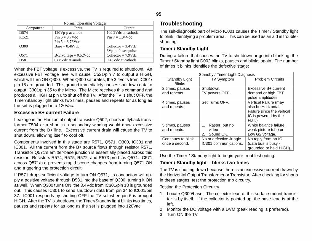
95
Normal Operating VoltagesComponent Input Output
D574 120Vp-p at anode 109.2Vdc at cathodeIC521 Pin 6 = 9.7Vdc
Pin 5 = 8.76VdcPin 7 = 1.34Vdc
Q300 Base = 0.46Vdc Collector = 3.4Vdc5Vp-p; 9usec pulse.
Q571 B-E voltage = 0.52Vdc Collector = 7.9VdcD581 0.88Vdc at anode 0.46Vdc at cathode
When the FBT voltage is excessive, the TV is required to shutdown. Anexcessive FBT voltage level will cause IC521/pin 7 to output a HIGH,which will turn ON Q300. When Q300 saturates, the 3.4volts from IC301/pin 18 are grounded. This ground immediately causes shutdown data tooutput IC301/pin 35 to the Micro. The Micro receives this command andproduces a HIGH at pin 6 to shut off the TV. After the TV is shut OFF, theTimer/Standby light blinks two times, pauses and repeats for as long asthe set is plugged into 120Vac.
Excessive B+ current FailureLeakage in the Horizontal output transistor Q502, shorts in flyback trans-former T504 or a short in a secondary winding would draw excessivecurrent from the B+ line. Excessive current drain will cause the TV toshut down, allowing itself to cool off.
Components involved in this stage are R571, Q571, Q300, IC301 andIC001. All the current from the B+ source flows through resistor R571.Transistor Q571’s emitter-base junction is essentially placed across thisresistor. Resistors R574, R575, R572, and R573 pre-bias Q571. C571across Q571/b-e prevents rapid scene changes from turning Q571 ONand triggering the protection circuit.
If R571 drops sufficient voltage to turn ON Q571, its conduction will ap-ply a positive voltage through D581 into the base of Q300, turning it ONas well. When Q300 turns ON, the 3.4Vdc from IC301/pin 18 is groundedout. This causes IC301 to send shutdown data from pin 34 to IC001/pin37. IC001 responds by shutting OFF the TV set when pin 6 is broughtHIGH. After the TV is shutdown, the Timer/Standby light blinks two times,pauses and repeats for as long as the set is plugged into 120Vac.
TroubleshootingThe self-diagnostic part of Micro IC001 causes the Timer / Standby lightto blink, identifying a problem area. This can be used as an aid in trouble-shooting.
Timer / Standby LightDuring a failure that causes the TV to shutdown or go into blanking, theTimer / Standby light D002 blinks, pauses and blinks again. The numberof times it blinks identifies the defective stage:
Standby / Timer Light DiagnosisStandby Light
BlinksTV Symptom Problem Circuits
2 times, pausesand repeats.
Shutdown.TV powers OFF.
Excessive B+ currentdemand or high FBTpulse amplitudes.
4 times, pausesand repeats.
Set Turns OFF. Vertical Failure (mayalso be HorizontalFailure since the verticalIC is powered by theFBT.)
5 times, pausesand repeats.
1. Raster, but novideo
2. Sound OK.
White balance failure,weak picture tube orLow G2 voltage.
Continues to blinkonce a second.
No or defective JungleIC301 communications.
No reply from an IC(data bus is busy -grounded or held HIGH).
Use the Timer / Standby light to begin your troubleshooting.
Timer / Standby light – blinks two timesThe TV is shutting down because there is an excessive current drawn bythe Horizontal Output Transformer or Transistor. After checking for shortsin these stages, test the protection trip circuitry.
Testing the Protection Circuitry
1. Locate Q300/base. The collector lead of this surface mount transis-tor is by itself. If the collector is pointed up, the base lead is at theleft.
2. Monitor the DC voltage with a DVM (peak reading is preferred).3. Turn ON the TV.

96
97
4. The normal voltage should be less than 0.5Vdc. If it is less than0.5Vdc before the TV turns OFF again, there is a problem in theprotection circuit at Q300 or IC301.Test Q300 for leakage or replace.Move your DVM probe to IC301/pin 18 and turn ON the TV. If thisvoltage stays below 2Vdc, Q300 is leaky. If above 2Vdc, IC301 maybe defective.
5. If the voltage at Q300’s base is HIGHER than 0.5Vdc, the problemmay be in IC521, Q571, or in the circuitry.
6. Place your DVM at IC521/pin 7 and turn ON the TV. The normalvoltage should be less than 2Vdc. If it is higher, the problem is aroundIC521 or there is excessive FBT voltage from an open safety capaci-tor (C508) or high B+ voltage.Reduce the AC voltage and monitor the voltages at IC521/pins 5 &6. The voltage at IC521/pin 6 is fixed at the D573 zener voltageplus 0.6V (D572). The normal voltage at pin 5 should never ex-ceed 10Vdc.If the voltage at IC521/pin 5 is HIGHER than 10Vdc, the problem is inthe circuit’s safety capacitor or high B+ voltage.If the voltage at IC521/pin 5 is Lower than 10Vdc, the problem isabout IC521.
7. If none of the voltages around IC521 were high, the problem must bearound Q571, a defective horizontal output transistor or transformer.
8. Place your DVM at Q571/collector. Turn the TV ON. This voltageshould not rise above 10Vdc.If this voltage is HIGH, suspect Q571, R571 and other resistors in thearea.If these protection parts test OK, there is a heavy current demand onthe B+ line. The problem may be a short at the FBT secondary wind-ings.
Timer / Standby light – blinks four timesA vertical deflection failure or horizontal drive failure is indicated.
1. Test the horizontal section by using one of these tricks:• Place your scope probe by the FBT and turn ON the TV. You will
see the horizontal signal if the drive path from the Jungle IC tothe FBT is OK
• Listening to the frying sound at the yoke is another indicator ofhorizontal signal arriving at the yoke
2. Test the vertical stage by using the scope probe to monitor the verti-cal drive signal and the DVM to measure the positive and negativesupply voltages to the vertical IC541 at turn ON.
3. Test the Protection circuitry by placing your scope lead at the VerticalOutput IC541/pin 3. You should see a 30Vp-p pulse there. If it ispresent, this pulse is not getting to IC001/pin 17. Replace zenerD001 if shorted.
Timer / Standby light – blinks five timesThis failure is caused by a problem in the video output IK circuit. Turningup the screen control will let you see light on the screen so you can makean evaluation of the problem. For more details see the Video Outputsection of this training manual.

98
99
Self DiagnosticSelf-Diagnostic is new in the series BA-4 TV chassis. It uses a blinkinglight or OSD to notify you if there is a failure caused by the following:1. Excessive flyback current or amplitude;2. No Vertical sweep; or3. No green automatic white balancing signal.
Timer / Standby LightThe number of times the Timer/Standby light blinks indicates what failureis detected by the Control Tuning System Microprocessor IC001. IC001will shut off or blank the TV set to protect itself. The Standby/Timer lightwill continue to blink as long as the TV is plugged into AC power.
Standby / Timer Light DiagnosisStandby Light Blinks Symptom Problem2 times, pauses andrepeats.
Shutdown.TV powers OFF.
1. Excessive B+ currentdemand or high FBT pulseamplitudes.
2. No reply from JungleIC301.
4 times, pauses andrepeats.
Set Turns OFF. Vertical Failure (may also beHorizontal Failure since thevertical IC is powered by theFBT.)
5 times, pauses andrepeats.
1. Raster, but novideo
2. Sound OK.
White balance failure, weakpicture tube or Low G2 voltage.
Continues to blinkonce a second.
No or defectiveJungle IC301communications.
No reply from an IC (data busis busy, grounded or heldHIGH).
The number of times the TV has failed is held in memory. As long asthere is failure information present, the standby light will blink when theset is tuned OFF. Unplugging the TV set will clear the memory informa-
Self-Diagnostic On Screen DisplayA dormant intermittent problem is difficult to detect. The BA-4 chassisControl Tuning System IC001 has a program to record the number oftimes the TV has failed in the first three categories listed above. Thisinformation can be accessed and displayed on the TV screen as long asthe set remains plugged in.
Self-Diagnostic AccessWith the set OFF, aim the remote at the TV and press the following re-mote buttons in this sequence:1. Display2. 53. Volume Down -4. Power On
The TV will power ON and display the self-diagnostic page. This self-diagnostic display will overlay the TV or video picture.At the left of the self-diagnostic TV screen display are the numbers 2, 4and 5. These represent the number of times the Timer/Standby light wasblinking. The numbers 3 and 101 are not used (N/A).The column on the right side shows the number of failures that haveoccurred since the program was reset. Up to 99 failures can be recorded.Although the self-diagnostic page will display the number of times a fail-ure has occurred, it will not be able to tell you exactly where the problemis, only that it exists.
tion and stop the blinking.

100

101
Failure ChecklistTimes StandbyLight Blinks
Possible defect
2(Excessive currentor FBT amplitude)
1. Horizontal Output Transistor leaky/shorted.2. Flyback shorted.3. Flyback secondary load is shorted.4. Safety/resonate capacitor opens (C508 in this set).5. Sensing circuit defect (IC521, Q571 and Q300).6. No reply from Jungle IC301.
4(Vertical failure)
1. Vertical Output IC541 failure.2. Open R549/open foil path.3. Shorted D549.4. IC001 damaged by open D001.5. No vertical drive from IC301/pin 13 and 14.6. No vertical IC541 +13Vdc power from FBT (horiz
drive failure).5(Loss of green IKsignal toIC301/pin 21)
• Green buffer transistor Q393 open or shorted.• Protection diode D706 shorted.• CRT amp IC701 defective.• Picture tube socket not making contact.• IK amplitude limiter Q302 or zener D302 damaged by
picture tube arcing.Once a second Jungle IC communications failure.
When the problem is intermittent, you will have to probe further by moni-toring the horizontal output transistor temperature and the TV’s currentconsumption to see if it is high, vibrate and possibly “bake” the set toforce the intermittent failure to reveal itself.
Memory Clear :Unplugging the TV from AC power resets the stored failure informationand stops the blinking light. The memory is cleared once standby +5Vdcis removed from the Control Tuning System Microprocessor IC001. Itcan also be manually cleared by first pressing 8 and then pressing EN-TER while you are in the self-diagnostic mode.
Clearing the Self-Diagnostic MemoryMethod Steps
A. Unplug the TV from AC. Removing AC power clears thememory at any time.
B. From the remote control. Press buttons:8, then press ENTER.
Self Diagnostic Exit:Shutting off power to the set retains the memory information and allowsyou to return to the TV picture.
Self Diagnostic CircuitThe self-diagnostic program is contained in the Control Tuning SystemIC001. The number of problems is detected by the program is stored inIC001. This number remains in IC001’s resident memory as long as theTV remains plugged into AC and is not manually cleared.
InputsWhen the TV set is turned ON, IC001 monitors three TV conditions usingtwo inputs at pins 37 and 17. These TV conditions are:1. Vertical Failure - In normal operation, Vertical Output IC541’s “Ref”
pin 3 outputs a 30Vp-p pulse (1msec pulse width). This voltage isreduced by R549 and clamped to no higher than 5Vp-p by D001.These vertical pulses from IC541/pin 3 are monitored by Control Tun-ing System IC001 at pin 17.A vertical drive failure causes no pulses to be generated. If thesevertical pulses are lost for two seconds, IC001 will turn OFF the TV toprevent the vertical deflection failure from damaging the CRT. How-ever, the front panel Timer/Standby light continues to blink four times,pauses and repeats, even though the set is OFF.
2. Excessive Current Demand/Excessive FBT pulse amplitude – Y/CJungle IC301 monitors both of these conditions at input pin 18. Nor-mally there are horizontal pulses applied to IC301/pin 18 when theTV is ON.When there is excessive current being drawn by the FBT or Horizon-tal Output Transistor, the horizontal pulses are grounded out. The Y/C Jungle IC301 detects this loss from pin 18 almost immediately andsends data from IC301/pin 35 to IC001/pin 37 (even in normal opera-tion, there is always data on this line). IC001 shuts OFF the TV to
Some of the reasons for the failure could be in this checklist.
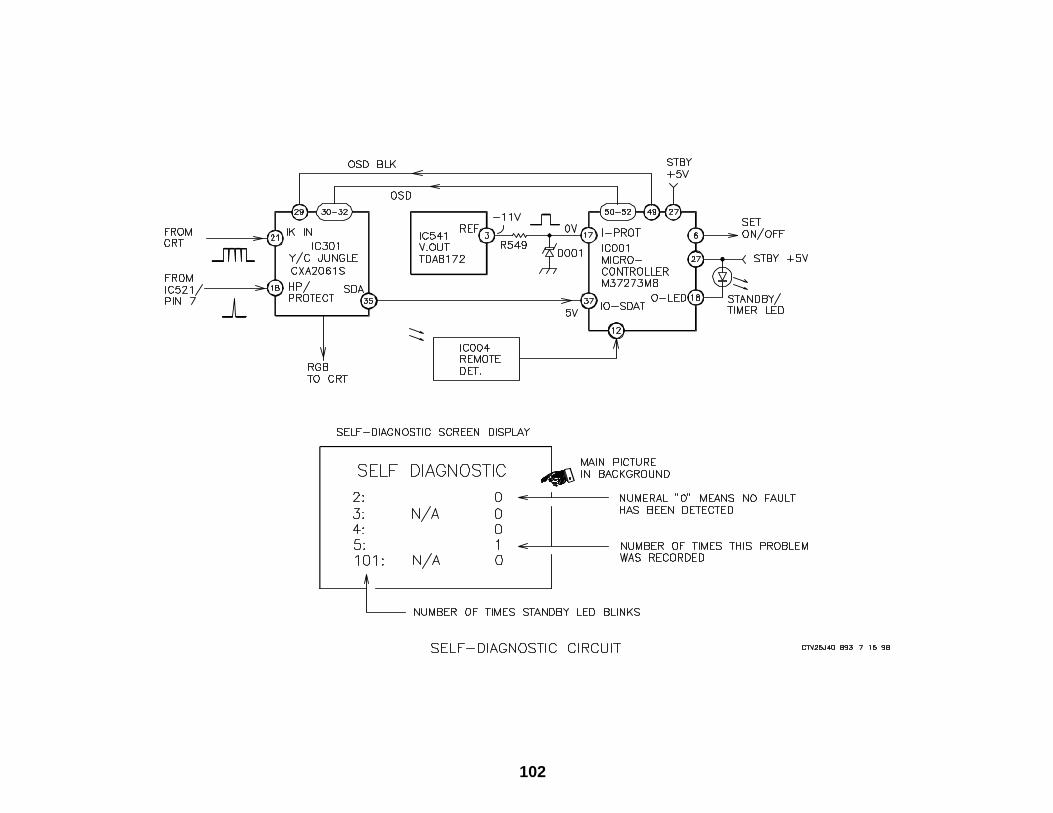
102

103
protect itself. The Timer/Standby light blinks two times, pauses andrepeats to indicate the failure.If flyback (FBT) pulses were abnormally high, perhaps as a result ofan open resonate capacitor (C508 in this set), the TV would similarlyshut down. Higher than normal FBT pulses result in a high DC volt-age that also grounds the horizontal pulses at IC301/pin 18. Theloss of horizontal pulses is detected and data is sent from IC301/pin35 to IC001/pin 37 for the TV to shut OFF. The Timer/Standby lightcontinues to blink two times, pauses and repeats after the failure.
3. White Balance Failure – Jungle IC301 initiates CRT drive and moni-tors CRT cathode current at pin 21. The amplitude of the three IKpulses that return to IC301/pin 21 represent the level of red, greenand blue CRT cathode emissions. Their amplitudes are used to whitebalance the picture while the TV is ON.This IK circuit is designed to look for three IK pulses returned fromthe picture tube. If IC301 detects a missing IK pulse within two sec-onds after the set is turned ON, the video is blanked (muted). Thetwo seconds allow time for the picture tube to warm up.This blanking state is relayed as data from IC301/pin 35 to IC001/pin37. IC001 causes the Timer/Standby light to blink five times, pauseand repeat. The set remains ON during this video failure, so thesound is still present.
When there are multiple failures, the two blinking light failure has a higherpriority over the four blinking light failure. By the same logic, the fourblinking light failure has a greater priority than the five blinking light fail-ure. For example, if multiple failures caused all of the two, four and fiveblinking light failures to be stored in memory, the Timer/Standby lightwould blink two times, pause and repeat when the TV shut down. Thenumber of failures has nothing to do with how many times the light blinks.DisplayBy using the TV’s remote control, you can access this failure informationstored in memory. Once IC001 receives the self-diagnostic access com-mand at pin 12, IC001 powers ON the TV. The failure information fromIC001 is sent to the Jungle IC301 as On Screen Display (OSD) videolevels.A “OSD Blk” signal accompanies the OSD video levels from IC001 intoIC301. This analog input voltage at Jungle IC301/pin 29 is used to darken(blank) the main RGB picture signal at the instant the OSD character is
to appear and enable the OSD. Since IC301/pin 29 is an analog input,0Vdc input leaves the main picture at normal brightness. 2Vdc inputreduces the picture to half brightness and 5Vdc blanks or mutes thepicture.
Main Picture Brightness Control with OSDVoltage at IC301/pin 29 Brightness level
0 Vdc Normal2Vdc Reduced to half5Vdc Dark – main picture muted.
The following waveform was taken with the self-diagnostic page displayedon the TV. The waveform shows that the YM/OSD BLK signal is at anaverage level of 2.0 volts for the main picture brightness reduction. Thereare peaks of the YM/OSD BLK signal that rise to 5Vdc to mute the mainpicture. These peaks correspond to the self-diagnostic OSD characters.By muting the main picture at this time, the OSD letters appear on the TVscreen without interference from the main picture.
CH 1
CH 2
Channel 1 =IC301/pin 29 – OSD Blk signal. 2V/div.Channel 2 =IC301/pin 31 – OSD green signal input. 0.5V/div.Time base = 2msec/div.
While the main picture is at half brightness, the OSD self-diagnostic pageis displayed at normal brightness and appears as an overlay to the mainpicture.

104