southeast asia - global smt & packaging magazine...into an agreement with dover printing &...
TRANSCRIPT

PLUS: ControLLing SoLder PaSte volume • Paste in Hole Printing • tHe PHysics of failure & more
SoLder PaSte jet Printing—a 3d SoLUtion
Covering india, thailand, Malaysia, singapore, the Philippines and Hong Kong
volume 5, number 1 January/february 2014
www.globalsmtsea.com
Southeast AsiaSoutheast Asia
Zoltàn Sopsitsinterview inside

www.vitechnology.com
Revolutionary
See your process like never before
Paste Inspection
Actual image from PI
Global SMT & Packaging Southeast Asia – January/February 2014 – 1www.globalsmtsea.com
Title
Friction on solder paste with 45° and 60° angles
Paste embedded by red area
Solder paste is in contact with the stencil and the squeegee blade druing the print stroke. Friction is proportional to the area. 45-degree blade holder has a larger area in contact with the solder paste. Impacts solder paste rolling Paste can stick to the blade
when the squeegee is lifted for the reverse stroke
Pure process start up condition, e.g., squeegee speed, might have to be reduced
45-degree blade holder carries process startup risk!
Global SMT & Packagingis distributed by controlled circulation to qualified personnel. For all others, subscriptions are available at a cost of €270 for the current volume (twelve issues).
No part of this publication may be reproduced, stored in a retrieval system, transmitted in any form or by any means electronic, mechanical, photocopying, recording or otherwise without prior written consent of the publisher. No responsibility is accepted for the accuracy of information contained in the text, illustrations or advertisements. The opinions expressed in the articles are not necessarily those of the editors or publisher.
ISSN No. 1474-0893© Trafalgar Publications Ltd
Designed and Published byTrafalgar Publications Ltd,London, UK
DownloAD ThiS iSSue To your Mobile Phone:
Visit www.globalsmtsea.com for the latest news and more, every day.
If you don’t already have one, search for a QR code reader app in your smartphone’s app marketplace. Then use it to scan the code above & download this magazine issue right to your phone.
Volume 5, No. 1
January/February 2014
Contents
8
10
24
eDiToriAl2 New Beginning in New Year 2014 Debasish Choudhury
TechnoloGy FocuS6 Solder paste jet printing—a three-dimensional solution Nico Coenen and Veronica Wänman, Micronic Mydata AB12 Controlling solder paste volume Axel Lindloff, Koh Young Technology14 Paste in hole (PIH) printing with an enclosed media solutiones Michael L. Martel, Speedline Technologies, Inc.
SPeciAl FeATureS26 Interview—Zoltàn Sopsits, Kirsten Soldering28 SMTA Chapter Round-Up29 India attracts over USD 10 billion investment proposals under M-SIPS in 2013
reGulAr coluMnS20 Physics of failure Craig Hillman22 2013 ends on a high note Walt Custer and Jon Custer-Topai
4 Industry News30 New Products32 International Diary
oTher reGulAr FeATureS
Southeast AsiaSoutheast Asia

Title
2 – Global SMT & Packaging Southeast Asia – January/February 2014 www.globalsmtsea.com
Short product changeover times <3s
Production ready: camera assisted data teach-in
High level of stability due to split axis system
editorial officesEuropeTrafalgar Publications Ltd.Globals SMT & PackagingCrown House, 72 Hammersmith Rd, Hammersmith, London, W14 8TH, UKTel: +44 (0) 207 559 1467 Fax: +44 (0) 207 559 1468E-mail: [email protected]: www.globalsmt.netUnited StatesTrafalgar Publications Ltd.Global SMT & PackagingPO Box 7579Naples, FL 34102, USATel: +1 (239) 245-9264Fax: (239) 236-4682AsiaTrafalgar Publications Group Pvt LtdM-161/1 G.L. House, Gautam NagarBehind India Oil BhawanNew Delhi – 110049Editor-in-ChiefTrevor GalbraithTel: +1 (239) 245 9264 ext. 101UK Mobile: +44 (0)7584 072926German Handy: +49 (0)1573 278 4316US Cell: +1 (239) 287 5401Fax: +1 (239) 236 4682Skype: [email protected] EditorTel: +1 (239) 245-9264 [email protected] Asia Technical EditorDebasish [email protected]: +1 (239) 245-9264 [email protected] DeveloperTorrence GermanyTel: +1 (239) 245-9264 [email protected] advertisingEurope—Alex KlocksinTel: +49.1577.893.4884 (Ger.) [email protected] AmericaSandy DaneauTel: +1 [email protected] Asia—India, Singapore & MalaysiaDebasish ChoudhuryTel: +91 120 6453260Mobile: +91 [email protected] IndiaTS ManojMobile: +91-9880445727 [email protected] ChangTel: [email protected], Taiwan & Hong KongPaul ChenTel: +86 [email protected]
Debasish Choudhury
new Beginning in new year 2014 At the onset, let me take this opportunity to wish you a very happy and prosperous New Year 2014.
In October 2013, I rejoined Trafalgar Media, after 2.5+ years, to help resurrect the India & SE Asia operation, which I had founded in February 2008. I am deeply touched, and eternally grateful to all my electronic industry colleagues for such a hearty welcome. I am pleased to add here, meanwhile, Trafalgar Media has expanded its product portfolio to keep pace with the changing market environment. Now, we have three international maga-zines namely Global SMT & Packaging; Global Solar & Alternative Energies and Global LEDs/OLEDs magazines.
India had been the cynosure of the global business community due to a phenomenal 6-8% GDP growth rate over the last two decades. In 2003, Goldman Sachs had predicted that BRIC countries led by India & China would overtake G7 nations by 2050. The World was taken aback. We, in India, were pleasantly surprised. But, today, India is in the news for all the wrong reasons—slowing GDP growth rate, misgovernance, policy paralysis, ram-pant corruption, and financial scams and so on. All these factors resulted in decreased demand across almost all sectors, but the demand for high technology products, specifi-cally electronic products, has registered significant growth, currently standing at USD 33 billion, just behind crude oil and gold imports. Going by the current estimates, the demand for electronics hardware in the country is projected to increase to USD 400 billion by 2020. To bridge this demand-supply gap, the department of electronics & IT (DeitY) had announced a number of path-breaking initiatives in the last 2 years to attract investment from overseas companies in the ESDM (Electronic System Design & Manufacturing) sector to look at India as their next business destination, and to cater to the domestic Indian demand as well as act as an export hub. See the report, “India attracts over USD 10 billion investment proposals under M-SIPS in 2013,” on page 29 for details.
It’s also heartening to see that all the electronic industry associations in India are work-ing hand-in-hand with DeitY, so that the objectives of the Policy are met for the long-term growth of the industry. We, at Trafalgar Media, also pledge to work with the Indian elec-tronic eco-system to boost the investor confidence locally and globally, and make India the future hub of EMS in the World.
In conclusion, wishing you a fruitful year; may 2014 be the “Year of Change” for the Indian electronics industry!
— Debasish Choudhury
Read ListenWatch

Short product changeover times <3s
Production ready: camera assisted data teach-in
High level of stability due to split axis system

Title
4 – Global SMT & Packaging Southeast Asia – January/February 2014 www.globalsmtsea.com
aSMPt to acquire screen printer specialist DeK—siPlace and DeK to become one teamASM Pacific Technology Limited entered into an agreement with Dover Printing & Identification, Inc. and Dover Corporation to acquire printer specialist DEK. With more than USD 167 million sales in 2012 and over 700 employees worldwide, DEK is one of the world’s leading suppliers of screen printing equipment for the surface mount technology (SMT), semiconductor, solar cell and fuel cell metallization indus-tries. If approved, ASMPT will integrate DEK into its SMT business segment which ASMPT established in 2011 when it acquired the SIPLACE SMT placement machine business from Siemens. Together, SIPLACE and DEK will be able to develop and offer electronics producers solutions that deliver significant quality and effi-ciency benefits by aligning the printing and placement processes. www.asmpt.com
sK sharma is new cmD of BeLS K Sharma took charge as the Chairman & Managing Director of BEL on January 1, 2014. He was Director (Bangalore Complex) before his elevation.
Bharat Electronics Limited (BEL) was established at Bangalore, India, by the Government of India under the Ministry of Defence in 1954 to meet the special-ised electronic needs of the Indian defence services. Over the years, it has grown into a multi-product, multi-technology,multi-unit company servicing the needs of customers in diverse fields in India and abroad. BEL is among an elite group of public sector undertakings which have been conferred the Navratna status by the Government of India.
Mr Sharma took charge as CMD after Mr Anil Kumar retired on superannuation on December 31, 2013. www.bel-india.com
asia/Pacific PC market shrinks by 10% in 2013; marks region’s first annual double digit declineIDC’s preliminary results show that the Asia/Pacific (excluding Japan) PC market declined 10% in full year 2013 to reach 108 million units. The economic sluggish-
ness in big emerging markets in the region adversely affected buying sentiments, with education sector projects being a lone bright spot in the commercial space, without which the region could have dropped even further. On the consumer side, smartphone and tablet distractions spread throughout the region this year, further contributing to the sharp decline in the PC market. In 4Q13 specifically, the market came in 2% below IDC’s initial forecasts with a 9% year-on-year decline. While most of the region was generally in line with forecasts, Thailand stood out as an exception, as the market there was plagued by the ongoing political turmoil. Shipment volumes this quarter will likely be the lowest in Thailand in the last four years. www.idc.com
electrolube expands opera-tions in indiaElectro-chemicals provider Electrolube announced expansion plans for opera-tions in India due to a surge in demand for the company’s high performance thermal management solutions, conformal coatings and encapsulation resins. The company has appointed a new Sales Co-ordinator, Radhika Kandula, who joins Electrolube’s technical sales team in Bangalore, where Electrolube expects to see further signifi-cant growth in demand for products devel-oped exclusively for LED applications.
The expansion of the sales team follows substantial increased business in India, largely assisted by excellent local opportu-nities and new long-term projects with key customers that have arisen since opening a new warehouse near Mumbai last year. www.electrolube.com
Placement of new, super-small components—03015: a seamlessly coordinated SMt process makes the differenceWith a width of only 0.15 millimeters and a length of 0.3 millimeters, the new 03015 components are the latest stage in the miniaturization of resistors and capacitors that poses new challenges for electronics producers and their SMT processes. ASM Assembly Systems has already tested the 03015 capabilities of its current SIPLACE placement platforms in a wide-ranging series of tests. First results: 03015 place-ment requires modified pickup and place-ment procedures, optimized travel profiles
and special nozzles. The SIPLACE experts are working closely with selected customers to develop concrete recommendations for 03015 volume production processes. The test runs with the new, super-small 03015 components have shown that having perfectly coordinated process parameters makes the difference—from the board layout and solder pad design to the use of special solder pastes to the actual place-ment process and the heat profile of the reflow oven. To ensure this level of coor-dination, the SIPLACE experts advise their customers to run concrete 03015 implementation projects and establish close, collaborative relationships with their equipment suppliers. www.siplace.com
former Bel Director to chair iPC aPeX india technical ConferenceI. V. Sarma will lead the team of experts responsible for developing the technical conference for IPC APEX India™, 19–22 May 2014, in Bangalore. A former board member and director of R&D for defense manufacturer Bharat Electronics Ltd. (BEL), Sarma brings more than 38 years of industry experience to IPC APEX India, an event designed to support the continued growth of India’s electronics manufac-turing industry.
Throughout his career, Sarma has served in roles including R&D, manu-facturing, business development, project management, strategic planning, factory set-up and joint ventures. His technical expertise covers radars, communication systems, C41 projects, electronic warfare, naval systems, optoelectronics, electronic components, telecommunications, solar power and e-governance. www.ipcapex-india.in
Xjtag and embedded systems solutions announce distribu-tion partnership in indiaXJTAG has announced a distribution agreement with ESS, a one-stop provider of hardware and software solutions for the real-time embedded systems market. ESS is headquartered in Bangalore, India.
ESS and XJTAG share the goals of reducing the operational costs of their customers and accelerating development and time to market. ESS provide a range of
industry newsindustry news

Global SMT & Packaging Southeast Asia – January/February 2014 – 5www.globalsmtsea.com
industry news
embedded development tool suites, holisti-cally supporting design, development and debugging processes across industries as diverse as aerospace, automotive, defence, education, energy, industrial automation, instrumentation, medical and telecom/datacom. The market experience, technical capability and trusted status of ESS in India all mean they are an ideal partner for XJTAG. www.embeddedindia.com, www.xjtag.com
Major push for teknek in asiaTeknek has launched a new initiative which will boost its market presence in Asia. Called Asia First, the program aims to grow revenues in the region to £10m in the next five years. It will see the Glasgow-based company move from a UK company that exports to a truly international business with production in the UK. At the heart of this program is a realisation that to truly succeed in Asia, the entire organisation has to become more attuned to the needs and practices of Asia. www.teknek.com
nordson advanced tech-nology Systems expands to new facilities in taiwanNordson Corporation’s Advanced Technology Systems operation in Taiwan has moved to a new facility that doubles its footprint and will encompass enhanced engineering, applications, sales, service, and support for its electronics manufac-turing customers. Nordson’s Advanced Technology Systems operation manufac-tures precision dispensing, fluid manage-ment, test and inspection, and surface treatment products for a wide variety of high-tech industries and includes the Nordson ASYMTEK, DAGE, EFD, MARCH, and YESTECH lines of business.
The new address is: Nordson Pacific, Inc., Taiwan Branch, 3F, No. 657-12, Chung Chen Rd., Hsin Chuang Dist., New Taipei City, Taiwan, R.O.C. 24257. The telephone number (+886.2.2902.1860) and fax number (+886.2.2902.1859) remain the same. www.nordson.com
Singapore-Mit alliance for research technology orders eV group bonding system The Singapore-MIT Alliance for Research Technology (SMART) has ordered an EV Group EVG®850LT fully automated production bonding system designed for silicon-on-insulator (SOI) and direct wafer bonding using low-temp plasma activation processing. SMART, which is a leading research center established by
the Massachusetts Institute of Technology (MIT) in partnership with the National Research Foundation of Singapore, will utilize the EVG850LT system to support its advanced substrate development efforts.
The MIT research center is located in Singapore and has five different research groups, including the Low Energy Electronic Systems (LEES) Research Group, which focuses on integrating silicon CMOS and compound semiconductor materials to enable new integrated circuits (ICs) for wireless devices, power electronics, LEDs, displays and other applications. The LEES Research Group features a state-of-the-art fabrication facility, where the EVG850LT has already been installed and is in use.
The EVG850LT was selected for the center’s advanced R&D efforts due to the system’s high process flexibility and performance, EVG’s experience in low-temperature bonding, and exper-tise and support in process development. www.EVGroup.com
india electronics and Semi-conductor association (ieSa) releases two reports on domestic electronics manu-facturingIndia Electronic and Semiconductor Association (IESA), the premier trade body representing the Indian Electronic System Design and Manufacturing (ESDM) industry, released two studies today. The IESA—Frost & Sullivan Report analyses the growth & opportunity in the Indian ESDM market, while the ‘Disability identification study’ with Ernst & Young examines key macro issues that are impairing the growth of electronics manu-facturing in the country.
The ESDM industry in India is expected to grow at a CAGR of 9.9% to reach US$94.2 billion by 2015. This is more than twice the growth rate of the global ESDM market and presents immense potential for the domestic market. Currently, 65% of demand for electronic products is met by imports in the country, and even the balance 35% which is manu-factured in India is mainly “Low Value Added Manufacturing.” In this context, the two reports emphasize on developing an ecosystem for bridging the demand—supply gap and make concrete recom-mendations to the government to create a favourable environment for “High Value Added” electronics manufacturing facili-ties in India.
The ‘Disability identification study’
by Ernst & Young focuses on key issues across different electronic segments such as consumer electronics, IT systems and hardware and industrial electronics, and highlights key issues preventing the growth of indigenous manufacturing of electronics in India. The Frost & Sullivan report presents detailed product wise SWOT analysis of 25 high priority products that accounts for nearly 82% of the overall electronics consumption in India. It also has recommendations for bolstering an ecosystem to meet the demand of these 25 top products that are strategically important for the country. This report also captures 4 key components used in these 25 products, as the focus has to be for both Products as well as Component Manufacturing. www.iesaonline.org
intensifying demand propels Southeast asia’s smartphone sales volumeThe ongoing trend of upgrading from basic mobile phones to smartphones, particu-larly in Southeast Asia’s emerging markets has further deepened smartphone penetra-tion in the region and driving robust sales of the popular gadget. In the first three quarters of this year, consumers from Singapore, Malaysia, Thailand, Indonesia, Vietnam, Cambodia and the Philippines have spent USD10.8 billion on nearly 41.5 million units of smartphones.
Among these seven individual markets tracked, Indonesia has the greatest smart-phone sales volume and value. Since the beginning of this year, Indonesian consumers have already bought 14.8 million smartphones worth over USD3.33 billion. Thailand and Malaysia are coun-tries with the next highest smartphone sales volume with 7.2 million and 6.4 million units sold respectively. However, in terms of smartphone sales revenue, the ranking of these two countries are switched with Malaysia garnering USD2.25 billion while Thailand raked in USD1.96 billion in the January to September 2013.
According to GfK findings comparing January to September in 2013 to 2012, fastest growing market for smartphones were Vietnam and Thailand, both of which reported more than twofold surge, by 156 and 118 percent respectively in volume, and 113 and 114 percent in value.
Another smartphone feature that is rising in prevalence is larger screen sizes. For instance, 4 inch and above smart-phones which used to occupy 13 percent of the total sales has more than doubled its share to 27%. www.gfk.com

6 – Global SMT & Packaging Southeast Asia – January/February 2014 www.globalsmtsea.com
Solder paste jet printing—a three-dimensional solution
jet printing comes to SMtJetting technology has been around for a long time. Its best-known form is the inkjet printer, which we are all familiar with. When it comes to jetting solder paste, the breakthrough came at productronica 2005. It was then that MYDATA introduced the MY500, the first ever jet printer for apply-ing solder paste to a printed circuit board. Today, the MY500 remains the only com-mercially available jet printer capable of depositing precise solder paste volumes at high speed.
Jet printing is completely non-contact and entirely software driven. A unique ejector head travels over the board depos-iting solder paste droplets. The technology can be used for applying a wide range of leaded and lead-free solder pastes, including low temperature pastes, as well as surface mount adhesives.
Undoubtedly, the key to the jet printer’s success is its ability to optimize solder paste deposits for every individual component pad on a PCB. Dots of paste can be added on top of each other to create three-dimen-
sional shapes that meet specific component requirements and improve solder joint quality.
The inherent advantages of jet printing, including ease-of-use, less waste, product quality improvements, cost and time savings together with an unprecedented level of flexibility has seen solder paste jet printing spread to more than 25 countries around the world. In addition it has the versatility to handle difficult applications in a range of production scenarios. As we will see, jet printing is very much a three-dimensional solution in terms of how and where it can be used.
jet printing vs. screen printingFor many years, screen printing with a squeegee blade and metal foil stencil has been the standard method of depositing solder paste in surface mount assembly operations. There is no doubt it has served the SMT world well.
However, despite advances in auto-mation and increasingly sophisticated
The consumer electronics market has fully embraced the end user’s desire for miniaturization and mobility—a trend that is also rapidly influencing industrial electronics. There is growing need for manufacturers to be able to handle difficult components and challenging applications, such as broadband and mixed technology boards, flexible substrates, board cavities, package-on-package, QFNs, and even new component types with small process windows.
Increasing design complexity on ever smaller and more densely populated boards is raising concerns that traditional methods of solder paste application are struggling to cope with demand. New opportunities are arising. Manufacturers are increasingly looking to new technologies and alternative production processes in order to maintain their quality, yield and throughput levels.
This article focuses on one of those new technologies—solder paste jet printing. We will look at how jet printing differs to two traditional technologies (screen printing and dispensing) and the advantages it offers in various production scenarios.
Nico Coenen and Veronica Wänman, Micronic Mydata AB
Solder paste jet printing—a three-dimensional solution
The non-contact jetting nozzle above a printed circuit board. The momentum of the ejected fluid enables it to break free from the nozzle, eliminating the need for z-axis movement and increasing print speed.
Read ListenWatch

Global SMT & Packaging Southeast Asia – January/February 2014 – 7www.globalsmtsea.com
Solder paste jet printing—a three-dimensional solution
systems, stencil printing remains a key area of concern. What causes this concern is the sensitivity of the printing process and the fact that so many parameters contribute to the final result. These parameters include printing speed; squeegee type; angle and pressure; gasketing between the stencil and PCB; separation speed; underside wiping of the stencil; PCB support (especially for second-side printing); stencil thickness; and aperture design.
Each of these parameters needs to be carefully selected and adjusted by expe-rienced personnel to ensure final quality. And a new set of parameters needs to be assigned for each new job that is under-taken.
Solder joint quality is key to successThe role of the solder joint is all important in ensuring the final quality of any printed circuit board assembly. As well as provid-ing a robust electrical interconnection it also needs to ensure a reliable mechanical interconnection. Each component type has its own individual characteristics such as
lead geometry, land pattern and weight that set different requirements for solder paste deposits. Achieving the correct solder paste volume and coverage on each and every pad is essential for high quality solder joints across the PCB.
Achieving this with a screen printer is part science, part engineering and part art form. It is certainly not easy to perfect—something that is attested to by the fact that the screen printing process is gener-ally acknowledged to account for some 70-80% of all PCB defects. The majority of these relate to missing, insufficient or too much solder paste. Most times the problem can be traced back to errors in one or more of the parameter settings outlined above. Problems can also occur where solder paste lies exposed, since paste viscosity changes during the course of a day due to changes in humidity and temperature.
As the industry continues to move forward, how well will the screen printer cope? Complex designs and new applica-tions are already pushing the technology to its limits.
With jet printing technology the human error factor is greatly reduced. Built-in process controls ensure high-quality dots are produced without the operator setting any parameters. In addition, the print programs themselves are prepared off-line so the line operator simply selects the correct program and clicks “start”.
The broadband challengeProbably the single greatest challenge facing modern manufacturers is the increasing use of broadband technology—that is boards containing both very small and very large sized components.
This is a particular problem for the screen printing process since the choice of stencil thickness largely determines how much paste can be deposited. Invariably a compromise is required between the volumes needed for the smallest and largest components on the board. Depending on the extent of that compromise it can affect error rates, joint quality and yield.
One possible solution is the use of stepped stencils. While stepped stencils provide a certain degree of optimization, they do so at extra cost and with limitations regarding volume variation and minimum ‘keep out distances’. According to IPC’s Stencil Design Guidelines, IPC-7525, a minimum keep out distance of 0.9 mm should be used for every 0.025 mm of step-down thickness. But it is not uncommon that such attention to detail is overlooked by design engineers, leading to difficulties later on for the SMT production team.
Other technology trends aimed at ensuring volume accuracy include nano coating of stencils, vibrating squeegees, and solder paste preforms. Each adds a new level of cost and complexity with varying levels of success depending on the application.
Jet printing provides complete volume controlWhen it comes to optimizing solder paste volumes, no other technology comes close to the accuracy and flexibility of jet print-
With fast and simple software control the jet printer gives SMT engineers complete design freedom to optimize deposits for each component, such as these three-dimensional deposits.
QFN PACKAGE-ON-PACKAGE 3D CAVITIES PIN-IN-PASTE
Jet printing ensures high quality solder joints for a range of difficult applications. For example, for pin-in-paste components a three-dimensional structure is printed above the via hole, resulting in consistent optimal wetting for each pin.

8 – Global SMT & Packaging Southeast Asia – January/February 2014 www.globalsmtsea.com
Solder paste jet printing—a three-dimensional solution
ing. With full software control, the volume, shape and position of solder paste deposits can be optimized for each individual pad on a PCB.
This means there is no problem placing a small component like a 0201 next to a D-PAK. Since the technology builds up volumes by single dots without touching the board, there are also no limitations regarding keep out areas.
Default volume settings are automati-cally provided for each component pad based on CAD data. The user, however, has the freedom to fine-tune the volume, position, area coverage, and height of solder paste for each individual pad, component or package. This can all be prepared off line and any amended settings are saved for future use.
It means paste volumes can be opti-mized for even the most complex and densely populated boards. One company, for example, is using jet printing for a product that carries 69 components on one square centimeter of board.
Handling difficult applicationsIn addition to broadband technology other ‘difficult’ applications are becom-ing increasingly common. While screen printing is struggling to cope with these, jet printing offers an effective solution for each.
Flexible boardsBeing a non-touch technology means jet printing is able to effectively handle chal-lenging boards such as flex boards or boards subject to warpage. Board align-ment and stretch is measured with fidu-cials on every board and compensated for in real time. Similarly, warpage is overcome by using a laser to measure and map the entire board.
Pin-in-pasteJet printing is able to achieve outstanding results for pin-in-paste applications by printing a three-dimensional structure
on top of the via hole. By knowing just three parameters—hole diameter, PCB thickness, and diameter of the pins—the software automatically programs the correct amount and shape of solder paste to ensure optimal volume for the through-hole component.
Challenging componentsCosts and miniaturization are driving the industry to develop new package types. Several of these have smaller process windows and are more sensitive to accurate paste volumes, e.g. lead-less, QFN, and CSP components. Jet printing enables optimiza-tion of both the volume and, uniquely, the shape of solder paste deposits in order to improve solder joint quality—for example, by ensuring a good heel fillet, and over-coming common problems such as solder balling.
Package-on-packageJet printing achieves high quality results for package-on-package applications. It provides better volume control than any dipping process since it is less affected by non-coplanar packages or uneven-sized balls on the top package.
CavitiesThe use of cavities to reduce overall product height is an increasing trend in some markets, especially mobile consumer electronics. Jet printing provides a fast and automated solution when working with cavities. This includes applying solder paste next to the walls of the cavity—something that is extremely difficult to achieve using a screen printing process.
Populated boardsWhile jet printing is not primarily designed for printing on previously popu-lated boards, it can be used in cases where overall component height is limited—for example, in order to apply solder paste for second process applications such as RF shield mounting.
Replacing screen printingReplacing a screen printer with jet print-ing technology can result in some major benefits for those working with low to mid volume production and a high mix of jobs. Here, there are additional business advan-tages to be gained. The greatest of which is undoubtedly the massive reduction in cus-tomer response times.
With screen printing, lead times are measured in days. Specifying, ordering and delivery of stencils all use up valuable time. Lead times can also be severely affected by lost stencils, cutting errors and last minute changes to layout, all of which necessitate re-ordering.
With jet printing, response times can be measured in hours, or even minutes. CAD or Gerber data is imported off-line and used to prepare a new print job in a matter of minutes. It means a new order can be taken in the morning and finished boards delivered the same day.
Full software control also means last minute changes to board designs are quick and simple to implement. And with changeovers taking less than a minute, manufacturers have the capability to produce emergency jobs or run proto-type boards with minimal disruption to ongoing production.
The other obvious advantage of a stencil-free technology is the elimina-tion of the costs associated with ordering, cleaning and storing stencils.
Complementing screen printingThe use of jet printing technology is not restricted to lower volume production set-ups. It can also improve quality and yield for mid and high-volume lines. By plac-ing the jet printer in-line, directly after the screen printer, extra solder paste can be added where needed, ensuring optimal deposits for larger components or effec-tively handling difficult applications such as pin-in-paste, cavities or package-on-package.
For mid-volume, high-quality opera-tions, jet printing can help to improve equipment utilization and provide greater flexibility when used in-line with a screen printer. For example, the jet printer can be used together with the screen printer when needed, or used on its own to produce short run and prototyping jobs with minimal disruption to production throughput.
Mixing solder pastes on a PCBRunning a jet printer in-line with a screen printer raises the question of what happens when you mix different solder pastes on a
Placing a jet printer in-line directly after the screen printer can enhance quality in mid and high throughput production, either by adding extra solder paste where needed or handling difficult applications, such as printing in cavities.


10 – Global SMT & Packaging Southeast Asia – January/February 2014 www.globalsmtsea.com
Solder paste jet printing—a three-dimensional solution
board—since jet printing pastes are all type 5 and the most common screen printing pastes are type 3 and 4.
While some variation can be expected depending on the specifics of individual pastes, open studies carried out by Alpha have shown that screen printing and jet printing pastes can be combined on the same board without affecting solder joint quality.
jet printing vs. dispensingNeedle dispensing is a common method for selective application of surface mount adhesive and solder paste on both popu-lated and unpopulated boards. However, there remain concerns about the use of dispensers due to their limitations in terms of speed, robustness and reliability, partic-ularly in higher throughput environments.
While there are some similarities between jet printing and dispensing in terms of selective application, technically they are very different. Not least when it comes to speed. Depending on the appli-cation, jet printing is at least three to five times faster than dispensing.
The ‘Z’ effect—why jet printing is faster than dispensing With needle dispensing, fluid remains attached to both the needle tip and the sub-strate surface while the robot mechanics traverse in the X, Y, and Z axes. Gravity and surface tension of the substrate are used to pull fluid away from the needle. After each dispensed dot or segment a distinct Z-axis movement must occur before moving to the next dispense location.
Jet printing, on the other hand, is entirely non-contact. It requires no motion in the Z-axis so the cycle time from dispense to dispense is significantly reduced. The jet printing nozzle ‘flies’ above the board and fluid is ejected rapidly, with the fluid’s momentum being used to break it free from the nozzle. A consistent volume of material is ejected with each printing cycle.
The MYDATA jet printer includes unique software that allows the jet to be triggered while moving above the PCB. This enables solder paste dot rate speeds of 700,000 dots per hour. In contrast, dispensers have far slower dispense rates. This makes them less suitable for use in higher throughput applications, especially in cases where random dots need to be dispensed.
Fewer parameters mean greater robustnessAchieving consis-tent, acceptable results with dis-pensing technol-ogy requires con-siderable skill and experience by the operator. In order to control quality the operator has to take many differ-ent parameters into consideration. These include dispense volume, needle size, dispense gap, dwell time, retract speed, material character-istics, air pressure and temperature. With so many vari-ables the scope for job-to-job variation and manual errors is a significant con-cern.
In contrast, jet printing is a far more robust and reliable solution. As outlined earlier, it is a closed loop system which does not require the operator to enter any parameter settings.
Low temperature paste Collaboration between Alpha and MYDATA has led to the recent addition of low temperature jet printing solder pastes. As presented at an APEX seminar in February 2013, this expands the capa-bilities of jet printing even further when it comes to printing on populated boards.
Low-temperature soldering allows manufacturers to mount increasingly challenging and temperature sensitive components without risking damage from multiple reflow. Using a jet printer, these types of special applications, as well as mounting shields, can now be carried out at the speeds demanded by higher-volume manufacturers.
ConclusionDue to increasing complexity, manufacturers are looking for new solutions to complement or replace traditional solder paste application technologies and processes. Solder paste jet printing is helping to bridge this technology gap.
Jet printing enables complete control
over the volume, shape and position of solder paste for every individual pad on a PCB. This capability ensures a quality improvement for any PCB. In addition it can effectively handle difficult applica-tions, such as broadband technology, pin-in-paste, cavities, and package-on-package, which traditional technologies are strug-gling to cope with.
While screen printing forces a manu-facturer to compromise between the ideal paste volumes needed for the smallest and largest components on a board, jet printing allows the manufacturer to print optimal volumes for both. At the same time, compared to dispensing, jet printing is both much quicker and more robust.
The flexibility of the jet printer means it can support a wide range of production scenarios. It can replace the screen printer in high-mix, low to mid-volume produc-tion. Or it can be integrated in-line after the screen printer to handle special applica-tions in high throughput manufacturing. It can also help to meet the stringent quality demands of high-tech industries, either in-line or as a standalone solution.
Versatility and ease of use, combined with the ability to deliver consistent high quality solder joints, makes jet printing an excellent choice for manufacturers who want to meet new industry challenges head on.
MYDATA’s MY500—the only commercially available jet printer capable of depositing precise solder paste volumes at high speed.


12 – Global SMT & Packaging Southeast Asia – January/February 2014 www.globalsmtsea.com
controlling solder paste volume
Electronics design engineers, working with manufacturing process engineers, care-fully design the PCB layout, pads, stencil aperture size and aspect ratio. These and other factors contribute to the amount of solder paste released onto the PCB during the stencilling process. But what is the correct amount for each component type? The IPC-A-610 standard unfortu-nately does not mention volume of solder required per type of component or joint, just wetting height at the lead (minimum 50%).
The desired solder paste volume for a particular deposit is the aperture size in the stencil (Area = Width x Length) multi-plied by the stencil thickness (Height). This formula for volume represents 100% of the desired solder paste at this location or pad. When measured by an SPI system, the deposited solder paste volume is expressed as a percentage of the desired solder paste volume.
But it is a given fact that smaller aper-tures do not always release the full amount of paste from the stencil aperture onto the
pad, which is expressed as “transfer effi-ciency.” Transfer efficiency is a physical limitation that is determined by a number of factors, most significantly the “aperture ratio.” Aperture ratio is defined as the area of the aperture opening (length x width), divided by the area of the aperture walls ((2 x length) + (2 x width)) x stencil thickness.
For large apertures, the scooping effect of the squeegee will decrease the amount of paste in the stencil aperture in the first place, again reducing the amount of solder paste available to transfer onto the PCB.
Measured solder paste volumeMeasuring solder paste volumes with an SPI system has some limitations. The measurement as such, is a relative height measurement and is typically based on the height surrounding the paste deposit. The measurement only measures the height on the surface and doesn’t penetrate any material. Figures 1 and 2 show the typical height measurement method deployed by an SPI system for two different scenarios
In the world of electronics assembly, process control for solder paste printing is essential to eliminate defective boards propag a t i n g down the assembly line. In order to establish this process control, 3D Solder Paste Inspection (SPI) systems have been widely employed. Looking closer at solder paste volumes, two significant questions arise. First, what is the correct volume of solder paste required for a given application? The answer is elusive.
Axel Lindloff, Koh Young Technology
Controlling solder paste volumeRead ListenWatch
Figure 1. No solder resist. Figure 2. With solder resist.

Global SMT & Packaging Southeast Asia – January/February 2014 – 13www.globalsmtsea.com
controlling solder paste volume
on a PCB. Figure 1 shows the height measurement
of the solder paste, having for its refer-ence height the surface of the substrate. When measuring the height of the solder paste and consequently calculating solder volume, the copper of the pad is seen as part of the volume of the solder paste deposit.
Figure 2 shows a scenario whereby the reference height for the measurement is the solder mask. When height and volume of the solder paste deposit are measured under this circumstance, the volume of paste below the height of the solder resist
is not accounted for.Most SPI systems have a method of
compensation that involves teaching the height profile of the bare board. This, subtracted from the height measured on a paste printed board, will allow measure-ment of the correct volume of solder paste. At this point we can ignore minor devia-tions in a batch of PCBs. Figures 3 and 4 show the respective bare board measure-ments and the combined bare board result with the measurement of the paste on the printed board, resulting in the correct measurement of solder volume.
Controllable paste volumeThe printing process is limited in that it can only control the amount of paste filled into and released from the stencil aperture. Any influence on solder paste volume from the bare board cannot be controlled by the printing process. Figures 5 and 6 illustrate the respective solder amounts deposited depending on the solder resist mask and
the gasketing surface for the stencil. If the solder resist is applied to the
top of the pad, the stencil can only rest on the top surface of the solder mask (Figure 6). The paste will be filled into the void between the stencil and the pad as well as the aperture opening. It results in more than 100% of desired solder paste being deposited in this location. In the example with solder resist (Figure 6) combined with no bare board teaching (Figure 2), only the volume of the aperture opening will be measured. But in the example without the solder resist (Figure 5), in combination with no bare board teaching (Figure 1), the result will be a false quantification of solder paste volume. The SPI system would
report the presence of more than 100% of solder paste, even though it is only 100%; but deposited on a raised pad it appears to be more when measured against the surrounding area.
true volume or process controlThe options presented to the user of SPI systems and to process engineers are difficult, as they have to choose between measuring the true volume of solder paste or just measuring the volume that can be controlled by the printing process.
This dilemma only presents itself when you have the scenarios of both types of
The printing process is limited in that it can only control the amount of paste filled into and released from the stencil aperture.
Figure 3. No solder resist. Figure 4. With solder resist.
Figure 5. No solder resist. Figure 6. With solder resist.
Continued on page 19

14 – Global SMT & Packaging Southeast Asia – January/February 2014 www.globalsmtsea.com
Paste in hole (Pih) printing with an enclosed media solution
How much paste?There are as many well-established guide-lines for calculating how much actual metal and thus actual solder paste must be deposited or printed in order to properly fill a through hole. Keeping in mind that solder paste is roughly only 50% metal, we know that we must put twice as much solder paste down as calculated to create an acceptable solder joint. The larger the
barrel, and the deeper the barrel due to PCB thickness, the more we’ll need. Figure 1 is a typical example of guidelines for cal-culating pin to barrel tolerances. Board/component designs must be considered first, since some outgassing of the paste will require room, as will placement tolerances for auto-insertion machines. Once these are right, one may calculate the amount of paste required knowing four items: pin dimension, board thickness, hole size, and annular ring size. First calculate the volume of the pin and then the volume of the plated-through-hole (PTH). Subtract the pin volume from the PTH volume. The resulting paste volume must be multiplied by two.
Since paste is generally about 50-55% metal by volume, you may need to over-print the pad area to ultimately deliver the calculated volume of solder to the connec-tion; this overprinting is typically 10% on the annular pad, but remember that this is also a function of the connector pitch and spacing available.
One other approach suggests the use of preforms to add pure metal volume to the
printed paste where enough paste might not be able to be applied due to PCB design considerations, etc. This has become somewhat popular in some quarters, with the preforms available in tape and reel packaging exactly like chip capacitors and resistors. However, preforms are expensive and add an extra (placement) step to the process. Figure 2 shows a cross section of a properly formed solder connection in PIH.
retentionOnce the paste is printed, keeping the ideal volume in the hole without loss during pin insertion is not necessarily easy. Although there is no requirement for special paste
Paste-in-Hole (PIH) printing, a.k.a. through-hole printing, pin-in-paste, intrusive reflow, etc., has always been a way to accommodate traditional through-hole components on a mixed-technology SMT assembly using reflow soldering rather than wave to make the through-hole connections. Paste is printed in such a manner to as to fill the through-holes, the through-hole components are inserted, and the assembly is reflowed. Assuming that the TH components can take the heat, successful PIH boils down to three basic issues: 1. Determining the amount of
metal needed in the hole to create a good solder joint;
2. Getting the metal in there; and 3. Keeping it in there without
loss when the through-hole component’s pins are inserted.
Over time, changes in technology have made PIH even trickier. For example, early on an important issue was the heat tolerance of the through-hole components subjected to reflow temperatures in an oven. Nowadays the shrinking real estate of the PCB with fine-pitch SMT pads closely adjacent to paste-hungry through-holes has raised deposition issues, thus affecting design considerations, and the list goes on from there.
Michael L. Martel, Speedline Technologies, Inc.
Paste in hole (PiH) printing with an enclosed media solution
Read ListenWatch
Figure 1. Typical example of guidelines for calculating pin to barrel tolerances.
Figure 2. Cross section of a PIH solder joint.

Global SMT & Packaging Southeast Asia – January/February 2014 – 15www.globalsmtsea.com
Paste in hole (Pih) printing with an enclosed media solution
types, paste formulations do vary, includ-ing such attributes as tackiness and vis-cosity, and this can affect the propensity for paste to be dragged out of the hole by the pin, dripping, etc. The amount of paste dragged out will vary according to a number of factors including changing paste viscosity with temperature change over time, humidity, etc., thus it is not safe to assume that a consistent amount of paste will stick to the pin every time; the amount is paste-dependent (Figure 3). Pin shape is a factor. One suggestion seen has been to use tapered pins for connectors, for example, to minimize the paste volume pushed out of the hole. This will have less of an effect than a pin with a squared-off end that is likely to push the most paste out, which will simply drip off the pin during heating prior to reflow. One innova-tive suggestion has been to put a bar across the center of the hole (split aperture stencil design, typically about 30% of the diam-eter) thus forcing the paste down the edges of the barrel and reducing the tendency for push-through. However, be mindful that a smaller (or partially obstructed) barrel will require greater pressure on the solder paste in order to achieve the same level of paste depth penetration as an unobstructed aperture.
Printing and penetrationThe biggest issue with PIH is of course getting enough metal into the hole. Metal gets into the hole two ways: first, by being printed effectively, and secondly, by coalesc-ing at the surface in overprinted areas and subsequently wicking down into the hole. A great deal has been written about differ-ent approaches to PIH over the last decade, and there are many different formulas and approaches to the successful implementa-tion of the process. But PIH has become tougher with shrinking board topogra-
phies because often, high paste volume PIH holes are too close to low-volume require-ment fine pitch SMT pads. Aperture fill volume percentages are a function of paste pressure, generated by the rolling bead of paste driven across the stencil foil surface by the metal printing blade. More pressure results in better aperture fill for fine pitch, and may be required for more thorough print-filling of PIH holes, but when one has a high paste volume requirement such as an array of through-holes next to fine pitch, the paste pressure in the bead will be
Figure 3. Percent hole fill and paste adhesion.
Friction on solder paste with 45° and 60° angles
Paste embedded by red area
Solder paste is in contact with the stencil and the squeegee blade druing the print stroke. Friction is proportional to the area. 45-degree blade holder has a larger area in contact with the solder paste. Impacts solder paste rolling Paste can stick to the blade
when the squeegee is lifted for the reverse stroke
Pure process start up condition, e.g., squeegee speed, might have to be reduced
45-degree blade holder carries process startup risk!
Figure 4. Increasing squeegee blade angle may increase paste pressure, but has drawbacks.

One Stop Shop for Complete SMT Line Solution
14.2-Industry News EU.indd 4-5 1/23/14 12:53 PM

One Stop Shop for Complete SMT Line Solution
14.2-Industry News EU.indd 4-5 1/23/14 12:53 PM

18 – Global SMT & Packaging Southeast Asia – January/February 2014 www.globalsmtsea.com
Paste in hole (Pih) printing with an enclosed media solution
reduced by the through-hole requirement and thus rob needed pressure from the fine pitch apertures, with the result being poor aperture fill. Also, if the board is thicker than 1 mm, multiple print stokes may be required, which increases the possibility of paste deposit defects on the fine pitch pads. Increasing squeegee blade angle has inher-ent risks (Figure 4) primarily based around paste sticking to the blade holder, a real problem in a production setting.
Three different stencil types have been traditionally used in PIH applications: non-stepped stencils, step stencils, and 2-print stencils. Step stencils are expensive and can damage print blades (as well as sustaining damage themselves), and the minimum step-up requirements between step areas (to prevent blade damage) place burdens
on the PCB designer. The 2-print stencil technique requires a second printer in-line to perform the second print! Additionally, step stencils create another very signifi-cant cost that impacts the overall cost of using them, i.e., reduced throughput and material expense due to the need to increase underwipe frequency. In terms of materials alone, e.g., wasted paste, wiping paper, and toxic disposal of the waste paste residue, it’s a very significant contribution to operating cost.
Overprinting is currently an extremely popular technique, and involves printing solder paste in a masked radius around each PIH hole. However it can be extremely ‘paste hungry’ in certain areas. With the trend (or requirement) to use 100/120 µm stencils today, versus the 150 µm standard
thickness 10 years ago, the need for over-printing is even greater than it used to be. The intent is that the solder will coalesce upon reflow and wick toward the through hole and fill it with sufficient solder. This was a much more reliable technique before Pb-free solders which generally don’t coalesce or wick as nicely as pre-RoHS pastes. Thus, stray solder balls are always a concern as well as wicking to adjacent component leads, causing bridging, and other problems requiring rework.
enclosed media solutionNo single technology solution is a com-plete answer to all concerns; however the controlled uniformity of solder paste pres-sure that is provided by enclosed media printing answers many of them. In many instances it can eliminate the need for step stencils, overprinting, and 2-print meth-ods. It saves considerable material costs and paste waste over step stencil printing. Throughput is increased through less fre-quent underwiping, which also saves sol-vent (in solvent systems) and paper. In an enclosed media system, paste pressure is mechanically controlled and maintained so that aperture fill is optimum even for fine feature device patterns in close proxim-ity to paste-hungry PIH holes. Paste pres-sure is not dependent on squeegee angle of attack or speed. It is a closed system (Figure 5) where paste replenishment in the plenum is automatic via a closed-loop sensor system. Since the pressure can be adjusted, hole fill can be optimized, and other process variables maintained as con-stant values without the need to tweak. Chamber pressure is actively maintained at +/- 0.1 psi from set point.
The only way to affect filling “capability” of PIH with squeegee blades is through varying print speed and attack angle. However, when using an enclosed media print head, an additional control parameter can be used to affect filling, and this is the ability to set and control chamber pressure, i.e., the pressurization of the solder paste within the enclosed chamber of the print head. As an example, the pressure setting range for a pure SMT board would be 0.1 to 0.12 bar; for a mixed board with PIH, 0.12-0.15 bar. Additionally, the ability to vary print speeds within certain areas of the stencil/board provides even greater process setup freedom and flexibility when considering specific areas of the board or pattern that may have more demanding or pattern-specific requirements.
Figure 5. Cutaway view of enclosed media print head.
Plot of chamber pressure during a simulated production run.

Global SMT & Packaging Southeast Asia – January/February 2014 – 19www.globalsmtsea.com
Paste in hole (Pih) printing with an enclosed media solution
pads on the same PCB as shown in the illustrated examples. If there is only one type of pad on the PCB, no solder resist on top of any pad, or all pads with solder resist, then a single approach can be taken.
The example that shows solder resist on the pad (Figure 6) will always have more solder paste than was designed for it. However, due to the increased standoff of the component after soldering (Figure 8), it could be argued that the increased amount of solder paste is needed to form a good,
sufficient solder joint. For process control purposes, particu-
larly with automated systems with closed-loop communication between the printer and the SPI system, the correct amount of solder paste volume to be reported would be the one shown in Figures 2 and 3. This would imply that amounts of solder paste reported exceeding 100% are true process problems, such as excess volume caused by bad gasketing or problems with the
squeegee.Problems in the printing process are
typically isolated by location, hence aver-aging the results of solder paste volume for an entire PCB are not helpful. As transfer efficiency will allow only 60% or 70% of the desired solder paste being applied to smaller deposits, and problems in gasketing will result in volumes exceeding 100%, such problems cannot be detected when only evaluating averages.
ConclusionWe don’t believe that one single answer exists; thus we welcome an exchange of ideas in order to advance existing solutions as well as promote cooperation between suppliers and input from the broad spectrum of industry experts.
Axel Lindloff is an Applications Engineer for Koh Young Technology, Europe. He is based in Alzenau, Germany. [email protected].
Figure 7. No solder resist.Figure 8. With solder resist.
Controlling solder paste volume— continued from p. 13
Print head design and operationThe enclosed media print head maintains solder paste in a closed print chamber that is mechanically pressurized to force the solder paste out of the chamber and onto the substrate. Pressurization is accom-plished mechanically by a motor-driven plunger or piston that is separated from the paste by a membrane. The plunger applies pressure directly to the volume of paste in the chamber, and a series of transducers sense the pressure and are part of a closed-loop system of very tight pressure control that maintains chamber pressure actively at +/- 0.1 psi from set point.
Conventional squeegee blades are replaced with metal blades that function as both scraper and seal. These blades are aligned in a leading edge configura-tion at 45 degrees, as opposed to a typical trailing edge squeegee configuration. The inwardly- inclined blades are 10mm apart at the point of contact with the stencil. When the head is lowered onto the stencil, the stencil foil will close the entire print chamber during operation and allow a positive pressure to be generated inside. Silicone dams seal the opposite ends of
the chamber. The enclosed media print head differs from similar types of enclosed media in that pressure is applied to the solder paste mechanically, not through air (pneumatic) pressure. Air pressure is used (software-controlled) to drive the paste out of the cartridges, through a manifold, and into the paste chamber. Pneumatic pressure is employed only to fill the chamber; it plays no role in pressurizing the paste for printing. Figure 6 is a plot of chamber pressure during a simulated production run. Inter-board pressure data illustrates how tight, closed-loop chamber pressure control is maintained consistently board to board regardless of paste consumption requirements (large apertures & small).
ConclusionPIH processes are decidedly more complex than traditional SMT in terms of process control, but with good PCB design and engineering, a properly optimized stencil, and an appropriate enclosed media paste printing/delivery system, it can be a very controllable process. The blade printing process is simply not steady and repeatable; it is constantly changing not only due to the nature of the material being used, i.e.,
solder paste, but also because the volume of paste on the stencil is never constant. Thus, optimum results depend largely on the skill and discipline of the operator running the printer, and of course this is widely vari-able. Enclosed print heads eliminate these concerns.
Sources1. “Paste in Hole Printing,” Speedline
Applications Note, January, 19992. Coleman, William E., Jean, D. and
Bradbury, J., “Stencil Design for Mixed-technology Placement and Reflow”, SMT Magazine.
3. FCI Corp. CDC-PIPGUIDE-02/07-E, “Pin in Paste Application Guide” pp. 2-14
4. Demirtas, A., “Pin in Paste Stencil design for Notebook Motherboard,” Global SMT & Packaging, February, 2008
5. Willis, Bob, PIHR Technology, Chapters 1–11, copyright BR Publishing, Seaside, OR 2012.
20 – Global SMT & Packaging Southeast Asia – January/February 2014 www.globalsmtsea.com
Physics of failure
When I tell people that I am a prac-titioner of physics of failure, the response is typically predictable:
I either get a blank look, or a large smile breaks out as if landsman has been discov-ered after many years in the wilderness.
What is physics of failure? In some respects, that is a good question. Historically, there are some nice academic definitions that will tend to put you to sleep. They include:• A science-based approach to reliability
that uses modeling and simulation to design-in reliability. It helps to under-stand system performance and reduce decision risk during design and after the equipment is fielded. This approach models the root causes of failure such as fatigue, fracture, wear, and corrosion.
• An approach to the design and devel-opment of reliable product to prevent failure, based on the knowledge of root cause failure mechanisms. The Physics of Failure (PoF) concept is based on the understanding of the relation-ships between requirements and the physical characteristics of the product and their variation in the manufac-turing processes, and the reaction of product elements and materials to loads (stressors) and interaction under loads and their influence on the fitness for use with respect to the use condi-tions and time.
I have always thought that there are better ways of explaining physics of failure. The first and foremost is common sense. If you want to use something reliably, you’d better know how it fails (and not necessarily rely on a third party, i.e., the supplier). We all hope and pray that the designers of the bridge we are driving over know EXACTLY the mechanical strength of every rivet, bolt, and beam that makes up that structure. And yet, electronics engineering decided a long time ago that this approach was too complicated and too expensive. Instead we have design rules, ratings/derating (see my previous article on that subject) and failure rates.
The reason for the uniquely elec-tronics approach to reliability is threefold. First, most engineers in the electronics
world are electrical engineers, but most of the mechanisms that cause failure in electronics are material or mechanical. (Truism: when most people don’t under-stand something, they tend to ignore it.) Second, the supply chain for electronics can be amazingly complicated compared to other industries. Automotive manufac-turers will buy their steel panels directly from the steel plant (sometimes). With electronics, there can be four/five/six levels of suppliers between the person concerned about reliability and the company actually making the part she is concerned about. (If you were awake, you only counted two, right? Keep reading.)
So, how or where to use physics of failure? The best way to use physics of failure is to understand the mecha-nisms that can cause failure in a ‘defect-free’ technology. I emphasize defect-free primarily to limit the scope of physics of failure (there are literally a billion ways for defects to kill your technology) and to separate
Physics of failureCraig Hillman
Figure 1. The daily highs and lows in Phoenix, Arizona, U.S.A.
Read ListenWatch

Global SMT & Packaging Southeast Asia – January/February 2014 – 21www.globalsmtsea.com
Physics of failure
reliability activities, which are underrepre-sented in most engineering organizations, from quality activities, which is often over-represented (my humble opinion).
Here are two examples of technology-specific mechanisms:
• Digital Signal Processor• Connectors
How do defect-free digital signal proces-sors (DSPs) fail? At the highest level, DSPs fail in two ways: Either due to ‘on-die’ mechanisms or to packaging mecha-nisms. On-die mechanisms of concern are primarily time-dependent dielectric break-down (TDDB), electromigration (EM), hot carrier injection (HCI), and negative bias temperature instability (NBTI). For pack-aging, you need to consider electromigra-tion of the solder bumps (a rare case of a mechanisms existing in both worlds), corrosion of the wire bonds, and creep and fatigue of the solder bumps or wire bonds, die attach, and solder balls.
Connectors, however, are a completely different beast. For one, they don’t have die (at least, not yet). Connectors’ biggest concern is the contacts within the part. Contacts can degrade due to stress relax-ation of the metal contact, stress relaxation of the housing (polymers also stress relax), corrosion of the contact plating, or fretting corrosion due to differential movement (see image on right).
Each one of these mechanisms should have an algorithm describing the influ-ence of stress and how it drives damage
evolution and eventual failure of the tech-nology. Surprisingly, connectors, which I find to be one of the most common failure modes, actually is one of the least complete technologies when it comes to physics of failure algorithms.
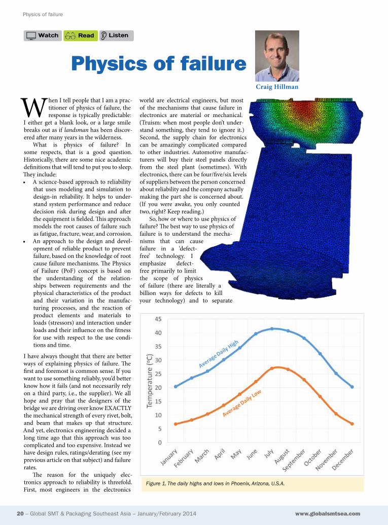
Once you know the mechanisms, then comes the hard part. You need to figure out the environment the product will experi-ence over time. Temperature, humidity, shock, vibration, voltage, power, current, etc. All this stuff needs to be figured out in some detail. A great example is the graph in Figure 1 showing the daily highs and lows in Phoenix, Arizona, in the United States.
Now, you might be asking, why is Phoenix, Arizona a great example? For one, Phoenix is hot. Really hot. And Phoenix is also really cool (side benefit of being in the desert). These high temperatures and large temperature swings (note that almost every day sees a 15˚C change in temperature) can do a good job of accelerating different failure mechanisms. But, most importantly, Phoenix is a big city with lots of people who buy lots of electronics. Which means, that for most electronics used outdoors, Phoenix is a good representation of real-istic worst-case conditions. You could try to do a prediction for a 15-year lifetime in the Gobi desert, but what’s the point?
Once you know your mechanisms and your environment, you are ready to go. Except, most companies have a slight problem. As seen in the previous discus-sion, there can be three, five, seven or even more failure mechanisms per part, and
there can be hundreds if not thousands of parts on a board. With most equations requiring a half-dozen different param-eters, a physics of failure practitioner could be looking at gathering over 50,000 pieces of data to perform 10,000 different calcula-tions.
And this, more than anything else, is what has driven physics of failure into a closeted activity. It’s not that the industry does not see value in the practice. It’s just that the requirements to perform such an activity has led the industry to find effec-tive substitutions and to limit physics of failure to technologies of concern or during radical changes in design or mate-rials.
The eventual goal of every high reli-ability organization should be life curves for every relevant technology (remember, not every technology degrades over time). This, far beyond our current approach, would create electronics as safe and effec-tive as that bridge we drive over everyday.
Craig Hillman is CEO and Managing Member for DfR Solutions. Dr. Hillman’s specialties include best practices in Design for Reliability (DfR), Pb-Free strategies for transitioning to Pb-free, supplier qualifica-tion (commodity and engineered products), passive component technology (capacitors, resistors, etc.), and printed board failure mechanisms. Dr. Hillman has over 40 Publications and has presented on a wide variety of reliability issues to over 250 companies and organizations.

22 – Global SMT & Packaging Southeast Asia – January/February 2014 www.globalsmtsea.com
2013 ends on a high note
Although business conditions were weak for much of last year they “ended with a bang.”
Electronic equipment shipments were up 6% globally in December 2013 vs. December 2012 (Chart 1) driven by a strong year end surge in SE Asia. The normal winter seasonal slowing was not yet evident in December based upon equip-ment shipments.
Components (which “lead” electronic equipment by about month in the business cycle), did peak in November. Printed cir-cuit board sales edged down in December (Chart 2) and will likely continue to decline throughout the first quarter of this year.
Semiconductor shipments also finished last year on a positive note (Chart 3). They were up 6.8% on a 3-month average basis in November versus the same period in 2012 with shipments to N. America up a whop-ping 18.6%.
The N. American electronic supply chain finished 2013 on generally good terms. Chart 4 shows the annualized (12/12) and 3-month (3/12) growth rates for November vs. the same period a year earlier. A value of 100 indicates no change. Except for passive component orders and shipments and computer orders all other categories were growing. Domestic elec-tronic equipment orders rose 5.7% on a 3/12 basis in November 2013.
Thanks to our colleague Ed Henderson Charts 5 & 6 provide his latest forecasts for GDP and electronic equipment growth by region by year. At this point 2014 looks like a year of solid “single digit” growth. World• IT spending is on pace to grow 3.1% y/y
to $3.8 trillion in 2014.—Gartner• Technology sales reached $282 bil-
lion in China in 2013, surpassing North American, which purchased
$257 billion.—Consumer Electronics Association
• Technology spending will rise 6.2% y/y to US$2.22 trillion in 2014.—Forrester
• Regional• China smartphone sales will top 436
million units in 2014, with local hand-set suppliers shipping 279 million units.—Digitimes Research
• China-based makers are expected ship 575 million touch panels for smart-phones, 165 million units for tablets and 10 million units for notebooks in 2014.—Digitimes Research
Mobile communications worldwide com-bined shipments of devices (PCs, tablets, ultramobiles and mobile phones) are pro-jected to grow 7.6% y/y to 2.5 billion units in 2014.—GartnerComputers & peripherals• PC shipments declined 6.9% y/y to 82.6
million units in 4Q13.—Gartner• Tablets shipments will increase from
141 million in 2012 to 243 million units in 2014 and 488 million in 2017. – HIS
• LCD monitor shipments will drop 5.1% y/y to 150 million units in 2014.—WitsView
Consumer electronics manufacturing rev-enue is forecast to fall 2% y/y to $250.0 bil-lion in 2014. – HISAutomotive • sales will rise 4% y/y to 87.4 million
light vehicles in 2014.—Deutsche Bank• TFT LCD shipments are expected to
grow from 65 million units in 2013 to more than 90 million units in 2017.—NPD DisplaySearch
• self-driving cars will grow from nearly 230 thousand in 2025 to 11.8 million in 2035.—IHS
Medical electronics • sales will grow 8% y/y to about $50.9
billion in 2014 after rising 3% y/y in 2013 to $47.3 billion.—IC Insights
• home healthcare applications sensor market to grow from $559M in 2013 to $1.2B by 2018.—Yole Développement
Military electronics • land vehicle electronics market is fore-
cast to hit $3.3B in 2014.—Visiongain
Walt Custer and Jon Custer-Topai
2013 ends on a high note
World Electronic Equipment Monthly Shipments
Converted @ Constant 2012 Exchange Rates
Source: Custer Consulting Group & Electronic Outlook Corp
20140114
0102030405060708090
100
Jan
May
Sep
Jan
May
Sep
Jan
May
Sep
Jan
May
Sep
Jan
May
Sep
Jan
May
Sep
Jan
May
Sep
Jan
May
Sep
Jan
May
Sep
Jan
May
Sep
Jan
May
Sep
Jan
May
Sep
Jan
2002 2003 2004 2005 2006 2007 2008 2009 2010 2011 2012 2013 2014
USA
W Europe
Japan
Taiwan+China
ROA
ROW
US$ B
Chart 1.
Read ListenWatch

Global SMT & Packaging Southeast Asia – January/February 2014 – 23www.globalsmtsea.com
2013 ends on a high note
• & Aerospace industry will grow 5% y/y to U.S. $1.4 billion in 2014.—Deloitte Touche Tohmatsu
Digital cameras • module market will grow at a 19.7%
CAGR between 2013 and 2019 from US $12 billion in 2012 to US $43.06 billion in 2019.—Transparency Market Research
• compact sales are likely to fall more than 40% y/y to fewer than 59 million units in 2014.—IDC
Flat panel displays• LCD TV shipments will grow 3% y/y
to 209.1 million units in 2014 after fall-ing 1.7% y/y to 203.1 million units in 2013.—WitsView
• 4K×2K TV shipments are expected to grow from 1.9 million units in 2013 to 12.7 million units in 2014.—NPD DisplaySearch
• TFT LCD area demand will increase 9%, from 141 million m² in 2013 to 154 million m² in 2014.—NPD DisplaySearch
• AMOLED light-emitting materials will expand from US$350 million in 2013
to US$445 million in 2014.—IHS LED lighting• sales are expected to increase 15-20%
as prices drop 20% through 2015. – HIS• applications will increase from $3.6 bil-
lion in 2013 to $5.6 billion in 2014 and $7 billion by 2016. – HIS
RFID market will grow from $7.88 billion in 2013 to $9.2 billion in 2014.—Bharat Book BureauSmart technology• Internet of Things installed base will
grow to 26 billion units by 2020, with incremental revenue exceeding $300 billion.—Gartner
• gesture-sensing smart devices will expand nearly 70% y/y to nearly 330 million in 2015.—NPD DisplaySearch
• motion control product sales hit $12.2 billion in 2013.—IHS
• intelligent lighting sensors and net-work control gear will grow from $1.1 billion in 2013 to nearly $2.7 billion by 2020.—Navigant Research
Wearable devices • for infotainment application shipments
will rise by 155% from 51.2 million in
2013 to 130.7 million units in 2018.—HIS
• for fitness market reached over $330 million in 2013.—NPD Group
• Video gaming market is forecast to grow 11.1% y/y from 53.9 billion Euros (US$73.8 billion) in 2013 to 82.1 bil-lion Euros in 2017.—IDATE
Electronic waste weight will rise from 48.9 million tons in 2012 to 65.4 million tons in 2017, with most of the growth in develop-ing nations.—StEP
ems, oDm & related assembly activityNorth America EMS growth is expected to decline 0.4% to $45.5 billion in 2014.—IHSTop five contract makers’ (Quanta, Compal Electronics, Wistron, Inventec and Pegatron) notebook shipments grew 4% q/q to 37.23 million units in 4Q13.—Morgan StanleyCicor Electronic Solutions and Cicor Asia divisions were merged into “Electronic Solutions” division.
World PCB Monthly ShipmentsConverted @ Fluctuating Exchange Rates
20140110
0.0
0.5
1.0
1.5
2.0
2.5
3.0
3.5
Jan
May
Sep
Jan
May
Sep
Jan
May
Sep
Jan
May
Sep
Jan
May
Sep
Jan
May
Sep
Jan
May
Sep
Jan
May
Sep
Jan
May
Sep
Jan
May
Sep
Jan
May
Sep
Jan
May
Sep
Jan
May
Sep
Jan
May
Sep
Jan
00 01 02 03 04 05 06 07 08 09 10 11 12 13 14
N AmericaEuropeJapanTaiwan/ChinaRest of AsiaKorea
$ Billions
Source: Custer Consulting GroupCalendar Year
Chart 2.
11/12 11/13 % CH
Americas 5.02 5.95 +18.6%
Europe 2.80 3.11 +10.9%
Japan 3.41 3.11 - 8.8%
Asia Pacific 14.28 15.07 + 5.6%
Total 25.51 27.24 + 6.8%
Monthly Semiconductor Shipments$ Billions (3-month average)
SIA www.sia-online.org/
20140102
Chart 3.
Latest Annual 3-Month Month Growth Growth
Electronic Component $Rigid & Flex PCB Orders (N Amer) 11/13 98.9 101.3Rigid & Flex PCB Shipments (N Amer) 11/13 96.6 102.1Electronic Component Orders 11/13 97.8 97.8Electronic Component Shipments 11/13 97.3 99.4Semiconductor Shipments to N America 11/13 111.9 118.6
U.S. Electronic Equipment Orders $Computer & Related 11/13 92.7 91.8Communication 11/13 107.7 108.4Medical, Measurement & Control 11/13 96.3 108.6Search & Navigation 11/13 92.6 107.3Defense Capital Goods 11/13 101.4 103.0Military Electronics 11/13 90.6 108.4Total Electronic Equipment 11/13 97.4 105.7
U.S. Industrial Production 11/13 102.5 103.3
NOTE: 3 month growth rates compare most recent 3 months to same 3 months one year earlier
Present Growth Rates (%)20140114
U.S. Economy & Electronics Industry
Chart 4.
World 2.5 2.4 3.2 3.9 3.7
USA 2.8 1.8 2.7 3.4 3.3
EU -0.4 -0.1 1.1 1.5 2.0
Japan 1.4 1.9 2.0 1.6 1.2
Four Tigers 1.9 2.5 3.6 4.0 3.8
China 7.7 7.6 7.9 8.4 7.7
Henderson Ventures 1/2014www.hendersonventures.com
2012 2013 2014 2015 2016
GDP GrowthConstant $ Growth Rates Converted @ Constant Exchange Rates
20140114
Chart 5.

24 – Global SMT & Packaging Southeast Asia – January/February 2014 www.globalsmtsea.com
2013 ends on a high note
Computrol is celebrating its 30-year anni-versary in 2014.Connect Group obtained ISO 13485 med-ical certificate for its facility in Poperinge Belgium.DfR Solutions entered government/mili-tary equipment collaboration with Circuit Solutions.ESCATEC Switzerland became a found-ing member of the professional group “Photonics” at SWISSMEM.Express Manufacturing Inc. • subsidiary, EMI Asia Limited received
EN/JISQ/ AS9100:2009.• added smaller packaging manufactur-
ing technologies and NPI program will shorten time-to-market for medical devices.
Foxconn/Hon Hai • is building a panel and touchscreen
technology R&D center in Hsinchu, Taiwan.
• launched investment fund will finance startups developing new kinds of wear-able computers.
• started operations at first store-factory complex in Quiyang, China.
• began production at its new demon-stration plant in Guiyang, China.
• plans to build a handset plant in Indonesia’s Jakarta or the Yogyakarta Special region.
• is moving 60-inch and 70-inch flat-screen TV manufacturing from Mexico to U.S.
Global-Tech Advanced Innovations ended EMS Business operations.Jabil sold its aftermarket services business to iQor for $725 million.
JJS manufacturing launched new website, www.jjsmanufacturing.com.Kimball International appointed Lonnie Nicholson, CIO and Timothy Jahnke to the Company’s Board of Directors.Kitron terminated plan to establish common distribution center.
Lite-On Technology merged with Leotek Electronics, Lite-On Clean Energy Technology, MET opened a manufacturing facility in Melbourne, Florida.Michigan Manufacturing International opened new HQ in Stevensville, Maryland.Microtek Labs opened new test facility in Linthicum Heights, Maryland.NATEL named Warren Dannelly, Director of Sales and Victor Yamauchi, VP of Continuous Improvement.Neways Electronics Production closed and transferred all Kassel, Germany pro-duction activities to other Neways operat-
ing companies.Nortech Systems appointed Richard Wasielewski, President and CEO.Pegatron chairman, TH Tung was named Taipei Computer Association Chairman.Permatech added a Siemens SIPLACE POE S27 pick and place machine.Sanmina appointed Michael Clarke and Eugene Delaney to Board of Directors.SMTC appointed Sushil Dhiman, President and CEO.STI Electronics opened new IPC approved training center in Houston, Texas.Surface Mount Technologies, Inc. teamed with Eruston to offer complete turnkey manufacturing.Surface Technology International received £11.5million financing package from Lloyds Bank Commercial BankingSymprotek added high performance production line from APEX Factory Automation which includes: SJ Inno Tech 3D printer, SJ Inno Tech HP-520SPI, cTS-Monvection reflow and Mirae Mx400L and Mx400LP placement machines.TT electronics • relocated Werne, Germany manufac-
turing operations to lower cost regions.• IMS opened 50,000 SF manufacturing
facility in Timisoara, Romania.VirTex Enterprises acquired MTI Electronics.
PCB fabricationGlobal brand motherboard shipments fell from 80 million units in 2012 to 75 million units in 2013; Asustek Computer and Gigabyte Technology will aggres-sively compete for the number-one spot in 2014.—DigitimesTop 5 PCB makers in 2013 that achieved sales revenues greater than $2 billion are: Nippon Mektron, Unimicron, Samsung Electro-Mechanics, Young Poong Group and Zhen Ding Technology.—Dr. Hayao NakaharaADCO Circuits purchased a second Ersa selective soldering machine.AT&S • appointed Karl Asamer, CFO.• closed its Klagenfurt, Austria facility.Circuit Technology Inc. opened a training center in Melbourne, Florida.Compeq first-phase construction of new Chongqing, China plant is expected to be completed in mid-2014 with an installed capacity of 200,000-300,000 SF of HDI boards.Diagnosys appointed Sergio Moreno VP Sales, Latin America.Eagle Circuits received Integral Technology’s Zeta® certification.Greule filed for insolvency.
World 1.0 -2.6 4.8 6.0 5.8
USA -0.9 -3.4 3.0 5.0 5.2
W. Europe -3.4 -5.2 1.5 3.4 3.8
Japan -2.6 -8.6 3.5 4.4 3.6
Four Tigers -1.2 1.8 4.6 5.8 5.2
China 2.6 -2.3 6.4 7.1 6.5
Henderson Ventures 1/2014www.hendersonventures.com
2012 2013 2014 2015 2016
Electronic Equipment Production Growth
Constant $ Growth Rates Converted @ Constant Exchange Rates
20140114
Chart 6.
The North American electronic supply chain finished 2013 on generally good terms.

Global SMT & Packaging Southeast Asia – January/February 2014 – 25www.globalsmtsea.com
2013 ends on a high note
GUH Holdings spent RM20mil to expand its Penang and Suzhou plants by about 50% to 807,000 SF.Ibiden is investing $400 million into a second HDI plant in Malaysia.Icape Group became fully compliant to “conflict-free minerals” regulations.Mitsubishi Material developed DBA printed circuit board with thick copper conductors for the next generation power modules.Nanya PCB invested NT$1.5 billion to expand FC CSP substrate capacity in 2013.NCAB Group Germany appointed Heinie von Michaelis, Managing DirectorPanasonic will discontinue production of ALIVH boards in 2014.Q.P.I. Circuits and Q.P.I. Electronic Design Automatisation merged into new subsidiary, Q.P.I. Group B.V.RASP moved from South Glens Falls to 22,000 SF building in Moreau, New York.Schweizer Electronic • and Elekonta entered collaboration for
HDI, thick copper, HF and impedance-controlled PCBs.
• received EN 9100 aerospace industry certification.
SEMCO is building a new HDI plant in Vietnam.Spirit Circuits acquired Lyncolec.Taiwan PCB Techvest expanded monthly production capacity in Chongqing, China to 900,000 SF in 2013.Tramonto Circuits named John Talbot, President.Twisted Traces moved to new facility in Elk Grove Village, Illinois.Unimicron is investing $500 million to build an IC substrate manufacturing plant in Kweishan, Taiwan.Unitech plans to increase its HDI board production capacity by removing bottle-necks in 2014.
materials, process & test equipmentSMT equipment market to reach a global value of $5.3 billion by 2018; Latin America will grow at a 7.2% CAGR of over the next five years.—Global Industry AnalystsAgilent Technologies named the elec-tronic measurement company it expects to spin off in early November 2014, Keysight Technologies.Air Products and Chemicals opened a manufacturing facility in Manatee County, Florida.Alpha’s Altoona, Pennsylvania, facility was certified as compliant conflict-free smelter.Atotech won patent infringement lawsuit
in Taiwan for Stannatech® process and equipment.Camtek Board reappointed Rafi Amit, CEO.Cogiscan is celebrating 15-year anniver-sary.CyberOptics appointed Executive Chairman Subodh Kulkarni as interim CEO after Kathleen Iverson retired.Datest is commemorating 30 years in busi-ness in 2014.Dymax hired Paul Rachielles as Global Marketing Manager.ETI/NEA expanded its production floor by 40% at its Hudson, New Hampshire facility.Eucon Holding ended laser drilling opera-tions.
GOEPEL electronic and Teradyne devel-oped an extended Boundary Scan option for production In-Circuit Test/Functional Board Test of PCBs and the modular func-tional testers on VXI and PXI Express basis.Isola • transitioned manufacturing of its low-
loss, I-Speed material to Asia.• Suzhou plant received ISO/TS 16949
certification.JUKI unveiled optical inspection machine “RV-1” for component mounted circuit boards.Korean SMT Solutions began electronics equipment assembly distribution opera-tions for Estonia, Lithuania and Latvia, Russia, Ukraine, Belorussia, Moldova, Kazakhstan.LPKF acquired outstanding shares in Slovenian subsidiary LPKF Laser & Elektronika Naklo, Slovenia.Marubeni co-developed a new fine line printing process using sub-micron gold powder which is bondable at 200 degree C and heat resistant at 300 degree C.Niching Industrial spent NT$125 million (US$4.16 million) to purchase building to set up nano silver paste production lines.Nordson Advanced Technology Systems moved to new facility in New Taipei City,
Taiwan.OK International appointed Christopher Larocca, President.Orbotech Korea employees were acquit-ted on charges of theft of corporate secrets from LG and Samsung.Toppan Forms developed new silver print-ing process with very low firing tempera-ture (80˚C) using silver salt ink.
semiconductors & other ComponentsGlobal semiconductor sales increased 4.9% to $317.9 billion in 2013.—IHS pre-liminary estimateDRAM chip production is expected to increase 32.5% y/y to US$35.2 billion in 2013, after contracting 24.6% in 2011 and 9.8% in 2012.—TrendForceFlip chip technology market is reached $20.1 billion in 2013.—BCC ResearchHigh-brightness LED chip production will increase 129% y/y to US$12.743 billion in 2014. -DigitimesMagnetic sensors market revenues are forecast to grow from $1.66 billion in 2012 to $3.51 billion in 2019 on smartphone and automotive segments.—Frost & SullivanMicrocontroller market revenue will grow 15% y/y to US$17 billion in 2014 driven by internet of things, solar, smart-home, and electric vehicles.—EMITT SolutionsNAND Flash revenue will grow by 13% y/y to $28 billion in 2014.—DRAMeXchangePower semiconductor discretes and mod-ules revenue reached slightly less than $15 billion in 2013.—IHSPower semiconductors in the automo-tive industry will grow from $2.81 billion in 2012 to $5.28 billion in 2018.—Frost & Sullivan
Walt Custer is an independent consultant who monitors and offers a daily news service and market reports on the PCB and assembly automation and semiconductor industries. He can be contacted at [email protected] or visit www.custerconsulting.com.
Jon Custer-Topai is vice president of Custer Consulting Group and responsible for the corporation’s market research and news analysis activities. Jon can be contacted at [email protected].
At this point 2014 looks like a year of solid “single digit” growth.

Title
26 – Global SMT & Packaging Southeast Asia – January/February 2014 www.globalsmtsea.com
Kirsten has just introduced a fascinating new modular wave system, the modula wave®. What can you tell us about it, Zoltàn?
This system was actually put on the mar-keting six years ago, but now we’ve come out with a new revision based on feedback from our customers. The changes we made were designed to make the user’s life easier.
First of all, we changed our conveyor system. Now we are using an adjustable-width pin chain conveyor that can accom-modate any size of industry-wide used frames, including those from most of our competitors, without any kind of changes. The frames can be identified with a label. When you put a new frame on the input conveyor, the software loads the appro-priate program based on this identification label.
So you have a bar code reader mounted there.
That’s correct. It’s a standard feature for the machine. Based on the label, the software loads the production program and selects all the parameters for the product.
We also provide our customers with a feature to change to PCB manufacturing, on a raw PCB without a frame. In this case, you need to change to the finger conveyor, the conveyor system above the soldering module.
interview
Interview—Zoltàn Sopsits, Kirsten solderingAt Productronica, Trevor Galbraith got a thorough introduction to the latest upgrades made to Kirsten Soldering’s modula wave® system. Zoltàn Sopsits, East European Sales Manager for Kirsten Soldering AG, gave him the tour.

Global SMT & Packaging Southeast Asia – January/February 2014 – 27www.globalsmtsea.com
Title
With this system, every module has its independent conveyor system. That means the speed can be set indepen-dently for each module.
Right. You have five different stages on this demonstration model.
This is our minimum configuration. It includes an input conveyor, a flux module, a preheater, a solder module, and an output conveyor. So the program is loaded and the frame arrives at the fluxer. The fluxer speed and pressure and the conveyor speed are all calculated automatically by the software. The process engineer just has to enter into the software how much flux they want in the area. The rest is the software’s job.
On this demonstration system, we have a two-head spray fluxer. It repre-sents two independent pump and pressure control systems. So, without a changeover, two different types of flux can be used with a single fluxer module. The two tanks and pumps, each with its own pressure control, are accessed from this drawer at the front of the module.
These tanks can have the same flux or dif-ferent fluxes.
Yes, at the same time in the system, so that products and batches can be mixed. As I said, when the frames are identified the software decides which recipe to load into the software.
Moving on to the heating stage. Looking at it, you may say, What would these guys want with a 60-centimeter preheating that is good for nothing? And you’re absolutely right if you consider that the competitor’s machine has only one chain system. The conveyor speed in that situation must be fixed on the soldering speed. With those systems, you have to keep moving. Here not. You can stop. We can simulate in one module the complete preheating phase to reach the proper preheating temperature and activate the flux.
It’s an interesting way that you’re actu-ally applying the heat here. You’re using a new, patented system for it.
Our new system is quite close to reflow technology. We’ve got a mesh plate. We are pushing through the mesh plate high pres-sure air and creating a kind of convective heating. But how we are heating is different. We are heating only these smooth tiny steel plates above and below the conveyor with hundred of amps, heating it up to 450˚ to 500˚ C.
So it’s essentially just a steel plate.
It’s just a steel plate, there is no heater behind it. We are heating the plate itself. And since this has a very, very small ther-mal mass, the heating up and adjusting time is just minutes—seconds actually.
It’s a very fast ramp-up and accurate con-trol.
Exactly. That’s the aim of this construction. And this is really a brand-new construc-tion. We just patented it this year.
Finally we move on to the wave itself and the bath.
After the preheat zone, which can be one, two or even three modules, we reach the soldering station. Here it is a single module, but we can deliver the machine with two. So if the production requires dedicated use of a special tin for a customer with small batches, you don’t need to have a complete full-blown line. It’s enough to buy 65-centimeters of module. You can turn it on whenever you want, and you can change the tin whenever you want because the pot contains only 65-kilograms of tin.
Now the pot construction is interesting. The method of heating—it doesn’t have any impellers in the bath. As you said, it’s a fairly small size. How are you actually heating and controlling the solder in the bath?
Below this cast iron pot, there is a linear motor. The linear motor doing wave is not a new technology for us. Kirsten from the beginning has used this technology, so we have 30 years experience with this. The linear motor has the benefit that it’s moving without any moving parts, so we are pumping the tin in the bottom of the pot in channels up to the nozzle base. And here comes our new development: now we introduce to the market an interchange-able nozzle top that allows the customer to use different angles and different flow speeds for the soldering.
So you can use different-shaped waves, basically?
The shape of the wave is still the same. It’s a hollow wave, but by changing the nozzle dimension we can have a different flow speed and different wave height.
Can you also control the Z-height of the wave electronically?
Yes. Most of our competitors’ machines have two defined heights, one for opera-tion and one for maintenance. We have a free parameter on the pot height, allowing
the process engineer to set whatever is the best for the soldering.
This machine is equipped with nitrogen cover. We also have a unique feature to have a anti-dross liquid cover above the pot. That is a little more cost-effective than the nitrogen; in our Eastern market, they prefer it to the nitrogen cover. It’s a synthetic oil-based material that is quite good for protecting the molten solder surface.
At the end of the machine, we’ve got an output conveyor. Nothing special about that, but here is the point that I have to mention one more feature, and that’s the pendulum mod. When the frame has finished processing, it’s returned to the front. With this, you could put the machine in the corner of the factory. You don’t have to come to the other end. If you want to build a small batch, you can have one touch-up operator at the front who may even assemble the board.
How does it do that?
That’s a software feature. The frame arrives at the end, and as the entry sensor is acti-vated, the frame goes back to the front. This is especially useful for the small batch production. This demonstration machine is not a full-blown system. We offer the system with return conveyor and with lift-ers, working stations, everything.
That’s an interesting look into this new system, Zoltàn. I want to thank you very much for spending the time with us today.
—Trevor Galbraith
interview

Title
28 – Global SMT & Packaging Southeast Asia – January/February 2014 www.globalsmtsea.com
Brief review of 20132013 saw a major mile-stone achieved in the Indian Electronics Industry with the “SMTA India Chapter” formation in August. The Chapter, located in Bangalore, started off with activities in September, with the “Kick-Off Meeting” at Chancerry Pavillion.
SMTA India Chapter had been consistently honoured to have Industry stalwarts as the Guests of Honour. We had Mr.Arnob Roy, VP Engineer, Tejas Networks enthralling the audience during the Kick-off Meeting in September with his enthralling speech on “The Opportunity for Electronics System Design and Manufacturing”.
In the December Quarterly Meet Dr. Anand Narasimhan, of “SIMS Recycling Solutions”, highlighted the importance of the end-recovery mechanism of the
Electronics Value Chain.SMTA India Chapter also highly
values its association with IPC India and was grateful to have the gracious presence of Mr.A Vijayendra, during the SMTA Kick-Off Meet.
The Chapter also values its associa-tion with various media houses and shares
special relation with Global SMT & Packaging magazine.
look forward in 2014SMTA India Chapter contin-ues its efforts in 2014 through its events and is all set to intro-duce the SMTA Certification Program: “Certified SMT Process Engineer” in India during Q2 2014.
The Chapter details are continuously updated on the Chapter’s webpage. See http://smta.org/chapters/chapters_detail.cfm?chapter_id=123
For further details get in touch with Rajeev Kulkarni
(Chapter President): [email protected], or Ankan Mitra (Chapter Vice-President): [email protected].
SMta india Chapter round-UpSMTA india chapter round-up
A Year in Review: 2013
Topic Speaker EventThe opportunity for electronics System Design and Manufacturing
Arnob royVP engineering, Tejas networks
Kick-off Meet
Pcb vs PcbA Process challenges & Solutions
richard Puthota Alent - india
Kick-off Meet
System reliability and challenges of electronics industry
Pankaj bansod Diebold, india
Kick-off Meet
Alternate Alloys liyakathali Koorithodi indium corporation
Kick-off Meet
Frontiers in electronics Manufacturing Ankan Mitra SMTA india chapter
Kick-off Meet
challenges with MSD components and its Future
Ankan Mitra SMTA india chapter
october luncheon Meeting
DFM and DFA Ankan Mitra SMTA india chapter
november luncheon Meeting
e-waste challenges and Solutions Dr. Anand narasimhanSiMS recycling Solutions
December Quarterly event
PiT Manufacturing Process and control T Durga SagarPro-innovative Technologies
December Quarterly event
Pcb Protection M P rajaramhenkel, india
December Quarterly event
Solutions big Data Analytics & electron-ics System Design
Ankan Mitra SMTA india chapter
December Quarterly event
summary of smta india chapter topics & speakers in 2013

Global SMT & Packaging Southeast Asia – January/February 2014 – 29www.globalsmtsea.com
india attracts over uSD 10 billion investment proposals under M-SiPS in 2013
Over the last couple of decades India has been the epicentre of consumer demand fuelled by a
phenomenal 8% plus GDP growth. While demand increased across all sectors, demand for high technology products, spe-cifically electronic products has registered significant growth and going by current estimates, the demand for electronics hard-ware in the country is projected to increase to USD 400 billion by 2020, according to the Ministry’s 2010 Task Force Report.
The estimated electronics production will reach USD 104 billion by the year 2020, creating a gap of USD 296 billion in demand and production. This creates a unique opportunity for companies in the ESDM (Electronic System Design & Manufacturing) sector to look at India as their next destination to cater to the domestic Indian demand as well as act as an exports hub.
Accordingly, the Government had notified the Modified Special Incentive Package Scheme (M-SIPS) in July 2012 to attractive investments in high-tech elec-tronics manufacturing in India. The incen-tives under the M-SIPS investment will be available for investment made for new units/ expansion/ relocation/diversifica-tion and modernization of existing elec-tronics manufacturing units. The incentive would be available within 10 years of the approval of the new electronics system design & manufacturing (ESDM) unit, and not with regard to any subsequent phase/s of the project.
Under the M-SIPS, the companies investing in India would be allowed duty free import capital equipment for setting up units in Special Economic Zones (SEZ), and would get reimbursement of CVD/excise duty for capital equipment in non-SEZs. Also, the companies would get 25% subsidy on Capex in non-SEZs units and 20% subsidy on Capex for setting up manufacturing unit in SEZs over a period
of 10 years. As on 26 January 2014, the Department
of Electronics & IT (DeitY) has received investment proposals worth over INR 65,000 crores (USD 10 Bn) in the following sectors:• Semiconductor FAB: INR 52,000 Cr.• Telecom Products/Handsets: INR 8,218
Cr• LED FAB/LED Lighting: INR 1,991 Cr• Consumer Electronics/Appliances:
INR 791 Cr• Automotive Electronics: INR 706 Cr• Other verticals: INR 1,081 CrThe M-SIPS would be open for applications for 3 years from the date of the notifica-tion—27 July 2012. The incentive will be available for units set up within Electronics Manufacturing Clusters notified by the DeitY.
The list of 30 notified Brownfield Electronics Manufacturing Clusters in India for M–SIPS Scheme is available at http://deity.gov.in/content/electronic-hard-ware.
I am happy to see, some of these policy announcements are bearing fruit, particularly the Modified Special Incentive Package Scheme (M-SIPS 2012) to attrac-tive investments in the high-tech electronic manufacturing in India. As on 26 January 2014, the DeitY has received investment proposals worth over INR 65,000 crores (USD 10.5 Billion) in the sectors like semiconductor FABs (INR 52,000 Cr.), telecom products/handsets (INR 8,218 Cr.), LED FAB/LED Lighting (INR 1,991 Cr.), consumer electronics/appliances (INR 791 Cr.), automotive electronics (INR 706 Cr.) and other verticals accounts for INR 1,081 Cr. These figures represent a statis-tical achievement for the government on the occasion of 65th Republic Day of India. I am sure the approval for some of these investment proposals is already given, and the rest are under evaluation. But the most crucial aspect is, DeitY is yet to
complete the process of selecting a finan-cial institution for third party appraisal of select investment proposals received under M-SIPS. So, once government closes this missing link, we will see the actual inflow of investments in the Indian ESDM sector. I am sure these investments will create a ripple effect across the manufacturing value chain and help in building an atmo-sphere for high-tech electronics manufac-turing in the country.
The Government’s Preferential Market Access (PMA) policy for providing prefer-ence to certain domestically manufactured electronic goods is another noteworthy initiative. I also applaud DeitY’s announce-ment of specific schemes such as IT Investment Region (ITIR) near Bangalore; notification of 30 Brownfield Electronic Manufacturing Clusters (EMC) and
“In-principal” approval of 7 new Greenfield Electronic Manufacturing Clusters are right steps to speed-up the sector in India, which is otherwise delayed due to land acquisition issues and green clearances. We should also hasten the process for high-tech innovators like Japan, Taiwan, Korea and China to set up “Country specific EMC”s under the Bi-lateral Trade Agreements in the country. There should be a “Single Window” clearance for setting up these “Overseas Manufacturing Enclaves” in any of the government approved EMC’s across the country.
india attracts over usD 10 billion investment proposals under m-siPs in 2013Debasish Choudhury
Read ListenWatch

Title
30 – Global SMT & Packaging Southeast Asia – January/February 2014 www.globalsmtsea.com
new in-Sight software release features advanced defect detection tools
Cognex Corporation releases In-Sight® Explorer 4.9, software that offers an expanded set of inspection tools and an enhanced Cognex Connect™ communica-tions suite featuring the iQ Sensor Solution network (iQSS). This latest version of In-Sight Explorer software includes the surface flaw tool and the scene correction
filter. The Cognex Connect suite of fac-tory communication protocols ensures that In-Sight vision systems can easily commu-nicate with a broad range of devices on the factory floor. www.cognex.com
HDi microvia PcBs now available online at WedirektThe HDI specialist Würth Elektronik has added HDI microvia PCBs to the com-pany’s online shop, WEdirekt. With just a few clicks, your HDI PCB is calculated and the price is shown immediately online. Ordering prototypes is considerably sim-plified and faster. Normally, the following statement applies: low quantity required plus a complicated production process results in high costs. This is not so at Würth
Elektronik. Due to its mass of experi-ence, the PCB manufacturer is a specialist in the field HDI and has now expanded its online shop with this technology. www.we-online.com
Laird expands eMi shielding portfolio with edge guide clip-on Strip
Laird releases a new Fingerstock product, the Edge Guide Clip-on Strip. Ideal for virtually every application where Printed Circuit Boards (PCBs) need to be grounded and/or shielded, this new product reduces installation and labor costs and is available in custom lengths. A customer installing a 10 cm, or 8 finger strip, could reduce instal-lation time by up to 80% using the Edge Guide Clip-on Strip as opposed to per-forming a typical installation with 8 tradi-tional single clips. www.lairdtech.com
Handheld dispensing valve features low maintenance, internal diaphragm design The new Dymax Model 300 dispensing system features a pneumatic, normally closed diaphragm valve that is designed for use with low- to medium-viscosity fluids. The valve’s diaphragm design prevents fluid from contacting the actuating com-ponents within the valve, reducing com-ponent damage and wear while extending
new productsnew products
Vj electronix introduces the new X-Quik benchtop X-rayVJ Electronix, Inc., debuts a new low-cost, easy-to-use X-ray inspection system—the X-Quik. The X-Quik is a small, general-purpose X-ray system for inspection of items such as electro-mechanical devices, sensors, molded parts, mail parcels and biological samples. With a size of just more than two feet cubed and a low, affordable price point, the X-Quik is well suited for engineering labs, machine shops and quality control departments for a wide variety of applications. www.vjelectronix.com

Global SMT & Packaging Southeast Asia – January/February 2014 – 31www.globalsmtsea.com
Title
the life of the valve. It also features a mate-rial flow adjustment to accurately control shot volume, and its lightweight, compact design makes it comfortable and easy to handle. www.dymax.com
Power modules get their own upside-down C-SaM® system Sonoscan has shipped the first of its new D9600Z C-SAM® systems. This new model is designed expressly to facilitate the imaging of IGBT (Insulated Gate Bipolar Transistor) power modules. Power mod-ules, such as IGBTs, are basically high-speed high-power switches used in railway engines, electric automobiles, and many other applications involving high power. Prior to packaging the transistors them-selves are at the top of the module and are too susceptible to water contact to permit acoustic imaging from above.www.sonoscan.com
innovative sensors require advanced test equipment
Multitest announces that its leading solu-tion for 3-axis magnetometer plus 2-axis low g-test and calibration fully supports the technical features of today’s advanced 3D hall sensors. The modular concept for sensor test equipment ensures the most economic equipment utilization. The system has been designed for the industrial and automotive market segments. Both
require the highest accuracy and preci-sion as well as the full temperature scope of ambient-hot-cold. www.multitest.com toughened two component epoxy is optically clear and resists thermal cyclingMaster Bond EP38CL was developed for bonding, sealing, coating and encapsula-tion applications that require toughness and durability. With a Shore D hardness exceeding 75, its toughness is a unique property that imparts resistance to rigor-ous thermal cycling, impact and mechani-cal shock. www.masterbond.com
goePeL electronic improves flexibility of raPido™ inline systems for programming and test
GOEPEL electronic announces the avail-ability of new features in the RAPIDO™ multi-site inline production system family for high-speed in-system program-ming and board test based on the latest Embedded System Access (ESA) technolo-gies. One of the essential innovations is an option to utilize planar downholders in sandwich construction. Now ultra-thin, rigid-flexible boards with contact gaps of up to 50 mil can be safely handled in mul-tiple-up production. Utilizing this tech-nology, RAPIDO has become one of only a few systems that meet the challenges of safe inline contacting for such sensitive applications. www.goepel.com
advanced dual-cure conformal coating from intertronicsIntertronics announces the DYMAX Dual-Cure 9482, a UV light- and moisture-cure conformal coating specially formulated to flow underneath components on printed circuit boards and cure in these shadowed areas by using ambient moisture, which can result in faster throughput for through hole assemblies. DYMAX 9482 coating demon-strates excellent re-workability which is of particular importance to manufacturers of expensive PCBs or manufacturers looking to increase board yields. Typical applica-tions include electronic assemblies for the general and consumer electronics, auto-motive, appliance, and military equipment manufacturing industries.www.intertronics.co.uk
mt2168—successful evaluation proves superior performance
Multitest announces that it received the official data from an evaluation of the MT2168 that confirms the superior perfor-mance of the MT2168 pick-and-place han-dler. During this evaluation on an HVM test floor in Asia, more than 2.3 million packages were handled. The MT2168 was directly compared to competitive products and demonstrated predominant results in major areas including jam rate, first-pass yield and downtime. www.multitest.com

32 – Global SMT & Packaging Southeast Asia – January/February 2014 www.globalsmtsea.com
international diary
international diary15-17 January 2014INTERNEPCON JapanTokyo, Japannepcon.jp
12-14 Feburary 2014SEMICON Korea Seoul, Koreasemiconkorea.org
18-20 March 2014productronica ChinaShanghai, Chinae-p-china.com25-27 March 2014
IPC APEX ExpoLas Vegas, Nevada, USAipcapexexpo.org
26-27 March 2014Smart Systems IntegrationVienna, Austriasmartsystemsintegration.com
2-4 April 2014NEPCON KoreaSeoul, Koreawww.smtpcb.org
15-17 April 2014Expo ElectronicaMoscow, Russiaexpoelectronica.primexpo.com
23-25 April 2014NEPCON ChinaShanghai, Chinanepconchina.com
6-8 May 2014SMT/Hybrid/Packaging Nuremberg, Germanysmt-exhibition.com
19-22 May 2014IPC APEX IndiaBangalore, Indiaipcapexindia.in
10-12 June 2014NEPCON MalaysiaPenang, Malaysianepcon.com.my
19-22 June 2014NEPCON ThailandBangkok, Thailandnepconthailand.com
Make Your Marketing Dollars
Global SMT & Packaging has developed a whole range of free new marketing tools to give your campaigns maximum impact and take your marketing messages to a whole new level. Visit the link below for more information.
http://digital.trafalgarmedia.com
Go Further

