sp – advanced surface-potential-based compact mosfet...
TRANSCRIPT

SPSPSPSPSPSPSPSP
1
SP – Advanced Surface-Potential-Based Compact MOSFET Model
G. Gildenblat, T.-L. Chen, X. Gu, H. Wang and X. Cai
Department of Electrical Engineering The Pennsylvania State University

SPSPSPSPSPSPSPSP
2
Acknowledgements
This work is supported in part by SRCContracts #2000-NJ-763, #2000-NJ-796 and #2002-NJ-997
Softwares from Mentor Graphics and Agilent are gratefully acknowledged
Special thanks are extended to
P. Bendix M. BurnhamD. Foty W. GrabinskiL. Lemaitre C. McAndrewS. Shapira S. VeeraraghavanJ. Victory G. Workman

SPSPSPSPSPSPSPSP
3
Outline• SP model structure
• Elements of Intrinsic SP model
Φs approximation (general)
Streamlined Φs approximation
VTH modeling example
• Elements of extrinsic SP model
Overlap capacitance
Gate tunneling current
Noise sources
• Conclusions

SPSPSPSPSPSPSPSP
4
What is SP ?
SP is a latest generic compact MOSFET model developed at The Pennsylvania State University. It is surface-potential-based, free from unphysical behavior often associated with more traditional models and contains a relatively small number of parameters.
The development of SP is based on solution of several long-standing problems of compact MOSFET modeling. Consequently SP is the only Φs- based model that does not contain iterative loops or channel segmentation in both the intrinsic and the extrinsic submodels.
SPSPSPSPSPSPSPSP
5
Why ΦΦΦΦs- based models?
• Accurate description of the moderate inversion and accumulation regions
• Starting point is Brews’ charge-sheet model which is totally symmetric and satisfies all benchmark tests
• Computing Φs is no longer a problem• No matching points, no singularities, no discrepancies
between I-V and C-V models• We have learned how to introduce small-geometry effects
without relying on threshold voltage.
SPSPSPSPSPSPSPSP
6
General Features of SP (I)
• Φs-based, substrate referenced• Analytical (non-iterative) computation of Φs from
accumulation to inversion• Symmetric with respect to source-drain interchange, no
d2Id/dVds2 singularity
• Physically based modeling of small-geometry effects via lateral field gradient
• DC, quasi-static and non-quasi-static models are consistent

SPSPSPSPSPSPSPSP
7
General Features of SP (II)
• Accumulation region modeling is physics-based
• Φs-based modeling of the overlap regions
• Physics-based gate and substrate current models
• Simple expressions for key variables in all regions of operation, obtained using ”symmetric linearization” concept
• Benchmark tests are automatically satisfied with no special effort
• Quantum mechanical effects and polysilicon depletion
• Thermal, 1/f and channel-induced gate noise models; “Excessive”thermal noise is physically modeled

SPSPSPSPSPSPSPSP
8
SP Model Structure
Core ModelAnalytical φs Approximation
Lateral Gradient FactorSingle Expression for Id
Consistent Intrinsic Charge
QM, Poly and (R)SCE effects
Extrinsic ModelStreamlined φs Approximation
Substrate Current ModelGate Current Model
Noise Sources
Overlap Capacitance Model
Enhanced SP ModelScattering Matrix Method
Novel DevicesNQS version
JunctionsGate and Substrate Resistances
Gildenblat and Chen WCM2002

SPSPSPSPSPSPSPSP
9
Analytical Approximation For the Surface Potential
•Works for any voltage range ( from accumulation to inversion )
• Tested for a wide range of device parameters
• Has no numerical difficulties for (at least)
• Has been independently verified and used (Motorola)
200010−=oxt Å31915 1010 −−= cmNsub
kVVgb 500<

SPSPSPSPSPSPSPSP
10

SPSPSPSPSPSPSPSP
11
Accumulation region is important for varactor modeling

SPSPSPSPSPSPSPSP
12
Threshold Voltage ScalingThreshold Voltage Scaling
from P.Bendix, LSI Logic

SPSPSPSPSPSPSPSP
13
Streamlined Approximation of φs (I)
• Availability of φs in the overlap regions is crucial for the accurate modeling of the overlap capacitance and the gate tunneling current
• The minority charge in the overlap region can be neglected as a result of the high doping concentration
A simpler and more efficient approximation of φs has been developed for this case
( )expg s ov s t s tV φ γ φ φ φ φ− = − + −
The accuracy is better than 1 nV in all cases. The approximation is also useful for dynamic varactor modeling

SPSPSPSPSPSPSPSP
14
Streamlined Approximation of φs (II)
-1.5 -1.0 -0.5 0.0 0.5 1.0 1.5-80
-60
-40
-20
0
20
40
60
-1.5 -1.0 -0.5 0.0 0.5 1.0 1.5-0.60
-0.45
-0.30
-0.15
0.00
0.15
Erro
r (pV
)
V g (V)
L ines: ApproximationSymbols: Num erical Solution
Sur
face
Pot
entia
l (V)
Vg (V)
N sub = 5x1019 cm -3
tox = 10 Å 20 Å 30 Å 40 Å

SPSPSPSPSPSPSPSP
15
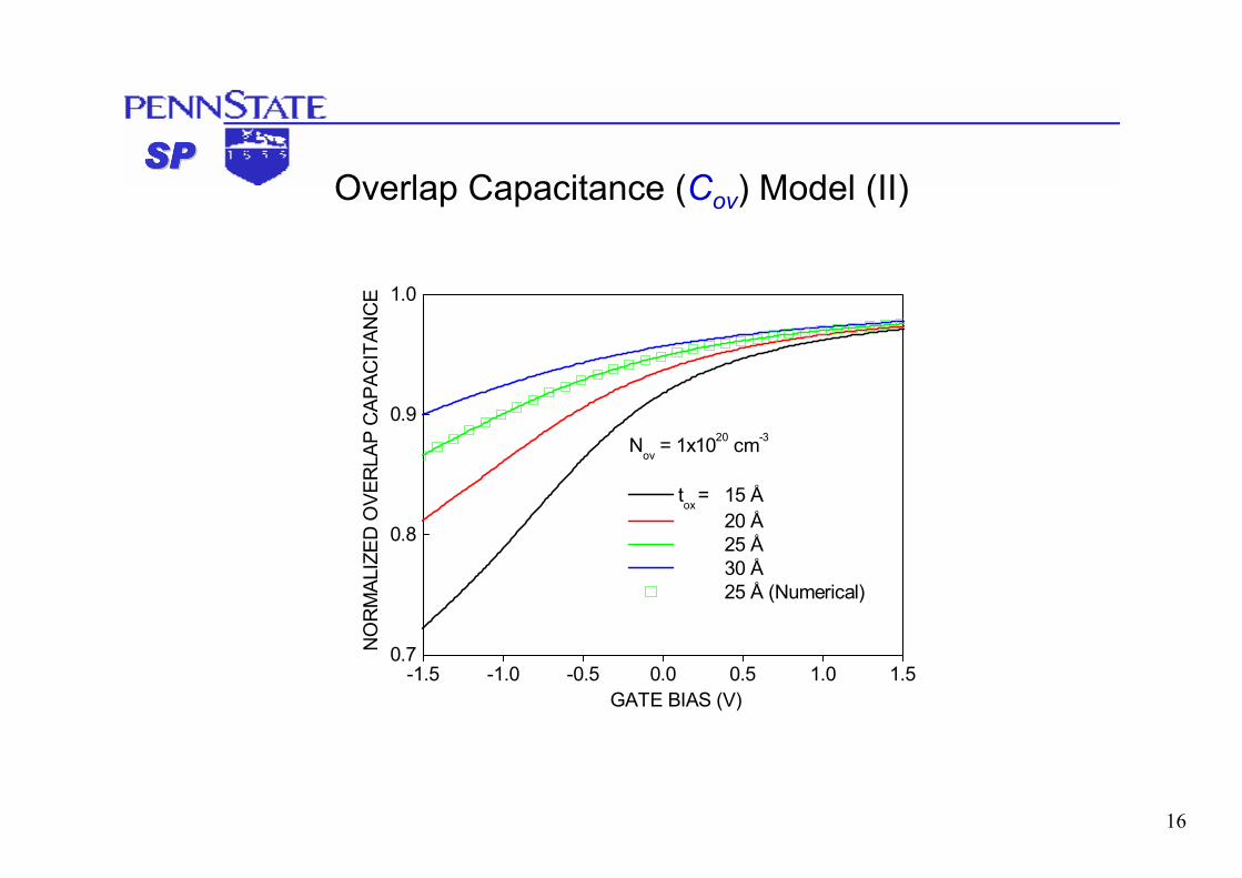
Overlap Capacitance (Cov) Model
• Lov/Lg↑ requires physically-based modeling of the overlap regions for scaled devices
• Conventional models either neglect the bias dependence of Cov or rely on the smoothing function to fit data
• SP models the overlap region as MOS capacitor
( )d d
ov ov oxov g ov
ov ov g
Q WL C V
C Q V
φ= −
=SS
GG n+Oxide
n+
Gate
Source/Drain
SPSPSPSPSPSPSPSP
16
Overlap Capacitance (Cov) Model (II)
-1.5 -1.0 -0.5 0.0 0.5 1.0 1.50.7
0.8
0.9
1.0
NO
RM
ALIZ
ED O
VER
LAP
CAP
ACIT
ANC
E
GATE BIAS (V)
Nov = 1x1020 cm-3
tox = 15 Å 20 Å 25 Å 30 Å 25 Å (Numerical)

SPSPSPSPSPSPSPSP
17
Gate Tunneling Current (Ig) Model
• Aggressive scaling of tox⇒ substantial Ig• Ig=Igc+Igsov+Igdov; the overlap component is
modeled physically• Igc=Igcs+Igcd; partition is achieved using a
physics-based approach• The physically correct carrier statistics
included in the Esaki-Tsu formula is implemented efficiently
• The same form of model and identical parameters are used in all the three components
• No scaling parameters are required to fit the data for different L
IIgcgc
IIggIIgsovgsov
IIgcdgcdIIgcsgcsDDSS
IIgdovgdov

SPSPSPSPSPSPSPSP
18
Gate Tunneling Current Model
-1.5 -1.0 -0.5 0.0 0.5 1.0 1.510-13
10-11
10-9
10-7
Vds = 0 V
W/L=10µm/10µm
Vbs = 0.3 V 0 0.3
Symbols: ExperimentLines: Model
I g (A)
Vgs (V)
W/L=10µm/0.17µm
-1.5 -1.0 -0.5 0.0 0.5 1.0 1.510-12
10-10
10-8
10-6
Vgs (V)

SPSPSPSPSPSPSPSP
19
Gate Tunneling Current Model
-1.0 -0.5 0.0 0.5 1.010-11
10-9
10-7
10-5
Vbs=0 V
W/L=70µm/10µm Symbols: ExperimentLines: Model
1.3
Vds=0.3 V
I g (A)
Vgs (V)

SPSPSPSPSPSPSPSP
20
Noise Sources – Circuit SimulationVdd
V cnt
out
outb
R0=350
M3 M2
M1 M0
L0=1nHL0=1nH L1=1nH
102 104 106 108
-210
-180
-150
-120
-90
-60
-30
0
20dB/dec
Noi
se S
pect
ral P
ower
Den
sity
(dBc
/Hz)
Frequency Offset (Hz)
total phase noise 1/f noise contribution thermal noise contribution
30dB/dec
Free-Running Oscillator Phase Noise Simulation
SP includes Φs-based models of 1/f noise, thermal noise and channel-induced gate noise. Single expression for spectral density is valid in all regions of operation

SPSPSPSPSPSPSPSP
21
Other SP features (not discussed in this presentation)
• Varactor modeling
• Quantum/Poly effects
• S-matrix (quasi-ballistic) version
• Physical model of inner-fringing capacitance
• Large-signal Φs-based NQS model (spline collocation method)

SPSPSPSPSPSPSPSP
22
Conclusions• Combination of Φs-based approach and symmetric linearization method allows to increase the physical content of the model without the usual increase in model complexity
• Analytical approximations for Φs (accurate within 1nV) allow one to eliminate the need for iterative loops and channel segmentation
• Rapid progress in the development of Φs-based models eliminates the historical advantages of simpler model structures (QI-based, VTH-based). Only Φs–based models lead to physical modeling of accumulation region.

SPSPSPSPSPSPSPSP
23
SP Publications
1. G. Gildenblat, N.D. Arora, R. Sung and P. Bendix, “Scalable Surface Potential Based Compact MOSFET Model”, Proc. 1997 International Semiconductor Device Research Symposium, pp .333-336, Charlottesville VA, Dec. 1997
2. G. Gildenblat, T. L. Chen and P. Bendix, “Analytical Approximation for the Perturbation of MOSFET Surface Potential by the Polysilicon Depletion Layer”, Electronics Letters, 35, 1974 (1999)
3. G. Gildenblat, T. L. Chen and P. Bendix, “Closed-form Approximation for the Perturbation of MOSFET Surface Potential by Quantum-Mechanical Effects”, Electronics Letters, 36, 1072 (2000)
4. T.L. Chen and G. Gildenblat, “Analytical Approximation for the MOSFET Surface Potential”, Solid-State Electronics, 45, 335-339 (2001)
5. T.L. Chen and G. Gildenblat, “Symmetric Bulk Charge Linearization of Charge-Sheet MOSFET Model”, Electronics Letters, 37, 791-793 (2001)
6. X. Gu and G. Gildenblat, “Charge-Sheet MOSFET Model with Surface Degeneracy and Freezeout”, Proc. 2001 International Semiconductor Device Research Symposium, pp.102-105, Washington, DC, Dec. 2001
7. G. Gildenblat, “ One-flux theory of a non-absorbing barrier”, J. Appl. Phys., 91, 9883 (2002)

SPSPSPSPSPSPSPSP
24
8. H. Wang and G. Gildenblat, “Scattering Matrix Based Compact MOSFET Model”, IEDM Tech, Digest, pp. 125-128, 2002
9. G. Gildenblat and T. L. Chen, “Overview of An Advanced Surface-Potential-Based MOSFET Model”, Technical Proc. of the Fifth International Conference on Modeling and Simulation of Microsystems, pp. 657-661, 2002 (invited)
10. X. Gu, G. Gildenblat, G. Workman, S. Veeraraghavan, S. Shapira and K. Stiles, “A Surface-Potential-Based Extrinsic Compact MOSFET Model”, Sixth International Conference on Modeling and Simulation of Microsystems, February 2003 (invited), in the Technical Proceedings of the 2003 Nanotechnology Conference, pp. 364-367
11. X. Gu, G. Gildenblat, G. Workman, S. Veeraraghavan, S. Shapira and K. Stiles, “A Surface-Potential-Based Compact Model of NMOSFET Gate Current”, Sixth International Conference on Modeling and Simulation of Microsystems, February 2003, in the Technical Proceedings of the 2003 Nanotechnology Conference, pp. 318-321
12. X. Cai, X. Gu, H. Wang and G. Gildenblat “Application of Genetic Algorithm to Compact MOSFET Model Parameter Extraction and Model Development”, Sixth International Conference on Modeling and Simulation of Microsystems, February 2003, in the Technical Proceedings of the 2003 Nanotechnology Conference, pp. 314-317
13. X. Gu, H. Wang, T.L. Chen and G. Gildenblat, “Substrate Current in Surface-Potential-Based Compact MOFET Models”, Sixth International Conference on Modeling and Simulation of Microsystems, February 2003, in the Technical Proceedings of the 2003 Nanotechnology Conference, pp. 310-312
SP Publications (continued)