sp14n02l6alcz - farnell · 2015-11-12 · for messrs : date : jan. 20th,2014 customer’s...
TRANSCRIPT
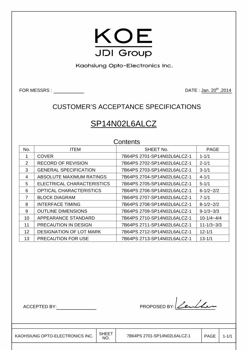
FOR MESSRS : DATE : Jan. 20th ,2014
CUSTOMER’S ACCEPTANCE SPECIFICATIONS
SP14N02L6ALCZ
Contents No. ITEM SHEET No. PAGE
1 COVER 7B64PS 2701-SP14N02L6ALCZ-1 1-1/1
2 RECORD OF REVISION 7B64PS 2702-SP14N02L6ALCZ-1 2-1/1
3 GENERAL SPECIFICATION 7B64PS 2703-SP14N02L6ALCZ-1 3-1/1
4 ABSOLUTE MAXIMUM RATINGS 7B64PS 2704-SP14N02L6ALCZ-1 4-1/1
5 ELECTRICAL CHARACTERISTICS 7B64PS 2705-SP14N02L6ALCZ-1 5-1/1
6 OPTICAL CHARACTERISTICS 7B64PS 2706-SP14N02L6ALCZ-1 6-1/2~2/2
7 BLOCK DIAGRAM 7B64PS 2707-SP14N02L6ALCZ-1 7-1/1
8 INTERFACE TIMING 7B64PS 2708-SP14N02L6ALCZ-1 8-1/2~2/2
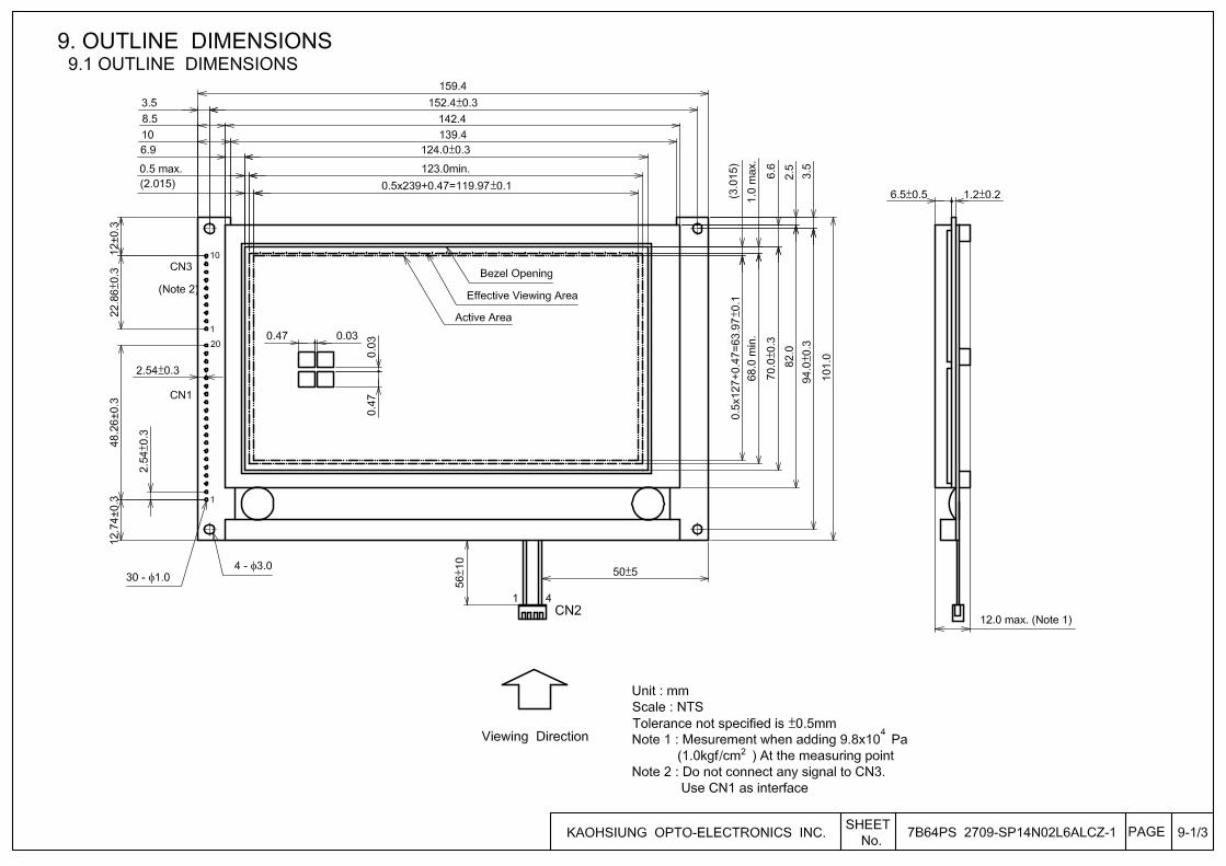
9 OUTLINE DIMENSIONS 7B64PS 2709-SP14N02L6ALCZ-1 9-1/3~3/3
10 APPEARANCE STANDARD 7B64PS 2710-SP14N02L6ALCZ-1 10-1/4~4/4
11 PRECAUTION IN DESIGN 7B64PS 2711-SP14N02L6ALCZ-1 11-1/3~3/3
12 DESIGNATION OF LOT MARK 7B64PS 2712-SP14N02L6ALCZ-1 12-1/1
13 PRECAUTION FOR USE 7B64PS 2713-SP14N02L6ALCZ-1 13-1/1
ACCEPTED BY: PROPOSED BY:
KAOHSIUNG OPTO-ELECTRONICS INC. SHEETNO. 7B64PS 2701-SP14N02L6ALCZ-1 PAGE 1-1/1
RECORD OF REVISION
DATE SHEET No. SUMMARY
KAOHSIUNG OPTO-ELECTRONICS INC. SHEETNO. 7B64PS 2702-SP14N02L6ALCZ-1 PAGE 2-1/1
3. GENERAL SPECIFICATIONS
(1) Part Name SP14N02L6ALCZ
(2) Module Size 159.4(W)mm x 101.0(H)mm x 12.0 (D)mm max.
(3) Dot Size 0.47(W)mm x 0.47(H)mm
(4) Dot Pitch 0.50(W)mm x 0.50(H)mm
(5) Number Of Dots 240(W) x 128(H)dots
(6) Duty 1/128
(7) LCD Type Film type black / white (Negative type)
The upper polarizer is anti-glare type.
(Hardness.3H)
The bottom polarizer is transmissive type.
(8) Viewing Direction 6 O’clock
(9) Backlight Light-Emitting Diode
(10) LED Lifetime 50k hrs.
KAOHSIUNG OPTO-ELECTRONICS INC. SHEETNO. 7B64PS 2703-SP14N02L6ALCZ-1 PAGE 3-1/1
4. ABSOLUTE MAXIMUM RATINGS 4.1 Electrical Absolute Maximum Ratings. VSS = 0V : Standard
ITEM SYMBOL MIN. MAX. UNIT COMMENT Power Supply For Logic VDD-VSS 0 6.5 V Power Supply For LC Drive VDD-VEE 0 20.5 V Input Voltage Vi -0.3 VDD+0.3 V Input Current Ii 0 1 A Static Electricity - - - - Note 1
Note 1: Make certains you are grounded when handling LCM. 4.2 Environmental Absolute Maximum Ratings
ITEM OPERATING STORAGE
COMMENT MIN. MAX. MIN. MAX.
Ambient Temperature 0℃ 50℃ -20℃ 60℃ Note 2,3 Humidity Note 1 Note 1 Without Condensation
Vibration - 4.9m/s2
(0. 5G)-
19.6m/s2
(2G) Note 5
Note 4
Shock - 29.4m/s2
(3 G) -
490.0m/s2
(50 G) XYZ Directions
Corrosive Gas Not Acceptable Not Acceptable Note 1: Ta≦40℃ : 85%RH max. Ta>40℃ : Absolute humidity must be lower than the humidity of 85%RH at 40℃ Note 2: Ta at -20℃ ------< 48h, at 60℃ ------< 168h.
Note 3: The maximum rating is defined as above based on the chamber temperature, which might
be different from ambient temperature after assembling the panel into the application.
Moreover some temperature-related phenomenon as below needed to be noticed:
- Background color, contrast and response time would be different in temperatures other than 25℃.
- Operating under high temperature will shorten LED lifetime. Note 4: 5Hz~100Hz (Except Resonance Frequency) Note 5: This module should be operated normally after finishing the test.
KAOHSIUNG OPTO-ELECTRONICS INC. SHEETNO. 7B64PS 2704-SP14N02L6ALCZ-1 PAGE 4-1/1
5. ELECTRICAL CHARACTERISTICS 5.1 ELECTRICAL CHARACTERISTICS
ITEM SYMBOL CONDITION MIN. TYP. MAX. UNITPower Supply Voltage For Logic VDD-VSS - 4.75 5.0 5.25 V
LC driver Circuit Power Supply Voltage
VEE-VSS - -15.5 -15.0 -14.5 V
Input Voltage VI H LEVEL 0.8VDD - VDD V
L LEVEL 0 - 0.2VDD V Power Supply Current For Logic Note 1
IDD VDD-VSS=5.0V - 11.7 14.0 mA
Power Supply Current For LCD Note 1
IEE VDD-VSS=5.0V - 2.5 4.0 mA
Recommended LC Driving Voltage Note 2
VDD-V0 Ta= 0℃ , = 0° - 16.9 - V Ta=25℃ , =0° - 15.8 - V Ta=50℃ , =0° - 15.2 - V
Note 1: VDD-V0=15.8V , Ta=25℃ Note 2: Recommended LC driving voltage may fluctuate about ±1.0V by each module. Test pattern is all “Q”. 5.2 ELECTRICAL CHARACTERISTICS OF BACKLIGHT
ITEM SYMBOL MIN. TYP. MAX. UNIT NOTE
LED Input Voltage VLED - 5 5.7 V Note 1
LED Forward Current ILED - 144 - mA
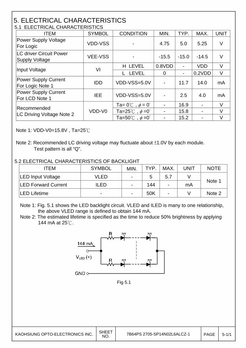
LED Lifetime - - 50K - V Note 2 Note 1: Fig. 5.1 shows the LED backlight circuit. VLED and ILED is many to one relationship, the above VLED range is defined to obtain 144 mA. Note 2: The estimated lifetime is specified as the time to reduce 50% brightness by applying 144 mA at 25℃.
KAOHSIUNG OPTO-ELECTRONICS INC. SHEETNO. 7B64PS 2705-SP14N02L6ALCZ-1 PAGE 5-1/1
Fig 5.1
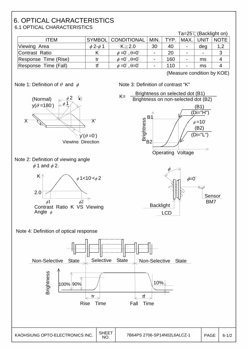
6. OPTICAL CHARACTERISTICS 6.1 OPTICAL CHARACTERISTICS Ta=25℃(Backlight on)
ITEM SYMBOL CONDITIONAL MIN. TYP. MAX. UNIT NOTEViewing Area 2- 1 K≧2.0 30 40 - deg 1,2 Contrast Ratio K =0° , =0° - 20 - - 3 Response Time (Rise) tr =0° , =0° - 160 - ms 4 Response Time (Fall) tf =0° , =0° - 110 - ms 4
Note 1: Definition of and Note 3: Definition of contrast “K”
Note 2: Definition of viewing angle
1 and 2.
Note 4: Definition of optical response
Operating Voltage
B1
B2
(B1) (Di="H")
(B2) (Di="L")
Brig
htn
ess
=10°
X
2
Viewing Direction
(Normal) y( =180°) 1
X’
y’( =0°)
Backlight
LCD
Sensor
=0°
K
2.0
Contrast Ratio K VS Viewing Angle
1<10°< 2
1 2
Non-Selective State
100% 90% 10%
tr tf
Rise Time Fall Time
Selective State Non-Selective State
Brig
htn
ess
(Measure condition by KOE)
Brightness on selected dot (B1) Brightness on non-selected dot (B2)
K=
BM7
KAOHSIUNG OPTO-ELECTRONICS INC. SHEETNO. 7B64PS 2706-SP14N02L6ALCZ-1 PAGE 6-1/2
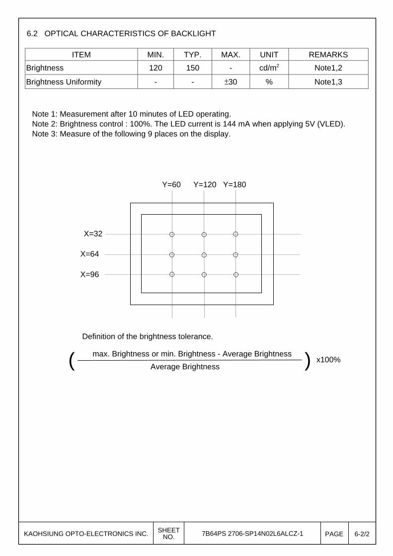
6.2 OPTICAL CHARACTERISTICS OF BACKLIGHT
ITEM MIN. TYP. MAX. UNIT REMARKS
Brightness 120 150 - cd/m2 Note1,2
Brightness Uniformity - - ±30 % Note1,3
Note 1: Measurement after 10 minutes of LED operating. Note 2: Brightness control : 100%. The LED current is 144 mA when applying 5V (VLED). Note 3: Measure of the following 9 places on the display.
Definition of the brightness tolerance.
Y=180Y=120Y=60
X=32
X=64
X=96
KAOHSIUNG OPTO-ELECTRONICS INC. SHEETNO. 7B64PS 2706-SP14N02L6ALCZ-1 PAGE 6-2/2
max. Brightness or min. Brightness - Average Brightnessx100% ( ) Average Brightness
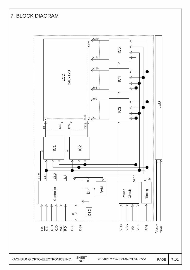
7. BLOCK DIAGRAM
KAOHSIUNG OPTO-ELECTRONICS INC. SHEETNO. 7B64PS 2707-SP14N02L6ALCZ-1 PAGE 7-1/1
VLE
D+
VLE
D-
Con
trol
ler
13
8
D1
CL2
CL1
FLM
IC1
IC2
RA
M
Pow
er
Circ
uit
Tim
ing
M’
VLC
D
IC3
IC4
IC5
LED
LCD
240x
128
X1
X64
X65
X12
8
X12
8
Y1
Y24
0
Y240
VE
E
V0
VD
D
DB
0
D
B7
RD
WR
C
/D
RE
T
CE
8 OS
C
VS
S
P/N
F/S
X
1
Y161
Y160
Y81
Y80
Y1
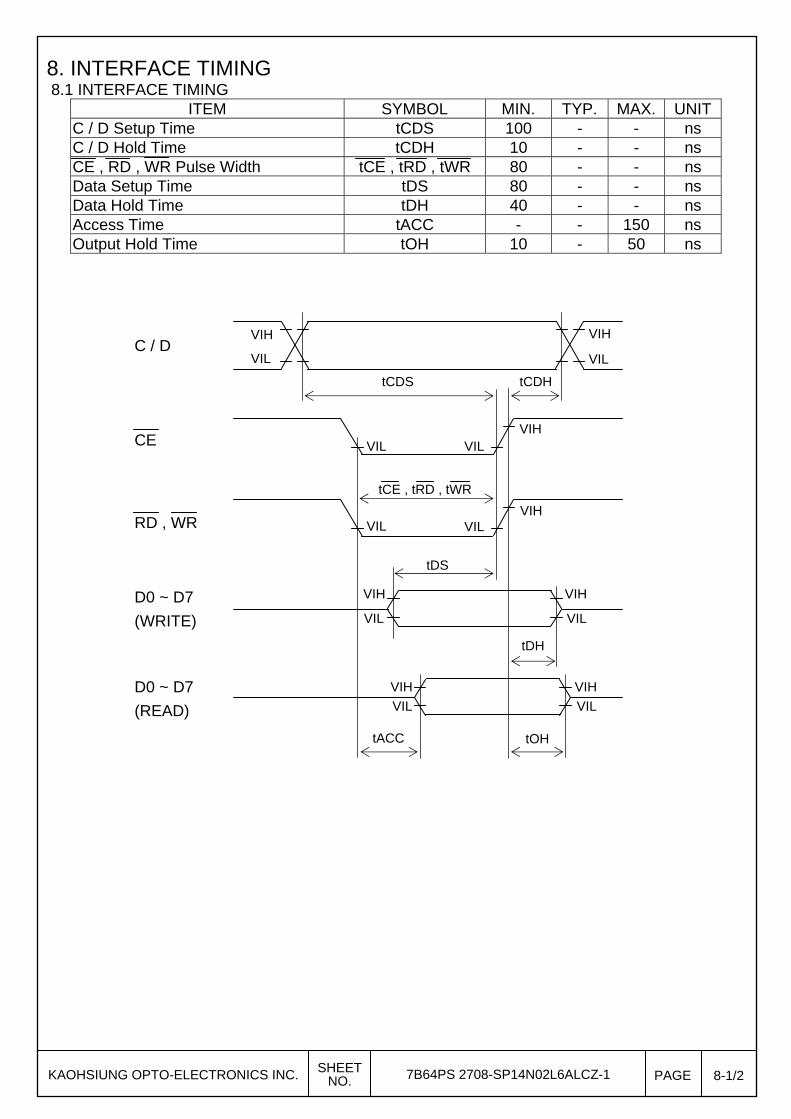
8. INTERFACE TIMING 8.1 INTERFACE TIMING
ITEM SYMBOL MIN. TYP. MAX. UNITC / D Setup Time tCDS 100 - - ns C / D Hold Time tCDH 10 - - ns CE , RD , WR Pulse Width tCE , tRD , tWR 80 - - ns Data Setup Time tDS 80 - - ns Data Hold Time tDH 40 - - ns Access Time tACC - - 150 ns Output Hold Time tOH 10 - 50 ns
VIH
VIL C / D
VIH
VIL
tCDS tCDH
VIL VIL VIH
VIHVIL VIL
tDS
VIH VIH
VIL VIL
tDH
VIH
VIL
VIH
VIL
tACC tOH
tCE , tRD , tWR
CE
RD , WR
D0 ~ D7
(WRITE)
D0 ~ D7
(READ)
KAOHSIUNG OPTO-ELECTRONICS INC. SHEETNO. 7B64PS 2708-SP14N02L6ALCZ-1 PAGE 8-1/2
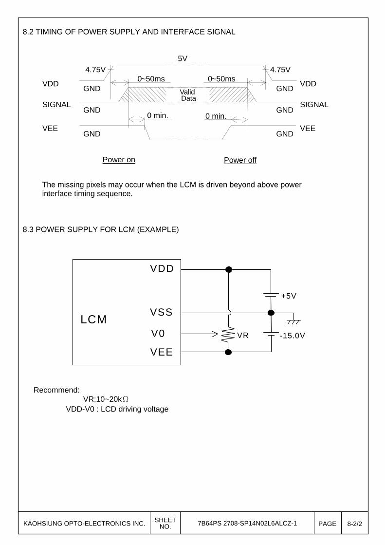
8.2 TIMING OF POWER SUPPLY AND INTERFACE SIGNAL
The missing pixels may occur when the LCM is driven beyond above power interface timing sequence. 8.3 POWER SUPPLY FOR LCM (EXAMPLE)
Recommend: VR:10~20kΩ VDD-V0 : LCD driving voltage
4.75V
VDD
SIGNAL
VEE
GND
GND
GND
0 ~50ms
ValidData
0 min. 0 min.
4.75V
GND
GND
GND
VDD
SIGNAL
VEE
Power on Power off
5V
0~50ms
LCM
VDD
VSS
VEE
+5V
-15.0V VRV0
KAOHSIUNG OPTO-ELECTRONICS INC. SHEETNO. 7B64PS 2708-SP14N02L6ALCZ-1 PAGE 8-2/2
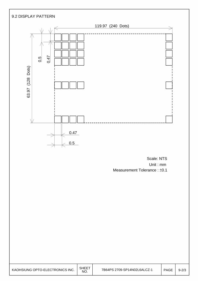
9.2 DISPLAY PATTERN
119.97 (240 Dots)
63.9
7 (
128
Dot
s)
0.5
0.47
0.5
0.47
Scale: NTS
Unit : mm Measurement Tolerance : ±0.1
KAOHSIUNG OPTO-ELECTRONICS INC. SHEETNO. 7B64PS 2709-SP14N02L6ALCZ-1 PAGE 9-2/3
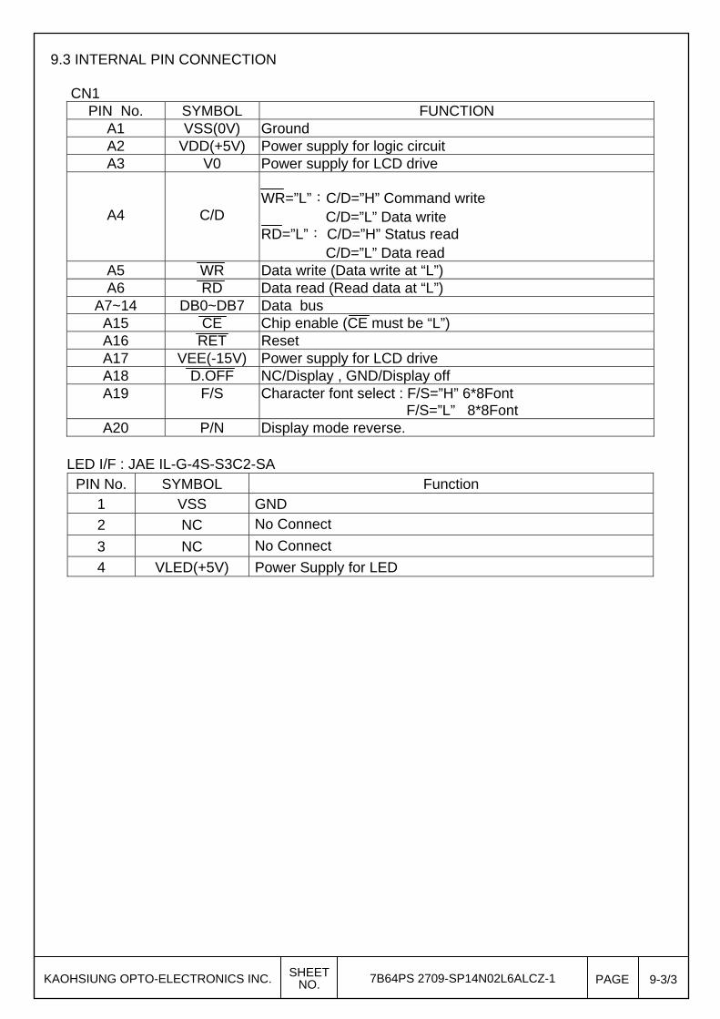
9.3 INTERNAL PIN CONNECTION CN1
PIN No. SYMBOL FUNCTION A1 VSS(0V) Ground A2 VDD(+5V) Power supply for logic circuit A3 V0 Power supply for LCD drive
A4
C/D
WR=”L”:C/D=”H” Command write C/D=”L” Data write RD=”L”: C/D=”H” Status read C/D=”L” Data read
A5 WR Data write (Data write at “L”) A6 RD Data read (Read data at “L”)
A7~14 DB0~DB7 Data bus A15 CE Chip enable (CE must be “L”) A16 RET Reset A17 VEE(-15V) Power supply for LCD drive A18 D.OFF NC/Display , GND/Display off A19 F/S Character font select : F/S=”H” 6*8Font
F/S=”L” 8*8Font A20 P/N Display mode reverse.
LED I/F : JAE IL-G-4S-S3C2-SA
PIN No. SYMBOL Function 1 VSS GND
2 NC No Connect
3 NC No Connect
4 VLED(+5V) Power Supply for LED
KAOHSIUNG OPTO-ELECTRONICS INC. SHEETNO. 7B64PS 2709-SP14N02L6ALCZ-1 PAGE 9-3/3
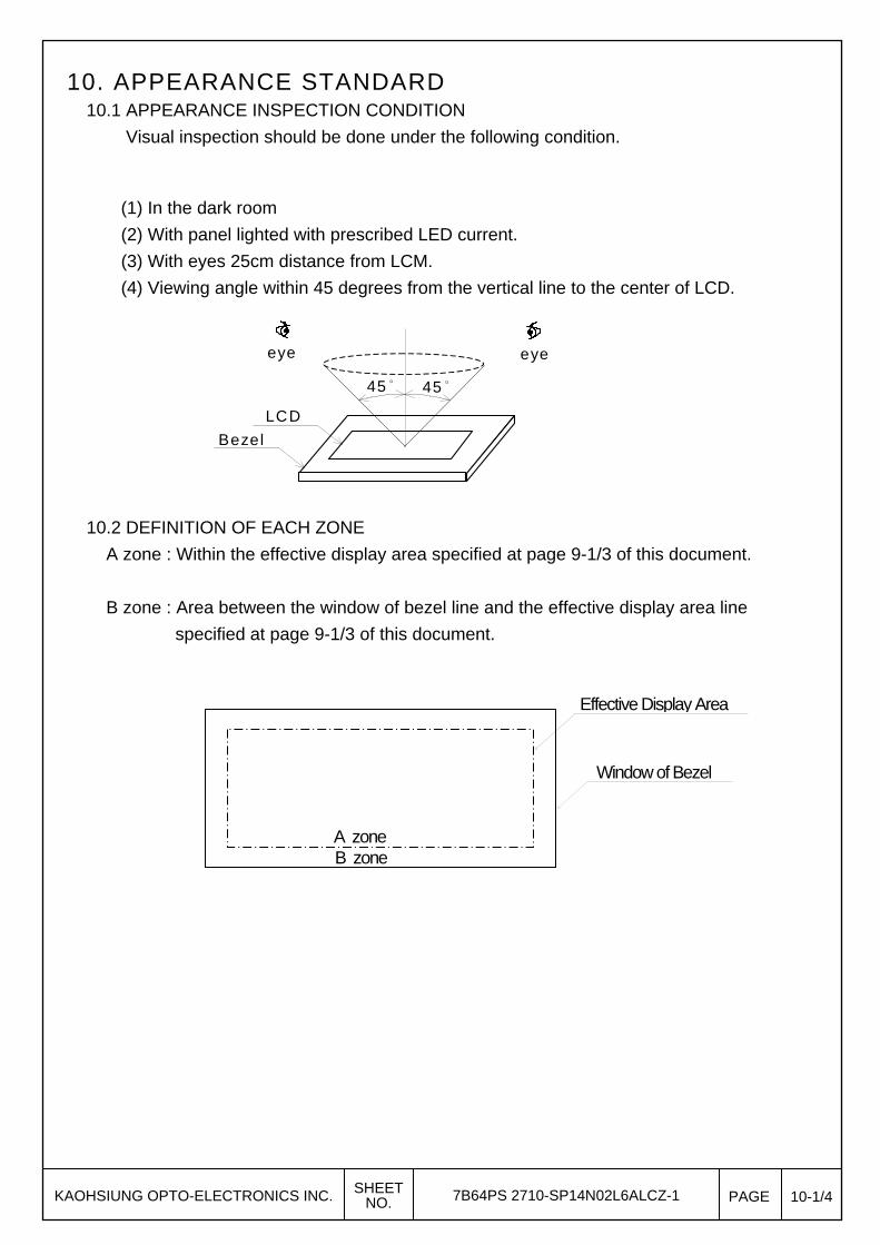
10. APPEARANCE STANDARD 10.1 APPEARANCE INSPECTION CONDITION
Visual inspection should be done under the following condition.
(1) In the dark room
(2) With panel lighted with prescribed LED current.
(3) With eyes 25cm distance from LCM.
(4) Viewing angle within 45 degrees from the vertical line to the center of LCD.
10.2 DEFINITION OF EACH ZONE
A zone : Within the effective display area specified at page 9-1/3 of this document.
B zone : Area between the window of bezel line and the effective display area line
specified at page 9-1/3 of this document.
45° 45°
LCD
Bezel
eye eye
Effective Display Area
Window of Bezel
A zoneB zone
KAOHSIUNG OPTO-ELECTRONICS INC. SHEETNO. 7B64PS 2710-SP14N02L6ALCZ-1 PAGE 10-1/4
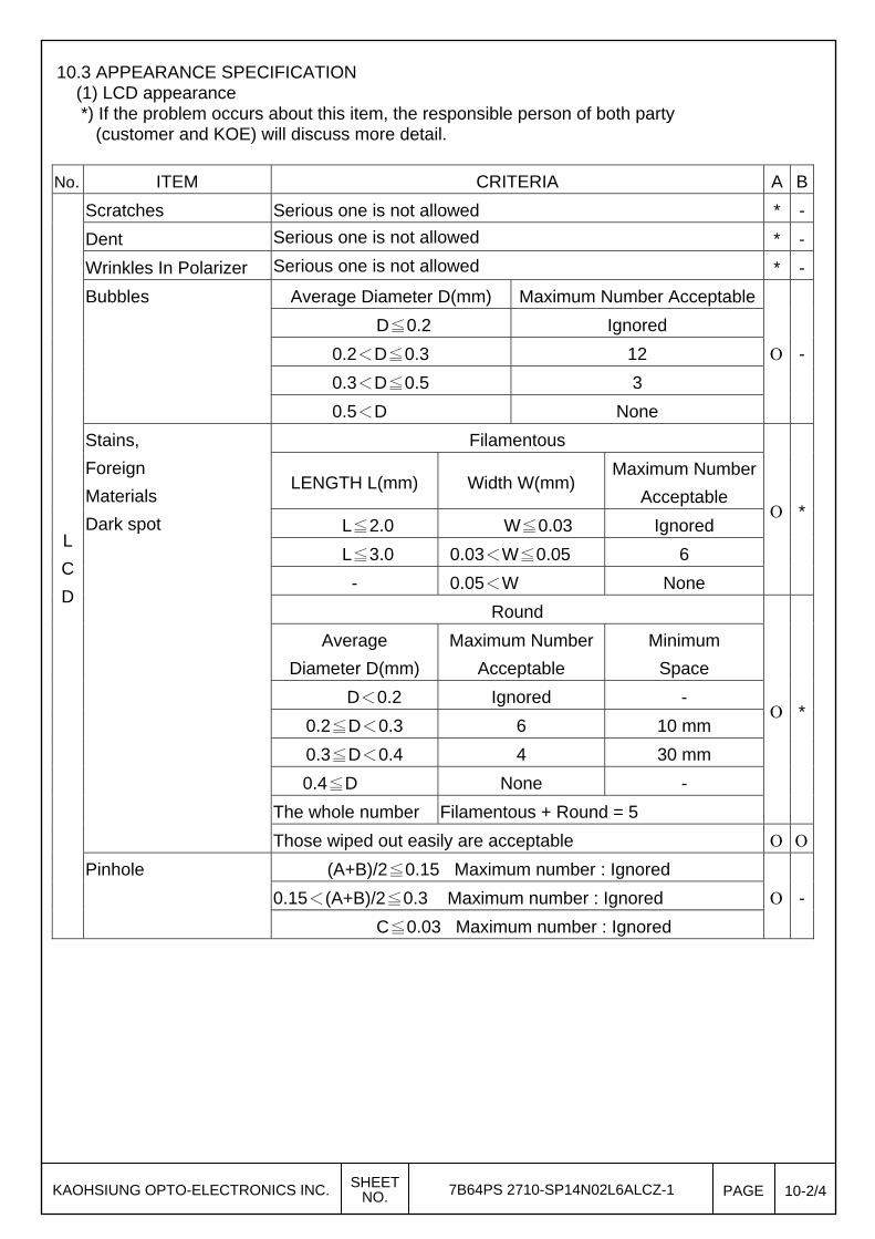
10.3 APPEARANCE SPECIFICATION (1) LCD appearance *) If the problem occurs about this item, the responsible person of both party (customer and KOE) will discuss more detail.
No. ITEM CRITERIA A B
L
C
D
Scratches Serious one is not allowed * -
Dent Serious one is not allowed * -
Wrinkles In Polarizer Serious one is not allowed * -
Bubbles Average Diameter D(mm) Maximum Number Acceptable
-
D≦0.2 Ignored
0.2<D≦0.3 12
0.3<D≦0.5 3
0.5<D None
Stains,
Foreign
Materials
Dark spot
Filamentous
*
LENGTH L(mm) Width W(mm) Maximum Number
Acceptable
L≦2.0 W≦0.03 Ignored
L≦3.0 0.03<W≦0.05 6
- 0.05<W None
Round
*
Average
Diameter D(mm)
Maximum Number
Acceptable
Minimum
Space
D<0.2 Ignored -
0.2≦D<0.3 6 10 mm
0.3≦D<0.4 4 30 mm
0.4≦D None -
The whole number Filamentous + Round = 5
Those wiped out easily are acceptable
Pinhole (A+B)/2≦0.15 Maximum number : Ignored
-0.15<(A+B)/2≦0.3 Maximum number : Ignored
C≦0.03 Maximum number : Ignored
KAOHSIUNG OPTO-ELECTRONICS INC. SHEETNO. 7B64PS 2710-SP14N02L6ALCZ-1 PAGE 10-2/4
No. ITEM CRITERIA A B
L
C
D
Contrast
Irregularity
(Spot)
Average
Diameter
D(mm)
Maximum
Number
Acceptable
Minimum
Space
- D≦0.25 Ignored -
0.25<D≦0.35 10 20mm
0.35<D≦0.5 4 20mm
0.5 <D None -
Contrast
Irregularity
( A Pair of
Scratch)
Width
W(mm)
Length
L(mm)
Maximum
Number
Acceptable
Minimum
Space
- W≦0.25 L≦1.2 2 20mm
W≦0.2 L≦1.5 3 20mm
W≦0.15 L≦2.0 3 20mm
W≦0.1 L≦3.0 4 20mm
The whole number 6
KAOHSIUNG OPTO-ELECTRONICS INC. SHEETNO. 7B64PS 2710-SP14N02L6ALCZ-1 PAGE 10-3/4
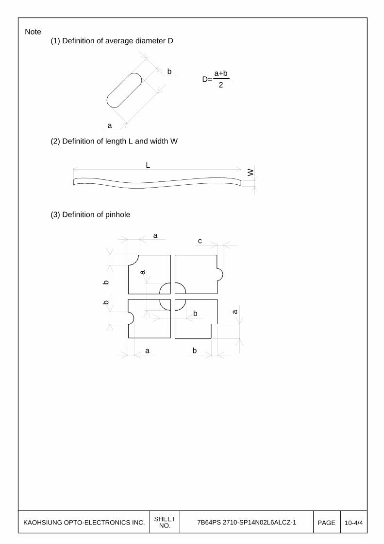
Note (1) Definition of average diameter D
(2) Definition of length L and width W
(3) Definition of pinhole
b
a
D=a+b
2
c
b
b
b b
a
W L
a
a
a
KAOHSIUNG OPTO-ELECTRONICS INC. SHEETNO. 7B64PS 2710-SP14N02L6ALCZ-1 PAGE 10-4/4
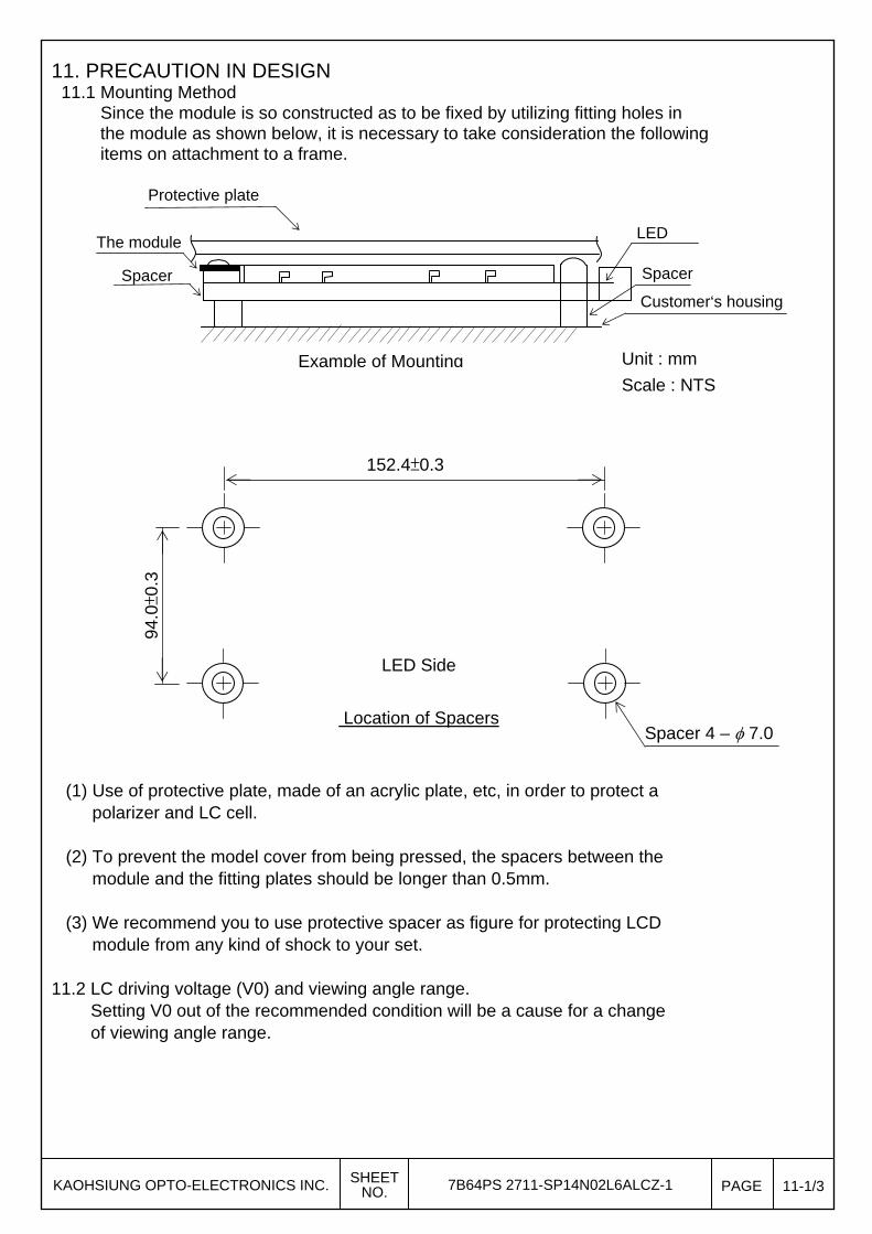
11. PRECAUTION IN DESIGN 11.1 Mounting Method Since the module is so constructed as to be fixed by utilizing fitting holes in the module as shown below, it is necessary to take consideration the following items on attachment to a frame.
(1) Use of protective plate, made of an acrylic plate, etc, in order to protect a polarizer and LC cell.
(2) To prevent the model cover from being pressed, the spacers between the module and the fitting plates should be longer than 0.5mm.
(3) We recommend you to use protective spacer as figure for protecting LCD module from any kind of shock to your set.
11.2 LC driving voltage (V0) and viewing angle range. Setting V0 out of the recommended condition will be a cause for a change of viewing angle range.
Example of Mounting Unit : mm
Scale : NTS
Spacer
The module
Customer‘s housing
Spacer
Protective plate
LED
LED Side
Location of Spacers Spacer 4 – 7.0
152.4±0.3
94.0±0.
3
KAOHSIUNG OPTO-ELECTRONICS INC. SHEETNO. 7B64PS 2711-SP14N02L6ALCZ-1 PAGE 11-1/3
11.3 CAUTION AGAINST STATIC CHARGE As this module is provided with C-MOS LSI, the care to take such a precaution as to grounding the operator‘s body is required when handling it. 11.4 POWER ON SEQUENCE Input signals should not be applied to LCD module before power supply voltage is applied and reaches to specified voltage (5±0.25V). If above sequence is not kept, C-MOS LSIS of LCD modules may be damaged due to latch up problem. 11.5 PACKAGING (1) No. leaving products is preferable in the place of high humidity for a long period of time. for their storage in the place where temperature is 35℃ or higher, special care to prevent them from high humidity is required. A combination of high temperature and high humidity may cause them polarization degradation as well as bubble generation and polarizer peel-off. Please keep the temperature and humidity within the specified range for use and storing. (2) Since upper polarizers and lower aluminum plates tend to be easily damaged, they should be handled with full care so as not to get them touched, pushed or rubbed by a piece of glass, tweezers and anything else which are harder than a pencil lead 3h. (3) As the adhesives used for adhering upper/lower polarizers and aluminum plates are made of organic substances which will be deteriorated by a chemical reaction with such chemicals as acetone, toluene ethanol and isopropyl alcohol. The following solvents are recommended for use: normal hexane please contact us when it is necessary for you to use chemicals other than the above. (4) Lightly wipe to clean the dirty surface with absorbent cotton waste or other soft material like chamois, soaked in the chemicals recommended without scrubbing it hardly. To prevent the display surface from damage and keep the appearance in good state, it is sufficient, in general, to wipe it with absorbent cotton. (5) Immediately wipe off saliva or water drop attached on the display area because its long period adherence may cause deformation or faded color on the spot. (6) Fogy dew deposited on the surface and contact terminals due to coldness will be a cause for polarizer damage, stain and dirt on product. When necessary to take out the products from some place at low temperature for test, etc. It is required for them to be warmed up in a container once at the temperature higher than that of room.
KAOHSIUNG OPTO-ELECTRONICS INC. SHEETNO. 7B64PS 2711-SP14N02L6ALCZ-1 PAGE 11-2/3
(7) Touching the display area and contact terminals with bare hands and contaminating them are prohibited, because the stain on the display area and poor insulation between terminals are often caused by being touched by bare hands. (There are some cosmetics detrimental to polarizers.) (8) In general the quality of glass is fragile so that it tends to be cracked or chipped in handling, specially on its periphery please be careful not give it sharp shock caused by dropping down, ect. 11.6 CAUTION FOR OPERATION (1) It is an indispensable condition to drive LCD’s within the specified voltage limit since the higher voltage than the limit causes the shorter LCD life. An electrochemical reaction due to direct current causes LCD’s undesirable deterioration, so that the use of direct current driver should be avoided. (2) Response time will be extremely delayed at lower temperature than the operating temperature range and on the other hand at higher temperature LCD’s show dark blue color in them. However those phenomena do not mean inpediment or out of order with LCD’s which will come back in the specified operating temperature range. (3) If the display area is pushed hard during operation, some font will be abnormally displayed but it resumes normal condition after turning off once. (4) A slight dew depositing on terminals is a cause for electrochemical reaction resulting in terminal open circuit. Usage under the relative condition of 40℃ 50%RH less is required. 11.7 STORAGE In case of storing for a long period of time (for instance, for years) for the purpose of replacement use, the following ways are recommended. (1) Storage in a polyethylene bag with the opening sealed so as not to enter fresh air outside in it, and with no desiccant. (2) The placing in a dark room where neither exposure to direct sunlight nor light is, keeping temperature in the range from 0℃ to 35℃. (3) Storing with no touch on polarizer surface by anything else. (It is recommended to stone them as they have been contained in the inner container at the time of delivery from us.) 11.8 SAFETY (1) It is recommendable to crash damaged or unnecessary LCD’s into pieces and wash off liquid crystal by either of solvents such as acetone and ethanol, which shoud be burned up later. (2) When any liquid leaked out of a damaged glass gall comes in contact with your hands, please wash it off well with soap and water.
KAOHSIUNG OPTO-ELECTRONICS INC. SHEETNO. 7B64PS 2711-SP14N02L6ALCZ-1 PAGE 11-3/3
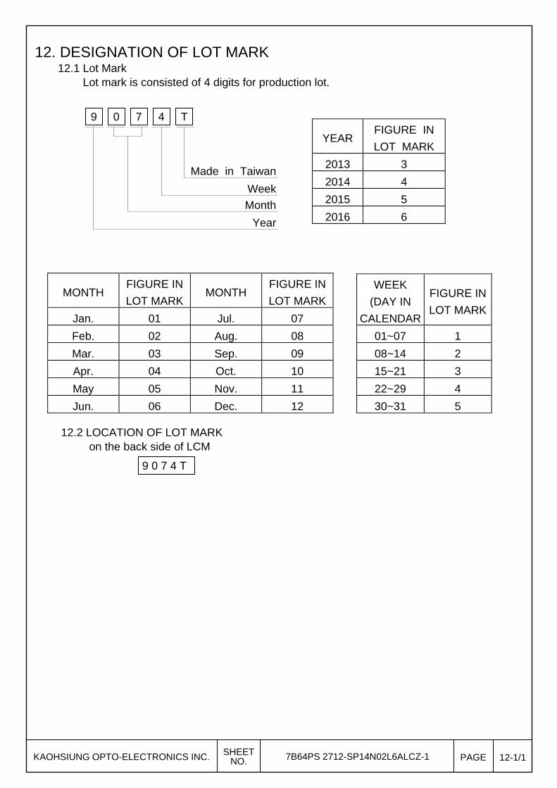
12. DESIGNATION OF LOT MARK 12.1 Lot Mark Lot mark is consisted of 4 digits for production lot. 12.2 LOCATION OF LOT MARK on the back side of LCM
WEEK
(DAY IN
CALENDAR
FIGURE IN
LOT MARK
01~07 1
08~14 2
15~21 3
22~29 4
30~31 5
MONTH FIGURE IN
LOT MARK MONTH
FIGURE IN
LOT MARK
Jan. 01 Jul. 07
Feb. 02 Aug. 08
Mar. 03 Sep. 09
Apr. 04 Oct. 10
May 05 Nov. 11
Jun. 06 Dec. 12
47 0 9
YEAR FIGURE IN
LOT MARK
2013 3
2014 4
2015 5
2016 6
T
Made in Taiwan
Week
Month
Year
9 0 7 4 T
KAOHSIUNG OPTO-ELECTRONICS INC. SHEETNO. 7B64PS 2712-SP14N02L6ALCZ-1 PAGE 12-1/1
13. PRECAUTION FOR USE (1) A limit sample should be provided by the both parties on an occasion when the both parties agreed its necessity. Judgement by a limit sample shall take effect after the limit sample has been eatablished and confirmed by the both parties. (2) On the following occasions, the handling of the problem should be decided through discussion and agreement between responsible persons of the both parties. (1) When a question is arisen in the specifications. (2) When a new problem is arisen which is not specified in this specifications. (3) When an inspection specifications change or operating condition change in customer is reported to KOE, and some problem is arisen in this specification due to the change. (4) When a new problem is arisen at the customer’s operating set for sample evaluation in the customer site. (3) Regarding the treatment for maintenance and repairing, both parties will disscuss it in six months later after latest delivery of this product. The precaution that should be observed when handling LCM have been explaind above. If any points are unclear of if you have any requests, please contact KOE.
KAOHSIUNG OPTO-ELECTRONICS INC. SHEETNO. 7B64PS 2713-SP14N02L6ALCZ-1 PAGE 13-1/1