spc57xx adc device - st.com · 4.1 gain calibration procedure ... saradc block diagram ... soc...
TRANSCRIPT
December 2013 DocID025610 Rev 1 1/33
AN4413Application note
SPC57xx ADC device
IntroductionThe aim of this document is to clarify the usage and features compared to the SPC57xx ‘s ADC, in order to help the user to find the best configuration to optimize the device use, in term of quality/precision of the sampled signals.
Document is intended as a guideline for the SARADC and SDADC features.
www.st.com
Contents AN4413
2/33 DocID025610 Rev 1
Contents
1 SAR ADC characteristics . . . . . . . . . . . . . . . . . . . . . . . . . . . . . . . . . . . . . 6
1.1 Features . . . . . . . . . . . . . . . . . . . . . . . . . . . . . . . . . . . . . . . . . . . . . . . . . . . 7
1.2 Considerations on the input impedance of the signal source . . . . . . . . . . . 8
1.3 Conversion timings . . . . . . . . . . . . . . . . . . . . . . . . . . . . . . . . . . . . . . . . . . 10
1.4 SARADC: constrain and timing . . . . . . . . . . . . . . . . . . . . . . . . . . . . . . . . .11
2 SD ADC characteristics . . . . . . . . . . . . . . . . . . . . . . . . . . . . . . . . . . . . . 13
2.1 Features . . . . . . . . . . . . . . . . . . . . . . . . . . . . . . . . . . . . . . . . . . . . . . . . . . 14
2.2 Considerations on the input impedance of the signal source . . . . . . . . . . 14
2.3 SDADC and DMA . . . . . . . . . . . . . . . . . . . . . . . . . . . . . . . . . . . . . . . . . . 15
2.4 SDADC conversion timing . . . . . . . . . . . . . . . . . . . . . . . . . . . . . . . . . . . . 15
2.5 Data conversion step . . . . . . . . . . . . . . . . . . . . . . . . . . . . . . . . . . . . . . . . 17
2.6 Data conversion timing . . . . . . . . . . . . . . . . . . . . . . . . . . . . . . . . . . . . . . . 17
2.7 SDADC calibration . . . . . . . . . . . . . . . . . . . . . . . . . . . . . . . . . . . . . . . . . 18
2.8 Offset calibration procedure . . . . . . . . . . . . . . . . . . . . . . . . . . . . . . . . . . . 19
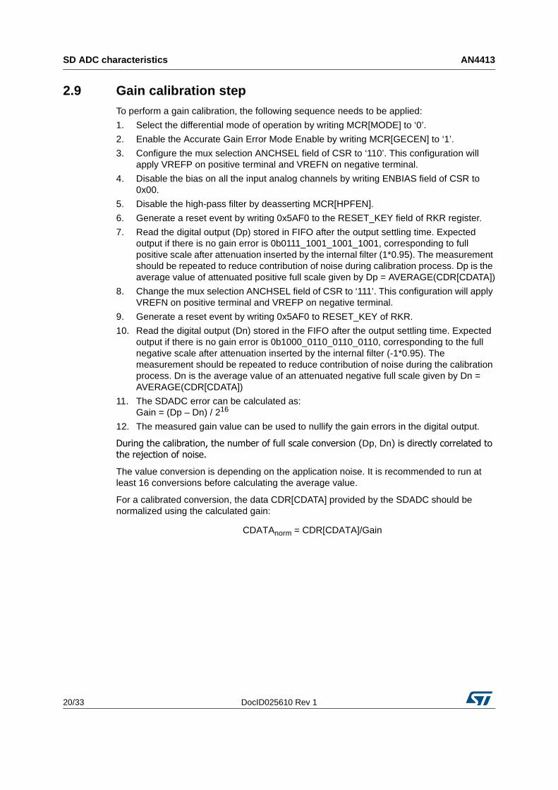
2.9 Gain calibration step . . . . . . . . . . . . . . . . . . . . . . . . . . . . . . . . . . . . . . . . . 20
3 SAR vs SD . . . . . . . . . . . . . . . . . . . . . . . . . . . . . . . . . . . . . . . . . . . . . . . . 21
4 ADC: automotive use cases . . . . . . . . . . . . . . . . . . . . . . . . . . . . . . . . . . 22
Appendix A . . . . . . . . . . . . . . . . . . . . . . . . . . . . . . . . . . . . . . . . . . . . . . . . . . . . . . . 23
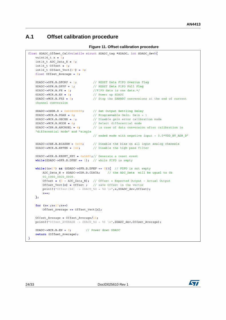
A.1 Offset calibration procedure . . . . . . . . . . . . . . . . . . . . . . . . . . . . . . . . . . . 24
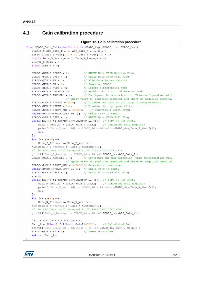
4.1 Gain calibration procedure . . . . . . . . . . . . . . . . . . . . . . . . . . . . . . . . . . . . 25
4.2 SDADC_0 CH2 setting . . . . . . . . . . . . . . . . . . . . . . . . . . . . . . . . . . . . . . . 26
4.3 Test N.1: SDADC0_ CH2 acquisition . . . . . . . . . . . . . . . . . . . . . . . . . . . 26
4.3.1 CH2 acquisition values: 5V . . . . . . . . . . . . . . . . . . . . . . . . . . . . . . . . . . 27
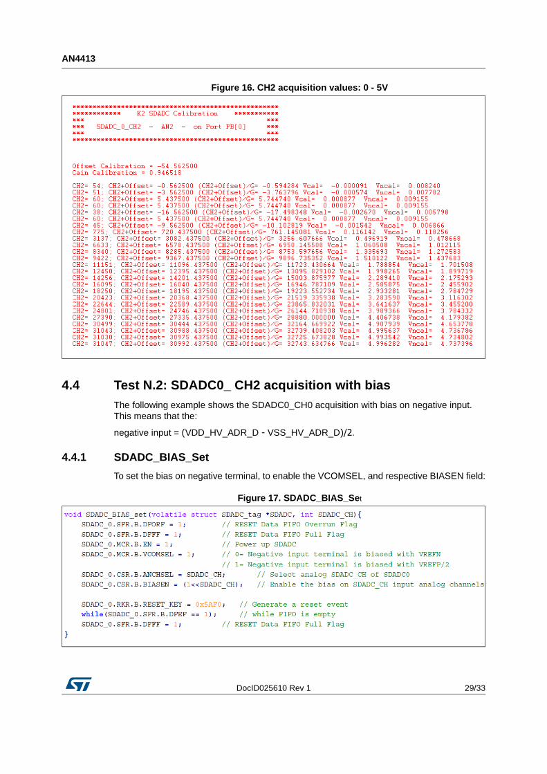
4.3.2 CH2 acquisition values: 0 - 5V . . . . . . . . . . . . . . . . . . . . . . . . . . . . . . . . 28
4.4 Test N.2: SDADC0_ CH2 acquisition with bias . . . . . . . . . . . . . . . . . . . . 29
4.4.1 SDADC_BIAS_Set . . . . . . . . . . . . . . . . . . . . . . . . . . . . . . . . . . . . . . . . . 29
4.4.2 CH2 acquisition values: -2.5 V - +2.5 V . . . . . . . . . . . . . . . . . . . . . . . . . 30
Appendix B Other information. . . . . . . . . . . . . . . . . . . . . . . . . . . . . . . . . . . . . . . . 31

DocID025610 Rev 1 3/33
AN4413 Contents
3
B.1 Reference documents . . . . . . . . . . . . . . . . . . . . . . . . . . . . . . . . . . . . . . . . 31
B.2 Acronyms . . . . . . . . . . . . . . . . . . . . . . . . . . . . . . . . . . . . . . . . . . . . . . . . . 31
Revision history . . . . . . . . . . . . . . . . . . . . . . . . . . . . . . . . . . . . . . . . . . . . . . . . . . . . 32
List of tables AN4413
4/33 DocID025610 Rev 1
List of tables
Table 1. 10 bit SARADC timing . . . . . . . . . . . . . . . . . . . . . . . . . . . . . . . . . . . . . . . . . . . . . . . . . . . . 11Table 2. SAR ADC vs SD ADC. . . . . . . . . . . . . . . . . . . . . . . . . . . . . . . . . . . . . . . . . . . . . . . . . . . . . 21Table 3. ADC automotive use cases . . . . . . . . . . . . . . . . . . . . . . . . . . . . . . . . . . . . . . . . . . . . . . . . 22Table 4. Acronyms . . . . . . . . . . . . . . . . . . . . . . . . . . . . . . . . . . . . . . . . . . . . . . . . . . . . . . . . . . . . . . 31Table 5. Document revision history . . . . . . . . . . . . . . . . . . . . . . . . . . . . . . . . . . . . . . . . . . . . . . . . . 32

DocID025610 Rev 1 5/33
AN4413 List of figures
5
List of figures
Figure 1. SAR ADC block architecture. . . . . . . . . . . . . . . . . . . . . . . . . . . . . . . . . . . . . . . . . . . . . . . . . 6Figure 2. SARADC block diagram . . . . . . . . . . . . . . . . . . . . . . . . . . . . . . . . . . . . . . . . . . . . . . . . . . . . 7Figure 3. SAR ADC input equivalent circuit . . . . . . . . . . . . . . . . . . . . . . . . . . . . . . . . . . . . . . . . . . . . . 8Figure 4. Input equivalent circuit (Fast SARn channels) . . . . . . . . . . . . . . . . . . . . . . . . . . . . . . . . . . . 9Figure 5. Input equivalent circuit (SARB channels) . . . . . . . . . . . . . . . . . . . . . . . . . . . . . . . . . . . . . . . 9Figure 6. SDADC block architecture . . . . . . . . . . . . . . . . . . . . . . . . . . . . . . . . . . . . . . . . . . . . . . . . . 13Figure 7. SDADC input equivalent circuit. . . . . . . . . . . . . . . . . . . . . . . . . . . . . . . . . . . . . . . . . . . . . . 14Figure 8. Conversion delay . . . . . . . . . . . . . . . . . . . . . . . . . . . . . . . . . . . . . . . . . . . . . . . . . . . . . . . . 16Figure 9. SDADC data conversion time . . . . . . . . . . . . . . . . . . . . . . . . . . . . . . . . . . . . . . . . . . . . . . . 18Figure 10. SDADC calibration . . . . . . . . . . . . . . . . . . . . . . . . . . . . . . . . . . . . . . . . . . . . . . . . . . . . . . . 19Figure 11. Offset calibration procedure . . . . . . . . . . . . . . . . . . . . . . . . . . . . . . . . . . . . . . . . . . . . . . . . 24Figure 12. Gain calibration procedure . . . . . . . . . . . . . . . . . . . . . . . . . . . . . . . . . . . . . . . . . . . . . . . . . 25Figure 13. SDADC_0 CH2 setting . . . . . . . . . . . . . . . . . . . . . . . . . . . . . . . . . . . . . . . . . . . . . . . . . . . . 26Figure 14. Test N.1: SDADC0_ CH2 Acquisition . . . . . . . . . . . . . . . . . . . . . . . . . . . . . . . . . . . . . . . . . 27Figure 15. CH2 acquisition values: 5V. . . . . . . . . . . . . . . . . . . . . . . . . . . . . . . . . . . . . . . . . . . . . . . . . 28Figure 16. CH2 acquisition values: 0 - 5V . . . . . . . . . . . . . . . . . . . . . . . . . . . . . . . . . . . . . . . . . . . . . . 29Figure 17. SDADC_BIAS_Set . . . . . . . . . . . . . . . . . . . . . . . . . . . . . . . . . . . . . . . . . . . . . . . . . . . . . . . 29Figure 18. CH2 acquisition values: -2.5 V - +2.5 V . . . . . . . . . . . . . . . . . . . . . . . . . . . . . . . . . . . . . . . 30

SAR ADC characteristics AN4413
6/33 DocID025610 Rev 1
1 SAR ADC characteristics
The SAR ADC device consists of two kind of ADC: a fast ADC (SAR ADC) and a slow ADC (SARB ADC).
All analog input pins routed to the SAR ADCB and the other fast SAR ADC is multiplexed with a dual analog input switch pad cell. Simultaneous sampling of the two ADCs on a same analog input is not allowed.
In the Figure 1 the block diagram of SAR ADC:
Figure 1. SAR ADC block architecture
Precharge
20K�
ADC
2/3
1/3
Con
trol
Logi
c
adc
clk ai
ps c
lk
switch control
bias current
trigg
er
DM
A re
ques
t
ext.
mux
add
r
inte
rrup
t req
uest
SoC
switc
h co
ntro
l
Vddm
Vssm VAGND1
VAREF1
3 16128
Reg
iste
r Int
erfa
ce
Test
Cha
nnel
s(9
6 - 1
27)
Inte
rnal
Cha
nnel
s(0
- 95
)
SAR ADC
DigitalInterface
SoC InputSwitch Network
alt r
ef
adc
clk
ctrl
Bias Generator
alt ref select
VAREF1
VAGND1
Exte
rnal
Cha
nnel
s(1
28 -
255)
PBR
IDG
E In
terf
ace
DocID025610 Rev 1 7/33
AN4413 SAR ADC characteristics
30
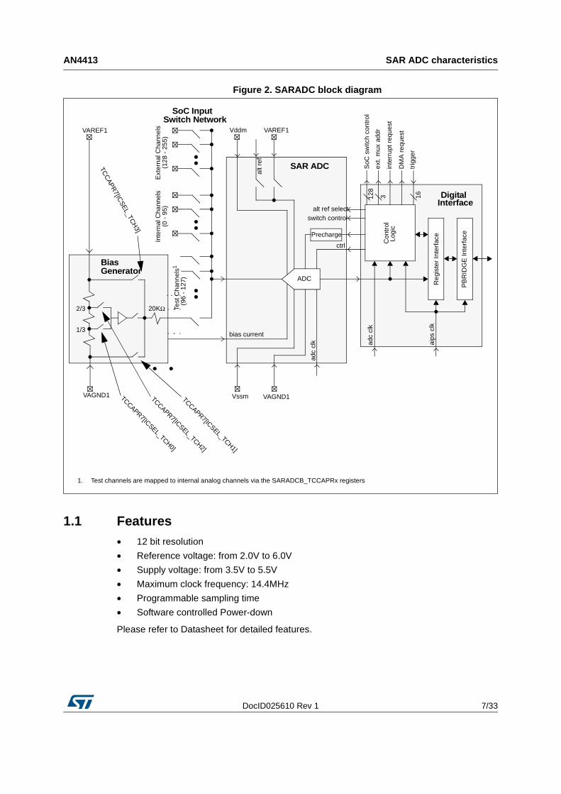
Figure 2. SARADC block diagram
1.1 Features• 12 bit resolution
• Reference voltage: from 2.0V to 6.0V
• Supply voltage: from 3.5V to 5.5V
• Maximum clock frequency: 14.4MHz
• Programmable sampling time
• Software controlled Power-down
Please refer to Datasheet for detailed features.
Precharge
20KΩ
ADC
2/3
1/3
Con
trol
Logi
c
adc
clk aips
clk
switch control
bias current
trig
ger
DM
A r
eque
st
ext.
mux
add
r
inte
rrup
t req
uest
SoC
sw
itch
cont
rol
Vddm
Vssm VAGND1
VAREF1
3 16128
Reg
iste
r In
terf
ace
Test
Cha
nnel
s1
(96
- 12
7)
Inte
rnal
Cha
nnel
s(0
- 9
5)SAR ADC
DigitalInterface
SoC InputSwitch Network
alt r
ef
adc
clk
ctrl
Bias
alt ref select
VAREF1
VAGND1
Ext
erna
l Cha
nnel
s(1
28 -
255
)
PB
RID
GE
Inte
rfac
e
1. Test channels are mapped to internal analog channels via the SARADCB_TCCAPRx registers
Generator
TCCAPR7[ICSEL_TCH0]
TCCAPR7[ICSEL_TCH2]
TCCAPR7[ICSEL_TCH1]
TCC
APR
7[ICSE
L_TCH
3]

SAR ADC characteristics AN4413
8/33 DocID025610 Rev 1
1.2 Considerations on the input impedance of the signal sourceTo preserve the accuracy of the ADC, it is necessary that analog input pins have low AC impedance. Placing a capacitor with good high frequency characteristics at the input pin of the device, can be effective: the capacitor should be as large as possible, ideally infinite.
This capacitor contributes to attenuating the noise present on the input pin; furthermore, its sources charge during the sampling phase, when the analog signal source is a high impedance source.
The impedance relative to the signal source can limit the ADC’s sample rate. Furthermore a current limiter resistance and an RC filter are often necessary to minimize the current request and to attenuate the noise present on the input pin. This external network can generate accuracy problems for the ADC converter and for this reason it is important to invest time in reaching the right adaptation.
Figure 3. SAR ADC input equivalent circuit

DocID025610 Rev 1 9/33
AN4413 SAR ADC characteristics
30
Figure 4. Input equivalent circuit (Fast SARn channels)
Figure 5. Input equivalent circuit (SARB channels)
The sampling capacitor Cs of the SAR, can be seen as a switching current sink element. The sampling capacitor switching at the conversion rate of the input channel can be seen as a resistive path to ground. For instance assuming a conversion rate of 400 ksps, with Cs equal to 6 pF a resistance of 417 kΩ (Req = 1/(fc.Cs)) is obtained.
To minimize the error induced by the voltage partitioning between this resistance (sampled voltage on CS) and the sum of RS + RF, the external circuit must be designed to respect the following relation.
RSW1
CP2 CS
VDD
Sampling
INTERNAL CIRCUIT SCHEME
RSW1 Channel Selection Switch ImpedanceRAD Sampling Switch ImpedanceCP Pin Capacitance (two contributions, CP1 and CP2)CS Sampling CapacitanceRCMSW Common mode switchRCML Common mode resistive ladder
CP1
RAD
ChannelSelection
Common modeswitch
Common moderesistive ladder
RSW1
CP3 CS
VDD
Sampling
RSW: Channel Selection Switch Impedance (two contributions RSW1 and RSW2)RAD: Sampling Switch ImpedanceCP: Pin Capacitance (three contributions, CP1, CP2 and CP3)CS: Sampling CapacitanceRCMSW: Common mode switchRCML: Common mode resistive ladder
CP1
RAD
ChannelSelection
CP2
Extended
RSW2
Switch
Common modeswitch
Common moderesistive ladder
INTERNAL CIRCUIT SCHEME
SAR ADC characteristics AN4413
10/33 DocID025610 Rev 1
which leads to follow this expression:
The formula above provides a constraint for the external network design, in particular on the resistive path.
The current limiting resistance value impacts the sampling time of the SAR. In order to run the SAR at the highest sampling speed, RL should respect the following constraint:
Of course, RL shall be sized also according to the current limitation constraints, in combination with RS (source impedance) and RF (filter resistance), due to some consideration on Nyquist theorem, and transfer charge, then a constraints on Cs is:
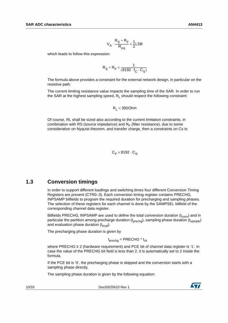
1.3 Conversion timingsIn order to support different loadings and switching times four different Conversion Timing Registers are present (CTR0–3). Each conversion timing register contains PRECHG, INPSAMP bitfields to program the required duration for precharging and sampling phases. The selection of these registers for each channel is done by the SAMPSEL bitfield of the corresponding channel data register.
Bitfields PRECHG, INPSAMP are used to define the total conversion duration (tconv) and in particular the partition among precharge duration (tprechg), sampling phase duration (tsample) and evaluation phase duration (teval).
The precharging phase duration is given by
tprechg = PRECHG * tck
where PRECHG ≥ 2 (hardware requirement) and PCE bit of channel data register is ‘1’. In case the value of the PRECHG bit field is less than 2, it is automatically set to 2 inside the formula.
If the PCE bit is ‘0’, the precharging phase is skipped and the conversion starts with a sampling phase directly.
The sampling phase duration is given by the following equation:
VA
RS RF+
Req----------------------⋅ 1
2---LSB<
RS RF+1
8192 fC CS⋅ ⋅( )----------------------------------------<
RL 350Ohm<
CF 8192 CS⋅>

DocID025610 Rev 1 11/33
AN4413 SAR ADC characteristics
30
tsample = INPSAMP * tck
where INPSAMP ≥ 4 (hardware requirement). In case the value of the INPSAMP bit field is less than 5, it is automatically set to 5 inside the SARADC.
The total evaluation phase duration is given by the following equations:
teval = 25 * tck
teval = 21 * tck (for 10-bit conversion)
The total conversion duration is (not including external multiplexing) given by the following:
tconv = tprechg + tsample + teval
The timings refer to the unit tck refers to reciprocal of fck, where fck = SARADC peripheral clock.
1.4 SARADC: constrain and timingThe integration of the ADC 10-bit module in the SARADC device leads to some further constraints to guarantee the performance indicated in the datasheet/electrical characteristics. In particular sampling time and conversion times must respect the minimum values, which are:
• 10 bit:
– Sampling time must be equal or greater than 555 ns
– Evaluation time must be equal or greater than 1454 ns
• 12 bit slow (SARADC_B):
– Precharge time must be equal or greater than 540 ns
– Sampling time must be equal or greater than 1500 ns
– Evaluation time must be equal or greater than 1712 ns
• 12 bit fast (SARADCx):
– Precharge time must be equal or greater than 270 ns
– Sampling time must be equal or greater than 750 ns
– Evaluation time must be equal or greater than 1712 ns
Table 1. 10 bit SARADC timing
Clock
(MHz)
TCK
(µs)PRECHG
INPSAMP
10 bit
(µs)
tPRECHG
(µs)
tSAMPLE
10 bit
(µs)
tEVAL
10 bit (µs)
tCONV
10 bit
(µs)
2 0.500 2 4 1.000 2.000 10.500 13.500
4 0.250 2 4 0.500 1.000 5.250 6.750
6 0.167 2 4 0.333 0.667 3.500 4.500
8 0.125 3 5 0.375 0.625 2.625 3.625
10 0.100 3 6 0.300 0.600 2.100 3.000
12 0.083 4 7 0.333 0.583 1.750 2.667

SAR ADC characteristics AN4413
12/33 DocID025610 Rev 1
14 0.071 4 8 0.286 0.571 1.500 2.357
14.6 0.068 4 9 0.274 0.616 1.438 2.329
Table 1. 10 bit SARADC timing (continued)
Clock
(MHz)
TCK
(µs)PRECHG
INPSAMP
10 bit
(µs)
tPRECHG
(µs)
tSAMPLE
10 bit
(µs)
tEVAL
10 bit (µs)
tCONV
10 bit
(µs)

DocID025610 Rev 1 13/33
AN4413 SD ADC characteristics
30
2 SD ADC characteristics
The Sigma-Delta Analog-to-Digital Converter (SDADC) digital interface block controls the on-chip SDADC feature. It provides an accurate conversion data and a conversion status for a wide range of applications.
In the figure below the block diagram of the SD ADC:
Figure 6. SDADC block architecture
Trig
ger
and
Gat
ing
Inte
rfac
eD
igita
l
conv
ersi
onre
sult
SD_CLK
interruptDMA32-bit R/W
PB
RID
GE
Clo
ckresu
lt fla
g
Int/D
MA
Gat
e
ΣΔA
nalo
g In
puts
BS
n-D
TB
Sn-
CK
VA
RE
F2
VA
GN
D2
mod
ulat
or c
trl
bias
ctr
l
filte
r ct
rl
mux
ctr
l
+ -
100K
Dig
ital
Filt
ers ΣΔ
AD
C
Bia
sA
VS
S
DIV
2
4:1 Differential8:1 Single-Ended
Mux
AV
DD
Gen
erat
or
DV
SS
DV
DD
AV
DD
/2
IRE
F
(ext
erna
l mod
ulat
or d
ata)
(ext
erna
l mod
ulat
or c
lock
)
Cas
cade
d 2-
2ΣΔ
Mod
ulat
or
Add
ition
alC
GM
Hig
h P
ass
Filt
er
SD
AD
C
Sig
nals
100K
100K
exte
rnal
trig
ger
wdg
cro
ssov
erev
ent (
mux
_adv
ance
)

SD ADC characteristics AN4413
14/33 DocID025610 Rev 1
2.1 Features• Conversion rate (Fs): up to 300 Ksps
• OSR = selectable from 24 to 256
• Passband = 0.33*Fs
• Programmable gain
• Differential/single ended operation
• Rail to rail (0 to 5 V) input common mode range
• High input impedance
• Very low current from references
• Provision for external modulator
• Selectable OSR/decimation rate
• Provision for gain/offset calibration
Please refer to datasheet for detailed features.
2.2 Considerations on the input impedance of the signal sourceTo preserve the accuracy of the ADC, it is necessary that analog input pins have low AC impedance. Placing a capacitor with good high frequency characteristics at the input pin of the device, can be effective: the capacitor should be as large as possible, ideally infinite.
This capacitor contributes to attenuate the noise present on the input pin; furthermore, its sources charge during the sampling phase, when the analog signal source is a high impedance source.
The impedance relative to the signal source can limit the ADC’s sample rate. Furthermore an RC filter is often necessary to minimize the current request and to attenuate the noise present on the input pin. This external network can generate accuracy problems for the ADC converter and for this reason it is important to invest time in reaching the right adaptation.
Figure 7. SDADC input equivalent circuit
DocID025610 Rev 1 15/33
AN4413 SD ADC characteristics
30
The recommend values are:
• Rest < 1 kΩ• Cf =1n to 10 nF
• Rf = max 1 kΩ
With this value the cutoff frequency is:
for
• Cf = 10 nF
• Rf = 1 kOhm
• fcutoff ≈ 15 kHz
2.3 SDADC and DMA When the first DMA request is being served (generated on FIFO Full condition) and on completion of this request then the SDADC will be disabled.
In order to prevent other FIFO FULL condition, it is necessary to disable the SDADC before disabling the DMA.
This means, it's necessary to disable the SDADC (and DMA transfer is enabled), in order:
– To stop the operation completely
– To change the channel configuration and re-initiate
In both these conditions, in order to have the operation safe it’s necessary to clear the DMA[EN] bit along with MCR[EN].
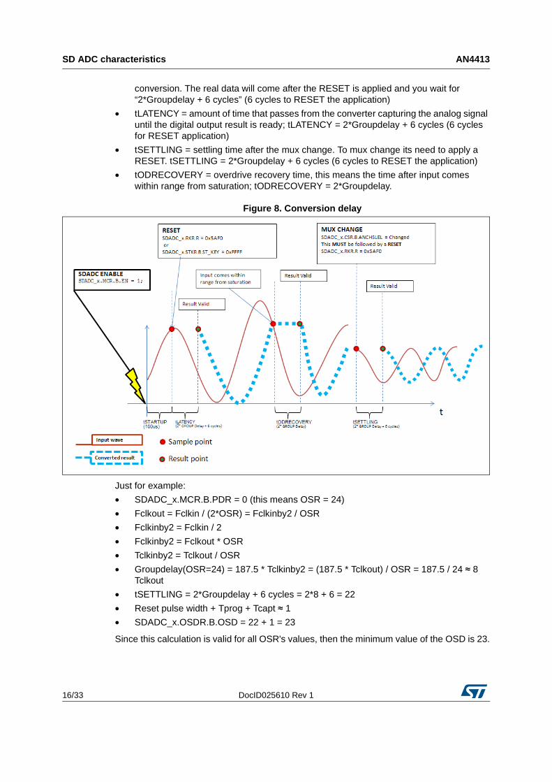
2.4 SDADC conversion timingThere are some registers and definitions to take in account for the SDADC conversion time:
• OSDR: the Output Settling Delay Register (OSD Field) provides a delay value to qualify the converted output data. The OSD field defines the delay to qualify the conversion data stored in the Converted Data Register (CDR). Whenever the SDADC block is reset in order to start the conversion from a fresh state, an internal timer is loaded with the OSD start value. The counter counts down with the output clock fd until it reaches ‘0’ and then it generates a flag which qualifies the converted data.
• fs is the input sampling clock frequency
• fd is the output clock
• δGROUP is the Groupdelay. The Groupdelay depend on OSR value
• tSTARTUP is the start-up time from the power down state. The ADC is “ready” EN is pulled to ‘1’. After tSTARTUP time it’s possible to apply a RESET and start a
fcutoff1
2π Rf Cf⋅ ⋅---------------------------=
fdfS
2 OSR×-----------------------=
SD ADC characteristics AN4413
16/33 DocID025610 Rev 1
conversion. The real data will come after the RESET is applied and you wait for “2*Groupdelay + 6 cycles” (6 cycles to RESET the application)
• tLATENCY = amount of time that passes from the converter capturing the analog signal until the digital output result is ready; tLATENCY = 2*Groupdelay + 6 cycles (6 cycles for RESET application)
• tSETTLING = settling time after the mux change. To mux change its need to apply a RESET. tSETTLING = 2*Groupdelay + 6 cycles (6 cycles to RESET the application)
• tODRECOVERY = overdrive recovery time, this means the time after input comes within range from saturation; tODRECOVERY = 2*Groupdelay.
Figure 8. Conversion delay
Just for example:
• SDADC_x.MCR.B.PDR = 0 (this means OSR = 24)
• Fclkout = Fclkin / (2*OSR) = Fclkinby2 / OSR
• Fclkinby2 = Fclkin / 2
• Fclkinby2 = Fclkout * OSR
• Tclkinby2 = Tclkout / OSR
• Groupdelay(OSR=24) = 187.5 * Tclkinby2 = (187.5 * Tclkout) / OSR = 187.5 / 24 ≈ 8 Tclkout
• tSETTLING = 2*Groupdelay + 6 cycles = 2*8 + 6 = 22
• Reset pulse width + Tprog + Tcapt ≈ 1
• SDADC_x.OSDR.B.OSD = 22 + 1 = 23
Since this calculation is valid for all OSR's values, then the minimum value of the OSD is 23.

DocID025610 Rev 1 17/33
AN4413 SD ADC characteristics
30
2.5 Data conversion stepTo acquire a data from the SDADC, the following sequence is required:
1. Enable the SDADC by asserting MCR[EN]
2. Configure MCR to select the required mode, polarity, common mode voltage, input gain, and decimation rate
3. Enable high-pass filter is required
4. Select the required analog channel for data conversion. It is possible to select the bias for each channel for AC coupling applications.
5. Configure the OSD delay according to the SDADC required startup time or latency from the reset exit
6. Generate a reset event writing 0x5AF0 in RESET_KEY field of the RKR register
7. Wait till FIFO empty flag DFEF of SFR register is clear
8. Read data by CDATA of CDR register
If you need to change of channel then:
1. Select the required analog channel for the data conversion. It is possible to select the bias for each channel for AC coupling applications
2. Generate a reset event writing 0x5AF0 in RESET_KEY field of the RKR register
3. Wait till FIFO empty flag DFEF of SFR register is clear
4. Read data by CDATA of CDR register
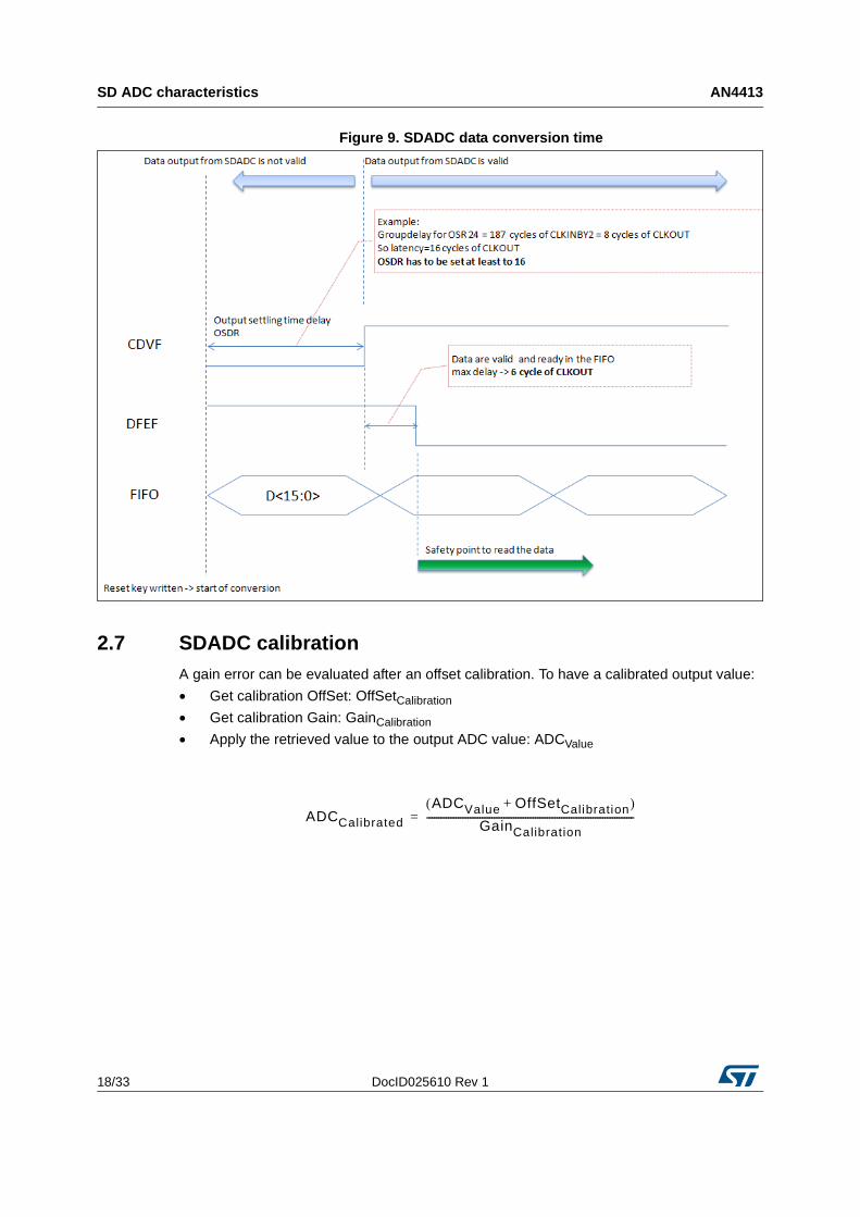
2.6 Data conversion timingThe time elapsed between a reset event and a Read data by the CDATA field of the CDR register are:
• Reset event ÷ Data Valid flag(CDVS) = output settling time delay (OSDR has to be set at least to 16)
• Data Valid flag ÷ Data FIFO is not empty = 0.5*CLK_Out + 3*CLK_In
• Data FIFO is not empty ÷ read Data (safety point) = 2*CLK_In
where:
CLK_Out = CLK_In/(2*OSR)
SD ADC characteristics AN4413
18/33 DocID025610 Rev 1
Figure 9. SDADC data conversion time
2.7 SDADC calibration A gain error can be evaluated after an offset calibration. To have a calibrated output value:
• Get calibration OffSet: OffSetCalibration
• Get calibration Gain: GainCalibration
• Apply the retrieved value to the output ADC value: ADCValue
ADCCalibrated
ADCValue OffSetCalibration+( )GainCalibration
--------------------------------------------------------------------------------------=

DocID025610 Rev 1 19/33
AN4413 SD ADC characteristics
30
Figure 10. SDADC calibration
2.8 Offset calibration procedureTo perform offset calibration, the following sequence must be applied:
1. Select differential mode of operation by writing MCR[MODE] to ‘0’
2. Configure the mux selection ANCHSEL field of CSR to ‘100’ or ‘101’ as required
a) CSR = ‘100’ in case of data conversion after calibration in “single ended mode with negative input = VSS_HV_ADR_D”
b) CSR = ‘101’ in case of data conversion after calibration in “differential mode” and “single ended mode with negative input = (VDD_HV_ADR_D - VSS_HV_ADR_D)/2”
3. Disable the bias on all the input analog channels by writing ENBIAS field of CSR to 0x00.
4. Disable the high pass filter by deasserting MCR[HPFEN]
5. Generate a reset event by writing 0x5AF0 to RESET_KEY of RKR
6. Read the digital output stored in FIFO after the output settling time
7. The measured offset can be used to nullify the offset error in the digital output. Expected output is 0b00_0000_0000_0000. The SDADC offset can be calculated as:
Offset = Expected Output – Actual Output
The offset must be calculated for each PGAN field setting since it is expected to vary with the gain configuration of SDADC.
2 1 3
1. Original ADC response
2. Offset corrected after Add
operation
3. Slope corrected after multiply
operation
Input Voltage
Out
put C
ode
SD ADC characteristics AN4413
20/33 DocID025610 Rev 1
2.9 Gain calibration stepTo perform a gain calibration, the following sequence needs to be applied:
1. Select the differential mode of operation by writing MCR[MODE] to ‘0’.
2. Enable the Accurate Gain Error Mode Enable by writing MCR[GECEN] to ‘1’.
3. Configure the mux selection ANCHSEL field of CSR to ‘110’. This configuration will apply VREFP on positive terminal and VREFN on negative terminal.
4. Disable the bias on all the input analog channels by writing ENBIAS field of CSR to 0x00.
5. Disable the high-pass filter by deasserting MCR[HPFEN].
6. Generate a reset event by writing 0x5AF0 to the RESET_KEY field of RKR register.
7. Read the digital output (Dp) stored in FIFO after the output settling time. Expected output if there is no gain error is 0b0111_1001_1001_1001, corresponding to full positive scale after attenuation inserted by the internal filter (1*0.95). The measurement should be repeated to reduce contribution of noise during calibration process. Dp is the average value of attenuated positive full scale given by Dp = AVERAGE(CDR[CDATA])
8. Change the mux selection ANCHSEL field of CSR to ‘111’. This configuration will apply VREFN on positive terminal and VREFP on negative terminal.
9. Generate a reset event by writing 0x5AF0 to RESET_KEY of RKR.
10. Read the digital output (Dn) stored in the FIFO after the output settling time. Expected output if there is no gain error is 0b1000_0110_0110_0110, corresponding to the full negative scale after attenuation inserted by the internal filter (-1*0.95). The measurement should be repeated to reduce contribution of noise during the calibration process. Dn is the average value of an attenuated negative full scale given by Dn = AVERAGE(CDR[CDATA])
11. The SDADC error can be calculated as: Gain = (Dp – Dn) / 216
12. The measured gain value can be used to nullify the gain errors in the digital output.
During the calibration, the number of full scale conversion (Dp, Dn) is directly correlated to the rejection of noise.
The value conversion is depending on the application noise. It is recommended to run at least 16 conversions before calculating the average value.
For a calibrated conversion, the data CDR[CDATA] provided by the SDADC should be normalized using the calculated gain:
CDATAnorm = CDR[CDATA]/Gain

DocID025610 Rev 1 21/33
AN4413 SAR vs SD
30
3 SAR vs SD
In Table 2 a short comparison between the two kinds of ADC.
Table 2. SAR ADC vs SD ADC
SAR ADC SD ADC
+ Fast signal acquisition + High dynamic signals
+ Fast input signal multiplexing + Strongly monotonic by design
+ DC signals + Fast AC signals
- Resolution is limited + High resolution possible with less effort
- Demanding in terms of technology (matching of components parameters)
- Input signal switching takes time

ADC: automotive use cases AN4413
22/33 DocID025610 Rev 1
4 ADC: automotive use cases
In Table 3 a short comparing between the two kinds of ADC, automotive use cases.
Table 3. ADC automotive use cases
SAR ADC SD ADC
Signal acquisition– Temperature: water, oil, air– Pressure: fuel, oil, air– Position: flaps for air inlet and outlet, actuators,
sensors– Human interfaces: switches, pedals, levers
– Movement: acceleration, deceleration
Combustion parameters– Knock detection– Exhaust gas analysis
Diagnosis– Sensors and actors– Supply monitoring
Battery management– Cell balancing inside smart lithium ion batteries
Audio & Video signals– Entertainment– Voice to command

DocID025610 Rev 1 23/33
AN4413
30
Appendix A
It is supposed that the peripherals had got a reset default configuration. For a full specification refer to the SPC574Kxx reference manual and datasheet (see Section B.1: Reference documents).
Whenever a register or a register bit field is referred, the following notation applies:
PERIPHERAL_NAME.REG_NAME[index].R //register access
PERIPHERAL_NAME.REG_NAME[index].B.BIT_NAMEx //bit field
where,
• index is used if more than one register with the same functionality exist within a peripheral (for example a timer with 16 channels, then it would have 16 control registers for each channel one);
• x is used when more than one bit with the same functionality exists within a register (e.g. 5 chip select enable bits). Peripheral name may be omitted when the context is obvious.
For example: SDACD_0.MCR.B.EN, refers to the EN bit from MCR register in ADADC_0 peripheral.
AN4413
24/33 DocID025610 Rev 1
A.1 Offset calibration procedure
Figure 11. Offset calibration procedure
DocID025610 Rev 1 25/33
AN4413
30
4.1 Gain calibration procedure
Figure 12. Gain calibration procedure

AN4413
26/33 DocID025610 Rev 1
4.2 SDADC_0 CH2 setting
Figure 13. SDADC_0 CH2 setting
4.3 Test N.1: SDADC0_ CH2 acquisition The follow example shows the SDADC0_CH0 acquisition with and without calibration.
The code in MAIN program is:

DocID025610 Rev 1 27/33
AN4413
30
Figure 14. Test N.1: SDADC0_ CH2 Acquisition
4.3.1 CH2 acquisition values: 5V
By the board potentiometer, the input voltage on CH2 has been set to 5 V.
With this setting, the results are:

AN4413
28/33 DocID025610 Rev 1
Figure 15. CH2 acquisition values: 5V
4.3.2 CH2 acquisition values: 0 - 5V
By the board potentiometer, the input voltage on CH2 has been set from 0 V to 5 V.
With this setting, the results are:
DocID025610 Rev 1 29/33
AN4413
30
Figure 16. CH2 acquisition values: 0 - 5V
4.4 Test N.2: SDADC0_ CH2 acquisition with biasThe following example shows the SDADC0_CH0 acquisition with bias on negative input. This means that the:
negative input = (VDD_HV_ADR_D - VSS_HV_ADR_D)/2.
4.4.1 SDADC_BIAS_Set
To set the bias on negative terminal, to enable the VCOMSEL, and respective BIASEN field:
Figure 17. SDADC_BIAS_Set

AN4413
30/33 DocID025610 Rev 1
4.4.2 CH2 acquisition values: -2.5 V - +2.5 V
The acquisition results, show the -2.5 V for an input pin value at 0 V, and +2.5 V for input pin value at 5 V.
The acquired values are not by regular steps, because the increase of the input value is obtained via a potentiometer rotated by hand.
Figure 18. CH2 acquisition values: -2.5 V - +2.5 V
DocID025610 Rev 1 31/33
AN4413 Other information
32
Appendix B Other information
B.1 Reference documents• SPC574Kxx - 32-bit Power Architecture® based MCU for automotive applications
(RM0334, Doc ID 023671)
• 32-bit Power Architecture® based MCU for automotive applications (SPC574K72E5, SPC574K72E7 Datasheet, Doc ID 023601)
B.2 Acronyms
Table 4. Acronyms
Acronym Name
SDADC Sigma-Delta Analog-to-Digital Converter
SARADC Successive Approximation Analog-to-Digital Converter
Revision history AN4413
32/33 DocID025610 Rev 1
Revision history
Table 5. Document revision history
Date Revision Changes
02-Dec-2013 1 Initial release.

DocID025610 Rev 1 33/33
AN4413
33
Please Read Carefully:
Information in this document is provided solely in connection with ST products. STMicroelectronics NV and its subsidiaries (“ST”) reserve the right to make changes, corrections, modifications or improvements, to this document, and the products and services described herein at any time, without notice.
All ST products are sold pursuant to ST’s terms and conditions of sale.
Purchasers are solely responsible for the choice, selection and use of the ST products and services described herein, and ST assumes no liability whatsoever relating to the choice, selection or use of the ST products and services described herein.
No license, express or implied, by estoppel or otherwise, to any intellectual property rights is granted under this document. If any part of this document refers to any third party products or services it shall not be deemed a license grant by ST for the use of such third party products or services, or any intellectual property contained therein or considered as a warranty covering the use in any manner whatsoever of such third party products or services or any intellectual property contained therein.
UNLESS OTHERWISE SET FORTH IN ST’S TERMS AND CONDITIONS OF SALE ST DISCLAIMS ANY EXPRESS OR IMPLIED WARRANTY WITH RESPECT TO THE USE AND/OR SALE OF ST PRODUCTS INCLUDING WITHOUT LIMITATION IMPLIED WARRANTIES OF MERCHANTABILITY, FITNESS FOR A PARTICULAR PURPOSE (AND THEIR EQUIVALENTS UNDER THE LAWS OF ANY JURISDICTION), OR INFRINGEMENT OF ANY PATENT, COPYRIGHT OR OTHER INTELLECTUAL PROPERTY RIGHT.
ST PRODUCTS ARE NOT DESIGNED OR AUTHORIZED FOR USE IN: (A) SAFETY CRITICAL APPLICATIONS SUCH AS LIFE SUPPORTING, ACTIVE IMPLANTED DEVICES OR SYSTEMS WITH PRODUCT FUNCTIONAL SAFETY REQUIREMENTS; (B) AERONAUTIC APPLICATIONS; (C) AUTOMOTIVE APPLICATIONS OR ENVIRONMENTS, AND/OR (D) AEROSPACE APPLICATIONS OR ENVIRONMENTS. WHERE ST PRODUCTS ARE NOT DESIGNED FOR SUCH USE, THE PURCHASER SHALL USE PRODUCTS AT PURCHASER’S SOLE RISK, EVEN IF ST HAS BEEN INFORMED IN WRITING OF SUCH USAGE, UNLESS A PRODUCT IS EXPRESSLY DESIGNATED BY ST AS BEING INTENDED FOR “AUTOMOTIVE, AUTOMOTIVE SAFETY OR MEDICAL” INDUSTRY DOMAINS ACCORDING TO ST PRODUCT DESIGN SPECIFICATIONS. PRODUCTS FORMALLY ESCC, QML OR JAN QUALIFIED ARE DEEMED SUITABLE FOR USE IN AEROSPACE BY THE CORRESPONDING GOVERNMENTAL AGENCY.
Resale of ST products with provisions different from the statements and/or technical features set forth in this document shall immediately void any warranty granted by ST for the ST product or service described herein and shall not create or extend in any manner whatsoever, any liability of ST.
ST and the ST logo are trademarks or registered trademarks of ST in various countries.Information in this document supersedes and replaces all information previously supplied.
The ST logo is a registered trademark of STMicroelectronics. All other names are the property of their respective owners.
© 2013 STMicroelectronics - All rights reserved
STMicroelectronics group of companies
Australia - Belgium - Brazil - Canada - China - Czech Republic - Finland - France - Germany - Hong Kong - India - Israel - Italy - Japan - Malaysia - Malta - Morocco - Philippines - Singapore - Spain - Sweden - Switzerland - United Kingdom - United States of America
www.st.com