special-purpose devices for signal and image processing ...htk/publication/1980-spie-kung.pdf ·...
TRANSCRIPT

Carnegie Mellon UniversityResearch Showcase @ CMU
Computer Science Department School of Computer Science
1980
Special-purpose devices for signal and imageprocessing : an opportunity in VLSIH. T. KungCarnegie Mellon University
Follow this and additional works at: http://repository.cmu.edu/compsci
This Technical Report is brought to you for free and open access by the School of Computer Science at Research Showcase @ CMU. It has beenaccepted for inclusion in Computer Science Department by an authorized administrator of Research Showcase @ CMU. For more information, pleasecontact [email protected].
Recommended Citation, , , -
NOTICE WARNING CONCERNING COPYRIGHT RESTRICTIONS: The copyright law of the United States (title 17, U.S. Code) governs the making of photocopies or other reproductions of copyrighted material. Any copying of this document without permission of its author may be prohibited by law.

C M U - C S - 8 0 - 1 3 2
Special-Purpose Devices for Signal and Image Processing: An Opportunity in VLSI
H. T. Rung
Department of Computer Science Carnegie-Mellon University
Pittsburgh, Pennsylvania 15213
July 1980
This paper is to be presented at SPIE's 24th Annual Technical Symposium, San Diego, California, July 28-August 1, 1980. The research was supported in part by the Office of Naval Research under Contracts N00014-76-C-0370 and N00014-80-C-0236, in part by the National Science Foundation under Grant MCS 78-236-76, and in part by the Defense Advanced Research Projects Agency under Contract F33615-78-C-1551 (monitored by the Air Force Office of Scientific Research).
UNIVERSITY LIBRARIES CARNEGIE-MELLON UNIVERSITY
PITTSBURGH. PENNSYLVANIA 15213

Special-purpose devices for signal and image processing: an opportunity in VLSI
H. T. Rung
Department of Computer Science, Carnegie-Mellon University, Pittsburgh, Pennsylvania 15213
Abstract
Based on the systolic array approach, new designs of special-purpose devices for filtering, correlation, convolution, and discrete Fourier transform are proposed and discussed. It is argued that because of high degrees of simplicity, regularity and concurrency inherent to these designs, their VLSI implementation will be cost effective.
Introduction
LSI technology allows tens of thousands of devices to fit on a single chip; VLSI technology promises an increase of this number by at least one order of magnitude in the next decade. Both the opportunities and challenges presented by VLSI are tremondous. This paper proposes and discusses the use of die systolic array approach in the construction of special-purpose VLSI devices for signal and image processing. These devices are to be attached to a host, which can be a conventional computer or another special-purpose system.
Systolic arrays is an architecture first proposed for implementation of matrix operations in VLSI. 1 Typically a systolic array enjoys the following properties:
1. The array can be implemented with only a few types of simple cells.
2. The data and control flow of the array is simple and regular, so that cells can be connected by a network with local and regular interconnections; long distance or irregular communication is not needed.
3. The array uses extensive pipelining and multiprocessing. Typically, several data streams move at constant velocities over fixed paths in the network, and interact where they meet. In this fashion, a large proportion of the processors in the array are kept active, so that the array can sustain a high rate of computation flow.
4. The array makes multiple uses of each input data item. As a result, high computation throughput can be achieved without requiring high bandwidth between the array and the host.
VLSI designs based on systolic arrays tend to be simple (a consequence of properties 1 and 2), modular (property 2), and of high performance (properties 3 and 4). Therefore systolic arrays are suitable for VLSI implementation. Examples and further discussions of the attractiveness of systolic arrays can be found in other papers . 2 , 3 ' 4 , 5 In this paper we illustrate the use of systolic arrays in performing several important operations in signal and image processing.
Systolic arrays for filtering
This section discribes the basic design of a family of systolic arrays for performing filtering. Designs of systolic arrays for convolution, correlation and pattern matching can be obtained similarly6, so they will not be discussed separately here. Mathematically the canonical form of the filtering problem can be defined as follows:
given the weighting cofficients {wQ, w^ w h } , {r^ r 2 r k ] , the initial values fr-k> y-k + i' y - l* ' a n d ^ i n P u t s c Q u c n c e fr-fr x_h + 1 , xQ, x p x j ,

2
compute the output sequence {y 0 , y^ y n } defined by Vi = 2 h
j = 0 wj xi-j + 2 k j = l fjyi-j-Assume that a cycle is the time to perform the function of the type I cell defined below (which in this case
is essentially the time for two multiplications and two additions). Systolic arrays proposed here can compute a new y{ every two cycles. (Systolic arrays for Finite Impulse Response (FIR) and Infinite Impulse Response (HR) filters were previously considered separately by the author. 2)
The weighting coefficients w^s and r^s are preloaded to a systolic array. The filtering computation starts by loading the x^s from the host to the systolic array in the natural ordering, that is, x. h first, x _ h + 1 second, x . h + 2
third, and so on. Immediately after the systolic array has received all the x^s for -h < i < 0, it starts outputting the computed y^s in the natural ordering at the rate of one every two cycles.
Description of the systolic filtering array
Basic cells. There are two types of cells, as depicted in Figure 1. A type II cell is essentially a buffer.
TYPE I CELL
Y i n ^ r r i i 1
L w
You!
Yout r r i i 1
L w
Y r r i i 1
L w ^—-— * o u L
r r i i 1
L w
Yout «- y i n
Yout <• w - x i n + r . y i n + Y j n
ut
TYPE II CELL:
[VALUES r AND w ARE PRELOADED WEIGHTING COEFFICIENTS]
Yout
Yout <- Yj,
fout Y
Figure 1
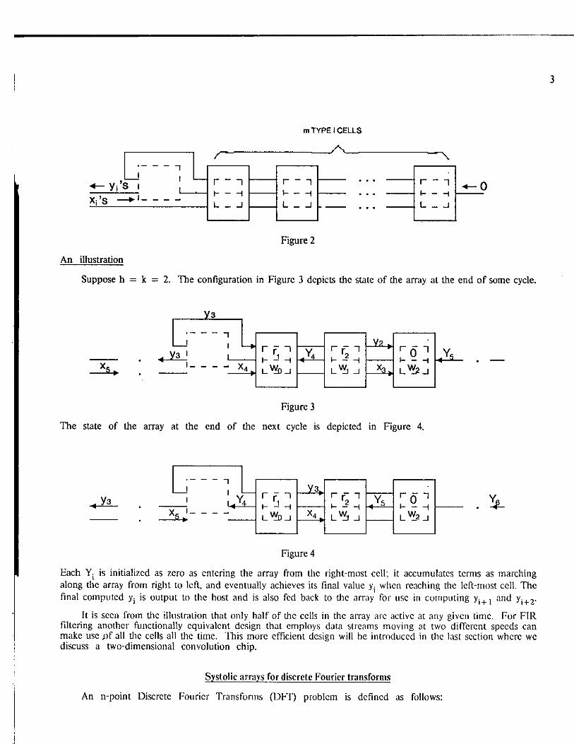
The array. Let m = max(h + l, k). The systolic array is a linear array consisting of m type 1 cells and one type 11 cell, as depicted in Figure 2. The right-most cell is a degenerated type I cell, where input Y. is always zero, and outputs y Q U t and x Q u t are ignored.
3
Yi'S i
r
I 1 I 1 I I
m TYPE I CELLS
I 1 I 1 I I
I 1 I 1 I I
Figure 2
An illustration
Suppose h = k = 2. The configuration in Figure 3 depicts the state of the array at the end of some cycle.
Y3
1 1
1 1
1 ' i 1
\r - H
r r i 1- 2 H
Y2 „ 1 ' i 1
\r - H
r r i 1- 2 H . x 4 >
1 ' i 1
\r - H
r r i 1- 2 H
1 ' i 1
\r - H
r r i 1- 2 H
Figure 3
The state of the array at the end of the next cycle is depicted in Figure 4.
Y3
. 1 1 . 1 1
1 r1 ' 1- — H
r r i • « Y *
1 r1 ' 1- — H
r r i
x 5 ;
1 r1 ' 1- — H
r r i
w
1 r1 ' 1- — H
r r i
Figure 4
Each Y t is initialized as zero as entering the array from the right-most cell; it accumulates terms as marching along the array from right to left, and eventually achieves its final value y. when reaching the left-most cell. The final computed y{ is output to the host and is also fed back to the array for use in computing y i + 1 and y i + 2 -
It is seen from the illustration that only half of the cells in the array are active at any given time. For FIR filtering another functionally equivalent design that employs data streams moving at two different speeds can make use jof all the cells all the time. This more efficient design will be introduced in the last section where we discuss a two-dimensional convolution chip.
Systolic arrays for discrete Fourier transforms
An n-point Discrete Fourier Transforms (DFT) problem is defined as follows:

given {a 0 , ax, a ^ } , compute {y 0, yv ynml} defined by
J i j = 0 j ' where co is an n-th root of unity.
The well-known Fast Fourier Transform (FFT) algorithm computes an n-point DFT in 0(n log n) operations, while the straightforward method requires 0(n 2) operations. However, for parallel processing, the FFT suffers from the drawback that it requires complicated data communication (see discussions below). Here we describe a family of systolic arrays for computing DFTs in parallel that use only the simplest communication scheme, namely, the linearly connected array.
Description of the systolic DFT array
Basic cell. Figure 5 describes the basic cell:
x in X out < - X i n
Y i n , i a , Yo'ut^ Yout < - Y i n - x i n + a W — —
[VALUE a IS A PRELOADED INPUT]
Figure 5
The array. A full array consists of n-1 linearly connected basic cells, as depicted in Figure 6.
< o " S - * r ~~ i r ~" i a n . - . - * 1^-2 1 ^n-1 »
I I
i a o ' y . ' s " I I
i a o ' y . ' s " I I
i a o '
Figure 6
The input Y i n and x i n to the left-most cell is a n - 1 and some power of co, respectively, whereas the output x Q U t
from the right-most cell is always ignored.
An illustration
Consider the case n = 5. A 5-point DFT problem can be viewed as that of evaluating the polynomial
a 4 x 4 + a 3 x 3 + a 2 x 2 -f a xx + a 0
at x = 1, co, co2, co 3, co4, where co is a fifth root of unity. Evaluating the polynomial by Horner's rule gives:
>'o = (((a 4-l + a 3)-l + a 2)-l + a^-1 + aQ,
*1 = (((a4-w + a3)-w + a2)-<o + a^-w + a 0,
(((a 4
-(o 2 + a3)-<o2 + a 2 ) - w 2 + a^-w 2 + aQ,
ys = (((a 4 'w 3 + a3)*w3 + a2)"co3 + a^-w 3 + a0>
y 4 = (((a 4
-oj 4 + a 3 ) - w 4 + a 2)'co 4 + a^-w 4 + a 0.
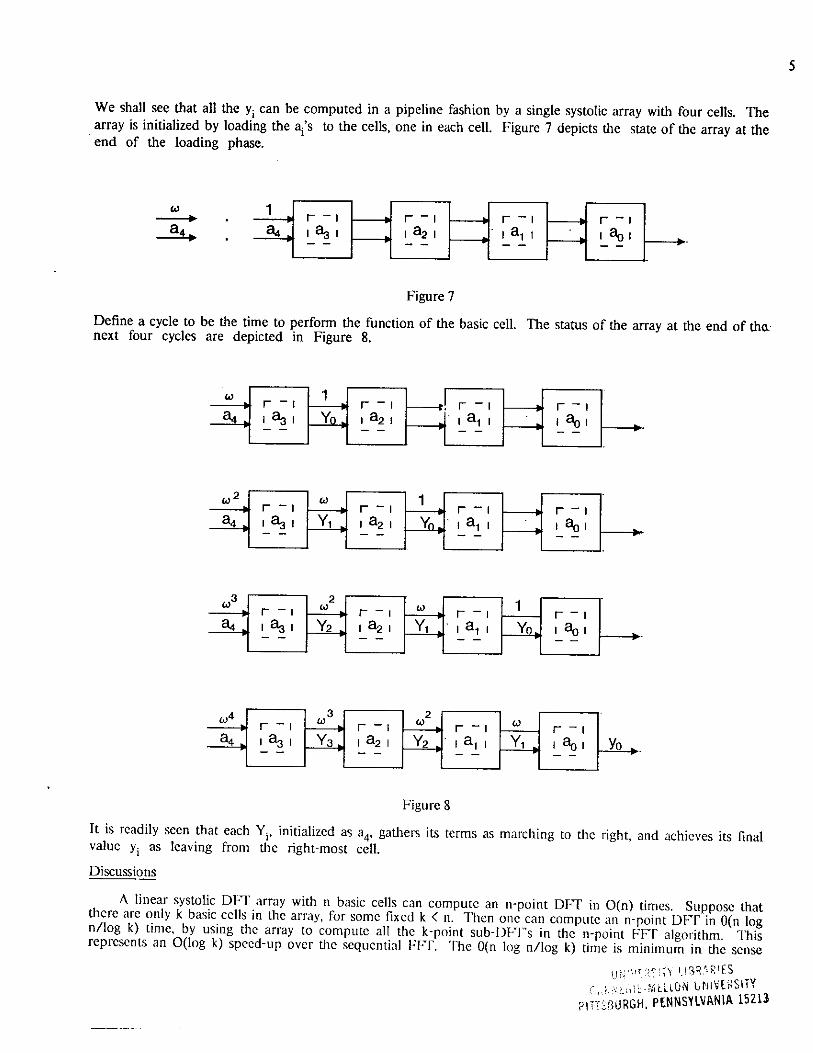
We shall see that all the y{ can be computed in a pipeline fashion by a single systolic array with four cells. The array is initialized by loading the a t's to the cells, one in each cell. Figure 7 depicts the state of the array at the end of the loading phase.
1 - ^ r ~ i p ~~ i p ~ I 1— — 1
*** i &3 i w i 8 2 i ' l a 1 I • 1 1 I ^o l w p
Figure 7
Define a cycle to be the time to perform the function of the basic cell. The status of the array at the end of tha next four cycles are depicted in Figure 8.
CO » 1 — 1
1 8 3 1
1 I I I a 2 I
• 1- — 1 I I
I 8o I
CO » 1 — 1
1 8 3 1 Y q „
I I I a 2 I " 1 a i I
^ I I
I 8o I
1 — 1
1 8 3 1
I I I a 2 I " 1 a i I
I I
I 8o I • -
0> 2
^ r ~~ i
CO r ~ i
1 f— — I I — I I 8q i i 8 3 i I a 2 I • I a 1 I ^ I — I I 8q i
• CO
^ • r ~ i 2
CO r — I CO r~ — 1 1 1— — 1
**> i 83 i I 8 2 i ^
Y1 „ 1 1 1 a i i Y 0 f c
1 1 l 8q 1
^
^ P ~" 1 3
CO r ~~ 1
2 CO r~ — 1 CO f— — I
1 8 3 | 1 8 2 1 1 1
' 1 a i 1 Y1 „
1 1 l 8q 1 "' w ! p —^_•
Figure 8
It is readily seen that each initialized as a 4, gathers its terms as marching to the right, and achieves its final value y i as leaving from the right-most cell.
Discussions
A linear systolic DFT array with n basic cells can compute an n-point DFT in O(n) times. Suppose that diere are only k basic cells in the array, for some fixed k < n. Then one can compute an n-point DFT in 0(n log n/log k) time, by using the array to compute all the k-point sub-DPTs in the n-point FFT algorithm. This represents an 0(log k) speed-up over the sequential FFf. The 0(n log n/log k) time is minimum in the sense
y f ^/ r ocav U3RAKIES
r ^ i i E - t t £ L l O N UNIVERSITY PITTSBURGH, PENNSYLVANIA 15213

6
that when executing an n-point FFT on a device with O(k) words of local memory (as in the case of the systolic array where k words of memory are distributed among k cells), this amount of time is needed just to transfer data between the host and the device.
Up to this point we have been assuming implicidy that the rate that data is sent to the systolic array is not higher than the computation rate of a basic cell. If this is not the case, then to take advantage of the available bandwidth, as many independent linear systolic DFT arrays should be used as possible, so that all the arrays can input and output data in each cycle. An interesting (but maybe theoretical) comparison to the parallel FFT can be made at this point. The traditional parallel implementation of the FFT algorithm assumes that k words of inputs and outputs are performed every log k cycles, using a shuffle-exchange network of k nodes. 7 , 8 The parallel FFT using such a network performs an n-point DFT in 0((n log n)/k) time and the best known layout of the network takes a chip area 0(k 2 / log k). 9 A set of k/log k linear systolic DFT arrays, each consisting of k basic cells, achieves the same performance with the same total chip area, but enjoys a much simpler, communication structure.
The systolic approach has one more advantage in that with minor control mechanisms the same systolic array may be used for many computations such as filtering, DFT and matrix multiplication.
Remarks on Implmentation and Performance-
For simplicity, we have so far assumed that cells in systolic arrays operate on words. In unplementationi. each word processor can be partitioned into bit processors to achieve modularity at the bit-level. A transformation of a design from word-level to bit-level is usually straightforward.3 It is also possible to implement cells efficiently with multi-stage pipeline adders and multipliers. In general, many variations on the systolic arrays suggested are possible. All of these are functionally equivalent, and differ only in implementation details.6
Using the bit-serial implementation, it is possible to implement about ten basic cells, performing 32-bit fixed-point operations, on a single chip with present MOS technology. By using many such chips, the systolic, array can achieve a high computation rate even assuming a rather limited bandwidth between the array and the host. This is because each word once input from the host is used many times in the array..
A Two-Dimensional Convolution Chip)
During the past year, we have designed prototypes of several special-purpose chips at CMU using the systolic approach. These include a pattern-match chip, 3 an image-processing chip, and a tree processor for database applications. 1 1 The pattern-match and tree processor chips have been tested and found to work. The image processing chip will be tested after the required testing software is developed. Here we sketch the function and overall design of this image processing chip; for details of the design the reader is referred to the project.
report. 1 0
Yir I 1
Xout^ Y o u t <- W • X i n + Yin
Yout^ X <- x i n
Xout «- X
[EACH x STAYS INSIDE THE CELL FOR ONE CYCLE]
[VALUE w IS A PRELOADED WEIGHTING COEFFICIENT]
Figure 9
The chip performs the two-dimensional convolution operator and is based on a variant of the systohc FIR filtering array described earlier. The chip uses essentially only one type of basic cells (see Figure 9), which aie

interconnected in a completely regular and modular way to form a two-dimensional systolic array.
To define the convolution problem, consider a matrix X = {x ; j } and a kxk window with weighting coefficients w y as shown in Figure 10. For the purpose of illustration, we use k = 3. Now slide the 3x3 window along the matrix. For each position of the window, the weighted sum of the terms in the submatrix covered bv the window is to be computed.
X =
X 1 1 X 1 2 X 1 3 X 1 4 X 2 1 X 2 2 X 2 3 * 2 4 X 3 1 X 3 2 X 3 3 X 3 4
X n 1 X n 2 X n 3 ^ 4
w 11
W v12
W 1 3
w w 2 1
W W 2 2
W 2 3
w w 3 1
W v 3 2
W 3 3
W = WEIGHTING
COEFFICIENTS
3x3 WINDOW
Figure 10
In Figure 11 five rows of the matrix X advance synchronously from left to right. The small dots in the figure denote appropriate delays such that a same column advances as a whole. (This does not mean that such delays have to be implemented on-chip; the inputs can be spaced accordingly when fed into the device.) Three kernel cells are shown in the figure, each one being composed of nine basic cells and one row-interface cell whose function will become clear later. Whenever an element x- emerges from the upper right basic cell of a kernel cell, the weighted sum corresponding to a submatrix with that element as the upper right element is being output from that kernel cell. Therefore by sweeping the first five rows a systolic array consisting of three kernel cells can compute the first three rows on-the-fly. In general, by sweeping rows 3i-fl to 3i + 5 the array computes rows 3i-fl to 3i + 3. Thus a pixel in the image is input to the array at most twice.
X 1 3 X I 2 X 1 1
^23 \ l *21
•" X 4 3 ^ 2 X 4 1
'•" ^ 3 ^ 2 ^ 1
KERNEL CELL A i RESULT
KERNEL CELL i RESULT
RESULT
KERNEL CELL f
Figure 11
Now consider Figure 12 (a) where three basic cells in the first row of a kernel cell is shown Consider the moment an element x y enters the left-most basic cell. Denote by Y the particular Y m to
initialized as zero. During the cycle X i j enters the left-most cell, Y becomes w 1 3 -x y . In the next cycle w 1 2-x.. is
accumulated to Y, as shown in Figure 12 (b). Finally, as in Figure 12 (c), y,^ is further accumulated to Y

8 As a result, when Y emerges at the last cell, it has already accumulated the weighted sum of the first row of a submatrix. In the meanwhile, the same has been happening at the two bottom rows of the kernel cell. Therefore, by summing the partial results at the row-interface cell, the desired output is obtained.
Note that each row of the kernel is simply a linear systolic FIR filtering array. This filtering array differs from that discussed earlier (in Figures 1 to 4 with ^ = 0) in that both the x-stream and Y-stream now move from left to right and the x-stream travels twice as slow as the Y-stream. This variation results in the active use of every cell at any given time.
(a) —M r ~ I h
x L M H
L_W13_J LW12_J 5̂H
(b) r x " "i
LW12_. | W l J _ J
(c) ij.+ L,
LW13_J X;:
HX i j : 1 H Y .
Figure 12
Because of the modularity of the basic design of the systolic convolution array, its size can easily be adjusted to match the bandwidth between the array and the host. Let u denote the cycle time of the basic cell. Suppose that the image is nxn, and that in time u, k pixel values can be transformed from the host to the array, and vice-versa. For processing the whole image, the I/O time alone is thus 0 (n 2 u/k) . To balance this, the convolution array allows convolving a kxk window with the whole image in OOi^/k) time, using k kxk kernel cells. The total number of cells k 3 used in the array is optimal in the sense that the usual sequential algorithm takes 0 (n 2 k 2 u) time.
Using part of a chip we have implemented a 3x3 kernel cell, consisting of nine basic cells plus one row-interface cell. The implementation uses a bit-serial word-parallel organization. Pixels are input as 8-bit samples and output with 16 bits. The weighting coefficients can be changed during the loading phase prior to the convolution computation. Their values are restricted to be powers of two in [-16, 16], to reduce the area of multiplier circuits in each basic cell. We expect that based on this prototype design a full chip can contain three 3x3 kernel cells and process a pixel in less than 175 ns. The estimated high computation rate is mostly due to the high degree of concurrency inherent to the overall desig.

References
1. Kung, H. T. and C. L. Leiserson, "Systolic Arrays (for VLSI)," in Sparse Matrix Proceedings 1978, edited by I. S. Duff and G. W. Stewart, SIAM 1979, pp. 256-282. A slightly different version appears in the text, Introduction to VLSI Systems, by C. A. Mead and L. A. Conway, Addison-Wesley, 1980, Section 8.3.
2. Kung, H. T., "Let's Design Algorithms for VLSI Systems," Proc. Conference on Very Large Scale Integration: Architecture, Design, Fabrication, California Institute of Technology, pp. 65-90, January, 1979. Also available as a CMU Computer Science Department technical report, September 1979.
3. Foster, M. J. and H. T. Kung, "The Design of Special-Purpose VLSI Chips," Computer Magazine, Vol. 13, pp. 26-40, 1980. An condensed version of the paper, entitled "Design of Special-Purpose VLSI Chips: Example and Opinions," appears in Conference Proceedings of the 7th Symposium on Computer Architecture, La Baule, France, pp. 300-307, May 1980.
4. Kung, H. T., "The Structure for Parallel Algorithms", in Advances in Computers, Vol. 19, edited by M. C. Yovits, Academic Press, New York, 1980. Also available as a CMU Computer Science Department technical report, August 1979.
5. Kung, H. T. and P. L. Lehman, "Systolic (VLSI) Arrays for Relational Database Operations," Proceedings of ACM-SIGMOD 1980 International Conference on Management of Data, Santa Monica, California, pp. 105-116, May 1980. Also available as a CMU Computer Science Department technical report, March 1980.
6. Foster, M. J. and H. T. Kung, "Toward a Theory of Systolic Algorithms for VLSI," contributed paper at Conference on Advanced Research in Integrated Circuits, MIT, January 28-30, 1980.
7. Pease, M. C , "An Adaptation of the Fast Fourier Transtorm for Parallel Processing," Journal of the ACM, Vol.15, pp.252-264. 1968.
8. Stone, H. S., "Parallel Precessing with the Perfect Shuffle," IEEE Trans. Computers, Vol. C-20, pp. 153-161. 1971.
9. Hoey, D. and C. E. Leiserson, "A Layout for the Shuffle-Exchange Network," Proceedings of 1980 International Conference on Parallel Processing, August 1980.
10. Kung, H. T. and S. W. Song, "A Systolic Array Chip for the Convolution Operator in image processing," VLSI Document V046, Carnegie-Mellon University, Department of Computer Science, February 1980.
11. Song, S. W., "A Database Machine with Novel Space Allocation Algorithms," VLSI Document V042, Carnegie-Mellon University, Department of Computer Science, February 1980.
UNIVERSITY LIBRARIES CARNEGIE MELLON UNIVERSITY
PITTSBURGH, PENNSYLVANIA 152

UNCLASSIFIED
R E P O R T D O C U M E N T A T I O N P A G E R E A D I N S T R U C T I O N S B E F O R E C O M P L E T I N G FOR 1 . !
1. REFORT NUMBER 2 GOVT ACCESSION NO.
CMU-CS-80-132 3. RECIPIENT'S CATALOG NUMBER
4. TITLE (end Subtltte)
SPECIAL-PURPOSE DEVICES FOR SIGNAL AND IMAGE •PROCESSING: AN OPPORTUNITY IN VLSI
5. TYPE OF REPORT & PERIOD COVERED
Interim
4. TITLE (end Subtltte)
SPECIAL-PURPOSE DEVICES FOR SIGNAL AND IMAGE •PROCESSING: AN OPPORTUNITY IN VLSI
€. PERFORMING ORG. REPORT NUMBER
7. AU THORf a)
H. T. KUNG 8. CONTRACT OR GRANT NUM3"ERfa)
N00014-76-C-0370 9. PERFORMING ORGANIZATION NAME AND ADDRESS
Carnegie-Mellon University Computer Science Department Pittsburgh, PA 15213
10. PROGRAM ELEMENT. PROJECT, TASK AREA 6 WORK UNIT NUMBERS
H . CONTROLLING OFFICE NAME AND ADDRESS
Office of Naval Research Arlington, VA 22217
12. REPORT DATE
JULY 1980 H . CONTROLLING OFFICE NAME AND ADDRESS
Office of Naval Research Arlington, VA 22217 13. NUMBER OF PAGES
11 U . MONITORING AGENCY NAME & ADDRESSf/ / ditferont from Controlling Office) IS. SECURITY CLASS, (o! thta report)
UNCLASSIFIED 1S«. DECL ASSI Fl CATION.'DOWN GRADING
SCHEDULE
16. DISTRIBUTION STATEMENT (of this Report)
Approved for.public release; distribution unlimited
17. DISTRIBUTION STATEMENT (ot the ebatract entered in Block 20, it different from Report)
18. SUPPLEMENTARY NOTES
19. KEY WORDS (Continue on reverse aide it neceeaery end identify by block number)
20. ABSTRACT (Continue on reverae aide if neceeaery end identity by block number)
DD | JAN 73 1473 EOlTlON OF 1 NOV 65 IS OBSOLETE S /N 0102*014- 6601 I
UNCLASSIFIED SECURITY CLASSIFICATION OF THIS PAGE (When Date Entered)