specifications ni pxie-6544/6545/6547/6548 · specifications ni pxie-6544/6545/6547/6548 100/200...
TRANSCRIPT

SPECIFICATIONS
NI PXIe-6544/6545/6547/6548100/200 MHz Digital Waveform Generator/Analyzer
This document provides the specifications for the NI PXIe-6544 (NI 6544), NI PXIe-6545 (NI 6545), NI PXIe-6547 (NI 6547), and NI PXIe-6548 (NI 6548).
Maximum and minimum specifications are warranted not to exceed these values within certain operating conditions and include the effects of temperature and uncertainty unless otherwise noted.
Typical specifications are unwarranted values that are representative of a majority (3σ) of units within certain operating conditions and include the effects of temperature and uncertainty unless otherwise noted.
Characteristic specifications are unwarranted values that are representative of an average unit operating at room temperature.
Nominal specifications are unwarranted values that are relevant to the use of the product and convey the expected performance of the product.
All specifications are Typical unless otherwise noted. These specifications are valid within the operating temperature range. Specifications are subject to change without notice. For the most recent NI 6544/6545/6547/6548 specifications, visit ni.com/manuals. To access the NI 6544/6545/6547/6548 documentation, including the NI Digital Waveform Generator/Analyzer Getting Started Guide, which contains functional descriptions of the NI 6544/6545/6547/6548 signals and the connector pinouts, navigate to Start»Programs»National Instruments»NI-HSDIO»Documentation.
Hot Surface If the NI 6544/6545/6547/6548 has been in use, it may exceed safe handling temperatures and cause burns. Allow time to cool before removing the NI 6544/6545/6547/6548 from the chassis.
Note All values were obtained using a 1 m cable (SHC68-C68-D4 recommended). Performance specifications are not guaranteed when using longer cables.
2 | ni.com | NI PXIe-6544/6545/6547/6548 Specifications
ContentsChannel Specifications .............................................................................................................3
Generation Channels (Data, DDC CLK OUT, and PFI <0..3>).......................................4Acquisition Channels (Data, STROBE, and PFI <0..3>) .................................................6
Timing Specifications ...............................................................................................................7Sample Clock....................................................................................................................7Generation Timing (Data, DDC CLK OUT, and PFI <0..3> Channels) ..........................9Generation Provided Setup and Hold Times ....................................................................13Acquisition Timing (Data, STROBE, and PFI <0..3> Channels).....................................16CLK IN (SMA Jack Connector) .......................................................................................19STROBE (DDC Connector) .............................................................................................21CLK OUT (SMA Jack Connector) ...................................................................................22DDC CLK OUT (DDC Connector) ..................................................................................22Reference Clock (PLL) .....................................................................................................23
Waveform Specifications..........................................................................................................24Memory and Scripting ......................................................................................................24Triggers (Inputs to the NI 6544/6545/6547/6548) ...........................................................27Events (Generated from the NI 6544/6545/6547/6548) ...................................................28Miscellaneous ...................................................................................................................29Power ................................................................................................................................29Physical .............................................................................................................................29I/O Panel Connectors ........................................................................................................30Software ............................................................................................................................30Environment......................................................................................................................31Safety, Electromagnetic Compatibility, and CE Compliance...........................................32

NI PXIe-6544/6545/6547/6548 Specifications | © National Instruments | 3
Channel Specifications
Specification Value Comments
Number of data channels
NI 6544/6545 NI 6547/6548 Data rate multiplier is software selectable to be SDR or DDR.
Using SDR, data is clocked using the rising or falling edge of the Sample clock.
Using DDR, data is clocked using both edges of the Sample clock.
32 single data rate (SDR) channels
32 single data rate (SDR) channels
or
16 double data rate (DDR) channels per direction
or
24 channels when configured for extended data mode. This mode is used for hardware comparison and cycle-to-cycle tristate operations.
Note: Generation and acquisition sessions may be independently configured for DDR operation on either the lower data channels (<0..15>) or the upper data channels (<16..31>).
Direction control of data channels
Per channel, per operation Per channel, per cycle Per cycle direction control is supported when in extended data mode.
Time to tristate (tPZ)
6.2 ns Nominal into a 2 kΩ and 15 pF load.
Number of programmable function interface (PFI) channels
4 Refer to the Waveform Specifications section for more details.

4 | ni.com | NI PXIe-6544/6545/6547/6548 Specifications
Generation Channels (Data, DDC CLK OUT, and PFI <0..3>)
Direction control of PFI channels
Per channel —
Number of clock terminals
2 input2 output
Refer to the Timing Specifications section for more details.
Specification Value Comments
Generation signal type
Single-ended —
Number of programmable generation voltage levels
1 Voltage high level (VOH)
Generation Voltage Low Level (VOL) is always set to 0 V.
Note: Generation and acquisition sessions share a common programmable voltage resource. For simultaneous operations, acquisition thresholds must be set to half of the Generation Voltage High Level setting.
NI 6547/6548 only; for all data, PFI, and clock channels.
Generation voltage range
1.2 V to 3.3 V
Generation voltage resolution
100 mV
DC generation voltage accuracy
Typical Maximum Into 1 MΩ; does not include system crosstalk.
±35 mV ±200 mV
Specification Value Comments

NI PXIe-6544/6545/6547/6548 Specifications | © National Instruments | 5
Generation logic families
1.2V, 1.5V, 1.8V, 2.5V, 3.3V Logic Families
Generation and acquisition sessions share a common voltage resource. Simultaneous operations must be set to the same logic family.
All devices; for all data, PFI, and clock channels.
Nominal values have ±35 mV typical accuracy with a 1 MΩ load.
Does not include system crosstalk.
Generation voltage levels Logic
Family
Voltage Low Levels Voltage High Levels
Nominal Max Min Nominal
1.2V(VOH = 1.2 V)
0.0 V 0.2 V 1 V 1.2 V
1.5V(VOH = 1.5 V)
0.0 V 0.2 V 1.3 V 1.5 V
1.8V(VOH = 1.8 V)
0.0 V 0.2 V 1.6 V 1.8 V
2.5V(VOH = 2.5 V)
0.0 V 0.2 V 2.3 V 2.5 V
3.3V(VOH = 3.3 V)
0.0 V 0.2 V 3.1 V 3.3 V
Output impedance
50 Ω Nominal.
Maximum allowed DC drive strength per channel
Logic FamilyMaximum Allowed DC
Drive StrengthNominal.
1.2V ±12 mA
1.5V ±15 mA
1.8V ±18 mA
2.5V ±25 mA
3.3V ±33 mA
Data channel driver enable/disable control
Per channel Software-selectable.
Channel power-on state
Drivers disabled, 50 kΩ nominal input impedance —
Output protection
The device can indefinitely sustain a short to any voltage between 0 V and 5 V.
—
Specification Value Comments

6 | ni.com | NI PXIe-6544/6545/6547/6548 Specifications
Acquisition Channels (Data, STROBE, and PFI <0..3>)
Specification Value Comments
Acquisition signal type
Single-ended —
Number of programmable acquisition thresholds
1 voltage threshold (VIH = VIL)
Note: Generation and acquisition sessions share a common programmable voltage resource. For simultaneous operations, Generation Voltage High Level must be set to twice the Acquisition Voltage Threshold.
NI 6547/6548 only; for all data, PFI, and clock channels.
Acquisition Voltage Threshold range
0.6 V to 1.65 V
Acquisition Voltage Threshold resolution
50 mV
DC Acquisition Voltage Threshold accuracy
Typical Maximum Does not include system crosstalk.
±150 mV ±30%
Acquisition logic families
1.2V, 1.5V, 1.8V, 2.5V, 3.3V Logic Families
Note: Generation and acquisition sessions share a common voltage resource. Simultaneous operations must be set to the same logic family.
All devices; for all data, PFI, and clock channels.
Does not include system crosstalk.
Acquisition Voltage Thresholds
Logic Family
Voltage Thresholds Low
Voltage Thresholds High
Min Typical Typical Max
1.2V(VIH, VIL= 0.60 V)
420 mV 450 mV 750 mV 780 mV
1.5V(VIH, VIL= 0.75 V)
525 mV 600 mV 900 mV 975 mV
1.8V(VIH, VIL= 0.90 V)
630 mV 750 mV 1.05 V 1.17 V
2.5V(VIH, VIL= 1.25 V)
875 mV 1.10 V 1.40 V 1.625 V
3.3V(VIH, VIL= 1.65 V)
1.155 V 1.50 V 1.80 V 2.145 V

NI PXIe-6544/6545/6547/6548 Specifications | © National Instruments | 7
Timing Specifications
Sample Clock
Input impedance
High-impedance (50 kΩ) Nominal.
Input protection -1 V to 5 V Internal diode clamps may begin conduction outside the -0.5 V to 3.5 V range.
Specification Value Comments
Sample clock sources
1. On Board Clock (internal 800 MHz VCO with 32-bit DDS)2. CLK IN (SMA jack connector) 3. STROBE (Digital Data & Control (DDC) connector;
acquisition only)
—
On Board Clock frequency range
NI 6544, NI 6547: 100 Hz to 100 MHz
NI 6545, NI 6548: 100 Hz to 200 MHz
—
On Board Clock frequency resolution
0.2 Hz maximum
Note: Varies with Sample clock frequency.
NI-HSDIO may be queried for the programmed frequency value.
On Board Clock frequency accuracy
±150 ppm + 5 ppm per year Accuracy may be increased by using a higher performance external Reference clock.
Specification Value Comments
8 | ni.com | NI PXIe-6544/6545/6547/6548 Specifications
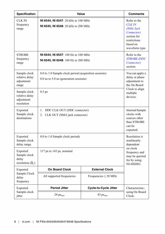
CLK IN frequency range
NI 6544, NI 6547: 20 kHz to 100 MHz
NI 6545, NI 6548: 20 kHz to 200 MHz
Refer to the CLK IN (SMA Jack Connector) section for restrictions based on waveform type.
STROBE frequency range
NI 6544, NI 6547: 100 Hz to 100 MHz
NI 6545, NI 6548: 100 Hz to 200 MHz
Refer to the STROBE (DDC Connector) section.
Sample clock relative delay adjustment range
0.0 to 1.0 Sample clock period (acquisition sessions)
0.0 ns to 5.0 ns (generation sessions)
You can apply a delay or phase adjustment to the On Board Clock to align multiple devices.
Sample clock relative delay adjustment resolution
0.5 ps
Exported Sample clock destinations
1. DDC CLK OUT (DDC connector)2. CLK OUT (SMA jack connector)
Internal Sample clocks with sources other than STROBE can be exported.
Exported Sample clock delay range
0.0 to 1.0 Sample clock periods Resolution is nonlinearly dependent on clock frequency and may be queried for by using NI-HSDIO.
Exported Sample clock delay resolution (δC)
117 ps to 143 ps, nominal
Exported Sample Clock delay frequency
On Board Clock External Clock
All supported frequencies Frequencies ≥ 20 MHz
Exported Sample clock jitter
Period Jitter Cycle-to-Cycle Jitter Characteristic; using On Board Clock.24 psrms 43 psrms
Specification Value Comments
NI PXIe-6544/6545/6547/6548 Specifications | © National Instruments | 9
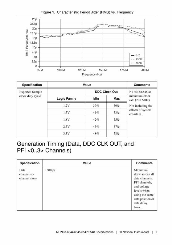
Figure 1. Characteristic Period Jitter (RMS) vs. Frequency
Generation Timing (Data, DDC CLK OUT, and PFI <0..3> Channels)
Specification Value Comments
Exported Sample clock duty cycle
Logic Family
DDC Clock Out NI 6545/6548 at maximum clock rate (200 MHz).
Not including the effects of system crosstalk.
Min Max
1.2V 37% 50%
1.5V 41% 53%
1.8V 42% 55%
2.5V 45% 57%
3.3V 48% 58%
Specification Value Comments
Data channel-to-channel skew
±300 ps Maximum skew across all data channels, PFI channels, and voltage levels when using the same data position or data delay bank.
12.5p
15p
10p
17.5p
7.5p
20p
5p
22.5p
2.5p
25p
075 M 100 M 125 M 150 M 175 M 200 M
Frequency (Hz)
RM
S P
erio
d Ji
tter
(s)
55 °C
25 °C
0 °C
10 | ni.com | NI PXIe-6544/6545/6547/6548 Specifications
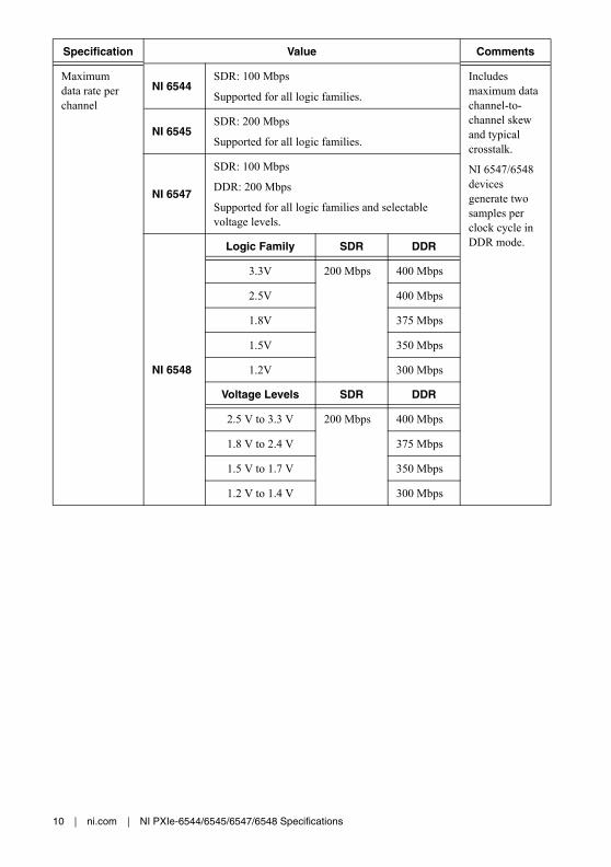
Maximum data rate per channel
NI 6544SDR: 100 Mbps
Supported for all logic families.
Includes maximum data channel-to-channel skew and typical crosstalk.
NI 6547/6548 devices generate two samples per clock cycle in DDR mode.
NI 6545SDR: 200 Mbps
Supported for all logic families.
NI 6547
SDR: 100 Mbps
DDR: 200 Mbps
Supported for all logic families and selectable voltage levels.
NI 6548
Logic Family SDR DDR
3.3V 200 Mbps 400 Mbps
2.5V 400 Mbps
1.8V 375 Mbps
1.5V 350 Mbps
1.2V 300 Mbps
Voltage Levels SDR DDR
2.5 V to 3.3 V 200 Mbps 400 Mbps
1.8 V to 2.4 V 375 Mbps
1.5 V to 1.7 V 350 Mbps
1.2 V to 1.4 V 300 Mbps
Specification Value Comments
NI PXIe-6544/6545/6547/6548 Specifications | © National Instruments | 11
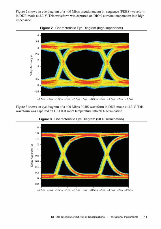
Figure 2 shows an eye diagram of a 400 Mbps pseudorandom bit sequence (PRBS) waveform in DDR mode at 3.3 V. This waveform was captured on DIO 0 at room temperature into high impedance.
Figure 2. Characteristic Eye Diagram (high impedance)
Figure 3 shows an eye diagram of a 400 Mbps PRBS waveform in DDR mode at 3.3 V. This waveform was captured on DIO 0 at room temperature into 50 Ω termination.
Figure 3. Characteristic Eye Diagram (50 Ω Termination)
2
2.5
1.5
3
1
3.5
0.5
4
0
–0.5
–2.5ns –2ns –1.5ns –1ns –0.5ns 0ns –0.5ns –1ns –1.5ns –2ns –2.5ns
Del
ay A
ccur
acy
(s)
0.8
1
0.6
1.2
0.4
1.4
0.2
1.6
0
1.8
–0.2
–2.5ns –2ns –1.5ns –1ns –0.5ns 0ns –0.5ns –1ns –1.5ns –2ns –2.5ns
Del
ay A
ccur
acy
(s)

12 | ni.com | NI PXIe-6544/6545/6547/6548 Specifications
Figure 4. Characteristic Data Delay Accuracy
Specification Value Comments
Data position modes
Sample clock rising edge, Sample clock falling edge, or Delay from Sample clock rising edge
—
Data delay banks
NI 6544/6545: 1 bank for all channels and PFI lines
NI 6547/6548: 3 banks
Bank 0: DIO<0..3>, DIO<16..19>, DIO<28..31>, PFI <0..3>
Bank 1: DIO<4..7>, DIO<20..23>
Bank 2: DIO<8..15>, DIO<24..27>
Multibank data delay is supported only in NI-HSDIO 1.7 and later.
Generation data delay range (δG)
0.0 to 1.0 Sample clock periods Resolution is nonlinearly dependent on clock frequency and may be queried for using NI-HSDIO.
Generation data delay resolution (δG)
117 ps to 143 ps, nominal
Generation data delay frequency
On Board Clock External Clock
All supported frequencies Frequencies ≥ 20 MHz
0
100p
–100p
200p
–200p
300p
–300p
400p
–400p
500p
–500p0 0.1 0.2 0.3 0.4 0.5 0.6 0.7 0.8 0.9 1
Delay Setting
Del
ay A
ccur
acy
(s)
Frequency = 174.00 MHz
Frequency = 101.00 MHz
Frequency = 200.00 MHz
NI PXIe-6544/6545/6547/6548 Specifications | © National Instruments | 13
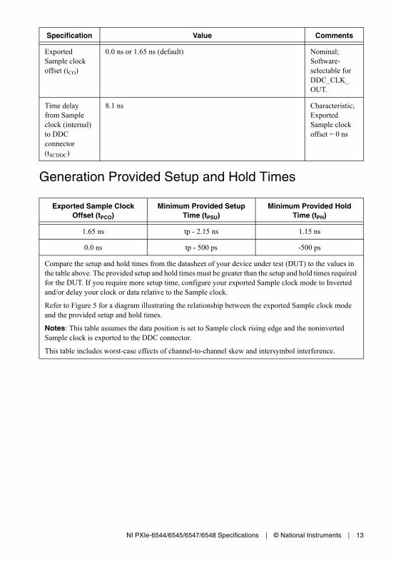
Generation Provided Setup and Hold Times
Specification Value Comments
Exported Sample clock offset (tCO)
0.0 ns or 1.65 ns (default) Nominal; Software- selectable for DDC_CLK_OUT.
Time delay from Sample clock (internal) to DDC connector (tSCDDC)
8.1 ns Characteristic; Exported Sample clock offset = 0 ns
Exported Sample Clock Offset (tPCO)
Minimum Provided Setup Time (tPSU)
Minimum Provided Hold Time (tPH)
1.65 ns tp - 2.15 ns 1.15 ns
0.0 ns tp - 500 ps -500 ps
Compare the setup and hold times from the datasheet of your device under test (DUT) to the values in the table above. The provided setup and hold times must be greater than the setup and hold times required for the DUT. If you require more setup time, configure your exported Sample clock mode to Inverted and/or delay your clock or data relative to the Sample clock.
Refer to Figure 5 for a diagram illustrating the relationship between the exported Sample clock mode and the provided setup and hold times.
Notes: This table assumes the data position is set to Sample clock rising edge and the noninverted Sample clock is exported to the DDC connector.
This table includes worst-case effects of channel-to-channel skew and intersymbol interference.
14 | ni.com | NI PXIe-6544/6545/6547/6548 Specifications
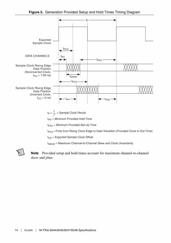
Figure 5. Generation Provided Setup and Hold Times Timing Diagram
Note Provided setup and hold times account for maximum channel-to-channel skew and jitter.
tPSU
tPCO
tP
ExportedSample Clock
DATA CHANNELS
Sample Clock Rising EdgeData Position
(Noninverted Clock,tCO = 1.65 ns)
Sample Clock Rising EdgeData Position
(Inverted Clock,tCO = 0 ns)
tPH
tPH tPSU
tPCO
tSKEW
tP = = Sample Clock Period
tPH = Minimum Provided Hold Time
tPSU = Minimum Provided Set-Up Time
tPCO =Time from Rising Clock Edge to Data Transition (Provided Clock to Out Time)
tCO = Exported Sample Clock Offset
tSKEW = Maximum Channel-to-Channel Skew and Clock Uncertainty
1f
NI PXIe-6544/6545/6547/6548 Specifications | © National Instruments | 15
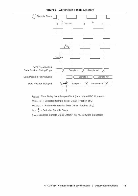
Figure 6. Generation Timing Diagram
tSCDDC : Time Delay from Sample Clock (Internal) to DDC Connector
0 ≤ δC ≤ 1 : Exported Sample Clock Delay (Fraction of tP)
0 ≤ δG ≤ 1 : Pattern Generation Data Delay (Fraction of tP)
tCO = Exported Sample Clock Offset; 1.65 ns, Software-Selectable
DATA CHANNELSData Position Rising Edge
Data Position Falling Edge
Data Position Delayed
Sample Clock
tP = = Period of Sample Clock1ƒ
Sample n Sample n+1
Sample n Sample n+1
Sample n Sample n+1
tSCDDC tP
tCO
δC
δG
Sample n

16 | ni.com | NI PXIe-6544/6545/6547/6548 Specifications
Acquisition Timing (Data, STROBE, and PFI <0..3> Channels)
Specification Value Comments
Channel-to-channel skew
±350 ps Maximum skew across all data channels, PFI channels, and voltage levels when using the same data position or data delay bank.
Maximum data rate per channel
NI 6544SDR: 100 Mbps
Supported for all logic families.
Includes maximum data channel-to-channel skew and typical crosstalk.
NI 6547/6548 devices acquires two samples per clock cycle in DDR mode.
NI 6545SDR: 200 Mbps
Supported for all logic families.
NI 6547
SDR: 100 Mbps
DDR: 200 Mbps
Supported for all logic families and selectable voltage levels.
NI 6548
Logic Family SDR DDR
3.3V 200 Mbps 300 Mbps
2.5V 300 Mbps
1.8V 250 Mbps
1.5V 225 Mbps
1.2V 200 Mbps
Voltage Threshold SDR DDR
1.25 V to 1.65 V 200 Mbps 300 Mbps
0.90 V to 1.20 V 250 Mbps
0.75 V to 0.85 V 225 Mbps
0.60 V to 0.70 V 200 Mbps

NI PXIe-6544/6545/6547/6548 Specifications | © National Instruments | 17
Specification Value Comments
Setup and Hold Times to STROBE
Voltage Threshold
Hold Time (ths) Setup Times (tsus) Characteristic includes maximum data channel-to-channel skew and uncertainty, but does not include system crosstalk. Performance may vary with system crosstalk performance.
<20 MHz ≥20 MHz <20 MHz ≥20 MHz
1.25 V to 1.65 V
2.4 ns 900 ps 2.8 ns 1.15 ns
0.90 V to 1.20 V
1.00 ns 1.20 ns
0.75 V to 0.85 V
1.10 ns 1.40 ns
0.60 V to 0.70 V
1.25 ns 1.75 ns
Data position modes
Sample clock rising edge, Sample clock falling edge, or Delay from Sample clock rising edge.
—
Data delay banks
NI 6544/6545: 1 bank for all channels and PFI lines
NI 6547/6548: 3 banks
Bank 0: DIO<0..3>, DIO<16..19>, DIO<28..31>, PFI <0..3>
Bank 1: DIO<4..7>, DIO<20..23>
Bank 2: DIO<8..15>, DIO<24..27>
Multibank data delay is supported only in NI-HSDIO 1.7 and later.
Acquisition data delay range
0.0 to 1.0 Sample clock periods Resolution is nonlinearly dependent on clock frequency and may be queried for by using NI-HSDIO.
Acquisition data delay resolution
117 ps to 143 ps, nominal
Acquisition data delay frequency
On Board Clock External Clock and STROBE
All supported frequencies Frequencies ≥ 20 MHz

18 | ni.com | NI PXIe-6544/6545/6547/6548 Specifications
Figure 7. Acquisition Timing Diagram Using STROBE as the Sample Clock
Setup time to sample clock (tsusc)
900 ps Nominal; does not include channel-to-channel skew, tDDCSC, or tSCDDC.
Hold time to sample clock (tHSC)
425 ps
Time delay from DDC connector to internal sample clock
6.8 ns Nominal.
Specification Value Comments
DATA CHANNELS
STROBE
STROBE (corrected)*
tSUS
tSUS
tHS tSU
δA
tHS
tSUS = Set-Up Time to STROBE
tHS = Hold Time from STROBE
0 ≤ δA ≤ 1 : Acquisition Data Delay (fraction of tP)
tP = = Sample Clock Period
*Note: When using an external Sample clock greater than 20 MHz, the duty cycle
is corrected to 50%.
1ƒ
Data Position Rising Edge
Data Position Falling Edge
Data Position Delayed
tP

NI PXIe-6544/6545/6547/6548 Specifications | © National Instruments | 19
Figure 8. Acquisition Timing Diagram with Sample Clock Sources Other than STROBE
CLK IN (SMA Jack Connector)
Specification Value Comments
Direction Input to device —
Destinations 1. Reference clock—for the phase lock loop (PLL)2. Sample clock
—
Input coupling AC —
Input protection
±10 VDC Nominal.
tSUSC
tDDCSC : Time Delay from DDC Connector to Internal Sample Clock
0 ≤ δA ≤ 1 : Acquisition Data Delay (fraction of tP)
tP = = Period of Sample Clock
tSUSC = Set-Up Time to Sample Clock
tHSC = Hold Time to Sample Clock
1ƒ
Sample Clock Rising EdgeData Position
Sample Clock Falling EdgeData Position
Delayed from Sample ClockRising Edge Data Position
tP
Internal Sample Clock
tHSC
tSUSC tHSC
DATA CHANNELS
DATA CHANNELS
Virtual Sample ClockProjected to DDC
Connector
δAVirtual Sample Clock
Projected to DDCConnector
tHSC
tSUSC
tHS
20 | ni.com | NI PXIe-6544/6545/6547/6548 Specifications
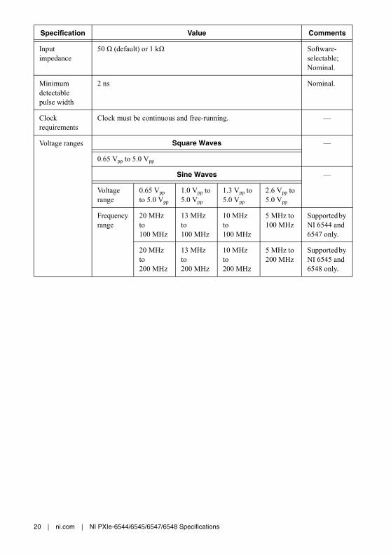
Input impedance
50 Ω (default) or 1 kΩ Software-selectable; Nominal.
Minimum detectable pulse width
2 ns Nominal.
Clock requirements
Clock must be continuous and free-running. —
Voltage ranges Square Waves —
0.65 Vpp to 5.0 Vpp
Sine Waves —
Voltage range
0.65 Vpp to 5.0 Vpp
1.0 Vpp to 5.0 Vpp
1.3 Vpp to 5.0 Vpp
2.6 Vpp to 5.0 Vpp
Frequency range
20 MHz to 100 MHz
13 MHz to 100 MHz
10 MHz to 100 MHz
5 MHz to 100 MHz
Supported by NI 6544 and 6547 only.
20 MHz to 200 MHz
13 MHz to 200 MHz
10 MHz to 200 MHz
5 MHz to 200 MHz
Supported by NI 6545 and 6548 only.
Specification Value Comments

NI PXIe-6544/6545/6547/6548 Specifications | © National Instruments | 21
STROBE (DDC Connector)
As Sample Clock
Frequency range
NI 6544 and NI 6547: 20 kHz to 100 MHz
NI 6545 and NI 6548: 20 kHz to 200 MHz
Nominal 3 dB cutoff point at 100 MHz when using 1 kΩ input impedance.
Duty cycle range
f < 20 MHz: 25% to 75%f ≥ 20 MHz: 40% to 60%
—
As Reference Clock
Reference clock frequency range
5 MHz to 100 MHz (Integer multiples of 1 MHz) —
Reference clock frequency accuracy
± 0.1% Required accuracy of the external Reference clock source.
Reference clock duty cycle
25% to 75% —
Specification Value Comments
Direction Input to device —
Destinations Sample clock (acquisition only) —
STROBE frequency range
NI 6544, NI 6547: 100 Hz to 100 MHz
NI 6545, NI 6548: 100 Hz to 200 MHz
—
STROBE duty cycle range
40% to 60% for clock frequencies ≥ 20 MHz
25% to 75% for clock frequencies < 20 MHz
Note: STROBE duty cycle is corrected to 50% at frequencies ≥ 20 MHz.
Duty cycle at the programmed threshold.
Specification Value Comments
22 | ni.com | NI PXIe-6544/6545/6547/6548 Specifications
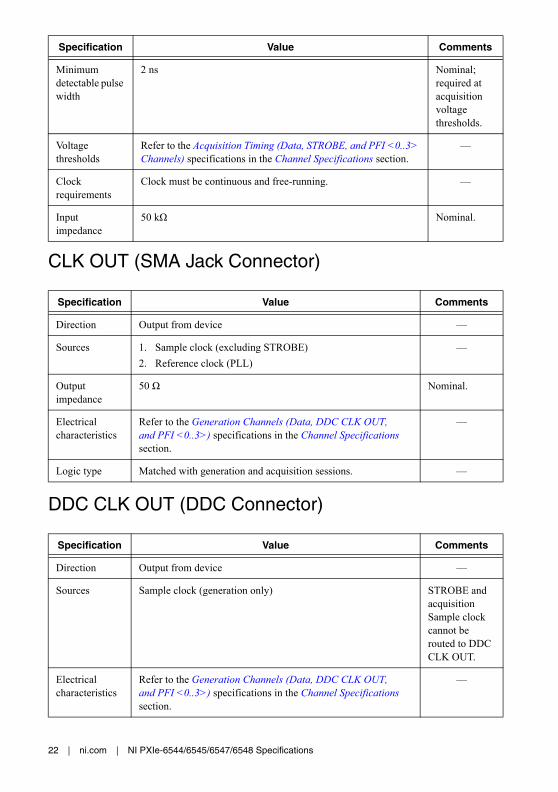
CLK OUT (SMA Jack Connector)
DDC CLK OUT (DDC Connector)
Minimum detectable pulse width
2 ns Nominal; required at acquisition voltage thresholds.
Voltage thresholds
Refer to the Acquisition Timing (Data, STROBE, and PFI <0..3> Channels) specifications in the Channel Specifications section.
—
Clock requirements
Clock must be continuous and free-running. —
Input impedance
50 kΩ Nominal.
Specification Value Comments
Direction Output from device —
Sources 1. Sample clock (excluding STROBE)2. Reference clock (PLL)
—
Output impedance
50 Ω Nominal.
Electrical characteristics
Refer to the Generation Channels (Data, DDC CLK OUT, and PFI <0..3>) specifications in the Channel Specifications section.
—
Logic type Matched with generation and acquisition sessions. —
Specification Value Comments
Direction Output from device —
Sources Sample clock (generation only) STROBE and acquisition Sample clock cannot be routed to DDC CLK OUT.
Electrical characteristics
Refer to the Generation Channels (Data, DDC CLK OUT, and PFI <0..3>) specifications in the Channel Specifications section.
—
Specification Value Comments

NI PXIe-6544/6545/6547/6548 Specifications | © National Instruments | 23
Reference Clock (PLL)
Specification Value Comments
Reference clock sources
1. PXI_CLK100 (PXI Express backplane)2. CLK IN (SMA jack connector)3. None (internal oscillator locked to an internal reference)
Provides the reference frequency for the PLL.
Lock time 150 ms Maximum, not including software latency.
Reference clock frequencies
5 MHz to 100 MHz (integer multiple of 1 MHz) 0.1% required accuracy.
Reference clock duty cycle range
25% to 75% —
Reference clock destinations
CLK OUT (SMA jack connector) —
24 | ni.com | NI PXIe-6544/6545/6547/6548 Specifications
Waveform Specifications
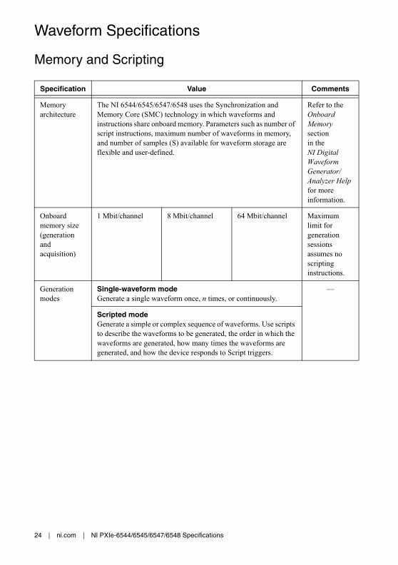
Memory and Scripting
Specification Value Comments
Memory architecture
The NI 6544/6545/6547/6548 uses the Synchronization and Memory Core (SMC) technology in which waveforms and instructions share onboard memory. Parameters such as number of script instructions, maximum number of waveforms in memory, and number of samples (S) available for waveform storage are flexible and user-defined.
Refer to the Onboard Memory section in the NI Digital Waveform Generator/Analyzer Help for more information.
Onboard memory size (generation and acquisition)
1 Mbit/channel 8 Mbit/channel 64 Mbit/channel Maximum limit for generation sessions assumes no scripting instructions.
Generation modes
Single-waveform modeGenerate a single waveform once, n times, or continuously.
—
Scripted modeGenerate a simple or complex sequence of waveforms. Use scripts to describe the waveforms to be generated, the order in which the waveforms are generated, how many times the waveforms are generated, and how the device responds to Script triggers.
NI PXIe-6544/6545/6547/6548 Specifications | © National Instruments | 25
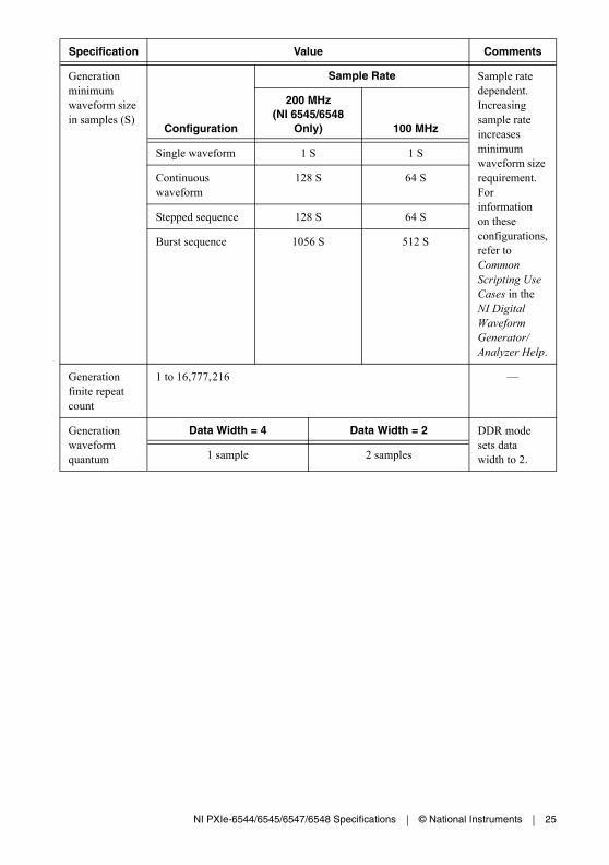
Generation minimum waveform size in samples (S)
Configuration
Sample Rate Sample rate dependent. Increasing sample rate increases minimum waveform size requirement. For information on these configurations, refer to Common Scripting Use Cases in the NI Digital Waveform Generator/Analyzer Help.
200 MHz (NI 6545/6548
Only) 100 MHz
Single waveform 1 S 1 S
Continuous waveform
128 S 64 S
Stepped sequence 128 S 64 S
Burst sequence 1056 S 512 S
Generation finite repeat count
1 to 16,777,216 —
Generation waveform quantum
Data Width = 4 Data Width = 2 DDR mode sets data width to 2.1 sample 2 samples
Specification Value Comments

26 | ni.com | NI PXIe-6544/6545/6547/6548 Specifications
Generation waveform block size(in physical memory)
Data width = 4 Data width = 2 —
32 samples 64 samples
Acquisition minimum record size
1 S Regardless of waveform size, NI-HSDIO allocates at least 640 bytes for a record.
Acquisition record quantum
1 S —
Acquisition maximum number of records
2,147,483,647 Session should fetch fast enough so that unfetched data is not overwritten.
Acquisition number of pre-Reference trigger samples
0 up to full record —
Acquisition number of post-Reference trigger samples
0 up to full record —
Specification Value Comments

NI PXIe-6544/6545/6547/6548 Specifications | © National Instruments | 27
Triggers (Inputs to the NI 6544/6545/6547/6548)
Specification Value Comments
Trigger types 1. Start trigger2. Pause trigger3. Script trigger <0..3> (generation sessions only)4. Reference trigger (acquisition sessions only)5. Advance trigger (acquisition sessions only)6. Stop Trigger (generation sessions only)
—
Sources 1. PFI 0 (SMA jack connector)2. PFI <1..3> (DDC connector)3. PXI_TRIG<0..7> (PXI Express backplane)4. Pattern match (acquisition sessions only)5. Software (user function call)6. Disabled (do not wait for a trigger)
—
Trigger detection
1. Start trigger (edge detection: rising or falling)2. Pause trigger (level detection: high or low)3. Script trigger <0..3> (edge detection: rising or falling;
level detection: high or low)4. Reference trigger (edge detection: rising or falling)5. Advance trigger (edge detection: rising or falling)6. Stop Trigger (edge detection: rising or falling)
—
Minimum required trigger pulse width
15 ns —
Destinations 1. PFI 0 (SMA jack connectors)2. PFI <1..3> (DDC connector)3. PXI_TRIG<0..6> (PXI Express backplane)
Each trigger can be routed to any destination except the Pause trigger. The Pause trigger cannot be exported.
Trigger rearm time Start to
Reference Trigger
Start to Advance Trigger
Advance to Advance Trigger
Reference to
Reference Trigger
Maximum number of samples.
150 s 220 s 220 s 220 s
28 | ni.com | NI PXIe-6544/6545/6547/6548 Specifications
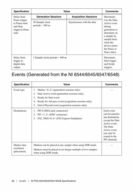
Events (Generated from the NI 6544/6545/6547/6548)
Delay from Pause trigger to Pause state and Stop trigger to Done state
Generation Sessions Acquisition Sessions Maximum; Use the Data Active event during generation to determine on a sample by sample basis when the device enters the Pause or Done states.
50 Sample clock periods + 300 ns
Synchronous with the data
Delay from trigger to digital data output
3 Sample clock periods + 600 ns Maximum; Start trigger and Script triggers.
Specification Value Comments
Event type 1. Marker <0..2> (generation sessions only)2. Data Active event (generation sessions only)3. Ready for Start event4. Ready for Advance event (acquisition sessions only)5. End of Record event (acquisition sessions only)
—
Destinations 1. PFI 0 (SMA jack connectors)2. PFI <1..3> (DDC connector)3. PXI_TRIG<0..6> (PXI Express backplane)
Each event can be routed to any destination, except the Data Active event. The Data Active event can only be routed to the PFI channels.
Marker time resolution (placement)
Markers can be placed at any sample when using SDR mode.
Markers must be placed at an integer multiple of two samples when using DDR mode.
—
Specification Value Comments
NI PXIe-6544/6545/6547/6548 Specifications | © National Instruments | 29
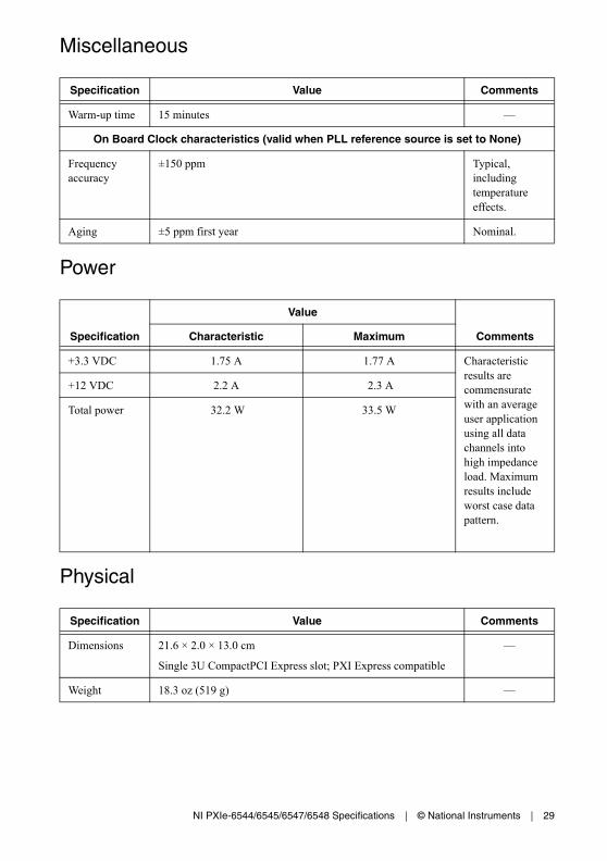
Miscellaneous
Power
Physical
Specification Value Comments
Warm-up time 15 minutes —
On Board Clock characteristics (valid when PLL reference source is set to None)
Frequency accuracy
±150 ppm Typical, including temperature effects.
Aging ±5 ppm first year Nominal.
Specification
Value
CommentsCharacteristic Maximum
+3.3 VDC 1.75 A 1.77 A Characteristic results are commensurate with an average user application using all data channels into high impedance load. Maximum results include worst case data pattern.
+12 VDC 2.2 A 2.3 A
Total power 32.2 W 33.5 W
Specification Value Comments
Dimensions 21.6 × 2.0 × 13.0 cm
Single 3U CompactPCI Express slot; PXI Express compatible
—
Weight 18.3 oz (519 g) —

30 | ni.com | NI PXIe-6544/6545/6547/6548 Specifications
I/O Panel Connectors
Software
Label Function(s)Connector
Type
CLK IN External Sample clock, external Reference clock. SMA jack
PFI 0 Events, triggers. SMA jack
CLK OUT External Sample clock, exported Reference clock. SMA jack
Digital Data & Control (DDC)
Digital data channels, exported Sample clock, STROBE, events, triggers.
68pin VHDCI
Specification Value Comments
Driver software NI-HSDIO driver software 1.6 or later. NI-HSDIO allows you to configure and control the NI 6544/6545/6547/6548. NI-HSDIO provides application interfaces for many development environments. NI-HSDIO follows IVI application programming interface (API) guidelines.
Hardware compare, per cycle tristate, and multibank data delay are supported only in NI-HSDIO 1.7 or later.
—
Application software
NI-HSDIO provides programming interfaces for the following application development environments (ADEs):• National Instruments LabVIEW• National Instruments LabWindows™/CVI™
• Microsoft Visual C/C++
Refer to the NI-HSDIO Instrument Driver Readme for more information about supported ADE versions.
Test panel National Instruments Measurement & Automation Explorer (MAX) provides test panels with basic acquisition and generation functionality for the NI 6544/6545/6547/6548. MAX is included on the NI-HSDIO driver CD.
—
NI PXIe-6544/6545/6547/6548 Specifications | © National Instruments | 31
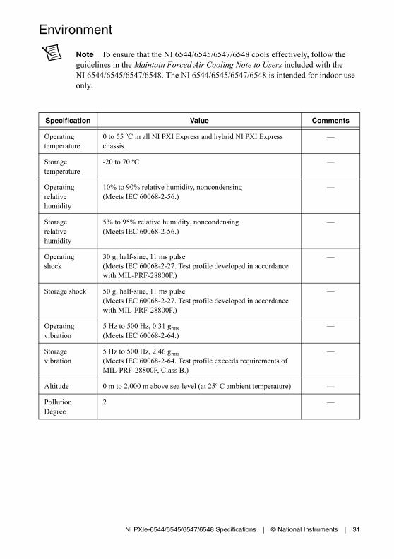
Environment
Note To ensure that the NI 6544/6545/6547/6548 cools effectively, follow the guidelines in the Maintain Forced Air Cooling Note to Users included with the NI 6544/6545/6547/6548. The NI 6544/6545/6547/6548 is intended for indoor use only.
Specification Value Comments
Operating temperature
0 to 55 ºC in all NI PXI Express and hybrid NI PXI Express chassis.
—
Storage temperature
-20 to 70 ºC —
Operating relative humidity
10% to 90% relative humidity, noncondensing (Meets IEC 60068-2-56.)
—
Storage relative humidity
5% to 95% relative humidity, noncondensing (Meets IEC 60068-2-56.)
—
Operating shock
30 g, half-sine, 11 ms pulse (Meets IEC 60068-2-27. Test profile developed in accordance with MIL-PRF-28800F.)
—
Storage shock 50 g, half-sine, 11 ms pulse (Meets IEC 60068-2-27. Test profile developed in accordance with MIL-PRF-28800F.)
—
Operating vibration
5 Hz to 500 Hz, 0.31 grms (Meets IEC 60068-2-64.)
—
Storage vibration
5 Hz to 500 Hz, 2.46 grms (Meets IEC 60068-2-64. Test profile exceeds requirements of MIL-PRF-28800F, Class B.)
—
Altitude 0 m to 2,000 m above sea level (at 25º C ambient temperature) —
Pollution Degree
2 —

32 | ni.com | NI PXIe-6544/6545/6547/6548 Specifications
Safety, Electromagnetic Compatibility, and CE Compliance
Specification Value Comments
Safety The NI 6544/6545/6547/6548 meets the requirements of the following standards of safety for electrical equipment for measurement, control, and laboratory use:• IEC 61010-1, EN 61010-1• UL 61010-1, CSA 61010-1
For UL and other safety certifications, refer to the product label or visit ni.com/certification, search by model number or product line, and click the appropriate link in the Certification column.
Electromagnetic Compatibility
The NI 6544/6545/6547/6548 meets the requirements of the following EMC standards for electrical equipment for measurement, control, and laboratory use:
EN 61326-1 (IEC 61326-1): Class A emissions, Basic immunity
EN 55011 (CISPR 11): Group 1, Class A emissions
AS/NZS CISPR 11: Group 1, Class A emissions
FCC 47 CFR Part 15B: Class A emissions
ICES-001: Class A emissions
For the standards applied to assess the EMC of this product, refer to the Online Product Certification section below.
To meet EMC compliance the following cautions apply.
Note: SHC68-C68-D4 or SHC68-C68-D2 shielded cable and provided cable ferrites must be used when operating the NI 6544/6545/6547/6548.
Note: EMI filler panels (NI P/N 778700-01) must be installed in all empty slots of the NI 6544/6545/6547/6548.
CE Compliance This product meets the essential requirements of applicable European Directives, as amended for CE marking, as follows:
2006/95/EC; Low-Voltage Directive (safety)
2004/108/EC; Electromagnetic CompatibilityDirective (EMC)
—
Online Product Certification
Refer to the product Declaration of Conformity (DoC) for additional regulatory compliance information. To obtain product certifications and the DoC for this product, visit ni.com/certification, search by model number or product line, and click the appropriate link in the Certification column.
—
NI PXIe-6544/6545/6547/6548 Specifications | © National Instruments | 33
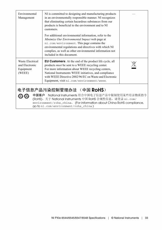
Environmental Management
NI is committed to designing and manufacturing products in an environmentally responsible manner. NI recognizes that eliminating certain hazardous substances from our products is beneficial to the environment and to NI customers.
For additional environmental information, refer to the Minimize Our Environmental Impact web page at ni.com/environment. This page contains the environmental regulations and directives with which NI complies, as well as other environmental information not included in this document.
—
Waste Electrical and Electronic Equipment (WEEE)
EU Customers: At the end of the product life cycle, all products must be sent to a WEEE recycling center. For more information about WEEE recycling centers, National Instruments WEEE initiatives, and compliance with WEEE Directive 2002/96/EC on Waste and Electronic Equipment, visit ni.com/environment/weee.
RoHSNational Instruments
(RoHS) National Instruments RoHS ni.com/environment/rohs_china (For information about China RoHS compliance, go to ni.com/environment/rohs_china.)

© 2009–2014 National Instruments. All rights reserved.
374962E Mar14
Refer to the NI Trademarks and Logo Guidelines at ni.com/trademarks for more information on National Instruments trademarks. Other product and company names mentioned herein are trademarks or trade names of their respective companies. For patents covering National Instruments products/technology, refer to the appropriate location: Help»Patents in your software, the patents.txt file on your media, or the National Instruments Patents Notice at ni.com/patents. You can find information about end-user license agreements (EULAs) and third-party legal notices in the readme file for your NI product. Refer to the Export Compliance Information at ni.com/legal/export-compliance for the National Instruments global trade compliance policy and how to obtain relevant HTS codes, ECCNs, and other import/export data.