spectra engineering pty ltd - fcc id search engineering pty ltd . base station, repeater, ... 3.16...
TRANSCRIPT

SPECTRA ENGINEERING Pty Ltd
Base Station, Repeater, Receiver and Transmitter
MX800
Technical Manual


Technical Manual MX800 Transceiver
Spectra Engineering Pty Ltd
ABN 65 057 696 438
9 Trade Road Malaga
Western Australia 6090
Tel: +61-8-92482755 Fax: +61-8-92482756
Email: [email protected] Web: www.spectraeng.com.au
Manual Revision 4.3.1 May 2008
In order to continually improve our products, Spectra Engineering Pty Ltd reserves the right to alter, without notice and at any time, the equipment and specifications described in this document.
All performance figures quoted are typical and are subject to normal manufacturing and service tolerances.
The purchaser is warned that statements made in this document may be inaccurate due to typographical or other errors or subsequent modifications of the product. While every care has been taken in the creation of this document, no warranty of accuracy or reliability is given, in any advice or information contained in this document. The responsibility for any loss or damage whatsoever arising in any way or any representation, act or omission whether express or implied (including responsibility to any person by reason of negligence) is not accepted by Spectra Engineering Pty Ltd or any director, officer, agent or employee of Spectra Engineering Pty Ltd.
Copyright © Spectra Engineering Pty Ltd 1997-2008
This work is copyright. Other than as permitted by Law, no part of it may be reproduced, stored in a retrieval system or transmitted in any form or by any process without prior written permission.
Regulatory Information
Federal Communications Commission (FCC) Interference Warning. Note: The equipment has been tested and found to comply with the limits for a class B digital device, pursuant to Part 15 of the FCC Rules..
Radio And Telecommunications Terminal Equipment (R&TTE) Directive insures the protection of health and safety of users, as well as electromagnetic compatibility. Please see Declarations of Conformity or specification sheet for approved bands and test standards. These standards & limits are designed to provide reasonable protection against harmful interference when the equipment is operated in a commercial or residential environment. This equipment generates, uses and can radiate radio frequency energy. If not installed and used in accordance with this instruction manual, may cause harmful interference to radio communication.
© SPECTRA ENGINEERING 2008 Revision 4.3.1B i

MX800 Transceiver Technical Manual
This page left blank intentionally
© SPECTRA ENGINEERING 2008 Revision 4.3.1B ii

Technical Manual MX800 Transceiver
© SPECTRA ENGINEERING 2008 Revision 4.3.1B iii
Record Of Changes Any changes to this manual are recorded on this list. Spectra Engineering may issue replacement pages to you from time to time. If any updates are issued, you will also receive a replacement for this page.
Date Version Chapter Changes Pages Changed
April 1998 2.0 General Revision All
May 1998 2.01 Minor corrections i,ii,iii,10,15
May 1998 2.02 Master doc All
Oct 1998 2.03 Minor Corrections i,ii,9,27,29,30,35
April 1999 3.0 Local control features added All
Dec 1999 3.1 Options chapter added All
June 2000 4.0 Document reformatted All
Aug 2000 4.01 MX800 Configuration Guide 70
Nov 2000 4.1 Minor Revision All
Sept 2001 4.1.1 Minor Revisions All
Sept 2002 4.1.2 Minor Revisions 15,71,82,90,92,96
Jan 2003 4.1.3 Minor Corrections 22,25,40,71
June 2004 4.1.4 Minor Revision
August 04 4.2.0 Revisions All
Oct 04 4.2.1 Minor Revision 56
Nov 05 4.2.2 Minor Revision All
Add T19/26 Micro Drawing
Add RV1 to TX alignment 73-75
30/03/06 Updated Binary bits in table. 95
21/04/06 Updated options section
16-Nov-06 4.2.3 Added screw type section 12
22 May. 07 4.2.4 Added T36 option.
Jan 2008 4.2.5 Additions to Regulatory Information, Safety Summary, Installation and Operation sections.
I, V,11
Mar2008 4.3.0 New Software manual print version . Contains only basic options. T19 & T36 removed
May 2008 4.3.1 Changes to default DIP2 switch settings.

MX800 Transceiver Technical Manual
© SPECTRA ENGINEERING 2008 Revision 4.3.1B iv

Technical Manual MX800 Transceiver
© SPECTRA ENGINEERING 2008 Revision 4.3.1B v
SAFETY SUMMARY Although there are no dangerous mains voltages present within the equipment, the following general safety precautions as would normally apply, should be observed during all phases of operation, service and repair of this equipment.
AROUND THE EQUIPMENT To minimise any possible shock hazard from an external power supply or lightning strike, the chassis or equipment cabinet must be connected to an electrical ground.
To minimise any possible shock hazard from an external power supply or lightning strike, the chassis & equipment cabinet must be connected to an electrical ground.
A threaded grounding screw terminal is provided on the left-hand side of the radio chassis for connection to the site ground point (Protective Earth).
Provide adequate ventilation around the rear of the equipment.
DO NOT OPERATE IN AN EXPLOSIVE ATMOSPHERE Do not operate the equipment in the presence of flammable gases or fumes. Operation of any electrical equipment in such an environment constitutes a definite safety hazard.
DO NOT ATTEMPT INTERNAL SERVICE WHILE TRANSMITTING Thermal or RF burns may result from touching certain components within the power amplifier module while transmitting or operating the transmitter.
DO NOT SUBSTITUTE PARTS OR MODIFY THE EQUIPMENT Because of the danger of introducing additional hazards, do not install substitute or lower voltage parts to the equipment. Return to your authorised distributor.
EXERCISE CAUTION AND CORRECT DISPOSAL OF RF POWER DEVICES Most RF power transistors and some RF power hybrids contain Beryllium Oxide. Although they are normally safe, if physically damaged toxic dust may be released. Consult your local authority for correct disposal thereof.
WARRANTY CONDITIONS & PRECAUTIONS The following conditions are not covered by the warranty of the MX800. Please ensure that the MX800 is not subject to;
1. Over voltage or Reverse Power Supply Voltage.
2. Operation in locations subject to abnormal environmental conditions such as extreme temperatures or ingress of moisture.
3. Operation of the MX800 Transmitter output into an open or short circuit or an incorrectly terminated load.

MX800 Transceiver Table of Contents
Table of Contents 1. General Description ................................................................................ 1
1.1 Physical Description ..................................................................... 3 1.1.1 Front Panel ..................................................................... 3 1.1.1 Rear Panel ....................................................................... 6 1.1.2 Side Panel ........................................................................ 7
1.2 Module Functional Description .................................................... 7 1.2.1 Exciter Module ................................................................ 7 1.2.2 Receiver Module .............................................................. 8 1.2.3 Power Amplifier Module ................................................. 8 1.2.4 Micro Controller Board .................................................. 9
2. Installation and Operation ................................................................... 11 2.1 Installation .................................................................................. 11 2.2 Screw Head Types ...................................................................... 12 2.3 Operation .................................................................................... 13
2.3.1 MXTOOLS Utility .......................................................... 13 2.3.2 Setting to Work .............................................................. 14 2.3.3 Adjustments ................................................................... 19
3. Options ................................................................................................... 21 3.1 T01 Programmable Channel Spacing ......................................... 21
3.1.1 Description .................................................................... 21 3.1.2 Installation .................................................................... 21
3.2 T02 Programmable CTCSS encoder/decoder ............................ 22 3.2.1 Description .................................................................... 22 3.2.2 Installation .................................................................... 22
3.3 T03 Programmable DCS/CTCSS encoder/decoder .................... 23 3.3.1 Description .................................................................... 23 3.3.2 Installation .................................................................... 23
3.4 T05 Balanced and Isolated VF plus E&M ................................. 25 3.4.1 Description .................................................................... 25 3.4.2 Installation .................................................................... 26
3.5 T06 Simplex Changeover Relay................................................. 28 3.5.1 Description .................................................................... 28 3.5.2 Installation .................................................................... 29
3.6 T08 VF Delay ............................................................................. 31 3.6.1 Description .................................................................... 31 3.6.2 Installation .................................................................... 32
3.7 T09 300Hz Upgrade HPF Filter ................................................. 33 3.7.1 Description .................................................................... 33 3.7.2 Installation .................................................................... 34
3.8 T10 Power Save Mode ............................................................... 35
© SPECTRA ENGINEERING 2008 Revision 4.3.1B vi

Technical Manual Table of Contents
3.10.1 Description ...................................................................... 35 3.10.2 Installation .................................................................... 37
3.9 T11 Combined Options .............................................................. 38 3.10 T12 External Reference Oscillator Input .................................... 38
3.12.1 Description .................................................................... 38 3.12.2 Installation .................................................................... 39
3.11 T13 Local Speaker, Mic Socket and Front Panel Mute.............. 41 3.11.1 Description .................................................................... 41 3.11.2 Installation .................................................................... 42
3.12 T14 Local Channel Change ........................................................ 45 3.12.1 Description .................................................................... 45 3.12.2 Installation .................................................................... 45
3.13 T16 1PPM Frequency Stability .................................................. 47 3.14 U69 Extended Temperature Range Verification ........................ 47 3.15 T19/26 Line Interface Board. ..................................................... 47 3.16 T29 Balanced and Isolated VF plus E&M ................................. 48 3.17 T31 Network Adapter ................................................................. 50
3.17.1 Optional Dongles .......................................................... 50 3.17.2 U71 Dongle ................................................................... 51 3.17.3 U72 Dongle ................................................................... 51 3.17.4 U73 Dongle with Digital IO Port Replicator ................ 51
3.18 T34 Ethernet option .................................................................... 52 3.19 T36 Option - TX Ref Oscillator input and Modulator ............... 52
4. Technical Description ........................................................................... 55 4.1 Exciter Module ........................................................................... 55 4.2 Receiver Module ........................................................................ 56 4.3 Power Amplifier Module ........................................................... 57 4.4 Micro Controller Board .............................................................. 58
4.4.1 Overall Radio Management .......................................... 58 4.4.2 TX Signal Processing .................................................... 59 4.4.3 RX Signal Processing .................................................... 60 4.4.4 RF Power Control ......................................................... 60 4.4.5 User Interface ................................................................ 61
5. Alignment and Testing .......................................................................... 63 5.1 Transceiver Setup, Calibration and Alignment .......................... 63
5.1.1 Sending Model Number and Serial Number to the Radio ............................................................................. 63
5.1.2 Sending Configuration Information .............................. 63 5.1.3 Sending Channel Information ....................................... 64 5.1.4 Setting Alignment Channel ............................................ 64 5.1.5 Power Calibration ......................................................... 64 5.1.6 RSSI Calibration ........................................................... 65
© SPECTRA ENGINEERING 2008 Revision 4.3.1B vii

MX800 Transceiver Table of Contents
5.1.7 Temperature Calibration ............................................... 65 5.1.8 TX Power Adjustment .................................................... 65 5.1.9 Peak Deviation and Modulation Balance ..................... 66 5.1.10 TX Centre Frequency Alignment ................................... 67 5.1.11 TX Line Input Level and Nominal Deviation
Alignment ...................................................................... 68 5.1.12 RX Line Output Level Adjustment ................................. 70 5.1.13 TX VF Loop Back Level ................................................ 70 5.1.14 Mute Threshold Setting ................................................. 70
5.2 Module Level Test Procedures ................................................... 71 5.2.1 Exciter Module .............................................................. 71 5.2.2 Receiver Module ............................................................ 72 5.2.3 Power Amplifier Module ............................................... 74 5.2.4 VCO Board .................................................................... 75 5.2.5 Microcontroller Module ................................................ 75
6. MX800 Base Station Fault Finding Procedure ................................... 77 6.1 MX800 Base Station .................................................................. 77
6.1.1 Transmitter Section ....................................................... 77 6.1.2 Receiver Section ............................................................ 78
6.2 Microcontroller PCB .................................................................. 79 6.3 Receiver Module ........................................................................ 79
6.3.1 VCO Locking. ................................................................ 79 6.3.2 RX Front End ................................................................ 79
6.4 IF Section ................................................................................... 80 6.5 Exciter Module ........................................................................... 80
6.5.1 VCO Locking. ................................................................ 80 6.5.2 RF Power ...................................................................... 81
6.6 Power Amplifier ......................................................................... 81
7. Appendices ............................................................................................. 83 7.1 MX800 Interface Connections ................................................... 83
7.1.1 CN1 DB15 Female Line I/O Connector ........................ 84 7.2 CN2 DB9 Female Monitor Connector ....................................... 86 7.3 CN3 DB25 Female Digital I/O Connector ................................. 87
7.3.1 CN4 DB9 Male RS232 Connector ................................. 88 7.3.2 CN6 Simplex Relay/External Reference ........................ 88 7.3.3 CN7 RX Input ................................................................ 89 7.3.4 CN8 TX Output .............................................................. 89 7.3.5 CN9 RJ45 ...................................................................... 89 7.3.6 CN5 DC Power Input .................................................... 89
7.4 MX800 Specifications ................................................................ 90 7.4.1 Operating Frequency Bands ......................................... 90 7.4.2 General .......................................................................... 90
© SPECTRA ENGINEERING 2008 Revision 4.3.1B viii

Technical Manual Table of Contents
7.4.3 Transmit ........................................................................ 91 7.4.4 Receive .......................................................................... 92 7.4.5 Ancillaries ..................................................................... 93
7.5 Channel Select DIP Switch Settings .......................................... 93 7.6 MX800 Model Number Configuration Guide ............................ 97 7.7 MX800 System Applications ..................................................... 98
7.7.1 Conventional base station/repeater .............................. 98 7.7.2 Link transceiver ............................................................. 99 7.7.3 Data transceiver ............................................................ 99 7.7.4 Paging transmitter ........................................................ 99 7.7.5 Trunking Base Station ................................................. 100 7.7.6 Systems base ................................................................ 100 7.7.7 Repeater with Morse ID .............................................. 100 7.7.8 Simplex base station .................................................... 100 7.7.9 Duplicated base station ............................................... 101 7.7.10 Power Save base station .............................................. 101 7.7.11 Tone key base station .................................................. 101 7.7.12 Voting base station ...................................................... 101 7.7.13 Simulcast base station ................................................. 101
8. Superseded Technical Information .................................................... 109 8.1 Power Amplifier Module ......................................................... 109
8.1.1 Technical Description ................................................. 109 8.1.2 PA Module Test Procedure ......................................... 109 8.1.3 PA Fault Finding Procedure ....................................... 111
9. Drawings .............................................................................................. 113 9.1 Superseded Drawings ............................................................... 114
© SPECTRA ENGINEERING 2008 Revision 4.3.1B ix

MX800 Transceiver Table of Contents
List of Tables Table 1-1 LED Functions ........................................................................................... 3 Table 1-2 Rear Panel Connections ............................................................................. 6 Table 2-1 Micro Controller Jumpers ........................................................................ 16 Table 2-2 DIP Switch 2 Settings ............................................................................... 17 Table 2-3 Power Control Function Settings ............................................................. 19 Table 3-1 CN9 Connections ...................................................................................... 26 Table 3-2 Option PCB Link Settings ......................................................................... 32 Table 3-3 Option PCB Link Settings ......................................................................... 34 Table 3-4 Current Consumption Details ................................................................... 36 Table 3-5 Option PCB Link Settings ......................................................................... 36 Table 3-6 MX800 Mic Socket Pinout ........................................................................ 42 Table 3-7 T29 RJ45 Pin outs. .................................................................................... 49 Table 3-8 T29 Factory Default Jumper Setting. ........................................................ 49 Table 4-1 Microprocessor Port Parameters ............................................................. 58 Table 5-1 Peak Deviation Settings ............................................................................ 66 Table 5-2 Nominal Deviation ................................................................................... 68 Table 7-1 MX800 Interface Connectors ................................................................... 83 Table 7-2 CN1 Connections ...................................................................................... 85 Table 7-3 CN2 Connections ...................................................................................... 86 Table 7-4 CN3 Connections ...................................................................................... 87 Table 7-5 CN4 Connector Jumpers .......................................................................... 88 Table 7-6 CN5 DC Power Input Connections .......................................................... 89 Table 7-7 General Specifications.............................................................................. 91 Table 7-8 Transmit Specifications ............................................................................ 91 Table 7-9 Receive Specification ................................................................................ 92 Table 7-10 Ancilary Specifications ........................................................................... 93 Table 9-1 Drawings ................................................................................................ 114
© SPECTRA ENGINEERING 2008 Revision 4.3.1B x

Technical Manual Table of Contents
List of Figures Figure 1-1 Standard Front Panel ............................................................................... 4 Figure 1-2 Local Control Front Panel ....................................................................... 4 Figure 1-3 MX800 Rear Panel ................................................................................... 6 Figure 1-4 MX800 Side Panel .................................................................................... 7 Figure 3-1 MX800 T01 Option, Programable bandwidth fitted to RX module. ........ 21 Figure 3-2MX800 DCS Option T03 ........................................................................... 23 Figure 3-3 MX800 Option T05 Balanced & Isolated VF I/O with E&M leads ......... 25 Figure 3-4 CN9 RJ45 Pin-out Detail (View from Rear of MX800) .......................... 26 Figure 3-5 T06 Simplex Changeover Relay ............................................................... 28 Figure 3-6MX800 T08,T09,T10 Option board complete ........................................... 31 Figure 3-7 Front Panel with Speaker, Mic and Mute ............................................... 41 Figure 3-8 RJ45 socket viewed from front of MX800 ............................................... 42 Figure 3-9 MX800 T29 otpion board ........................................................................ 48 Figure 3-10 CN9 RJ45 Pin-out Detail (View from Rear of MX800) ......................... 49 Figure 3-11 T31 Option Board .................................................................................. 50 Figure 3-12 U72/U71 Dongle .................................................................................... 51 Figure 3-13 U73 Dongle............................................................................................ 51 Figure 4-1 MX800 Top View .................................................................................... 55 Figure 5-1 Under (increase level) ............................................................................ 67 Figure 5-2 Over (decrease level) .............................................................................. 67 Figure 5-3 Correctly Aligned Waveform .................................................................. 67 Figure 7-1 CN5 DC Input (View from rear of MX800) ............................................ 89 Figure 7-2 MX800’s Setup in system rack ................................................................. 98 Figure 9-1 Receiver Component Overlay ............................................................... 115 Figure 9-2 Exciter Component Overlay ................................................................. 116 Figure 9-3 PA Component Overlay - Superseded Version ..................................... 117 Figure 9-4 PA Component Overlay –New Wide Band PA Version ......................... 117 Figure 9-5 Micro Controller Component Overlay (Rev P4) .................................. 118 Figure 9-6 Tx and Rx VCO Component Overlay Bands A to Q3 ........................... 119 Figure 9-7 Tx and Rx VCO Component Overlay Bands R to X .............................. 119 Figure 9-8 HP Rx VCO Component Overlay Bands A to Q ................................... 120 Figure 9-9 TX/RX V3 VCO Component Overlay .................................................... 120
© SPECTRA ENGINEERING 2008 Revision 4.3.1B xi


Technical Manual
1. General Description The MX800 series employs state of the art design and construction methods to deliver a range of high performance, ultra reliable radio transceivers. They are ideally suited for use in VHF or UHF two way voice radio systems, however, the MX800 can perform in a range of applications where the added advantage of linear frequency and phase response from DC to 3.4 kHz can be utilised. The MX800 uses a two-point modulation method synthesiser for extended low end VF transmit frequency response. The Receiver, Exciter and Power Amplifier are contained in their own specialised aluminium module and can be easily removed from the main chassis.
The flexibility of the MX800 series allows it to be configured for a wide range of applications.
Standard MX800 applications include:
Conventional 2-Way voice base station
Full duplex or simplex base station
Radio modem base station
Direct FSK or SELCALL baseband repeater
Trunking base station for MPT1327, LTR, SmartTrunk and others
Analog Cellular base station
POCSAG paging transmitter to 2400 BPS
POCSAG repeater
DC-coupled Direct FSK modulation system
Voice repeater
Wide band data repeater
DC-coupled repeater
Point to point link
Fast 25mS repeater for multi hopping
Cross band link or repeater
Simulcast transmitter
Quasi-Sync offset transmitter
© SPECTRA ENGINEERING 2008 Revision 4.3.1B 1

MX800 Transceiver General Description
The MX800 incorporates special technical features, of which the key ones are listed below:
Extremely low conducted emissions
Extremely low transmitter spurious
Fast transmitter on time
Transmitter frequency response down to DC
Low group delay distortion
Very Wide RF switching bandwidth
No re-tune receiver or transmitter
Fully software programmable
Built in diagnostics
Trunking control and VF routing interface
Built in community multi-tone style repeater
High stability reference input for Simulcast systems
In addition, the MX800 can be fitted with many options, not being limited to the following:
Programmable channel spacing
Programmable CTCSS / DCS encoder and decoder
Isolated VF and E&M lead interfaces
Simplex antenna changeover relay
VF audio delay for noiseless mute/squelch/repeater function
Low receiver standby current consumption
External reference oscillator input
Local speaker and microphone
Push wheel channel selector
High stability options
Audio Facilities board covers many new features
Internal Modem or Ethernet interface
Special high performance receiver options
Other custom features on special request
For further information, please contact Spectra Engineering.
© SPECTRA ENGINEERING 2008 Revision 4.3.1B 2

Technical Manual General Description
© SPECTRA ENGINEERING 2008 Revision 4.3.1B 3
1.1 Physical Description The MX800 is a compact lightweight standard 19" rack mounting transceiver. It is designed to mount horizontally in a 19" rack frame and occupies 2RU (89mm). The depth of the unit is 330mm and the weight is less than 9kg.
The unit consists of four main sub assemblies an Exciter Module, a Receiver Module, a Power Amplifier Module and a Micro Controller board. These modules are housed in a fully welded steel case.
The MX800 features a high degree of RFI and EMI screening throughout the design and construction. The receiver and exciter (low power transmitter) modules are contained in solid aluminium enclosures, and for additional screening each interface pin in the modules is individually filtered. The PA module is contained in a special compact efficient extrusion for minimum harmonic radiation. This design results in low conducted and radiated emissions and minimal susceptibility to RFI and EMI.
User interface is via the front and rear panels. The rear panel provides access to all connectors and the standard front panel provides 6 LED indicators of the radio status. The local control option front panel has additional speaker, microphone and (optionally) channel select functions. Other variations can accommodate serial and monitor ports, as well as VF line level adjustment on the front panel.
1.1.1 Front Panel
1.1.1.1 Standard Front Panel
The MX800 standard front panel is illustrated below. Custom versions of the front panel can be supplied to OEM customers.
Table 1-1 below explains the functions of the front panel LED's. Each LED indicates the status of the MX800 in real time.
LED FUNCTION
POWER Indicates the power supply voltage is within software selectable limits.
RX The receiver is receiving a signal or the receiver’s squelch is open.
TX The transmitter is transmitting RF power.
CTCSS A valid Continuous Tone Coded Squelch Signal has been detected.
AUX An Aux function is selected or the PLL is unlocked.
ALARM A prearranged alarm condition exists.
Table 1-1 LED Functions

MX800 Transceiver General Description
© SPECTRA ENGINEERING 2008 Revision 4.3.1B 4
Figure 1-1 Standard Front Panel
1.1.1.2 Local Control Front Panel
The Local Control Front Panel is illustrated in Figure 1-2 below. The Local Control Front Panel is illustrated in
Figure 1-2 Local Control Front Panel Figure 1-2 Local Control Front Panel
It has the same LED indicators as the standard front panel as well as the following features It has the same LED indicators as the standard front panel as well as the following features
Loudspeaker and Volume Control A 1 Watt loudspeaker is provided to monitor 'on air' received audio as well as transmit audio from line. Volume control is provided by means of a potentiometer or a 3-position toggle switch adjacent to the loudspeaker. This switch is biased in the centre position. To raise or lower the volume the switch is momentarily moved up or down respectively. For each switch closure the volume is incremented or decremented a fixed amount. Newer versions of the MX800 Micro Controller PCB support a conventional rotary volume control. The newer versions are also backward compatible in that the circuitry can still support the older up/down control method as well as the new chassis can still accommodate the older revision board. The speaker has a link selectable connection to a tone output from the microcontroller. This may be used in conjunction with the appropriate software configuration to generate an alert tone to the user.
Loudspeaker and Volume Control A 1 Watt loudspeaker is provided to monitor 'on air' received audio as well as transmit audio from line. Volume control is provided by means of a potentiometer or a 3-position toggle switch adjacent to the loudspeaker. This switch is biased in the centre position. To raise or lower the volume the switch is momentarily moved up or down respectively. For each switch closure the volume is incremented or decremented a fixed amount. Newer versions of the MX800 Micro Controller PCB support a conventional rotary volume control. The newer versions are also backward compatible in that the circuitry can still support the older up/down control method as well as the new chassis can still accommodate the older revision board. The speaker has a link selectable connection to a tone output from the microcontroller. This may be used in conjunction with the appropriate software configuration to generate an alert tone to the user.
Figure 1-2 below.
Power
RX
TX
CTCSS
Aux
Alarm
RS232 Port ole
heelhange
Line I/P Adjust H
Push-wChannel C
Speaker
VolumeControl
RJ45Microphone
Socket
SquelchAdjust Hole
/PLine OAdjust Hole

Technical Manual General Description
Microphone Socket An RJ45 socket is provided on the front panel for connection of a microphone.
Channel Change Control Twin push-wheel switches can be optionally fitted to the front panel to allow selection of the operating channel. This switch replaces the channel select function normally accessible on CN3 on the rear panel. 100 channels are selectable. Refer to section 2.3.2.3 for channel select method.
RS232 and Monitor Ports Provision is made to optionally fit these two connectors on the front panel instead of on the rear panel. The pin-out and functions of these two ports remain unchanged when this is done.
Mute / Squelch Adjustment Provision is made to optionally locate the mute / squelch control potentiometer behind the front panel. A screwdriver hole is provided in the front panel to access this adjustment.
Line Level Adjustments Provision is made to optionally locate the line I/O level control potentiometers behind the front panel. A screwdriver hole is provided in the front panel to access each of these adjustments.
Note Note that it is possible to select some features of the Local Control Option and omit others. For example operating channel select from the front panel may not be required (or permitted) and the Local Control Option may be ordered without this feature Refer to section 3.
© SPECTRA ENGINEERING 2008 Revision 4.3.1B 5
MX800 Transceiver General Description
© SPECTRA ENGINEERING 2008 Revision 4.3.1B 6
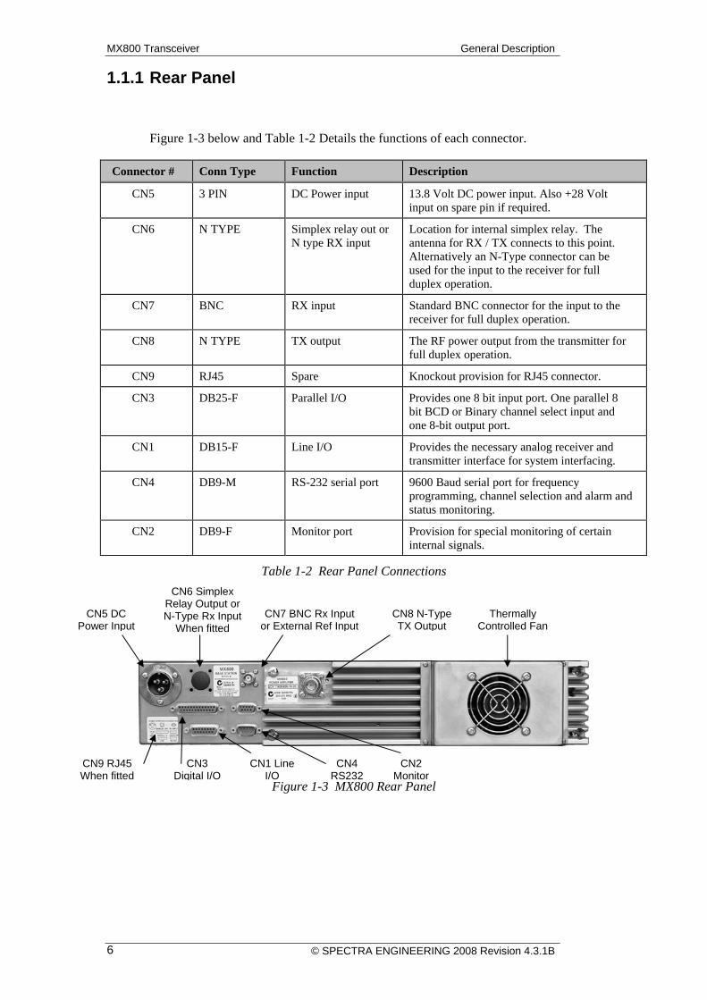
1.1.1 Rear Panel
Figure 1-3 below and Table 1-2 Details the functions of each connector.
Connector # Conn Type Function Description
CN5 3 PIN DC Power input 13.8 Volt DC power input. Also +28 Volt input on spare pin if required.
CN6 N TYPE Simplex relay out or N type RX input
Location for internal simplex relay. The antenna for RX / TX connects to this point. Alternatively an N-Type connector can be used for the input to the receiver for full duplex operation.
CN7 BNC RX input Standard BNC connector for the input to the receiver for full duplex operation.
CN8 N TYPE TX output The RF power output from the transmitter for full duplex operation.
CN9 RJ45 Spare Knockout provision for RJ45 connector.
CN3 DB25-F Parallel I/O Provides one 8 bit input port. One parallel 8 bit BCD or Binary channel select input and one 8-bit output port.
CN1 DB15-F Line I/O Provides the necessary analog receiver and transmitter interface for system interfacing.
CN4 DB9-M RS-232 serial port 9600 Baud serial port for frequency programming, channel selection and alarm and status monitoring.
CN2 DB9-F Monitor port Provision for special monitoring of certain internal signals.
Table 1-2 Rear Panel Connections
Figure 1-3 MX800 Rear Panel
Thermally Controlled Fan
CN8 N-Type TX Output
CN7 BNC Rx Input or External Ref Input
CN6 Simplex Relay Output or N-Type Rx Input
When fitted CN5 DC wer InPo put
CN2 Monitor
CN4 RS232
CN1 Line I/O
CN3 Digital I/O
CN9 RJ45 When fitted

Technical Manual General Description
1.1.2 Side Panel
The MX800 side view is illustrated in Figure 1-4 below. Two mounting holes in each side make provision for fitting a slider rail bracket.
les in each side make provision for fitting a slider rail bracket.
Figure 1-4 MX800 Side Panel Figure 1-4 MX800 Side Panel
Mounting Holes for Slide Rails
Sideways Airflow Permits MX800s to be Stacked in a Rack
1.2 Module Functional Description 1.2 Module Functional Description
1.2.1 Exciter Module 1.2.1 Exciter Module
The Exciter module generates the low level, on frequency, RF transmitter signal that is later amplified to nominal output power level by the Power Amplifier module. The exciter consists of a Voltage Controlled Oscillator (VCO) and associated main RF board, which, in conjunction with the reference oscillator and the PLL circuitry, forms a two-point modulation programmable frequency synthesiser. Frequency programming data is received from the Micro Controller via a 3 wire serial data bus.
The Exciter module generates the low level, on frequency, RF transmitter signal that is later amplified to nominal output power level by the Power Amplifier module. The exciter consists of a Voltage Controlled Oscillator (VCO) and associated main RF board, which, in conjunction with the reference oscillator and the PLL circuitry, forms a two-point modulation programmable frequency synthesiser. Frequency programming data is received from the Micro Controller via a 3 wire serial data bus.
The exciter module features a modulation bandwidth from DC with an ultra wide RF bandwidth of 20MHz to 1000MHz at an average RF output power of 300mW. To change from one band to another, all that is required is to change the plug in VCO board and reprogram the radio. No other manual adjustment or change is required.
The exciter module features a modulation bandwidth from DC with an ultra wide RF bandwidth of 20MHz to 1000MHz at an average RF output power of 300mW. To change from one band to another, all that is required is to change the plug in VCO board and reprogram the radio. No other manual adjustment or change is required.
Should a high stability reference be required, the exciter can be fitted with a connector for an external reference oscillator input. Should a high stability reference be required, the exciter can be fitted with a connector for an external reference oscillator input.
The fractional N synthesiser provides ultra low spurii while still maintaining fast lock times even at 6.25 kHz step size. The fractional N synthesiser provides ultra low spurii while still maintaining fast lock times even at 6.25 kHz step size.
An optional built in turn around mixer (TRM) provides advanced diagnostics such as receiver sensitivity tests. An optional built in turn around mixer (TRM) provides advanced diagnostics such as receiver sensitivity tests.
© SPECTRA ENGINEERING 2008 Revision 4.3.1B 7
MX800 Transceiver General Description
1.2.2 Receiver Module
The receiver module accepts the low level RF input signal and amplifies, filters and conditions the signal prior to detecting the wanted audio component. The Receiver module features the same advanced synthesiser and wide bandwidth as the exciter. Only the front-end Bandpass filter and VCO need to be changed in order to support different frequency bands, resulting in significant flexibility and end-user cost savings. The purpose built front end Bandpass filter has a wide no-adjust bandwidth equal to the band allocation (refer to section 7.4 for details of the band allocations).
The receiver has high sensitivity while maintaining excellent Intermodulation immunity and adjacent channel rejection. A dual first IF filter provides excellent rejection to common known spurious responses. High blocking of over 100dB typical ensures that strong interfering signals do not desensitise the receiver when receiving weak signals.
1.2.3 Power Amplifier Module
RF from the Exciter passes via a coaxial cable to the input of the PA Module and is first attenuated by a 50 ohm pad, which is used to provide a good 50 ohm source impedance for the first LDMOS driver amplifier. The RF is amplified to around 5 Watts at the driver output, and is band dependant. Note: this point does not have 50 ohm impedance and the drive power cannot be measured directly with a 50 ohm Wattmeter. The signal from the driver is then matched by a broadband network to drive the low input impedance associated with the final transmit LDMOS power amplifier transistor. The transistor's low Drain impedance is then also matched back to 50 ohms by a broadband matching network covering a very wide bandwidth. Prior to transmission, a low loss 13 element elliptical low pass filter, filters out the unwanted harmonics to less than –90 dBc.
A dual directional coupler consists of coupled microstrip transmission lines fabricated on the PCB artwork. The sampled RF energy is rectified to provide a proportional DC voltage output.
The PTT signal enables the amplifier circuit by providing bias to the transistors. A thermistor TS1, physically located on the PA heatsink monitors the heatsink’s temperature and is monitored by the Micro Controller.
The PA is very compact and efficient for high reliability and low cost. The heatsink has minimal temperature rise even under continuous operation, ensuring the best MTBF obtainable for a practical design.
© SPECTRA ENGINEERING 2008 Revision 4.3.1B 8

Technical Manual General Description
1.2.4 Micro Controller Board
The Micro Controller Board is physically located behind the rear panel connectors and all signal connections (apart from the RF connections) external to the transceiver are made via the controller card. User settable jumpers and DIP switches are located on the card as are level adjustment potentiometers.
The Micro Controller controls the operation of the RF modules and acts as the interface between the user connections, indicators and the RF modules. It processes transmit and received audio to and from the Exciter and Receiver modules as well as providing the digital I/O functions of the transceiver.
The circuit board has an onboard EEROM in which is stored all of the user channel related data such as frequencies, CTCSS tones etc. A serial port at the rear (or optionally the front) of the MX800 provides access to the Controller card and in conjunction with the Spectra Engineering "MXTOOLS" programming utility allows the user to create and change this channel related information.
Special functions capable of being carried out by this card include non-predictive full duplex CTCSS encoding/decoding, DCS encoding/decoding as well as FFSK and 4-level FSK modems. Digipots under the control of the processor ensure that user set up levels for TX deviation and power levels are correctly set for each channel.
© SPECTRA ENGINEERING 2008 Revision 4.3.1B 9

MX800 Transceiver General Description
This page left blank intentionally.
© SPECTRA ENGINEERING 2008 Revision 4.3.1B 10

Technical Manual
2. Installation and Operation 2.1 Installation
MX800 series radios are securely packed for transport with special moulded packers within a pasteboard container. Before unpacking the MX800 radio, please inspect the packaging for signs of damage and report any damage to your MX800 distributor.
Upon unpacking of the MX800 radio, please ensure that all items shipped were received, report any missing items to your MX800 distributor.
All ports on the rear of the radio should be carefully examined to ensure that packaging has not become wedged inside them. It is very important to examine the fan as operation of the radio will be affected if any packaging or shipping damage causes the fan to stop working.
If you intend to install the radio in an equipment rack consult the supplier’s instructions for your system. Spectra Engineering recommends that the radio be secured into the rack system using four screws through the mounting holes in the front panel near the handles. If the radio is to be used in a stand-alone configuration, ensure that it is in a secure, dry location with sufficient air space around it to allow for adequate ventilation.
It is recommended that the chassis is earthed to the equipment rack. A grounding screw terminal is provided on the left side of the main chassis for connection to the site ground point (Protective Earth). The wire is terminated with a closed loop ring terminal (eyelet) connector which is fixed to the earthing screw with a lock washer to stop them working loose. It is important that the earth wire connector is located at bottom, closest to the chassis.
The earthing conductor should be connected to the best possible earth, such as an earthed mounting plate or an earth rod. Remember that the earthing conductor must be as short as possible and lowest resistance typ. <0.1ohms.
It is recommended to protect the Base Station from lightning, by using a lightning arrestor. There are many publications covering antennas and their installation. Consult with your local dealer for more information and recommendations.
Equipment connection details are located in Appendix 7.1. The MX800 will draw approximately 10A (band dependent) on transmit and the gauge of the DC cable fitted to the 12V supply connector should be adequate to ensure less than 0.5V volt drop at this current. To maintain compliance with R&TTE (CE) approval the DC cable length should not exceed 3 metres.
NOTE: The MX800 contains No reverse polarity protection. Be sure both the positive (red) and negative (black) terminals are correctly connected and an inline 15Amp fuse is fitted on the Positive wire. See example in picture below (Not include). Fuse Link15Amp Fuse Inline Fuse
Holder
© SPECTRA ENGINEERING 2008 Revision 4.3.1B 11

MX800 Transceiver Installation & Operation
© SPECTRA ENGINEERING 2008 Revision 4.3.1B 12
2.2 Screw Head Types Modern screws employ a wide variety of drive designs, each requiring a different kind of tools to drive in or extract them. Spectra Engineering has chosen the Pozidriv ® screw head and screwdriver as it preferred screw type on all of its products, sizes 1 & 2. This is because the Pozidriv system is the choice for high volume assembly operations. It provides self-centring system and excellent driving control with less operator fatigue.
It is similar to the classic Phillips cross-head. The differences lie in the way that the heads are machined. The Phillips head has 4 simple slots cut out of it, whereas in the case of the Pozidriv each slot is the result of two machining processes at right angles. The result of this is that the arms of the cross are parallel sided in the case of Pozidriv, and tapered in the case of Phillips. The Pozidriv has four additional points of contact, and does not have the rounded corners that the Phillips screw drive has.
Phillips screwdrivers will usually work in Pozidriv screws, but Phillips screwdrivers are likely to slip or tear out the screw head when used in Pozidriv screws. It is important that you use the correct type and size screwdriver to avoid damaging the screw head.
Exrta contact pointsFigure 1-1 Top view of screw heads
Pozidriv Philliips
Parallel sides Tapered sides
Figure 1-2 Side View of screw Heads
Exrta contact ridges
Parrallel driving flute
Tapered driving flute
Figure 1-3 Screw driver Tip View
Used on All Spectra products
Don’t used this type on Spectra products
Pozidriv Phillips
Technical Manual Installation & Operation
2.3 Operation The MX800 can operate in local control mode via the front panel controls, stand alone repeater mode, or may be remotely controlled through the line port. Setting up the MX800 to operate in the wanted mode is straightforward and involves four main steps.
1. Using the MX800 programming utility 'MXTOOLS' to set the software configurable parameters.
2. Setting the hardware jumpers on the Micro Controller for the required options.
3. Adjusting the levels where necessary.
4. Making the necessary electrical connections to the radio and your system.
Note that generally if the requirements have been fully specified at time of purchase steps 1 to 3 will already have been done at the factory. In the following sections the hardware aspects of the set up procedure are described.
2.3.1 MXTOOLS Utility
MXTOOLS is a programming utility used to program channel data, configure and perform remote diagnostics on the MX800. It runs on a PC compatible computer and the MXTOOLS Inbuilt help menus cover use of the program.
2.3.1.1 MX800 Networking
See New Option T31 & T34 also.
At sites where more than one MX800 is located it is possible to "bus" the RS232 lines to allow up to 16 MX800s at one site to be addressed on a single RS232 port. Hardware facilities provided on the MX800 Micro controller card provide isolation between transmit ports. When MX800s are bussed in this way JMP24 in each radio must be set so that
1. At least one radio and no more than four are set as masters.
2. All other radios are set as slaves.
Refer to Table 2-1, in section 2.3.2.1 for details.
In addition to this, each radio must be assigned a unique address. This address is assigned as a binary code through CN3. Four address lines are available on input port A where bit 4 is the LSB and bit 7 is the MSB. These lines should be pulled high or low depending upon the setting of JMP19. Default is active low so that GND = Logic 1, Refer section 2.2.2.5.
The RS232 cable should be made up such that all MX800 transmit ports (TXD) are common and connected to the PC receive port (RXD) and all MX800 receive ports (RXD) are common and connected to the PC transmit port (TXD).
© SPECTRA ENGINEERING 2008 Revision 4.3.1B 13

MX800 Transceiver Installation & Operation
© SPECTRA ENGINEERING 2008 Revision 4.3.1B 14
MXTOOLS automatically polls the bussed radios to determine which addresses are active when the "Use Network" button is selected in the initial connect screen (MXTOOLS version 2.8.1 or later).
Refer application note AN-MX800-002 for more details on networking, available from www.spectraeng.com.au web site.
2.3.2 Setting to Work
The following sections describe the steps necessary to set the MX800 to operate as required.
2.3.2.1 Setting Micro Controller Jumpers
The micro controller layout is contained in the drawing section and the position of the jumpers and DIP switches (highlighted) are shown below. The jumpers and switches are used for setting the general configuration of the audio processing for both the TX and RX paths as well as various miscellaneous functions.
Table 2-1 below summarises the functions of the jumpers.
JMP Function / Description Default Selection
Default Position
JMP 1 Selects either default RUN or EMULATE mode for the micro processor.
Run 2-3
JMP 2 Enables the WATCHDOG auto reset function in the microprocessor.
Enabled 1-2
JMP 3 Enables or disables the PRE-EMPHASIS for the TX audio.
Enabled 1-2
JMP 4 Enables or disables the COMPRESSOR for the TX audio.
Enabled 1-2
JMP 5 Enables or disables the HIGH PASS FILTER for the RX audio.
Enabled 2-3
JMP 6 Enables or disables the LOW PASS FILTER for the RX audio.
Enabled 2-3
JMP 7 Enables or disables the DE-EMPHASIS processing for the RX audio.
Enabled 2-3
JMP 8 Enables a direct connection to the TX modulator. Select either Wide Band or Wide Band filtered and limited or nil.
DC-FM 1-2
JMP 9 TX VF Loopback control. Trunking LIFUISEN function. The function polarity or nil can be selected.
Active low 1-2

Technical Manual Installation & Operation
JMP 10 Controls the direction of the RS-232 TX and RX data.
Swap 2-3
JMP 11 Controls the direction of the RS-232 TX and RX data.
Swap 2-3
JMP 12 Trunking RX Talk function. Disables RX VF to line and TTR VF. The function polarity or nil can be selected.
Active low 1-2
JMP 13 Enables or disables the HIGH PASS FILTER for the TX audio.
Enabled 1-2
JMP 14 Repeater enable. Trunking LIFULOCEN function. The function polarity or nil can be selected. Note that this control is in parallel with DIP S/W 2/4
Active low 1-2
JMP15 Selects the connection for the common pin on the digital I/O connector to either ETH or + 5 volts.
ETH 2-3
JMP16 Enables or disables the Low frequency HPF used for the Repeater VF routing.
Enabled 1-2
JMP17 Selects the Mute / Squelch output polarity to either normally high or low.
Active low 1-2
JMP 18 Trunking TX Talk function. Disables TX VF to line and TTR VF. The function polarity or nil can be selected.
Active low 1-2
JMP 19
Selects either internal pull up to 5V or internal pull down to ETH for digital input on D25 connector.
Pull up
2-3
JMP 22 Microphone gain. Fit this jumper to increase Mic gain 33dB
Low gain Not fitted
JMP 23 Enable tone to speaker. Fit this jumper to enable tone
Disabled Not fitted
JMP 24 RS232 port termination. This jumper allows an internal termination to be selected or not for bussed RS232 connections. Up to 16 units may be bussed. All bussed bases are ‘listeners’ on the modem RS232 TX port. All bussed bases have their RS232 TX ports diode to the modem Rx port. Normal: Non-bussed mode. No resistor fitted. D10 out of circuit. Master: Bussed mode.
Normal 1-2 1-2 2-3
© SPECTRA ENGINEERING 2008 Revision 4.3.1B 15

MX800 Transceiver Installation & Operation
4K7 resistor across D10. Configure at least one and no more than four MX800 in this mode when multiple units connected. Slave: Bussed mode. D10 fitted, no resistor. Configure balance of bussed units in this mode.
3-4
JMP 25 Mute defeat enable. Mute defeat cannot be used if RX TALK line is required. To use mute defeat remove JMP12 and fit JMP 25. The control signal polarity can be inverted by changing the position of JMP25. Active low control: JMP25 2-3 Active high control: JMP25 1-2
Disabled Not fitted
JMP 26 CTCSS output / TX VF Loopback control
TX VF Loopback
2-3
JMP 27 CTCSS input / WB DC-FM input WB DC-FM input
2-3
Table 2-1 Micro Controller Jumpers
When the MX800 option card is not fitted there is no connection made to SKK (Aux 2 connector) on the micro controller. Links should be placed across SKK1-2 (Discriminator audio), SKK11-12 (TX supply) and SKK13-14 (RX supply). These links are normally fitted in production.
© SPECTRA ENGINEERING 2008 Revision 4.3.1B 16

Technical Manual Installation & Operation
2.3.2.2 Select Operating Mode
The MX800 can operate in a number of different modes. The primary alternatives are full duplex, which is the default mode, repeater and simplex. Using MXTOOLS the operating mode is programmed for each channel. When a channel is selected in operation the MX800 adopts the mode programmed for that channel.
The operating mode programmed in the software can be modified by the settings of DIP switch 2. The functions of this switch are detailed in Table 2-2 below.
SW 2 Function Description Def Select
1 PTT Delay Enables 50mS delay of PTT for use with simplex function.
OFF
2 Simplex Enable Enables simplex function* ON
3 TX Timer Sets programmable TX time out timer on
ON
4 Repeater Enable Enables repeater function* ON
5 TX VCO on continuously Switches TX VCO on continuously
OFF
6 Scan on Selects the receiver to enable the scanning of programmed scan channels
OFF
Table 2-2 DIP Switch 2 Settings
Note The Repeater Enable functions as follows: If the switch is ON and the channel is programmed as a repeater channel (using MXTOOLS) the MX800 will act as a repeater. If the switch is OFF the MX800 will remain in full duplex mode even if the channel is programmed as a repeater. The Simplex Enable operates in a similar way. In the case of the Repeater Enable function, the Repeater Enable on Pin 8 of the DB15 Line connector is effectively in parallel with SW2/4. If SW2/4 is OFF the function may be controlled through this external line. JMP 14 selects the control polarity in that case.
© SPECTRA ENGINEERING 2008 Revision 4.3.1B 17

MX800 Transceiver Installation & Operation
2.3.2.3 Select Operating Channel
The MX800 has a channel capacity of 255. The RF and CTCSS frequencies for each channel are programmed using MXTOOLS Channel Information screen. There are four ways of selecting the operating channel.
1. DIP Switch 8-way. DIP switch SW1 provides a binary channel selection facility. When a switch is ON it is read as a logical 1. When all switches are off the software channel select mode is enabled.
2. Rear channel select port. Digital input port B provides an 8 way Binary or BCD channel select input. Binary or BCD coding is selected using MXTOOLS. If Binary is selected 255 channels are accessible. If BCD is selected 99 channels are accessible.
3. Software channel select. If DIP switch SW1is set to 0 then it is possible to send a software command to the radio to select the channel.
4. Front panel Push-wheel switches. If this option is fitted the rear channel select port is internally wired to the Push-wheel switches however the rear channel select function is still in parallel with the Push-wheel. The rear select method should not be used in this case. There are 100 channels selectable from the front panel. The same rules apply to this channel select method as apply to the rear port described below. BCD Coding is selected using MXTOOLS.
The following rules apply. (The assumptions of logic levels are base on factory default setup. The Active state is Low)
DIP1 switches have priority over channel change. If any of DIP1 switches are set to ON (logic low) the rear inputs and the software Channel command will be ignored.
If DIP1 switches are set to OFF (logic high) then both the software commands and the rear input port would select the channel. In this case the most recent event will take priority. For example, if the rear input port is set to CH10 and a software command arrives to send it to CH15, the radio will go to CH15. If the rear input port is now changed to CH11 the radio will switch to CH11.
If DIP switches are set to OFF and the radio is powered up, the channel selected on the rear port will be adopted.
If DIP1 switches and the rear port are both set to OFF (logic High), on power up, the radio will adopt the last software channel selected. This may be the software channel set at the factory if the user has not used the software channel select feature before.
2.3.2.4 Configure Alarms/M Lead
The MX800 has 3 open collector outputs. Two of these are assigned as alarm outputs and one (output 1) may be configured as either an alarm output or an M Lead output. If the output one is configured as an M Lead, this line is active when mute is open and CTCSS/DCS is decoded. These outputs are assigned in the Configuration screen of MXTOOLS.
© SPECTRA ENGINEERING 2008 Revision 4.3.1B 18

Technical Manual Installation & Operation
2.3.2.5 Configure Digital I/O
The MX800 has 16 digital inputs and 8 general-purpose outputs. The inputs are +5V CMOS logic compatible and are buffered by a 10K resistor in series with each input. JMP19 on the Micro-Controller selects whether these inputs are internally pulled up or internally pulled low. The active state of the input is set up through MXTOOLS. Of the 16 inputs the 8 input port B inputs are allocated to the Channel Select function. Two of the input port A inputs (bit 0 and bit 1) are allocated to a power control function (see Table 2-3 below), two (bit 2 RX and bit 3 TX) are allocated to CTCSS control and the other 4 are allocated as address bits for the MX800 network mode (software V2.8.1 and higher).
Bit 1 Bit 0 RF O/P Power
0 0 100%
0 1 50%
1 0 20%
1 1 10%
Table 2-3 Power Control Function Settings
An auxiliary voltage (either +5V or GND dependant upon the setting of JMP15) is available on CN3 pin one for wiring convenience.
The 8 general-purpose outputs are +5V CMOS logic compatible and are buffered by a series 1K resistors.
2.3.3 Adjustments
There are two categories of adjustable parameters in the MX800. Those that are controlled by conventional potentiometers, which may be manually adjusted, and those controlled by digital potentiometers, which are under the control of the Micro Controller. The latter category of items comprises TX power, TX VCO deviation, TX reference oscillator deviation and TX reference oscillator frequency. All of these are adjusted with the aid of MXTOOLS and all except TX power should only be adjusted as a part of a full TX VF path alignment procedure.
Following adjustment of a digipot controlled parameter the value must then be saved to the radio to make the change permanent.
Refer to section 5 ‘Alignment and Testing’ for details.
© SPECTRA ENGINEERING 2008 Revision 4.3.1B 19

MX800 Transceiver Installation & Operation
This page left blank intentionally.
© SPECTRA ENGINEERING 2008 Revision 4.3.1B 20

Technical Manual
3. Options 3.1 T01 Programmable Channel Spacing
3.1.1 Description
The MX800 receiver is available in five different channel spacing options. For applications in systems that require both 12.5 kHz and 25 kHz channel spacing option T01 allows channels to be programmed for either bandwidth. Switchable IF filters in the receiver and automatic 12.5 kHz/25kHz gain compensation in the audio paths make the change in bandwidth transparent to the user.
This option has become Spectra’s standard build, therefore it is not necessary to specify this option at order placement. Once the switchable IF bandwidth receiver is fitted, the programmable channel spacing option must be selected on the MXTOOLS Configuration screen (Hardware Settings tab) and each channel is programmed as either 12.5 kHz/25kHz via the Channel Edit screen.
Figure 3-1 MX800 T01 Option, Programable bandwidth fitted to RX module.
3.1.2 Installation
This option is factory fitted.
© SPECTRA ENGINEERING 2008 Revision 4.3.1B 21
MX800 Transceiver Options
3.2 T02 Programmable CTCSS encoder/decoder
3.2.1 Description
Provision is made in the MX800 to fit a CTCSS encoder/decoder. The decoder is non-predictive and any valid CTCSS tone can be decoded. Any standard TX CTCSS tone may be associated with the programmed decode tone through the Channel Edit screen in MXTOOLS. Multiple CTCSS tones are programmable for any channel providing "Community Repeater" functionality.
This option may be fitted at order placement or retro fitted subsequently.
3.2.2 Installation
Components Required:
1. PART# C051 FX805 or MX805AP IC. Qty-1
Method:
1. Remove the cover to the MX800 radio.
2. Locate the socket for IC25 and install the MX805AP IC into this socket ensuring correct IC pin orientation.
MX800 Controller Setup:
1. The RF channels that are required to be CTCSS controlled should be programmed with the required CTCSS Subtone in the TX and/or RX channel fields.
MX800 Testing:
1. The Option T02 will require a ‘Peak Deviation and Modulation Balance Alignment’ as per Section 5 of the Technical manual. This alignment is to be performed without the CTCSS frequencies programmed into the alignment channel, as the subtone levels will give a false indication of the peak deviation levels.
© SPECTRA ENGINEERING 2008 Revision 4.3.1B 22

Technical Manual Options
3.3 T03 Programmable DCS/CTCSS encoder/decoder
3.3.1 Description
Provision is made in the MX800 to fit a full duplex DCS encoder/decoder. There are 83 digital codes available. Any standard DCS code or CTCSS tone may be assigned to any of the transmit or receive channels through the Channel screen in MXTOOLS. Multiple CTCSS tones are programmable for any channel providing "Community Repeater" functionality.
The DCS encoding function provides continuous, repetitive digital word modulation to the transmitter. The decode function controls receiver muting to eliminate all calls that are not coded with the assigned DCS code.
This option may be fitted at order placement or retro fitted subsequently. The DCS PCB assembly is fitted in place of IC25 (MX805AP). Once the DCS option is fitted the "DCS option fitted" check box is ticked in the MXTOOLS Configuration screen and the encode and decode codes are programmed through the Channel Edit screen.
Figure 3-2MX800 DCS Option T03
Refer circuit diagram CS001-4
3.3.2 Installation
Components Required:
1. DCS daughter board, complete with MX805AP IC’s. Qty-1
2. 3x8mm standoff post. Qty-1
Method:
1. Remove the cover to the MX800 radio.
2. Locate the socket for IC25, if necessary remove the IC from the socket.
3. Remove the 3x5mm screw that is located on the left hand edge and toward the front of the Motherboard from IC25 socket. Do not discard this screw.
4. Install the 3x8mm standoff post into the motherboard-mounting hole. Do not over-tighten this standoff.
© SPECTRA ENGINEERING 2008 Revision 4.3.1B 23

MX800 Transceiver Options
5. Install the DCS daughter board into the socket for IC25 ensuring that the daughter board has correct orientation with respect to pin numbering.
6. Install the 3x5mm screw (removed from step3) to secure the DCS daughter board.
MX800 Controller Setup:
1. The DCS option is activated in the MXTOOLS ‘Configuration’ heading, within the ‘Hardware’ folder with ‘DCS Option Installed’ selected.
2. The RF channels that are required to be DCS controlled should be programmed with the required DCS code in the TX and/or RX channel fields.
MX800 Testing:
1. If the MX800 had a CTCSS Option previously fitted, test the radio for correct operation of the DCS Option in both the Transmit and Receive modes.
2. If the Option T03 is not replacing a CTCSS Option then a ‘Peak Deviation and Modulation Balance Alignment’ as per Section 5.1.9 of the Technical manual will be necessary. This alignment is to be performed without the CTCSS/DCS frequencies programmed into the alignment channel, as the subtone levels will give a false indication of the peak deviation levels.
© SPECTRA ENGINEERING 2008 Revision 4.3.1B 24

Technical Manual Options
3.4 T05 Balanced and Isolated VF plus E&M
3.4.1 Description
Standard VF connections to line are 600ohm 4-wire unbalanced. Option T05 may be fitted if transformer balanced and isolated VF inputs and outputs are required. A transformer PCB is fitted internally at the rear of the MX800. This PCB has a RJ45 connector (CN9), which protrudes through the rear panel when this option is fitted, and the balanced VF outputs are made available via this connector.
Note that theses connections are essentially in parallel with the standard VF connections on CN1. The VF lines on CN1 are still connected when option T05 is fitted and care should be taken that the TX VF line is not doubly terminated or that two VF sources are not presented to the transmitter.
Note Jumpers referred to in the table below are those on this option PCB.
The E lead is opto isolated and may be asserted by applying a DC voltage between 5V and 48V with any polarity between CN9 Pins 7&8 (JMP1 in position 2-3, JMP2 removed). Provision is also made to internally source the activation voltage (+12V DC) in which case the E lead is asserted by grounding CN9 Pin8 (JMP1 in position 1-2, JMP2 fitted.)
The M lead is relay isolated and the common and normally open contacts are brought out via CN9. If the internal +12V DC is being used as the activation voltage for the E lead (JMP1 in position 1-2) then the normally closed contact is also available at CN9. The relay contacts are rated at 500mA.
Figure 3-3 MX800 Option T05 Balanced & Isolated VF I/O with E&M leads
25© SPECTRA ENGINEERING 2008 Revision 4.3.1B

MX800 Transceiver Options
Pin No Function
1 600ohm balanced RX VF leg a
2 600ohm balanced RX VF leg b
3 600ohm balanced TX VF leg a
4 600ohm balanced TX VF leg b
5 M Lead common
6 M Lead normally open
7 E Lead leg a/M lead normally closed
8 E Lead leg b
Table 3-1 CN9 Connections
The RJ45 pins are numbered as shown below.
1 .................. 8
Figure 3-4 CN9 RJ45 Pin-out Detail (View from Rear of MX800)
Refer circuit diagram CS018-1
3.4.2 Installation
Components Required:
1. Option board T05. Qty-1
2. 3x5mm machine screw. Qty-3
3. 10way Female-to-Female connector assy. Qty-1
4. 16way Female-to-Female connector assy. Qty-1
5. Rear connector layout label. Qty-1
Test Equipment Required:
1. Communications Test Set
2. MX800 Radio Interface Box
© SPECTRA ENGINEERING 2008 Revision 4.3.1B 26

Technical Manual Options
Method:
1. Remove the cover to the MX800 radio.
2. Remove the rear connector label from the back panel of the MX800.
3. Punch out the small indented rectangle on the rear LHS of the MX800.
4. Remove the connectors from the Motherboard headers SKE, SKF and SKH.
5. Carefully locate the T04 or T05 option board into position at the rear RHS of the radio with the RS232 cable lying underneath the option board.
6. Secure the option board with the qty3 3x5mm machine screws
7. Install the 10way Monitor cable to SK4 on the option board.
8. Install the 10way cable Assy to SK3 on the option board and to SKE on the Motherboard.
9. Install the 16way VF cable to SK2 on the option board.
10. Install the 16way cable Assy to SK1 on the option board and to SKH on the Motherboard.
11. Reconnect the 25way Digital Interface cable to SKF on the Motherboard.
12. Install the rear connector layout label onto the PA heatsink underneath the RF ‘N-type’ connector
MX800 Testing:
1. Connect a Communications Test Set via the RIB to the MX800 balanced audio RJ45 connector as per paragraph 3.4 of the MX800 Technical Manual.
2. Set the switches on the RIB to measure balanced audio and E&M.
3. Set the test set to measure Rx line level and adjust RV5 or RV5B for the level that is require if necessary.
4. Set the test set to measure TX modulation level and set the audio generator output level as per the required line level.
5. PTT the MX800 and measure the TX modulation depth. Adjust RV4 or RV4A for the modulation depth that is require if necessary.
6. To check the Rx isolated mute output, switch the RF level on the Comm.’s test set to ON. The Mute LED on the RIB should be ON. The LED should go OFF when the RF output from the test set is switched OFF.
7. Replace the MX800 cover.
© SPECTRA ENGINEERING 2008 Revision 4.3.1B 27

MX800 Transceiver Options
3.5 T06 Simplex Changeover Relay
3.5.1 Description
For simplex applications an internally mounted coaxial changeover relay can be provided. This mounts on the rear panel and the common port protrudes through the chassis providing the simplex antenna connection. The relay normally closed port is internally connected to the MX800 receiver and the normally open port is connected to the transmitter via the standard RX connector hole in the chassis (the RX connector is removed) using a special cable assembly. The relay also has control connections to the micro controller PCB.
Once the relay option is fitted the channels are programmed as simplex channels through the Channels Edit screen of MXTOOLS. Switches SW2/1 & SW2/2 on the micro controller are switched ON to delay the transmitter PTT (to allow the relay to changeover) and set the simplex operating mode respectively.
Figure 3-5 T06 Simplex Changeover Relay
© SPECTRA ENGINEERING 2008 Revision 4.3.1B 28

Technical Manual Options
3.5.2 Installation
Components Required:
1. Coaxial Relay Assy complete with Rx cable connected. Qty-1
2. RG58 cable Assy complete with ‘N’ Type connector fitted. Qty-1
3. 13mm hole grommet. Qty-1
4. 3x8mm pozi-drive screw. Qty-2
5. Rear Connector Label Qty-1
Test Equipment Required:
1. Communications Test Set
2. MX800 Radio Interface Box
Method:
1. Remove the cover to the MX800 radio.
2. Remove the existing Receiver coaxial feeder cable assy.
3. Install the 13mm grommet into the 13mm hole where the BNC Rx connector is normally located.
4. Place the RG58 cable Assy through the grommet so that the ‘N’ Type connector will mate with the ‘N’ Type female connector on the PA module.
5. Remove the 4x Phillips screws and connector cover from the TX side of the coax relay assy.
6. Solder the centre of the RG58 Cable Assy to the centre pin on the TX side of the coaxial relay. The outer sheath of the coax cable should be placed such that it sits equal with the outer edge of the relay body.
7. Place the connector cover over the TX cable on the relay and screw the cover in place. Take extreme care to not over-tighten the screws and prevent stripping of the threads in the relay body.
8. Install the relay Assy into the MX800 with the relay coil on the opposite side of the relay to the DC power connector. Secure with the 2 of 3x8mm screws provided.
9. Route the Rx coaxial cable to the Rx unit input RF connector.
10. Connect RG58 cable Assy to the PA output.
© SPECTRA ENGINEERING 2008 Revision 4.3.1B 29

MX800 Transceiver Options
11. Replace the rear connector label with the label supplied.
MX800 Controller Setup:
1. The MX800 RF channels that are required to be simplex should be programmed as ‘SIMPLEX’ within the channel edits screen of Mxtools and then downloaded to the MX800.
2. Switches SW2/1 and SW2/2 on the microcontroller board are switched ‘ON’ as per Section 3.6 of the MX800 Manual.
MX800 Testing:
1. Connect a Communications Test Set via the RIB to the MX800.
2. Set the switches on the RIB to Line Audio and E&M.
3. Set the test set to measure Rx line level and ensure that the Receiver is operating correctly.
4. Set the test set to measure TX modulation level and set the audio generator output level as per the required line level.
5. PTT the MX800 and measure the TX Power and modulation depth. Ensure that the coaxial relay operates correctly and that the full RF power is measured on the test set.
6. Operate the PTT in quick succession and ensure that the coaxial relay operates in unison with the PTT switch.
7. Replace the MX800 cover.
© SPECTRA ENGINEERING 2008 Revision 4.3.1B 30

Technical Manual Options
3.6 T08 VF Delay
3.6.1 Description
This option provides a 40mS delay to the received audio. When the option is fitted delayed audio is fed to the line and talkthrough paths but discriminator audio (output on CN1 Pin4) is undelayed.
This option is intended for two main applications. Firstly when the delay is fitted, the mute (squelch) "crash" characteristically heard when a mobile releases its PTT but the repeater tail continues, it is eliminated. Secondly systems (including trunking systems) which have mixed voice and data on a channel can delay the VF signal to line and air so that in the event that a data stream is detected (by the data controller) the VF to line and air can be disconnected for the duration of the data burst thus avoiding radio system user annoyance. Internal switches in the MX800 may be used to disconnect the audio under the control of the RX TALK line (CN1 Pin7) the sense of which may be inverted using JMP12 on the micro controller. This option provides quiet mute switching similar to CTCSS Reverse burst.
This option may be fitted at order placement or retro fitted subsequently. The Option PCB assembly is fitted above the Micro controller on four hex pillars. A 16-way ribbon connection is made from the Option PCB to SKK on the micro controller card. The links on the Option card are set as below. Once the delay option is fitted the "Delayed Audio Option" check box is ticked in the MXTOOLS Configuration screen (Hardware settings tab).
Note that this options PCB is also used for T09, CTCSS Suppression Upgrade Filter and T10, the Low Standby Current Mode and all three are independent and may be used separately or together. If the option PCB is ordered for one particular option it may or may not be populated for the other options.
Figure 3-6MX800 T08,T09,T10 Option board complete
© SPECTRA ENGINEERING 2008 Revision 4.3.1B 31

MX800 Transceiver Options
© SPECTRA ENGINEERING 2008 Revision 4.3.1B 32
JMP Function/Description Option Active Option Disabled
JMP 1 Low standby current mode switched exciter power
Out In
JMP 2 Low standby current mode switched receiver power
Out In
JMP 3 300Hz Elliptic filter 1-2 2-3
JMP 4 RX audio delay 2-3 1-2
Table 3-2 Option PCB Link Settings
Refer circuit diagram CS022-1B
3.6.2 Installation
Components Required:
1. Option board ‘MXOPT’ fitted for VF Delay option. Qty-1
2. 16way female-to-female IDC Cable Assy. Qty-1
3. 3x20mm Standoff posts. Qty-4
Test Equipment Required:
1. Communications Test Set
2. MX800 Radio Interface Box
Method:
1. Remove the cover to the MX800 radio.
2. Remove qty4 of the Motherboard securing screws as shown.
3. Install the qty 4 3x20mm standoff posts into the vacant screw positions.
4. Remove the Link jumpers off connector SKK.
Motherboard
3x5mm machine screws to be removed

Technical Manual Options
5. Install the Option PCB onto the 4 standoffs with the 16way connector closest to DIP2 on the Motherboard. Secure with the qty4 3x5mm machine screws previously removed.
6. Install the 16way-ribbon cable between connector SKK on the Motherboard and SKK on the Option board, taking note that the cable is correctly orientated.
7. Check that the option board jumpers are in the following positions;
1. JMP1 IN 2. JMP2 IN 3. JMP3 OFF 4. JMP4 ON
MX800 Controller Setup:
1. The VF Delay option is activated in the MXTOOLS ‘Configuration’ heading. Within the ‘Hardware’ folder select ‘Delayed Audio Option’.
2. Download the Configuration change to the MX800.
MX800 Testing:
1. Connect a Communications Test Set via the RIB to the MX800.
2. Set the switches on the RIB to Line Audio and E&M.
3. Set the test set to measure Rx line level and ensure that the Receiver is operating correctly.
4. Whilst listening to the RX audio output, switch the RF output on the Comm.'s test set on and off and note that there is NO distinctive ‘Click’ in the audio when the RF is switched OFF.
5. Replace the MX800 cover.
3.7 T09 300Hz Upgrade HPF Filter
3.7.1 Description
This option provides upgraded CTCSS tone suppression on the RX VF. When this option is fitted the standard 300Hz filter is removed from circuit by changing the position of JMP5 on the micro controller to position 1-2.
This option may be fitted at order placement or retro fitted subsequently. The Option PCB assembly is fitted above the Micro controller on four hex pillars. A 16-way ribbon connection is made from the Option PCB to SKK on the micro controller card. The links on the Option card are set as below. This option is purely a hardware change and no configuration is required using MXTOOLS.
© SPECTRA ENGINEERING 2008 Revision 4.3.1B 33

MX800 Transceiver Options
© SPECTRA ENGINEERING 2008 Revision 4.3.1B 34
Note that this options PCB is also used for T08, VF Delay and T10, the Low Standby Current Mode and all three are independent and may be used separately or together. If the option PCB is ordered for one particular option it may or may not be populated for the other options.
JMP Function/Description Option Active Option Disabled
JMP 1 Low standby current mode switched exciter power
Out In
JMP 2 Low standby current mode switched receiver power
Out In
JMP 3 300Hz Elliptic filter 1-2 2-3
JMP 4 RX audio delay 2-3 1-2
Table 3-3 Option PCB Link Settings
3.7.2 Installation
Components Required:
1. Option board ‘MXOPT’ fitted for 300Hz HPF Option. Qty-1
2. 16way female-to-female IDC Cable Assy. Qty-1
3. 3x20mm Standoff posts. Qty-4
Test Equipment Required:
1. Communications Test Set
2. MX800 Radio Interface Box
Method:
1. Remove the cover to the MX800 radio.
2. Remove qty4 of the Motherboard securing screws as shown.
3. Install the qty 4 3x20mm standoff posts into the vacant screw positions.
4. Remove the Link jumpers off connector SKK.
Motherboard
3x5mm machine screws to be removed

Technical Manual Options
5. Install the Option PCB onto the 4 standoffs with the 16way connector closest to DIP2 on the Motherboard. Secure with the qty4 3x5mm machine screws previously removed.
6. Install the 16way-ribbon cable between connector SKK on the Motherboard and SKK on the Option board, taking note that the cable is correctly orientated.
7. Check that the option board jumpers are in the following positions;
1. JMP1 IN 2. JMP2 IN 3. JMP3 ON 4. JMP4 OFF
MX800 Controller Setup:
Change the Motherboard jumper JMP5 to position 1-2 (OFF).
MX800 Testing:
Connect a Communications Test Set via the RIB to the MX800.
Set the switches on the RIB to Line Audio and E&M.
Using Mxtools program the appropriate RX CTCSS Tone required.
Set the Comm.’s test set to measure Rx line level and ensure that the Receiver is operating correctly and there is no CTCSS component on the Rx audio.
Replace the MX800 cover.
3.8 T10 Power Save Mode
3.10.1 Description
For solar powered sites and other power critical applications the MX800 is capable of a Power Save (Low Standby Current) Mode. This option can be implemented in three stages. Stage one implementation replaces the micro controller linear voltage regulators with switching regulators. Response times are unaffected. Stage two involves removing power from the exciter when the radio is in standby mode. In this case RX responses times are unaffected. In stage three the RX power is cycled on and off at a user selectable duty cycle. Essentially the choice of mode of operation involves a compromise between response time and average current consumption. Current consumption of 250mA is achievable with a typical response time in the order of 1sec.
© SPECTRA ENGINEERING 2008 Revision 4.3.1B 35

MX800 Transceiver Options
Condition Description Approx Average Current Drain mA
Standard Standard MX800 (TX VCO on continuously) 525
Standard Standard MX800 (TX VCO switched) 490
Stage 1a Standard MX800 (TX VCO on continuously) option board fitted
475
Stage 1b Standard MX800 (TX switched) option board fitted
440
Stage 2 TX exciter inc TX VCO powered down 370
Stage 3 RX 100% duty
TX exciter inc TX VCO powered down RX module power duty cycled
370
Stage 3 RX 50% duty
TX exciter inc TX VCO powered down RX module power duty cycled
255*
Stage 3 RX 25% duty
TX exciter inc TX VCO powered down RX module power duty cycled
198*
*Average current calculation is based on RX off current drain of 140mA and RX on current drain of 370mA.
Table 3-4 Current Consumption Details
This option may be fitted at order placement or retro fitted subsequently. The Option PCB assembly is fitted above the Micro controller on four hex pillars. A 16-way ribbon connection is made from the Option PCB to SKK on the micro controller card. The links on the Option card are set as below. Once the power save option is fitted the "Power Save Option Board Installed" and "Power Save Exciter Module" check boxes are ticked in the MXTOOLS Configuration screen (Hardware settings tab). In addition three timers need to be set. "Idle Time to Power Save" is entered in seconds and defines how long the radio will wait following the most recent activity before reverting to standby mode. "RX Module On Time" and "RX Module OFF Time" define the duty cycle of the receiver module.
Note that this options Printed Circuit Board is also used for T08, VF Delay and T09, CTCSS Suppression Upgrade Filter and all three are independent and may be used separately or together. If the option PCB is ordered for one particular option it may or may not be populated for the other options. If the option is being retrofitted the two main 5 Volt 78M05 regulators on the Microcontroller board must be removed and subsequently replaced if de-installing.
JMP Function/Description Option Active Option Disabled
JMP 1 Low standby current mode switched exciter power
Out In
JMP 2 Low standby current mode switched receiver power
Out In
JMP 3 300Hz Elliptic filter 1-2 2-3
JMP 4 RX audio delay 2-3 1-2
Table 3-5 Option PCB Link Settings
© SPECTRA ENGINEERING 2008 Revision 4.3.1B 36

Technical Manual Options
© SPECTRA ENGINEERING 2008 Revision 4.3.1B 37
Refer circuit diagram CS022-1
3.10.2 Installation
Components Required:
1. Option board ‘MXOPT’ fitted for Power Save Mode. Qty-1
2. 16way female-to-female IDC Cable Assy. Qty-1
3. 3x20mm Standoff posts. Qty-4
Test Equipment Required:
1. Communications Test Set
2. MX800 Radio Interface Box
Method:
1. Remove the cover to the MX800 radio.
2. Remove the Motherboard from the MX800 radio.
3. Remove IC’s 21 and 27 from the Motherboard.
4. Reinstall the Motherboard into the MX800 radio and using the qty 4 3x20mm standoff posts in the positions indicated below:
5. Remove the Link jumpers off connector SKK.
6. Install the Option Printed Circuit Board onto the 4 standoffs with the 16way connector closest to DIP2 on the Motherboard. Secure with the qty4 3x5mm machine screws previously removed.
7. Install the 16way-ribbon cable between connector SKK on the Motherboard and SKK on the Option board, taking note that the cable is correctly orientated.
8. Check that the option board jumpers are in the following positions;
1. JMP1 OUT
Motherboard
3x5mm machine screws to be removed

MX800 Transceiver Options
2. JMP2 OUT 3. JMP3 OFF (2-3) 4. JMP4 OFF (1-2)
MX800 Controller Setup:
1. The Power Save option is activated in the MXTOOLS ‘Configuration’ heading. Within the ‘Power Save Mode Settings’ folder select ‘Power Save Option Board Installed’.
2. Setup the power save mode settings as required.
3. Download the Configuration change to the MX800.
MX800 Testing:
1. Connect a Communications Test Set via the RIB to the MX800.
2. Set the switches on the RIB to Line Audio and E&M.
3. Check that all the Transmit parameters (i.e. TX power, modulation, freq. error) are correct. Correct any anomalies where necessary.
4. Set the test set to measure Rx parameters and ensure that the Receiver is operating correctly.
5. Replace the MX800 cover.
3.9 T11 Combined Options This option combines the functions and features of T08, and T10
3.10 T12 External Reference Oscillator Input Please also see section 3.19 and 3.13
3.12.1 Description
The MX800 receiver and transmitter modules have separate reference oscillators. In normal operation to achieve a low frequency transmitter modulator frequency response to DC, the MX800 normally uses a two-point modulation method. For two-point modulation, the TX reference oscillator and the VCO are both modulated together and in phase. Option T12 provides for the TX reference frequency to be externally injected. An SMB connector is fitted to the exciter and an internal cable is provided from there to a chassis mount N Type connector into which the external reference frequency is injected. As two-point modulation is not possible with this configuration, the transmitter frequency response is only specified to 67Hz for this option.
The N Type connector will be required to be used for the RX I/P in which case the BNC becomes the external reference I/P.
© SPECTRA ENGINEERING 2008 Revision 4.3.1B 38

Technical Manual Options
A range of reference frequencies from 1MHz to 16MHz can be used with this option. With MXTOOLS, check your exact frequency can be programmed and accepted.
3.12.2 Installation
Components Required:
1. BNC to Right Angle SMB Coaxial Cable Assy. Qty-1
2. N-Type to Right Angle SMB Coaxial Cable Assy. Qty-1
3. SMB right angle PCB mounted connector. Qty-1
4. Rear connector layout label Qty-1
5. 3x8mm machine screws Qty-4
6. Rear Connector label Qty-1
Test Equipment Required:
1. Communications Test Set
2. MX800 Radio Interface Box
Method – MX800 Chassis:
1. Remove the cover to the MX800 radio.
2. Remove the ribbon cable from the Exciter module.
3. Remove the coaxial cable Assy from the Exciter module.
4. Remove the Exciter module from the chassis by unscrewing the 2 M4x35mm screws.
5. Remove the receiver coaxial cable Assy from the chassis – Do not discard the 2.5x5mm screws.
6. Remove the 16mm plug from the Simplex relay position.
7. Install the N-type coaxial cable Assy into the 16mm hole and secure with the 3x8mm machine screws. Route this cable to the receiver module and connect to the receiver-input connector.
8. Install the BNC-type coaxial cable Assy into the 13mm hole and secure with the qty4 2.5x5mm screws. Route this cable underneath the PA module to the location of the exciter External Reference input connector.
9. Re-install the exciter module (after it has been modified for this option) with the qty2 4x35mm machine screws.
10. Connect all the necessary connectors to the exciter module.
11. Replace the rear connector label with that supplied.
© SPECTRA ENGINEERING 2008 Revision 4.3.1B 39

MX800 Transceiver Options
Method – Exciter Module:
1. Remove the cover to the exciter module.
2. Remove the exciter Printed Circuit Board from the base unit.
3. Remove the following components from the exciter board:
• X1 - TCXO
• R30 & R31
• TR7
4. Install and solder the right angle SMB PCB mounted connector into the CN3 position on the exciter Printed Circuit Board.
5. Re-install the exciter Printed Circuit Board onto the base unit.
6. Re-install the cover to the exciter module.
MX800 Controller Setup
1. The TX external reference frequency that will be used is required to be programmed into the radio via MXTOOLS. This can be achieved in the MXTOOLS ‘Configuration’ heading under the ‘Hardware’ folder, insert the required frequency into the ‘TX Reference Frequency’ box.
2. Download the Configuration change to the MX800.
MX800 Testing:
1. Connect a Communications Test Set via the RIB to the MX800.
2. Set the switches on the RIB to Line Audio and E&M.
3. Connect the External Reference source to the MX800 BNC connector.
4. Check that the exciter VCO is in ‘lock’.
5. Check that all the Transmit parameters (i.e. TX power, modulation, freq. error) are correct. Correct any anomalies where necessary.
6. Set the test set to measure Rx parameters and ensure that the Receiver is operating correctly.
7. Replace the MX800 cover.
© SPECTRA ENGINEERING 2008 Revision 4.3.1B 40

Technical Manual Options
© SPECTRA ENGINEERING 2008 Revision 4.3.1B 41
3.11 T13 Local Speaker, Mic Socket and Front Panel Mute
3.11.1 Description
For applications needing a user interface at the base station the MX800 is available with the Local Control option. The full implementation is described in section 1.1.1.2 this section describes the part fitted under option T13.
Figure 3-7 Front Panel with Speaker, Mic and Mute
Loudspeaker and Volume Control A 1 Watt loudspeaker is provided to monitor 'on air' received audio as well as transmit audio from line. Volume control is provided by means of a volume pot or a 3-position toggle switch adjacent to the loudspeaker. This switch is biased in the centre position. To raise or lower the volume the switch is momentarily moved up or down respectively. For each switch closure the volume is incremented or decremented a fixed amount. The speaker has a link selectable connection to a tone output from the micro controller. This may be used in conjunction with the appropriate software configuration to generate an alert tone to the user.
Microphone Socket An RJ45 socket is provided for connection of a microphone. This socket is wired compatibly with the Motorola GM300 microphone.
Mute / Squelch Adjustment Provision is made to optionally locate the squelch control potentiometer behind the front panel. A screwdriver hole is provided in the front panel to access this adjustment.
RS232 Port Line I/P Adjust HoleSpeake
Push-wheelChannel Change
r
VolumeControl
RJ45Microphone
Socket
SquelchAdjust Hole
Line O/PAdjust Hole

MX800 Transceiver Options
Pin No Function Comment
8 PB1 5V CMOS input
7 PB2 5V CMOS input
6 Hook/monitor For quiet base
5 Mic ETH
4 Mic VF in. High or low level Set JMP22 IN for low gain dynamic Mic
3 Mic PTT. Pulled to +5V via 10K
2 +5 volts out Current limited via 220R
1 Low level muted RX VF Fixed level out.
Table 3-6 MX800 Mic Socket Pinout
The RJ45 pins are numbered as shown in Figure 3-4 below.
1 .................. 8
Figure 3-8 RJ45 socket viewed from front of MX800
Refer circuit diagram CS001-6 sheet 6 of 6
3.11.2 Installation
CAUTION: COMPONENTS USED ARE STATIC DAMAGE SENSITIVE!
Components Required:
1. Front Panel and matching Handles. Qty-1
2. Loudspeaker. Qty-1
3. MCP6002D Integrated Circuit. Qty-3
4. TDA8551 Integrated Circuit. Qty-1
5. RJ45 PCB mounted Microphone socket. Qty-1
6. 16mm Volume Pot or SPDT momentary Volume switch. Qty-1
7. 100kohm 10turn PCB mounted squelch potentiometer. Qty-1
8. 100kohm SMD potentiometer. Qty-1
9. Jumper link connector. Qty-1
© SPECTRA ENGINEERING 2008 Revision 4.3.1B 42

Technical Manual Options
Test Equipment Required:
1. Communications Test Set
2. Jumper link
Installation Method – MX800 Chassis:
1. Remove the cover to the MX800 radio.
2. Remove the motherboard from the chassis.
3. Remove the Exciter and receiver modules from the chassis by unscrewing the 2 M4x35mm screws on each module.
4. Remove the front panel from the chassis by unscrewing the qty4 screws securing the handles to the front panel – Do not discard the screws.
5. Place the loudspeaker in the speaker indentation on the front of the chassis. The speaker wires should be in the upper most position.
6. Place the front panel on the front of the chassis to hold the speaker in position and secure the front panel with the matching handles and the previously removed screws. Ensure that the front panel holes are aligned with the corresponding chassis holes and fully tightened handle screws.
7. Re-install the exciter and receiver modules into the chassis.
8. Re-install the motherboard (after it has been modified for this option) into the chassis being careful to align the front panel hole positions with the corresponding motherboard components.
9. Re-connect all of the modules and chassis mounted connectors to the motherboard via their appropriate cable assembly’s.
Installation Method Motherboard:
1. Install the MCP6002 IC’s onto circuit board designations IC61, IC62 & IC64.
2. Install the TDA8551 IC onto circuit board designations IC60.
3. Remove the SMB potentiometer located on circuit board designation RV6 and re-install it onto board reference RV10.
4. Install the 100kohm SMB potentiometer onto circuit board designation RV11.
5. Install the 100kohm PCB potentiometer onto circuit board designation RV6B (Mute).
6. Install and solder the RJ45 connector into the SKL (MIC) position on the motherboard board.
7. Install and solder the 16mm Volume Pot (RV9) or SPDT switch into the SW1 (VOL) position on the motherboard board.
© SPECTRA ENGINEERING 2008 Revision 4.3.1B 43

MX800 Transceiver Options
8. Link the necessary links near RV9 as instructed on motherboard.
9. Install the jumper link to JMP25 (Tone to Speaker) on the motherboard.
MX800 Software Controller Setup: There is no specific Controller setup required. MX800 Testing – Speaker:
1. Connect a Communications Test Set (CTS) and the necessary I/O connection to the MX800.
2. Connect Dummy load to MX800 RF out put (CN8)
3. Connect the MX800 Rx input to the RF out (or Duplex out) of the CTS.
4. Set-up the CTS for operation with the audio generator set to 1kHz @ -10 dBm and the audiometer to show Audio input level.
5. Disconnect Speaker from SKM and Connect CTS Audio in to the speaker output connector SKM (SPKR).
6. Operate the volume control for maximum audio output, monitor this on the CTS and then adjust RV10 until the audio level is +5dBm. Reduce the audio level using the volume control and connect the MX800 speaker to SKM.
MX800 Testing – Microphone:
1. Connect a Communications Test Set (CTS) and the necessary MX800 I/O connection. Connect a Microphone cable to the Microphone socket of the MX800 so that you can inject into pins 4 (Mic Audio) & 5 (GND). You’ll also need to connect a switch or be able to short pins 3 & 5.
2. Set-up the CTS for duplex operation with the audio generator set to -20 dBm and the audiometer to show output line level. With Rx line (CN1 pin 15) audio connect to CTS audio input.
3. PTT the MX800 and adjust RV11 for –10dBm on the audio level meter.
4. Set the audio generator for –50dBm and install a jumper link onto JMP22 on the motherboard. The audio meter should read approx. –9dBm and reducing the audio generator level in 1dB increments the meter level should also reduce, increasing the level should cause the audio cct to limit the audio level to approx. –8dBm.
5. Remove the Link from JMP22 and increase the audio generator level to –10 dBm.
6. Set the test set to display TX modulation depth and measure the modulation level. The modulation level should be approximately equal to the nominal deviation level for the Transmitter. I.e. 3 kHz wide band and 1.5 kHz Narrow band.
7. Remove the Microphone cable from the MX800 MIC socket.
© SPECTRA ENGINEERING 2008 Revision 4.3.1B 44

Technical Manual Options
MX800 Testing – Rx Mute:
1. Connect a Communications Test Set (CTS) and the necessary MX800 I/O connection.
2. Set the test set to measure SINAD and reduce the RF generator until 8db SINAD is reached.
3. Adjust the front panel Mute control so that the RX just goes into the muted condition.
Testing in now complete.
3.12 T14 Local Channel Change
3.12.1 Description
For applications needing a user interface at the base station the MX800 is available with the Local Control option. The full implementation is described in section 1.1.1.2, this section describes the part fitted under option T14.
Channel Change Control Twin push wheel switches can be optionally fitted to the front panel to allow selection of the operating channel. When fitted this switch is wired to the channel select pins on SKF/E, the rear channel select port, and replaces the channel select function normally accessible on the rear digital I/O connector. 99 channels are selectable. Refer to section 2.2.2.3 for more details on alternative channel select methods.
3.12.2 Installation
Components Required:
1. Local Channel Change Switch and Cable Assembly. Qty-1
2. Front Panel and matching Handles. Qty-1
Test Equipment Required:
1. Communications Test Set
2. MX800 Radio Interface Box
© SPECTRA ENGINEERING 2008 Revision 4.3.1B 45

MX800 Transceiver Options
Method:
1. Remove the cover to the MX800 radio.
2. Remove the motherboard from the chassis.
3. Remove the Exciter and receiver modules from the chassis by unscrewing the 2 M4x35mm screws on each module.
4. Remove the existing front panel from the chassis by unscrewing the qty4 screws securing the handles to the front panel – Do not discard the screws.
5. Place the upgrade front panel on the front of the chassis and secure with the matching handles and the previously removed screws. Ensure that the front panel holes are aligned with the corresponding chassis holes and fully tightened handle screws.
6. Install the local channel change switches into the front panel hole and secure into position hot melt glue.
7. Route the switch Assy cable along the front of the chassis and to the rear of the motherboard standoff posts closest to the front of the chassis. Secure into position with a small piece of tape.
8. Re-install the exciter and receiver modules into the chassis.
9. Re-install the motherboard into the chassis being careful to align the front panel hole positions with the corresponding motherboard components.
10. Re-connect all of the modules and chassis mounted connectors/switches to the motherboard via their appropriate cable assembly’s.
MX800 Controller Setup:
1. The Local Channel Change option is activated in the MXTOOLS ‘Configuration’ heading, within the ‘Software’ folder with ‘Channel Select Input’ selection of ‘BCD’.
2. Download the configuration change to the MX800.
MX800 Testing:
1. Connect a Communications Test Set and the RIB to the MX800.
2. Set the switches on the RIB to Line Audio and Line E&M.
3. Set MXTOOLS into Diagnostics mode and ‘Start’ the diagnosis process.
4. Change the channel on the local channel switches and check that the channel selected on the BCD switch is in fact the channel that the Diagnostics screen indicates.
5. Reset the MX800 operating channel to the required position.
© SPECTRA ENGINEERING 2008 Revision 4.3.1B 46

Technical Manual Options
3.13 T16 1PPM Frequency Stability 12.5 kHz channels Frequency band K to X (320-950MHz) 25.0 kHz channels Frequency band R to X (805-950MHz)
This option provides for 1PPM frequency stability for narrowband MX800s in the K to X bands. This frequency stability is specified from –30° C to +60° C.. 1PPM stability can additionally be used on any frequency band above 66 MHz but the DC-FM transmitter modulation feature is not fully specified below 400 MHz. Typically, this results in only some minor drop of the low freq response or ability to set up the Transmitter modulation balance.
Also see section 3.19 and 3.10
3.14 U69 Extended Temperature Range Verification
The MX800 is optionally available in an extended operating temperature range version, extending the temperature range over –30° C to –10° C. Additional testing and operational verification is done in an environmental chamber at –30C for 24 Hours. An additional factory test report sheet is provided at his temperature. Frequency stability is specified at 2.5PPM for this option.
3.15 T19/26 Line Interface Board. The MX800 T19 / T26 option board provides the radio base station with utmost flexibility in system design and capabilities, with an extensive range of new features.
Please consult Spectra, for the availability of these features or software upgrades. Not all features are currently available.
♦ 2Wire (VF Hybrid) or 4Wire Selection, Balanced Audio, Dual E+M, ♦ VF Delay (To replace option T08)
Provides quiet mute switching similar to CTCSS Reverse burst. ♦ Base Station Variable Tone Voting ♦ Base Station Stepped Tone Voting ♦ Status Tone Encoding And Decoding (T19 only) ♦ Five Tone Encoded / Decoder (T19 only) ♦ DTMF Decoder ♦ Remote Control Capabilities ♦ Fast CTCSS Decoder ♦ VF Line compensation for SINAD Voters ♦ Real-time Clock
Due to ongoing development please refer to www.spectraeng.com.au for the latest information regarding this option. A technical manual is available for this option please contact [email protected] for a copy of this manual.
© SPECTRA ENGINEERING 2008 Revision 4.3.1B 47

MX800 Transceiver Options
3.16 T29 Balanced and Isolated VF plus E&M 3.16.1.1 Description
Option T29 provides the balanced and isolated VF I/O as well as isolated E (PTT) and M (Mute) leads, as per option T05. The option has been design to be compatible with Omitronics™ interface connections.
Note Jumpers referred to in the table below are those on this option PCB. The E lead is opto isolated and may be asserted by applying a DC voltage between 5V and 48V with any polarity between CN9 Pins 1&2 (JMP1 in position 2-3). Provision is also made to internally source the activation voltage (+12V DC) in which case the E lead is asserted by grounding CN9 Pin2 (JMP1 in position 1-2)
The M lead is relay isolated and the common and normally open contacts are brought out via CN9. If the internal +12V DC is being used as the activation voltage for the E lead (JMP3 in position 1-2) then the normally closed contact is also available at CN9 pin 8. The relay contacts are rated at 500mA.
Figure 3-9 MX800 T29 otpion board
© SPECTRA ENGINEERING 2008 Revision 4.3.1B 48

Technical Manual Options
Pin No T29
Function
5 600ohm balanced RX VF leg a
4 600ohm balanced RX VF leg b
6 600ohm balanced TX VF leg a
3 600ohm balanced TX VF leg b
7 M Lead common
8 M Lead normally open
2 E Lead leg a/M lead normally closed
1 E Lead leg b
Table 3-7 T29 RJ45 Pin outs.
1 .................. 8
Figure 3-10 CN9 RJ45 Pin-out Detail (View from Rear of MX800)
JMP Factory Default setting 1 Position 2-3 2 Not fitted 3 Position 2-3 4 Not fitted
Table 3-8 T29 Factory Default Jumper Setting.
© SPECTRA ENGINEERING 2008 Revision 4.3.1B 49

MX800 Transceiver Options
© SPECTRA ENGINEERING 2008 Revision 4.3.1B 50
3.17 T31 Network Adapter The T31 network adapter is a small circuit board that is installed inside the MX800 transceiver to enhance serial communications to the MX800. This is achieved because the board implements a protocol especially designed for efficient multi-drop serial communications.
MX800 transceiver to enhance serial communications to the MX800. This is achieved because the board implements a protocol especially designed for efficient multi-drop serial communications.
The T31 board intercepts the serial data port of the MX800 encoding and decoding the external data stream, converting it to/from standard MX800 data required by the MX800 Micro-controller board. It also intercepts the MX800’s DB25 Digital I/O connector and provides additional digital inputs to allow more than the standard 16 network addresses to be set externally. The additional pins required to support the additional network address inputs are available externally on a DB44 high density connector that replaces the standard DB25 female connector (CN3) of the MX800. CN2 is also located on the board and it’s connection to the MX800 Micro-controller board provides the power supply for the T31 option board.
The T31 board intercepts the serial data port of the MX800 encoding and decoding the external data stream, converting it to/from standard MX800 data required by the MX800 Micro-controller board. It also intercepts the MX800’s DB25 Digital I/O connector and provides additional digital inputs to allow more than the standard 16 network addresses to be set externally. The additional pins required to support the additional network address inputs are available externally on a DB44 high density connector that replaces the standard DB25 female connector (CN3) of the MX800. CN2 is also located on the board and it’s connection to the MX800 Micro-controller board provides the power supply for the T31 option board.
Standard MX800 data when using Mxtools software will pass seamlessly through the T31 board without any conversion. Standard MX800 data when using Mxtools software will pass seamlessly through the T31 board without any conversion.
Due to ongoing development please refer to www.spectraeng.com.au for the latest information regarding this option.. A technical manual is available for this option please contact [email protected] for a copy of this manual.
Due to ongoing development please refer to
www.spectraeng.com.au for the latest information regarding this option.. A technical manual is available for this option please contact [email protected] for a copy of this manual.
Figure 3-11 T31 Option Board
3.17.1 Optional Dongles
There are two different dongles available that can be plugged directly into CN3 (T31’s DB44) to allow external selection of the MX800’s operating channel and it’s T31 network address. The dongles can be set and be used as a method to ensure that a pre-programmed radio is set to the right channel and network address at a particular location, allowing a plug-and-go operation for non technical personnel to carry out equipment changeovers.
CN3 (Digital IO)
CN2 (Monitor)

Technical Manual Options
3.17.2 U71 Dongle
The U71 has a single DB25 male connector and four rotary switches to suit a standard MX800. Two of the switches allow the selection of a pre-programmed MX800 channel and the other two allow the selection of the standard network ID and TX RF power level
3.17.3 U72 Dongle
The U72 has a single DB44 male connector and four rotary switches. Two of the switches allow the selection of a pre-programmed MX800 channel and the other two allow the selection of the extended network address.
Figure 3-12 U72/U71 Dongle
3.17.4 U73 Dongle with Digital IO Port Replicator
The U73 dongle allows not only the selection of the network address and channel, but also provides all of the connections normally provided by CN3 on the standard MX800.
Pin outs of the female DB25 connector provided on the U73 are detailed in T31 Technical manual. Please contact [email protected] for a copy of this manual.
Figure 3-13 U73 Dongle
© SPECTRA ENGINEERING 2008 Revision 4.3.1B 51

MX800 Transceiver Options
3.18 T34 Ethernet option The T34 Ethernet Option is a small circuit board that is installed inside the MX800 transceiver to allow diagnostic data from the MX800 to be sent over a UTP Ethernet link.
The T34 includes a web server to output web pages for analysing the health of the host MX800 using a standard HTML web browser.
The T34 board intercepts the serial data port of the MX800 and converts the MX800 data to and from IP packets that are transferred over the Ethernet link.
When using the Mxtools software, the T34 board sends and receives data to the MX800 motherboard normally as long as communication via the Ethernet connection with the MX800 is inactive.
Due to ongoing development please refer to www.spectraeng.com.au for the latest information regarding this option. A technical manual is available for this option please contact [email protected] for a copy of this manual.
3.19 T36 Option - TX Ref Oscillator input and Modulator
The T36 Option extends the modulation capabilities of the MX800 when an externally locked reference input signal is required. In Simulcast systems where the application does not just require just Voice modulation but also the additional capability of either Data, POCSAG, CTCSS or DCS, then a transmitter is required to have a modulation bandwidth that extends to down towards 5Hz or better still to DC (0Hz). The option provides this capability by incorporating digital RF techniques. In addition, the carrier can be offset in each transmitter in steps of 1Hz.
New features include:
• RF carrier programming and resolution to 1Hz accuracy • Programmable RF carrier offset from nominal to ±25 kHz in 1Hz
steps • Supports reference input frequency from 8 to 25 MHz in 1Hz steps • Menu setup via serial port • Installed inside MX800 • Allows use of non standard reference frequencies • Can be retro-fitted to all MX800 radios • Can still have internal reference 1PPM, 0.01PPM or special
Due to ongoing development please refer to www.spectraeng.com.au for the latest information regarding this option. A technical manual is available for this option please contact [email protected] for a copy of this manual.
© SPECTRA ENGINEERING 2008 Revision 4.3.1B 52

Technical Manual Options
MX800 Transmitter Reference Frequency Option Guide
Standard Stability Upgrade to 1PPM
Modulate toDC CTCSS DCS Simulcast
VHF LOW (30-50MHz) 20PPM NO
Yes Yes Yes NO VHF MID (66-88MHz) 5PPM YES VHF HIGH (135-300MHz) 2.5/5PPM
UHF (300-530MHz) 2.5PPM
Standard upgraded to 1PPM Stability Modulate to DC CTCSS DCS Simulcast VHF MID (66-88MHz) 1PPM
NO Yes Yes, but minor distortion Yes VHF HIGH (135-300MHz) 1PPM
UHF (300-530MHz) 1PPM
External Ref Input (T12) Stability Modulate to DC CTCSS DCS Simulcast VHF LOW (30-50MHz)
External NO
Requires Resistor Change
NO
Yes, Voice VHF MID (66-88MHz) Requires Resistor Change VHF HIGH (135-300MHz) Yes UHF (300-530MHz) Yes
External Ref Input (T36) Stability Modulate to DC CTCSS DCS Simulcast VHF LOW (30-50MHz)
External or internal option T37, T38 Yes Yes Yes Yes, Voice &
Data VHF MID (66-88MHz) VHF HIGH (135-300MHz) UHF (300-530MHz)
T36 With internal 1PPM reference oscillator (T37) Stability Modulate to DC CTCSS DCS Simulcast
VHF LOW (30-50MHz)
1PPM Yes Yes Yes Yes, Voice & Data
VHF MID (66-88MHz) VHF HIGH (135-300MHz) UHF (300-530MHz)
T36 With internal Oven stability reference oscillator (T38) Stability Modulate to DC CTCSS DCS Simulcast
VHF LOW (30-50MHz) < 1PPM or other
eg.0.01PPM Yes Yes Yes Yes, Voice & Data
VHF MID (66-88MHz) VHF HIGH (135-300MHz) UHF (300-530MHz)
© SPECTRA ENGINEERING 2008 Revision 4.3.1B 53

MX800 Transceiver Options
This page left blank intentionally.
© SPECTRA ENGINEERING 2008 Revision 4.3.1B 54

Technical Manual
6. MX800 Base Station Fault Finding Procedure The following test equipment may be required for the following tests:
MXTOOLS (MX800 Base Station Programming Utility)
RF Test Set (e.g. HP 8920 or equivalent)
CRO (Cathode Ray Oscilloscope)
RF Power Meter (capable of measuring to 60 Watts continuously)
Multimeter
+13.8V DC Power Supply (capable of supplying 15Amps)
Network Analyser
MX800 test jig (Optional)
6.1 MX800 Base Station (The following tests will help diagnose faulty modules)
Check that all of the required connections to the MX800 Radio are made.
Check that all of the interconnecting cables to each of the modules and to the Motherboard are correctly installed.
Check voltage supply to the MX800 by measuring both sides of Fuse 1 located on the Microcontroller PCB. Replace fuse if necessary.
Check that the power LED is lit. If not then go to section 6.2.
Using MXTOOLS check that the frequency tables and configuration settings are correct.
6.1.1 Transmitter Section
Connect the output of the Power Amplifier Module to a Comms test set or a RF power meter.
Using MXTOOLS Diagnostic’s check the TXVCO locking voltage is between 2 – 18 V and there is no TXVCO ‘Unlock’ alarm displayed.
If the locking voltage is out of spec or an ‘Unlock’ alarm is displayed then go to section 6.4
Key up the transmitter using the software PTT in MXTOOLS or by shorting pins 10 (Earth) & 12 (PTT) of CN1 the 15-way connector at the rear of the radio to ground.
If the output power of the MX800 is LOW then using MXTOOLS check that the ‘Transmit Power’ control is not on a low setting.
© SPECTRA ENGINEERING 2008 Revision 4.3.1B 77

MX800 Transceiver Fault Finding
Adjust the ‘Transmit Power’ control towards maximum looking for an increase in the RF power output level. If there is no substantial changes go to the diagnostics screen and check that the Forward power and the Reflected power levels are not abnormal. NOTE, if there is a high reflected power indication the MX800 firmware would hold the PA power low.
If the Diagnostics shows abnormal, then check the voltage on pin 62 of IC1 on the Mother Board. If the voltage is low i.e. <200mV then the likely fault is IC1. If the voltage is >200mV then the likely fault is within the PA module.
If the Diagnostics shows normal, then check the RF level from the Exciter module by connecting a Power Meter directly to the Exciter RF connector. Adjust the ‘Transmit Power’ control in MXTOOLS to maximum, the RF level should be >+23dBm (200mW). If not go to section 6.4, if so the PA is probably faulty and go to section 6.5
If there is NO RF power output, check that the ‘Transmit Power’ control in MXTOOLS has not been set to zero (0) or is at a very low level. If so, apply a PTT and increase the power control until the desired power is achieved. If not, apply a PTT then check that pin 21 of IC1 is LOW, collector of TR3 is LOW and pin 13 of IC7 is HIGH. If these are OK, then the Exciter or PA may be faulty. Go to section 6.4, or section 6.5.
Inject a 1 tone @ –10dBm via pin 9 of the 15-way connector at the rear of the radio and check for 1.5 kHz (NB)/ 3 kHz (WB) peak to peak demodulated deviation.
If the audio deviation is incorrect then go to the Transmitter alignment procedure in section 5.
If there is no audio modulation then check the audio level on pin 13, IC11on the Microcontroller PCB.
If there is no audio on the above test point then go to section 6.2 else go to section 6.4
6.1.2 Receiver Section
Using MXTOOLS Diagnostic’s check the RXVCO locking voltage is between 2 – 18 V and there is no RXVCO ‘Unlock’ alarm displayed.
If the Rx locking voltage is out of spec then go to section 6.3.
Inject a –60 dBm RF test signal on the receiver frequency modulated with a 1kHz tone @ 1.5 kHz (NB) / 3 kHz (WB) deviation into the RX Input connector on the rear of the radio.
Check for an audio signal @ -10dBm on pin 15 of the DB15 connector on the rear of the MX800.
If there is an audio signal @ -10dbm check the receiver for correct SINAD, SNR, Audio Distortion and Mute operation. Refer Section 6.3.
If there is no audio signal, inject the test signal directly into the RX module and re-test for an audio signal on the MX800 test jig.
Replace the RX input coax cable if faulty.
Check for an audio signal on pin 2 of SKK on the Microcontroller PCB. If the audio signal were not present then it would indicate a receiver fault, go to section 6.3.
© SPECTRA ENGINEERING 2008 Revision 4.3.1B 78

Technical Manual Fault Finding
If there were a signal present at this point then it would indicate a fault with the Mother Board audio or mute operation, go to section 6.2.
6.2 Microcontroller PCB ♦ Check fuse. If blown, replace with a 5x20 mm 3A fast blow fuse.
♦ Check all jumpers and switch settings are in the correct position for your requirements.
♦ The Microcontroller PCB requires specialised test software to check all the hardware input and output ports. Please return the Microcontroller PCB the your nearest Customer Service Centre.
6.3 Receiver Module
6.3.1 VCO Locking.
♦ Check all Hardware settings in MXTOOLS are correct.
Check the value of X3 (13 MHz or 14.4 MHz) is the same as the Rx Reference Freq. in the ‘Hardware Settings’ in MXTOOLS’ configuration menu.
Connect a DVM (digital voltmeter) to the RX VCO TP and check the RX locking voltage is between 2 – 18 V at the RX VCO TP on the Microcontroller PCB.
Check that +12V (SKD-2) and 28V (SKD-13) supply lines are present.
If the RX locking voltage is out of spec then slowly adjust CT1 on the RX VCO a full 360°, and check for a change in the locking voltage.
If there is a change in the locking voltage then realign the VCO voltage to 9V at the centre frequency of the receiver band.
If there is no change in the RX VCO locking voltage, then check that the VCO supply voltage at SKU-3 is approx. 7V and with a CRO check the TCXO is oscillating on pin 8 of IC10.
If all the above tests do not pass then the VCO or IC10 may be faulty. Return the Receiver Module to your Service Centre.
6.3.2 RX Front End
Solder a 2-way Berg header onto a flying coax lead. Remove solder link I near the mixer (M1) and then fit solder link J. Inject a RF signal into CN5. Check the sensitivity is better than –110 dBm.
If the sensitivity is OK past this point, then check that the supply voltage to IC12 is approx. 8V. If the supply is OK, then replace IC12. If this does not repair the receiver then the alignment may be incorrect or other components on the front end may be faulty. Go to Section 5.2.2.
© SPECTRA ENGINEERING 2008 Revision 4.3.1B 79

MX800 Transceiver Fault Finding
6.4 IF Section If the Receiver has low sensitivity past this point then increase the RF level to –60 dBm and check the RX DISC voltage is set to 2.50V. Adjust L14 if necessary.
Connect a coax lead with a pickup loop around the end from the antenna input on the HP8920A to the case of X1. Set the HP8920 to TX test, change the Tune Mode to Manual and change the centre frequency of the comms test set to 44.545MHz for A to B Band and 89.545MHz for C Band and above.
If CT1 cannot be adjusted to match the above frequencies then X1 may be faulty.
Set the centre frequency of the HP8920A to the RX freq. + 45MHz for A to B band or RX freq. + 90MHz for C to M Band or RX freq. – 90MHz for N band and above.
Adjust the TCXO to within +/- 20Hz.
If the RX centre frequency cannot be adjusted the TCXO may be faulty.
Adjust T1 and T2 for minimum distortion, less than 1%.
If the distortion is high then FL3A, FL3B or FL4 may be faulty.
If the sensitivity is still poor then return the Module to your Service Centre.
6.5 Exciter Module
6.5.1 VCO Locking.
Check the reference frequency of X3 (13 MHz or 14.4 MHz) is the same as the TX Reference Freq. in the ‘Hardware Settings’ in MXTOOLS’ configuration menu.
Connect a DVM to the ‘TX VCO’ TP on the Microcontroller PCB and check the TX locking voltage is between 2 – 18 V.
Check that +12V (SKD-2) and 28V (SKD-13) supply lines are present.
If the TX locking voltage is out of spec then slowly adjust CT1 on the TX VCO a full 360°, and check for a change in the locking voltage.
If there is a change in locking voltage, then realign the VCO voltage to 9V at centre frequency of the VCO frequency band.
If there is no change in the TX VCO locking voltage then check the VCO supply voltage at SKU-3 is approx. 7V and with a CRO check the TCXO is oscillating on pin 8 of IC 10.
If all the above tests pass then the VCO or IC10 may be faulty. Return the Exciter Module to your nearest Customer Service Centre
.
© SPECTRA ENGINEERING 2008 Revision 4.3.1B 80

Technical Manual Fault Finding
6.5.2 RF Power
Using MXTOOLS increase the ‘Transmit Power’ control to maximum and check that the output power is greater than +24 dBm.
If the Exciter power is low, check for the +8 V supply voltage at the outputs of IC2 and TR4.
Use a RF probe to check for gain through IC2 and TR4.
Lift R2 and solder a flying lead to the junction of R1 and R2, check the output power of the VCO is between 0 and +3dBm.
If all the above tests pass, then return the Exciter Module to your nearest Customer Service Centre.
6.6 Power Amplifier First do a visual check of all the components on the PA looking for any damaged components.
Connect the input of the PA to signal generator with the RF output switched off.
With PTT off measure the +13.8V supply at the Source of the driver and output FET. If out of spec then check voltage at CN2-2, no volts then check supply cable.
With PTT ON measure the PA bias current at the Gates of the FET’s. The Bias current is band dependent. This is done by monitoring the current drain of the whole PA with CN1 disconnected. Link the gate of TR2 to GND. Measure current consumption (VHF High Band 200mA, VHF low And UHF 400mA.) This can be adjusted by RV2. Measure gate volts ≈ 3.4V Remove link from TR2. Measure current consumption; adjust RV1 so that current is 2Amp total (VHF & UHF) and VHF Low 1Amp. Measure gate volts ≈ 3.9V
Connect the RF output Connector CN3 with a coax lead to a power meter. Turn ON the supply voltage and the signal generator RF output, PTT the PA and increase the generator output (Don’t exceed +24 dBm) whilst measuring the output power output (≥50watts@ +24dBM).
If output power is low then turn the supply voltage OFF and lift one side of the capacitors connecting to the directional coupler and solder a flying lead to the lifted side. Connect the earth of the flying lead to the earth of the PA. Connect Power metre to flying lead.
Turn ON the supply voltage and the signal generator RF output, PTT the PA and increase the generator output (Don’t exceed +24 dBm) whilst measuring the output power output (≥55watts@ +24dBM).
If all the above tests didn’t pass then the TR1 or TR2 may be faulty. Return to your nearest Customer Service Centre.
© SPECTRA ENGINEERING 2008 Revision 4.3.1B 81

MX800 Transceiver Fault Finding
© SPECTRA ENGINEERING 2008 Revision 4.3.1B 82
This page left blank intentionally

Technical Manual
7. Appendices 7.1 MX800 Interface Connections
The user connections to the MX800 are all made via the rear panel where the following connectors are located.
No Conn Type Function Description
CN1 DB15-F Line I/O Provides the necessary analog receiver and transmitter interface for system interfacing.
CN2 DB9-F Monitor port Provision for monitoring status certain internal signals
CN3 DB25-F Parallel I/O Provides two 8 bit input ports, where one is used as the parallel BCD channel select. Also one 8-bit output port.
CN4 DB9-M RS-232 serial port
9600 Baud serial port for frequency programming, channel selection and alarm and status monitoring.
CN5 3 PIN DC Power input
13.8 Volt DC power input. Also +28 Volt input on spare pin.
CN6 N TYPE Simplex relay out or N type RX input
Location for internal simplex relay. The antenna for RX / TX connects to this point. Alternatively a N-Type connector can be used for the input to the receiver for full duplex operation
CN7 BNC RX input Standard BNC connector for the input to the receiver for full duplex operation.
CN8 N TYPE TX output The RF power output from the transmitter for full duplex operation.
CN9 RJ45 Optional Bal line I/O
Optional balanced and isolated Line TX and RX VF and isolated E & M signals
Table 7-1 MX800 Interface Connectors
© SPECTRA ENGINEERING 2008 Revision 4.3.1B 83

MX800 Transceiver Appendices
7.1.1 CN1 DB15 Female Line I/O Connector
This connector provides the primary interface to the transceiver. Pin connection and function details are shown in Table 7-2 CN1 Connections below.
Pin no Function
1 O/C ALARM OUTPUT #2. Open collector output sinks current to earth when an alarm condition occurs. The function of the alarm and the trip points as appropriate are programmable via the utility program. Selectable Alarm functions are Low Fwd Power, High Refl Power, Low Supply Volts, High Supply Volts, High PA Temp, TX Unlocked and RX Unlocked.
2 TX VF LOOP BACK. When this input is active the line TX audio path is looped to the line RX audio output. The polarity is selectable via the internal jumper JMP9. If this function is not required then remove jumper JMP9 or place it in position 1&2. An internal trimmer pot RV7 sets the loop back gain / loss level. CTCSS O/P. This function is enabled Via JMP26. This then disable the TX VF LOOP BACK function. The Receivers demodulated filtered RX Subtone audio output from op-amp, Fixed level. AC coupled.
3 RECEIVER AUDIO 5Ω. Low impedance differential audio output from op-amp.
4 RX DISCRIMINATOR. The receiver discriminator audio output is buffered, unfiltered and DC coupled to this point. Output impedance is low.
5 O/C ALARM OUTPUT #3. Open collector output sinks current to earth when an active condition occurs. The function of the alarm and the trip points as appropriate are programmable via the utility program. Selectable Alarm functions are Low Fwd Power, High Refl Power, Low Supply Volts, High Supply Volts, High PA Temp, TX Unlocked and RX Unlocked.
6 O/C ALARM OUTPUT #1. ./M-lead. This output is configurable via MXTOOLS as either an M-lead or a third alarm output. Open collector output sinks current to earth when an alarm condition occurs. The function of the alarm and the trip points as appropriate are programmable via the utility program. Selectable Alarm functions are Low Fwd Power, High Refl Power, Low Supply Volts, High Supply Volts, High PA Temp, TX Unlocked and RX Unlocked.
7 RX TALK. This control line enables or disables RX VF to line and TTR VF. The polarity is selectable via the internal jumper JMP12. If this function is not required then remove jumper JMP12 or place it in position 1&2.
8 REPEATER ENABLE. On/off mode control of internal repeater function. The polarity is selectable via the internal jumper JMP14. If this function is not required then remove jumper JMP14 or place it in position 1&2.
9 TRANSMIT AUDIO INPUT 600Ω. Transmitter audio input to op-amps etc. Nominal line input level is -10dBm. Can handle levels between -15dBm and +6dBm. Unbalanced input with common return to analog Earth.
10 ANALOG EARTH. General analog earth common for VF input and output.
11 TX TALK. Enables or disables TX VF from line as well as TTR VF. The polarity is selectable via the internal jumper JMP18. If this function is not required then remove jumper JMP18 or place it in position 1&2.
12 TX PTT IN. (E-LEAD). The standard PTT input is active low and may be driven from standard +5V logic outputs or open collector
© SPECTRA ENGINEERING 2008 Revision 4.3.1B 84

Technical Manual Appendices
13 TX DC-FM INPUT OR WIDE BAND INPUT. Select the internal jumper JMP8 to configure this input as either the DC-FM input or Wide Band input. Remove jumper if not used. DC-FM input (JMP8 in position 1-2) Audio or data may be connected to this point. In order to conform to transmitter bandwidth emissions limits, this input is hard limited to the peak deviation and Bessel filtered -3dB @ 3400Hz for minimum group delay distortion. Input impedance is >10KΩ. Input sensitivity is nominally 1Vp-p but depends upon RV2 adjustment. If this input is not used then jumper # JMP8 on the Micro Controller board should be removed to avoid any pickup of stray signals, or alternatively do not connect any wires to this pin. Avoid the use of ribbon cables longer than 30-50cm as this may result in excess coupling or crosstalk. WIDEBAND input: (JMP8 in position 2-3) Wide band audio or data may be connected to this point. WARNING: In order to conform to transmitter bandwidth emissions limits, the signal MUST be pre-filtered and level controlled, failure to do this WILL result in non-compliance of the TX emission spectrum. This input mode is not normally used except in special cases. CTCSS Input: (JMP27 in positions 1-2) TX Subtone audio may be injected into this connection point. Input sensitivity is Fixed at 1Vp-p. AC coupled
14 RX MUTE / SQUELCH MONITOR. The RF mute status may be monitored by reading this voltage. +5volt logic signal indicates mute status. This output is not CTCSS dependent. Output impedance approx 100Ω. The polarity is selectable via the internal jumper JMP17.
15 RECEIVER AUDIO 600Ω. Receiver audio output from op-amp. Default nominal line level is set to -10dBm. Unbalanced output with common return to analog Earth.
Table 7-2 CN1 Connections
© SPECTRA ENGINEERING 2008 Revision 4.3.1B 85
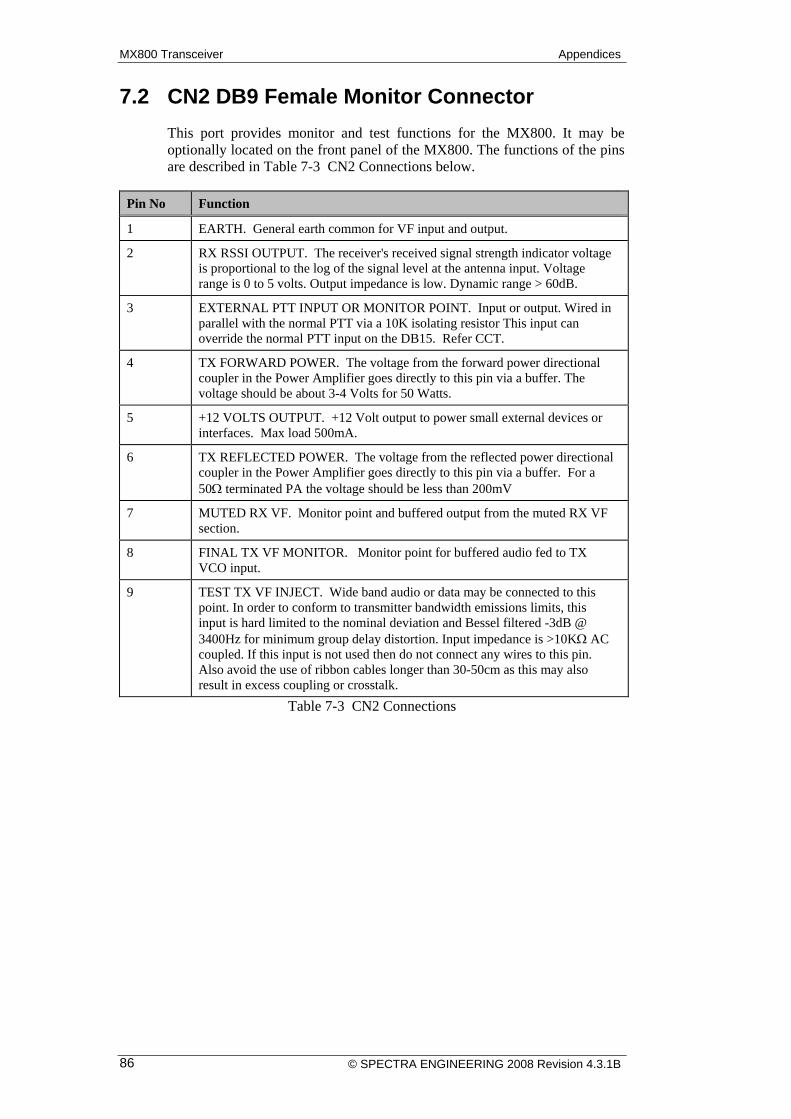
MX800 Transceiver Appendices
7.2 CN2 DB9 Female Monitor Connector This port provides monitor and test functions for the MX800. It may be optionally located on the front panel of the MX800. The functions of the pins are described in Table 7-3 CN2 Connections below.
Pin No Function
1 EARTH. General earth common for VF input and output.
2 RX RSSI OUTPUT. The receiver's received signal strength indicator voltage is proportional to the log of the signal level at the antenna input. Voltage range is 0 to 5 volts. Output impedance is low. Dynamic range > 60dB.
3 EXTERNAL PTT INPUT OR MONITOR POINT. Input or output. Wired in parallel with the normal PTT via a 10K isolating resistor This input can override the normal PTT input on the DB15. Refer CCT.
4 TX FORWARD POWER. The voltage from the forward power directional coupler in the Power Amplifier goes directly to this pin via a buffer. The voltage should be about 3-4 Volts for 50 Watts.
5 +12 VOLTS OUTPUT. +12 Volt output to power small external devices or interfaces. Max load 500mA.
6 TX REFLECTED POWER. The voltage from the reflected power directional coupler in the Power Amplifier goes directly to this pin via a buffer. For a 50Ω terminated PA the voltage should be less than 200mV
7 MUTED RX VF. Monitor point and buffered output from the muted RX VF section.
8 FINAL TX VF MONITOR. Monitor point for buffered audio fed to TX VCO input.
9 TEST TX VF INJECT. Wide band audio or data may be connected to this point. In order to conform to transmitter bandwidth emissions limits, this input is hard limited to the nominal deviation and Bessel filtered -3dB @ 3400Hz for minimum group delay distortion. Input impedance is >10KΩ AC coupled. If this input is not used then do not connect any wires to this pin. Also avoid the use of ribbon cables longer than 30-50cm as this may also result in excess coupling or crosstalk.
Table 7-3 CN2 Connections
© SPECTRA ENGINEERING 2008 Revision 4.3.1B 86

Technical Manual Appendices
7.3 CN3 DB25 Female Digital I/O Connector Each CMOS logic input is protected by a 10K Ohm series resistor to the input of the logic chip. There is also a 10K Ohm pull up/down resistor at each input so as to default the input value to that set by JMP19. Each logic output is protected by a 1K-Ohm series resistor from the output of the logic chip.
Pin No Function
13 DIGITAL EARTH or +5VDC output. JMP15 selectable.
25 INPUT PORT A. 8-bit Logic Input bit 0. (Power control bit 0)or Digital CTCSS Control bit 0
12 INPUT PORT A. 8-bit Logic Input bit 1. (Power control bit 1)or Digital CTCSS Control bit 1
24 INPUT PORT A. 8-bit Logic Input bit 2. (RX CTCSS control)or Digital CTCSS Control bit 2
11 INPUT PORT A. 8-bit Logic Input bit 3. (TX CTCSS control)or Digital CTCSS Control bit 3
23 INPUT PORT A. 8-bit Logic Input bit 4. (N/W address bit 0)
10 INPUT PORT A. 8-bit Logic Input bit 5. (N/W address bit 1)
22 INPUT PORT A. 8-bit Logic Input bit 6. (N/W address bit 2)
9 INPUT PORT A. 8-bit Logic Input bit 7. (N/W address bit 3)
21 INPUT PORT B. Channel Select BCD Units bit 0. / Binary Bit 0.
8 INPUT PORT B. Channel Select BCD Units bit 1. / Binary Bit 1.
20 INPUT PORT B. Channel Select BCD Units bit 2. / Binary Bit 2.
7 INPUT PORT B. Channel Select BCD Units bit 3. / Binary Bit 3.
19 INPUT PORT B. Channel Select BCD Tens bit 0. / Binary Bit 4.
6 INPUT PORT B. Channel Select BCD Tens bit 1. / Binary Bit 5.
18 INPUT PORT B. Channel Select BCD Tens bit 2. / Binary Bit 6.
5 INPUT PORT B. Channel Select BCD Tens bit 3. / Binary Bit 7.
17 OUTPUT PORT C. 8-bit Logic Output bit 7.
4 OUTPUT PORT C. 8-bit Logic Output bit 6.
16 OUTPUT PORT C. 8-bit Logic Output bit 5.
3 OUTPUT PORT C. 8-bit Logic Output bit 4.
15 OUTPUT PORT C. 8-bit Logic Output bit 3.(Digital CTCSS Control bit 3)
2 OUTPUT PORT C. 8-bit Logic Output bit 2. (Digital CTCSS Control bit 2)
14 OUTPUT PORT C. 8-bit Logic Output bit 1. (Digital CTCSS Control bit 1)
1 OUTPUT PORT C. 8-bit Logic Output bit 0. (Digital CTCSS Control bit 0)
Table 7-4 CN3 Connections
© SPECTRA ENGINEERING 2008 Revision 4.3.1B 87

MX800 Transceiver Appendices
© SPECTRA ENGINEERING 2008 Revision 4.3.1B 88
Note When the front panel channel select option is fitted, input port should not be used from the external connector CN3 as it is wired to the thumbwheel switch.
7.3.1 CN4 DB9 Male RS232 Connector
RS232 serial port to the MX800. It may be optionally located on the front panel of the MX800. Only 3 wires are required for the MX800 TXD, RXD and ground. The function of TXD and RXD pins can be interchanged by changing jumpers JMP10 and JMP11. Table 7-5 CN4 Connector Jumpers below illustrates this.
Name Function JMP 10/11
(Referred to MX800) 2-3 1-2
CN4 Pin no CN4 pin no
TD Transmitted Data 3 2
RD Received Data 2 3
SG Signal Ground 5 5
Table 7-5 CN4 Connector Jumpers
Note Both JMP10 and JMP11 must be set to the same positions. In position 2-3 the radio will require a serial cable with the TXD and RXD lines cross-connected. In position 1-2 a one to one cable is required.
7.3.2 CN6 Simplex Relay/External Reference
This is an N type connector, which acts as the RF I/O port for simplex operation. Optionally the RX input for duplex operation may use this port instead of the BNC port or if an external reference is required this port can be used.

Technical Manual Appendices
7.3.3 CN7 RX Input
This is a BNC connector used as the RX RF input.
7.3.4 CN8 TX Output
This is an N type connector used as the TX RF power output.
7.3.5 CN9 RJ45
This connector may optionally be fitted. The function depends upon which option board is fitted. A standard option is the isolated line I/O and this connector is used for this function when this option is fitted. See Options section for connection details.
A rectangular knock out section in the chassis provides for mounting of the connector should it be required.
7.3.6 CN5 DC Power Input
DC power is connected to the transceiver through this connector. The transceiver is fitted with a 3-pin male connector. For 50W transceivers pins 2 and 3 are used for the 12V DC pin 1 is unused. The power lead to the transceiver should be made from a gauge of wire suitable to ensure less than 0.5V drop at 10A for the required length of the lead.
PIN No Function
1 Unused
2 Ground
3 + 13.8VDC
Table 7-6 CN5 DC Power Input Connections
3
1
2
+ -
Figure 7-1 CN5 DC Input (View from rear of MX800)
© SPECTRA ENGINEERING 2008 Revision 4.3.1B 89

MX800 Transceiver Appendices
7.4 MX800 Specifications Minimum performance to exceed the following for 30 MHz to 960 MHz*:
AS4295-1995
ETS 300 086 Jan 1991,ETS 300 113
FCC Part 90
TIA/EIA-603
BAPT 225 ZV 1/2098 (German Soft keying)
CEPT T/R 24-01 E Sept 1988
EC Marking, EC EMC Directive 89/336/EEC
RFS25, RFS26, RFS32
*Conforms but may not be approved.
Consult Spectra Engineering regarding current type approvals and for latest and current MX800 Specification Data sheet.
7.4.1 Operating Frequency Bands
The MX800 is available in a number of models, which cover the range of operating frequency bands. As the transmitters and receivers are functionally independent the radios may be cross-banded if required. Refer to section 7.6 for details of the band breakdown.
7.4.2 General
Parameter Specification
MX800 Rack Size: 2RU Case, 330mm deep including fan.
MX800 Overall Physical Size 89mm high, 360mm deep, 483mm wide
Weight < 9kG
Supply Voltage: 13.8V +/- 20%.
Power Consumption: <600 mA receive, typical 460mA. (TX VCO off)
<11A for 50W TX RF @13.8VDC.
Operating Temperature: -10 to +60 C.
Individual Module Dimensions: TX & RX W=100, L=180, H = 30mm.
PA W=78, L=300, H = 60mm.
Standard LED indicators: Power, TX, RX, CTCSS, Aux, Alarm.
Speaker output 1 Watt
Frequency Range: Coverage 30-960 MHz.
Synthesis Method: Non mixing PLL Fractional N synthesiser.
Modulation: Direct FM, two point method
© SPECTRA ENGINEERING 2008 Revision 4.3.1B 90

Technical Manual Appendices
+/-2.5 kHz narrow band, +/- 5 kHz wide band
Channel Spacing: 50kHz, 30kHz, 25kHz, 20kHz or 12.5kHz.
Synthesiser Step Size: 25, 12.5,10, 7.5 or 6.25kHz.
Channels: 255 Software, DIP switch and rear port selectable.1-99 through rear port if configured for BCD parallel selection.
Table 7-7 General Specifications
7.4.3 Transmit
Measured in accordance with TIA/EIA-603 standards.
Parameter Specification
RF Power Output: 1W to 50W variable (30-520 MHz). 5W to 100W variable (135-174MHz)
0W to 1W (395-520MHz). (800-960 MHz).
Frequency Stability: 20PPM, 2.5PPM, 1.5PPM(std) or 1.0PPM.
Audio response: Flat within +1, -3dB across bandwidth
Audio Bandwidth VF input: 300Hz to 3400Hz Bessel LPF
Audio Bandwidth DC FM input: DC to 3400Hz base band (-3dB)
Modulation Distortion: Less than 2% at 60% deviation.
S/N Ratio: Better than 50dB, wide band.
Better than 44dB, narrow Band.
Spurii: Better than –90dBc.
RF Switching Bandwidth Exciter: Same as band allocation.
RF Switching Bandwidth PA: Band dependent , typ >35Mhz
Duty Cycle: 100% for 50W RF output with thermally controlled fan.
RF Rise Time: 4mS with continuous VCO selected (Controlled RF envelope).
Table 7-8 Transmit Specifications
© SPECTRA ENGINEERING 2008 Revision 4.3.1B 91

MX800 Transceiver Appendices
7.4.4 Receive
Measured in accordance with TIA/EIA-603 standards. Parameter Specification
Sensitivity: Better than -117dBm for 12dB (25 kHz spacing), De-emphasis. Typical -120dBm
Selectivity 30-50MHz: More than 90 dB for 25 kHz adj channel, More than 80 dB for 12.5 kHz adj channel.
Selectivity 66-520MHz: More than 80 dB for 25 kHz adj channel, more than 75 dB for 12.5 kHz adj channel,.
Selectivity 805-960MHz: More than 70 dB for 25 kHz adj channel more than 65 dB for 12.5 kHz adj channel.
Spurious Resp: Better than 90dB.
Intermodulation: Better than 80dB.@ 100kHz/200kHz offset
Blocking: Better than 100dB at +/- 1MHz point.
Distortion: Less than 2% at 60% deviation.
S/N Ratio: Better than 50dB wide band. Better than 44dB narrow band.
Receiver Front End BW: Equal to band allocation, no retuning.
Discriminator Audio Bandwidth: DC to 3400Hz (-3dB)
Audio Bandwidth VF output:
300Hz to 3000Hz, +1/-3dB
Squelch Opening Time: Less than 20mS @ 20dB SINAD.
Squelch Closing Time: Less than 100mS.
Conducted Spurious: Less than -57dBm, typ -90dBm.
Table 7-9 Receive Specification
© SPECTRA ENGINEERING 2008 Revision 4.3.1B 92

Technical Manual Appendices
7.4.5 Ancillaries
Parameter Specification
TX Timer: Programmable, on/off selectable
VF Level to Line: +6 to -15dBm, 600 ohms unbalanced or differential
VF Level from Line: +6 to -15dBm, 600 ohms unbalanced, with Compressor enabled.
Pre-Emphasis Accuracy: Within +1,-3dB of 6dB per octave curve
De-Emphasis Accuracy: Within +1,-3dB of 6dB per octave curve
VF Compressor Range: >30dB for line input
Digital Outputs: 1K-ohm 5V source/sink available
Alarm Output: Open collector
PTT Input: +5V Logic active low
Channel Select: 8 way Dip switch or RS232 or BCD/Binary
Repeater Tail Timer: Programmable
Table 7-10 Ancilary Specifications
7.5 Channel Select DIP Switch Settings Refer to section 2.2.2.3 for a description on the alternative methods to select the operating channel. If a hardware channel select method is chosen the following table shows how to set the switches for each channel. Select the fixed channel for the MX800 by using the DIP switch DIP1 located on the Micro Controller Board. Channel 1 to 255 is available in binary selection. Switch position 1 is channel 1, position 2 is channel 2, position 3 is channel 4, position 4 is channel 8, position 5 is channel 16, position 6 is channel 32, position 7 is channel 64, position 8 is channel 128.
A table of DIP switch 1 settings follows, where switch ON is indicated by an "x" in a cell and no entry in a cell represents a switch OFF.
CH
SW1
SW3
SW4
SW5
SW6
SW8
CH
SW1
SW3
SW4
SW5
SW6
SW2
SW7
SW2
SW7
SW8
0 13 X X X 1 X 14 X X X 2 X 15 X X X X 3 X X 16 X 4 X 17 X X 5 X X 18 X X 6 X X 19 X X X 7 X X X 20 X X 8 X 21 X X X 9 X X 22 X X X 10 X X 23 X x X X 11 X x X 24 X X 12 X X 25 X X X
© SPECTRA ENGINEERING 2008 Revision 4.3.1B 93

MX800 Transceiver Appendices
© SPECTRA ENGINEERING 2008 Revision 4.3.1B 94
CH
SW1
SW2
SW3
SW4
SW5
SW6
SW7
SW8
CH
SW1
SW2
SW3
SW4
SW5
SW6
SW7
SW8
26 X X X 79 X X X X X 27 X X X X 80 X X 28 X X X 81 X X X 29 X X X X 82 X X X 30 X X X X 83 X X X X 31 X X X X X 84 X X X 32 X 85 X X X X 33 X X 86 X X X X 34 X X 87 X X X X X 35 X X X 88 X X X 36 X X 89 X X X X 37 X X X 90 X X X X 38 X X X 91 X X X X X 39 X X X X 92 X X X X 40 X X 93 X X X X X 41 X X X 94 X X X X X 42 X X X 95 X X X X X X 43 X X X X 96 X X 44 X X X 97 X X X 45 X X X X 98 X X X 46 X X X X 99 X X X X 47 X X X X X 100 X X X 48 X X 101 X X X X 49 X X X 102 X X X X 50 X X X 103 X X X X X 51 X X X X 104 X X X 52 X X X 105 X X X X 53 X X X X 106 X X X X 54 X X X X 107 X X X X X 55 X X X X X 108 X X X X 56 X X X 109 X X X X X 57 X X X X 110 X X X X X 58 X X X X 111 X X X X X X 59 X X X X X 112 X X X 60 X X X X 113 X X X X 61 X X X X X 114 X X X X 62 X X X X X 115 X X X X X 63 X X X X X X 116 X X X X 64 X 117 X X X X X 65 X X 118 X X X X X 66 X X 119 X X X X X X 67 X X X 120 X X X 68 X X 121 X X X X X 69 X X X 122 X X X X X 70 X X X 123 X X X X X X 71 X X X X 124 X X X X X 72 X X 125 X X X X X X 73 X X X 126 X X X X X X 74 X X X 127 X X X X X X X 75 X X X X 128 X 76 X X X 129 X X 77 X X X X 130 X X 78 X X X X 131 X X X

Technical Manual Appendices
© SPECTRA ENGINEERING 2008 Revision 4.3.1B 95
CH
SW1
SW2
SW3
SW4
SW5
SW6
SW7
SW8
CH
SW1
SW2
SW3
SW4
SW5
SW6
SW7
SW8
132 X X 185 X X X X X 133 X X X 186 X X X X X 134 X X X 187 X X X X X X 135 X X X X 188 X X X X X 136 X X 189 X X X X X X 137 X X X 190 X X X X X X 138 X X X 191 X X X X X X X 139 X X X X 192 X X 140 X X X 193 X X X 141 X X X X 194 X X X 142 X X X X 195 X X X X 143 X X X X X 196 X X X 144 X X 197 X X X X 145 X X X 198 X X X X 146 X X X 199 X X X X X 147 X X X X 200 X X X 148 X X X 201 X X X X 149 X X X X 202 X X X X 150 X X X X 203 X X X X X 151 X X X X X 204 X X X X 152 X X X 205 X X X X X 153 X X X X 206 X X X X X 154 X X X X 207 X X X X X X 155 X X X X X 208 X X X 156 X X X X 209 X X X X 157 X X X X X 210 X X X X 158 X X X X X 211 X X X X X 159 X X X X X X 212 X X X X 160 X X 213 X X X X X 161 X X X 214 X X X X X 162 X X X 215 X X X X X X 163 X X X X 216 X X X X 164 X X X 217 X X X X X 165 X X X X 218 X X X X X 166 X X X X 219 X X X X X X 167 X X X X X 220 X X X X X 168 X X X 221 X X X X X X 169 X X X X 222 X X X X X X 170 X X X X 223 X X X X X X X 171 X X X X X 224 X X X 172 X X X X 225 X X X X 173 X X X X X 226 X X X X 174 X X X X X 227 X X X X X 175 X X X X X X 228 X X X X 176 X X X 229 X X X X X 177 X X X X 230 X X X X X 178 X X X X 231 X X X X X X 179 X X X X X 232 X X X X 180 X X X X 233 X X X X X 181 X X X X X 234 X X X X X 182 X X X X X 235 X X X X X X 183 X X X X X X 236 X X X X X 184 X X X X 237 X X X X X X

MX800 Transceiver Appendices
SW2
SW3
SW4
SW6
SW7
CH
SW3
SW3
SW1
SW5
SW8
SW1
SW4
SW5
SW6
CH
SW7
SW8
238 X X X X X X 247 X X X X X X X 239 X X X X X X X 248 X X X X X 240 X X X X 249 X X X X X X 241 X X X X X 250 X X X X X X 242 X X X X X 251 X X X X X X X 243 X X X X X X 252 X X X X X X 244 X X X X X 253 X X X X X X X 245 X X X X X X 254 X X X X X X X 246 X x X X X X 255 x X x X X X X X
© SPECTRA ENGINEERING 2008 Revision 4.3.1B 96

Technical Manual Appendices
© SPECTRA ENGINEERING 2008 Revision 4.3.1B 97
Notes:1. Band E, L2, R3, Q2 receive only2. Band E2, R2, V2 transmit only3.° Standard Preferred Frequency Band. 4. Band A2, A3: 4 MHz Rx VCO Sw BW5. * 100W only available in 135 -175Mhz.
7.6 MX800 Model Number Configuration Guide The MX800 build can be specified by the model number. The diagram below shows how the model number is derived from the wanted options. Consult Spectra for availability details on specific configurations and options.
Due to ongoing development please refer to www.spectraeng.com.au for the latest revision of this document page.
Band Frequency A2 30-39 MHz A3 39-50 MHz A 66-80 MHz B° 70-88 MHz C 135-160 MHz D 155-180 MHz D3° 148-174 MHz E 177-207 MHz E2 177-185 MHz F 195-225 MHz G 220-250 MHz H 245-275 MHz I 270-300 MHz J 295-325 MHz J2 300-337 MHz K 320-350 MHz L 345-375 MHz M 370-400 MHz N 395-430 MHz N2° 400-435 MHz O 425-460 MHz O2 435-470 MHz P 455-490 MHz P2° 450-485 MHz P3 475-495MHz Q° 485-520 MHz Q2 500-532 MHz Q3 485-505 MHz
Band Frequency R 805-825 MHz R2 746-764 MHz R3 776-794 MHz S 824-849 MHz T 850-870 MHz U 872-905 MHz V 890-915 MHz V2 900-925 MHz W 917-950 MHz X 925-960 MHz Z None
Front PanelS StandardC Custom
RF ConfigD DuplexS Simplex
MX800
Controller OptionsZ Standard ControllerL LC Controller
Frequency Stability1 1.0 ppm (-30 to 60°C)2° 1.5 ppm (-10 to 60°C) & 2.5 ppm (-30 to -10°C)4 20 ppm (-30 to 60°C)5 2.5 ppm (-10 to 60°C) & 5 ppm (-30 to -10°C)
OptionsZ No optionsS Options fitted (Specify separately)
Channel AllocationN 12.5 kHz (Narrow)M 20 kHz (Medium)W 25 kHz (Wide)D 30 kHz (Data)C 50 kHz (Cellular)P 12.5/25 kHz Programmable
TX PowerE 1 Watt (Extra Low, Bands N - Q)L 5 Watt (Low, N - Q3)N 15 Watt (800 MHz Normal)I 25 Watt (Intermediate)M 35 Watt (800 MHz Medium)H 50 Watt (High)V 100 Watt (Very High)Z None
Rx FreqTx Freq

MX800 Transceiver Appendices
7.7 MX800 System Applications Comprehensive standard features along with a wide range of options and accessories available to it mean that the MX800 is capable of being used in many different applications. The most common of which are mentioned below together with notes where applicable on the relevant aspect of the MX800.
Figure 7-2 MX800’s Setup in system rack
7.7.1 Conventional base station/repeater
Upper tier RF performance figures make the MX800 an excellent choice for a conventional base station or repeater. The PA is continuously rated and receiver figure of merit parameters such as sensitivity, Intermodulation and selectivity are all of a high standard. Independently adjustable PTT and CTCSS tails mean that the mute crash can be eliminated in mobiles when base transmit CTCSS is used. A 40ms RX audio delay option (T08) similarly facilitates the elimination of the mute crash in the base station side.
As standard feature when the CTCSS encode/decode option is selected is multiple tone groups. In excess of 25 tones can be selected as valid CTCSS tones on a shared RF channel. Provision is made in the programming software to enter tone pairs for each group without restriction on how the tones are selected.
Many other attributes of the MX800 and its options are useful in conventional base/repeater systems. For example:-
♦ Programmable channel bandwidth ♦ DCS / Digital Private Line ♦ Range of front panel functions available ♦ Optional two wire four wire operation ♦ Tone PTT with programmable PTT tone ♦ Optional balanced and isolated VF I/O and signaling lines
© SPECTRA ENGINEERING 2008 Revision 4.3.1B 98

Technical Manual Appendices
7.7.2 Link transceiver
In the UHF bands (400 to 520 MHz) the MX800 is available in 1W and 50W. The 1W version being intended for link transceiver application. Transmit and receive audio is conveniently brought out to the D15 connector on the rear of the radio along with the mute and PTT signals. In addition, provision is made to inject an Analog CTCSS tone into the transmit leg of the link and a 300Hz low pass filtered CTCSS signal is available at the RX leg of the link to recover the tone. Hence the Analog CTCSS tone can be transferred (or cross banded) from one MX800 to another. On an RF path with good signal to noise ratio, this enables CTCSS synchronization across the link in the situation where multiple tone group operate at two different sites. Spectra Engineering plans to upgrade this function with a digital 4 bit interface such that the operating CTCSS group is decoded at the repeater and re-encoded or cross encoded across the link, and the process repeated in reverse at the remote end.
7.7.3 Data transceiver
The MX800 transmit audio path is user configurable to a very large degree. TX modulation signals can be injected with or without processing depending upon the individual application. The transmitter low pass filter (the deviation limiter which sets the modulation bandwidth and ensures compliance with regulatory requirements) is a Bessel filter with linear phase characteristics. Fast transmitter key-up time and mute action mean reduced signalling turn around overheads for data messages and better throughput especially in a Simplex system with predominantly short messages.
7.7.4 Paging transmitter
Due to the two point modulation method employed in the MX800, the transmit modulation frequency response can go down to DC as correctly required for POCSAG or other FSK based modulation systems. In addition it has a DC coupled FM modulator input biased to a voltage of 2.5 volts for carrier frequency Fo. A square wave input signal of 0 to 5V injected on this point drives the modulator to the positive and negative extremes of the deviation limiter. In this case set to +/- 4.5kHz. This means that it can transmit typical POCSAG paging signals. The modulation rise time is controlled by the frequency response of the transmit audio path low pass filter and is suitable for data rates of up to 2400 baud.
A typical system arrangement is shown in drawing SC004-1A.
SYSTEM ALIGNMENT
The FSK link deviation should be set to 60% of maximum deviation.
The paging transmitter alignment is similar to the standard alignment in paragraphs 5.1.9 and 5.1.10 in the MX800 technical manual. In 5.1.9 “Procedure” item 3 set the peak deviation to +/-4.5kHz (instead of +/-4.8kHz). In item 5 set the TX modulation frequency to half the data rate of the POCSAG data e.g. 600Hz for 1200-baud data etc.
© SPECTRA ENGINEERING 2008 Revision 4.3.1B 99

MX800 Transceiver Appendices
Other than these changes the TX alignment is as per the technical manual.
7.7.5 Trunking Base Station
The MX800 is widely used as a trunking base station. A one hundred percent continuously rated transmitter is vital in the high duty cycle environment of a trunking systems. MPT 1327 control channels are permanently keyed up. Optionally the FSK signalling of MPT systems can be injected flat into an non pre-emphasized input and received on an non de-emphasized output which allows the signalling to go flat to air. As a compact two RU height enclosure the MX800 permits a high channel density for a given rack height.
LTR trunking systems make use of a digital sub audible signalling scheme. Once again the low frequency modulation capabilities (down to DC) of MX800 are vital in ensuring that the signalling takes place and a low bit error rate. A marginal system will result if the Transmitter modulation response can not go below 10Hz.
7.7.6 Systems base
Typical small systems environments. Once again the user interface presented at the rear of the radio and the software programmable functions through MXTOOLS give systems designers and large degree of control over the base station.
In a system, which operates in one RF band, it is particularly convenient and cost-effective if all base stations can be made and programmed identically. This reduces the number of spare base stations required to maintain the system. MX800 supports this mode of operation in as much as the operating characteristics of up to 255 channels can be pre-programmed in all of the base stations, and insertion of an on-site channel selector and configuration plug selects the particular operating parameters for that base station in that location. Spectra will introduce additional features in this area.
7.7.7 Repeater with Morse ID
A programmable built in Morse ID encoder makes it convenient to use the MX800 as a UHF CB repeater, Amateur repeater or auto identified repeater.
7.7.8 Simplex base station
Option T06 for the MX800 is a coaxial changeover relay. In a Simplex system with a single antenna and common transmit and receive frequencies this can be used for connection of the transmitter and or receiver to the antenna. Provision is made in the programming to introduce a 50ms delay on transmit to allow the relay to changeover prior to RF ramp up.
© SPECTRA ENGINEERING 2008 Revision 4.3.1B 100

Technical Manual Appendices
7.7.9 Duplicated base station
Spectra engineering has current plans for the development of an Automatic Changeover Units to facilitate duplicated base station operation.
This option is not currently available. Due to ongoing development please refer to www.spectraeng.com.au for the latest information regarding this option.
7.7.10 Power Save base station
For solar powered sites and other power critical applications the MX800 is capable of a Power Save (Low Standby Current) Mode. This option can be implemented in three stages. Stage one implementation replaces the micro controller linear voltage regulators with switching regulators. Response times are unaffected. Stage two involves removing power from the exciter when the radio is in standby mode. In this case RX responses times are unaffected. In stage three the RX power is cycled on and off at a user selectable duty cycle. Essentially the choice of mode of operation involves a compromise between response time and average current consumption. Current consumption of 250mA is achievable with a typical response time in the order of 1sec.
7.7.11 Tone key base station
T19/T26 is a new Spectra Engineering development, which incorporates a number of features and functions, of which are covered in Error! Reference source not found.
7.7.12 Voting base station
As noted in section 3.15 the MX800 with option T19 can provide a Variable tone encoder. This encoder is compatible with a commonly used Variable tone-voting arbitrator.
MX800 can also be used with a SINAD voting arbitrator. Mute status of the receiver can optionally be signalled to the voting arbitrator via tone or through DC key E & M signalling.
Spectra engineering has current plans to implement the base station component of a race voting system using a Central arbiter.
7.7.13 Simulcast base station
Precise control of transmitter RF frequency is essential in simulcasts systems. Option T12 provides an external TX reference oscillator input for injection of highly stable oscillator. Almost any frequency may be injected.
In addition, each transmitter channel frequency can be offset individually by small amounts if the internal reference frequency is used. The 1PPM frequency Stability option is specified for a minimum of 8PPM adjustment.
© SPECTRA ENGINEERING 2008 Revision 4.3.1B 101

MX800 Transceiver Appendices
Take care if too much offset is used as this may effect the modulation symmetry. The use of this feature and a low frequency carrier dithering has proven to eliminate the previous requirements of extremely high stability reference frequency inputs.
The MX800 has been widely installed for the use in simulcast systems. These DSP based systems provide automatic compensation for changes in modulation delay characteristics.
The T36 Option extends the modulation capabilities of the MX800 when an externally locked reference input signal is required. In Simulcast systems where the application does not just require just Voice modulation but also the additional capability of either Data, POCSAG, CTCSS or DCS, then a transmitter is required to have a modulation bandwidth that extends to down towards 5Hz or better still to DC (0Hz). This new option provides that capability by incorporating digital RF techniques. In addition, the carrier can be offset in each transmitter in steps of 1Hz.
Drawing No. Description
SC001-1A MX800 Conventional Systems Examples
SC001-2A MX800 Conventional Systems Examples
SC003-1A MX800 T19/T26 option Board Example
SC004-1A MX800 Paging Configuration Example
SC006-1A MX800 Link System Configuration Example
© SPECTRA ENGINEERING 2008 Revision 4.3.1B 102

Technical Manual Appendices
© SPECTRA ENGINEERING 2008 Revision 4.3.1B 103
TITL
EM
X800
Con
vent
iona
l Sys
tem
s Ex
ampl
es
SPE
CTR
A EN
GIN
EER
ING
PTY
LTD
DR
AW
NA
JCC
08/0
3/04
SHEE
T1
0F 1
DAT
EAP
PRO
VED
AD
OC
No
SC00
1-1A
REV
CH
ECKE
D
MX
800
Con
vent
iona
l rep
eate
r Sys
tem
s
Por
tabl
es a
nd m
obile
s un
its
MX
800
Tran
scei
ver
?

MX800 Transceiver Appendices
© SPECTRA ENGINEERING 2008 Revision 4.3.1B 104
TITL
EM
X80
0 C
onve
ntio
nal S
yste
ms
Exa
mpl
es
SPEC
TRA
EN
GIN
EER
ING
PTY
LTD
DR
AWN
AJC
C
08/0
3/04
SHEE
T1
0F 1
DAT
EA
PPR
OV
ED
AD
OC
No
SC
001-
2AR
EVC
HEC
KED
DUP
LINK
DU
P
REP
DU
P
REP
LINK
DUP
DU
P
REP
DU
P
REP
Two
MX
800
Con
vent
iona
l rep
eate
rSy
stem
s lin
ked
toge
ther
(Bac
k To
Bac
k R
epea
ters
)
Two
MX8
00 C
onve
ntio
nal r
epea
ter S
yste
ms
linke
d to
geth
er v
ia a
RF
link
usin
g M
X800

Technical Manual Appendices
© SPECTRA ENGINEERING 2008 Revision 4.3.1B 105
TITL
EM
X80
0 B
AC
K T
O B
ACK
LIN
K D
IAG
RA
M
SPE
CTR
A E
NG
INE
ERIN
G P
TY L
TDD
RAW
NA
JCC
04/1
1/04
SHE
ET1
0F 1
DAT
EAP
PRO
VED
AD
OC
No
SC
002-
1AR
EV
CH
EC
KED
MX
800
Uni
t A
MX8
00 R
EAR
PA
NEL
DB
15F
LIN
E I/O
1513
119
75
31
144
68
1012
2
RX AUDIO 5 OHMS
16
12
34
56
78
914
1312
1110
15
SKHC
N1
ALARM O/P # 1/M LEAD
TX VF LOOPBACK CTRL
RX DISCRIMINATOR
ALARM O/P # 2
ALARM O/P # 3
TX AUDIOREPEATER ENABLE
RX TALK
EARTHTX TALK
RX AUDIO 600 OHMSRX MUTE/
DC FM / WB I/PPTT M
X80
0U
nit B
INTE
RFA
CE
PCB
E(b)E(a)
TX VF (b)RX leg (b)
Tx VF (a)Rx VF (b)
M (COM)M (NC)
12
34
56
78
RJ4
5 8P
8C S
ocke
t
RJ4
5 8P
8C S
ocke
t
MX8
00 R
EAR
PA
NEL
DB
15F
LIN
E I/O
1513
119
75
31
144
68
1012
2
RX AUDIO 5 OHMS
16
12
34
56
78
914
1312
1110
15
SKHC
N1
ALARM O/P # 1/M LEAD
TX VF LOOPBACK CTRL
RX DISCRIMINATOR
ALARM O/P # 2
ALARM O/P # 3
TX AUDIOREPEATER ENABLE
RX TALK
EARTHTX TALK
RX AUDIO 600 OHMSRX MUTE/
DC FM / WB I/PPTT
INTE
RFA
CE
PCB
E(b)E(a)
TX VF (b)RX leg (b)
Tx VF (a)Rx VF (b)
M (COM)M (NC)
12
34
56
78
RJ4
5 8P
8C S
ocke
t
RJ4
5 8P
8C S
ocke
t

MX800 Transceiver Appendices
© SPECTRA ENGINEERING 2008 Revision 4.3.1B 106
TITL
EM
X80
0 T1
9/26
Exa
mpl
e of
sys
tem
con
figur
atio
n
SPE
CTR
A E
NG
INE
ERIN
G P
TY L
TDD
RAW
NA
JCC
06/0
9/04
SHE
ET1
0F 1
DAT
EAP
PRO
VED
AD
OC
No
SC
003-
1AR
EV
CH
EC
KED
MX
800
Fitte
d w
ithT1
9/T2
6 op
tion
Boa
rds
2 or
4 W
ire L
ine
Inte
rface
SITE
ASI
TE B
Exam
ple
of s
yste
m c
onfig
urat
ion
Por
tabl
es a
nd m
obile
s un
its
Por
tabl
es a
nd m
oblie
uni
ts
This
allo
w m
obile
s an
d po
rtabl
e fro
m S
ite A
to ta
lk to
Uni
ts in
Site
B
MX8
00Fi
tted
with
T19/
T26
optio
n Bo
ards
E &
M C
ontro
lled
by T
ones
or I
sola
ted
inte
rface

Technical Manual Appendices
© SPECTRA ENGINEERING 2008 Revision 4.3.1B 107
TITL
EM
X80
0 P
agin
g C
onfig
urat
ion
Exa
mpl
e
SPE
CTR
A E
NG
INE
ERIN
G P
TY L
TDD
RAW
NA
JCC
06/0
9/04
SHE
ET1
0F 1
DAT
EAP
PRO
VED
AD
OC
No
SC
004-
1AR
EV
CH
EC
KED
MX
800
RX
FSK
Mod
em
MX
800
TX
0 to
5V
PO
CS
AG
sig
nal t
o D
C F
Min
put.
MX
800
uses
repe
ater
PTT
.R
epea
t VF
sour
ce s
et to
Lin
e.
IBM
Com
patib
le
Pag
ing
Enc
oder
Mod
emMX
800T
X
PTT
act
ive
low
5V
Cm
os c
ompa
tible
V23
FSK
tone
s RS
232
Dig
ital P
OC
SA
Gbi
t stre
am
TX o
nly
MX
800
Pag
ing
term
inal

MX800 Transceiver Appendices
© SPECTRA ENGINEERING 2008 Revision 4.3.1B 108
TITL
EM
X80
0 Li
nk S
yste
m C
onfig
urat
ion
Exam
ple
SPE
CTR
A E
NG
INE
ERIN
G P
TY L
TDD
RAW
NA
JCC
06/0
9/04
SHE
ET1
0F 1
DAT
EAP
PRO
VED
AD
OC
No
SC
006-
1AR
EV
CH
EC
KED
DUP
LINK
DU
P
REP
DUP
LINK
DU
P
REP
Brid
ge
LINK
DUP
DU
P
REP
LINK
DUP
This
sect
ion
illus
trate
s a M
X80
0 re
peat
er c
onne
cted
totw
o lin
k tra
nsce
iver
s. F
or th
is ty
pe o
f con
nect
ion
and
audi
o br
idge
is re
quire
d su
ch a
s the
Om
nitro
nics
type
619
.
This
sect
ion
illus
trate
s and
MX
800
conn
ecte
d to
a li
nktra
nsce
iver
. All
that
is re
quire
dfo
r thi
s typ
e of
con
nect
ion
is a
back
-to-b
ack
cabl
e be
twee
n th
elin
k tra
nsce
iver
and
the
repe
ater
trans
ceiv
er
This
sect
ion
illus
trate
s and
MX
800
conn
ecte
d to
a li
nktra
nsce
iver
. All
that
is re
quire
dfo
r thi
s typ
e of
con
nect
ion
is a
back
-to-b
ack
cabl
e be
twee
n th
elin
k tra
nsce
iver
and
the
repe
ater
trans
ceiv
er

Technical Manual
8. Superseded Technical Information
8.1 Power Amplifier Module
8.1.1 Technical Description
RF from the Exciter on CN1 is first attenuated by a 50-ohm pad, which is used to provide good 50-ohm source impedance for the high power hybrid amplifier IC1. The RF is amplified to between 5 and 13 watts at the hybrid 50-ohm output. The signal from the hybrid is then matched by a broadband network to drive the low input impedance associated with the final transmit power amplifier transistor TR1. The transistor's low collector impedance is then also matched back to 50 ohms by a broadband matching network. Trimmer capacitors enable adjustment of the power amplifier over a wide bandwidth so as to maintain good conversion efficiency. Prior to transmission a low loss 13 element elliptical low pass filter, filters out the unwanted harmonics to less than -90dBc.
A dual directional coupler consists of coupled microstrip transmission lines S5, S6 and S7 fabricated on the PCB artwork. The sampled RF energy is rectified to provide a proportional DC voltage output on CN4-8 (FWD) and CN4-5 (REFL).
TR2 serves to switch the DC supply to the Hybrid under control of the PTT line from the Micro Controller on CN4-2. A thermistor TS1, physically located on the PA heatsink to monitor the heatsink temperature, is connected to the Micro Controller via CN4-4/6
8.1.2 PA Module Test Procedure
Test Equipment:
Tested MX800 with PA removed
PC with MXTOOLS software
RF Power Meter
RF Signal Generator
Multimeter
+13.8VDC 15A power supply
Preliminaries:
Program upper, middle and lower frequencies of band into 3 channels in MXTOOLS channel screen. Although the PA will function over a wider bandwidth, the nominal switching bandwidth of the PA is 10MHz. The recommended procedure is to centre this 10MHz around the centre of the user
© SPECTRA ENGINEERING 2008 Revision 4.3.1B 109

MX800 Transceiver Superseded Technical Information
frequencies. (Note that 'Continuous Update Enabled' on the MXTOOLS channel screen should be ticked for these tests)
Do not connect Exciter RF drive output CN1 to PA.
Procedure:
1. Remove PA top cover. Measure resistance of thermistor between CN4-6 and CN4-4, this should be approximately 2kΩ. Connect DC power lead and 10-way connector from MX800. Connect PA RF output to RF power meter and PA RF input (CN1) to RF signal generator.
2. Set signal generator to centre frequency of PA under test and reduce RF drive level (from signal generator) to zero. Switch DC power on and check that supply is present on L9. Assert PTT (check that no output RF power is emitted from the PA) check that the 13.8V supply is switched through to the Hybrid on pin adjacent to RF input and that 5V is switched to the Hybrid on the next pin along (pins not numbered on Hybrid).
3. With PTT ON measure the PA bias current at the Gates of the FET’s. The Bias current is band dependent. This is done by monitoring the current drain of the whole PA with CN1 disconnected. Link the gate of TR2 to GND. Measure current consumption (VHF High Band 200mA ,UHF 400mA.) This can be adjusted by RV2. Measure gate volts ≈ 3.4V Remove link from TR2. Measure current consumption, adjust RV1 so that current is 2Amp total (VHF & UHF). Measure gate volts ≈ 3.9V
4. With PA transmitting at 50W into 50Ω load measure DC volts FWD power sense CN4-8 and REFL power sense CN4-5. These voltages should be approx. 2.8V and <250mV respectively. Reduce RF drive until PA output is 10W and disconnect PA RF output cable. Measure DC voltage on CN4-8 and CN4-5 again. These should now both read lower approximately 1V. Remove PTT.
© SPECTRA ENGINEERING 2008 Revision 4.3.1B 110

Technical Manual Superseded Technical Information
8.1.3 PA Fault Finding Procedure
First do a visual check of all the components on the PA looking for any damaged components.
Connect the input of the PA to signal generator with the RF output switched off.
With PTT off measure the +13.8V supply at the collector of the output transistor.
Key up the PA and check the supply voltages on the hybrid module. Refer to your circuit diagram for test points.
Turn the supply voltage OFF and lift the RF output lead of the hybrid and solder a flying lead to the lifted leg. Connect the earth of the flying lead to the earth of the PA.
Connect the Flying lead to a power meter. Turn ON the supply voltage and the signal generator RF output, PTT the PA and increase the generator output whilst measuring the hybrid power output.
The hybrid may be faulty if it has an output of less than 5W.
The PA RF transistor may be faulty if the hybrid has an output power of greater than 5W.
See section 9.1 for superseded PA Drawings document number
© SPECTRA ENGINEERING 2008 Revision 4.3.1B 111

MX800 Transceiver Superseded Technical Information
This page left blank intentionally
© SPECTRA ENGINEERING 2008 Revision 4.3.1B 112

Technical Manual
9. Drawings Drawing No. Description Band
BD001-1 Receiver Block Diagram All
BD002-1 Exciter Block Diagram All
BD003-1/2 Micro Controller Block Diagram All
BD004-1 Power Amplifier Block Diagram All
IC001-1 MX800 Interconnection Diagram All
CS001-1/6 Micro Controller Board Circuit Diagram All
CS002-1 Exciter Circuit Diagram All
CS003-2 Receiver Front End Circuit Diagram All
CS004-2B TX VCO Circuit Diagram A to H
CS012-1 RX VCO Circuit Diagram R to X
CS015-1/2 Receiver Module Mixer and Programmable 45MHz IF
Section
A & B
CS016-1 Power Amplifier 50W Circuit Diagram A & B
CS017-1/2 Receiver Module Mixer and Programmable IF Section All except A3, A&B
bands.
CS018-1 Isolated Interface Option All
CS021-1 Trunk Interface Circuit diagram All
CS022-1 T11 option PCB Circuit diagram All
CS023-1 HP Rx VCO Circuit Diagram A to Q
CS025-1/2 Receiver Module Mixer and Programmable 70 MHz IF
Section
A3
CS028-1 Wide Band Power Amplifier 50W Circuit Diagram R2
CS029-1 Wide Band Power Amplifier 50W Circuit Diagram N to Q
CS031-1 Wide Band Power Amplifier 50W Circuit Diagram A to B
CS033-1 Wide Band Power Amplifier 50W Circuit Diagram K to M
CS035-1 T29 isolated interface Circuit Diagram ALL
CS038-1 Wide Band Power Amplifier 50W Circuit Diagram C to D3
CS039-1 Wide Band Power Amplifier 50W Circuit Diagram E to G
CS040-1 Wide Band Power Amplifier 50W Circuit Diagram H to J2
CS041-1 Wide Band Power Amplifier 50W Circuit Diagram A2
CS042-2 Wide Band Power Amplifier 50W Circuit Diagram A3
CS053-1 V3 RX VCO Circuit Diagram J-W
CS052-1 V3 TX VCO Circuit Diagram I-Q
© SPECTRA ENGINEERING 2008 Revision 4.3.1B 113
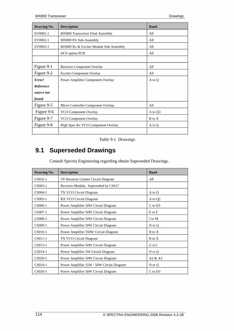
MX800 Transceiver Drawings
Drawing No. Description Band
EV0001-1 MX800 Transceiver Final Assembly All
EV0002-1 MX800 PA Sub-Assembly All
EV0003-1 MX800 Rx & Exciter Module Sub-Assembly All
DCS option PCB All
Figure 9-1 Receiver Component Overlay All
Figure 9-2 Exciter Component Overlay All
Error!
Reference
source not
found.
Power Amplifier Component Overlay A to Q
Figure 9-5 Micro Controller Component Overlay All
Figure 9-6 VCO Component Overlay A to Q3
Figure 9-7 VCO Component Overlay R to X
Figure 9-8 High Spec Rx VCO Component Overlay A to Q
Table 9-1 Drawings
9.1 Superseded Drawings Consult Spectra Engineering regarding obtain Superseded Drawings.
Drawing No. Description Band
CS032-1 VF Receiver Limiter Circuit Diagram All
CS003-1 Receiver Module, Superseded by CS017
CS004-1 TX VCO Circuit Diagram A to Q
CS005-1 RX VCO Circuit Diagram A to Q2
CS006-1 Power Amplifier 50W Circuit Diagram C to D3
CS007-1 Power Amplifier 50W Circuit Diagram E to F
CS008-1 Power Amplifier 50W Circuit Diagram J to M
CS009-1 Power Amplifier 50W Circuit Diagram N to Q
CS010-1 Power Amplifier 350W Circuit Diagram R to X
CS011-1 TX VCO Circuit Diagram R to X
CS013-1 Power Amplifier 50W Circuit Diagram G to I
CS014-1 Power Amplifier 5W Circuit Diagram N to Q
CS020-1 Power Amplifier 50W Circuit Diagram A2 & A3
CS024-1 Power Amplifier 25W / 50W Circuit Diagram N to Q
CS026-1 Power Amplifier 50W Circuit Diagram C to D3
© SPECTRA ENGINEERING 2008 Revision 4.3.1B 114