spintronics for low-power computing · spintronics is a technology which exploits the spin (rather...
TRANSCRIPT
Spintronics for Low-Power Computing
Yue Zhang1, 2, Weisheng Zhao1, 2*, Jacques-Olivier Klein1, 2, Wang Kang1, 3, Damien Querlioz1, 2, Youguang Zhang3, Dafiné Ravelosona1, 2 and Claude Chappert1, 2
1. IEF, Univ. Paris-Sud, Orsay, 91405, France
2. CNRS, UMR8622, Orsay, 91405, France 3. Electronics and Information Engineering, Univ. Beihang, Beijing, 100191, China
*Email: [email protected]
Abstract— Microelectronics has been following Moore's law for almost 40 years. However this trend tends to run out of steam in recent technology nodes. The continuous improvements in the size of the transistors and in the operating frequencies result in serious power consumption, heat dissipation and reliability issues. Spintronics (Nobel Prize of Physics, 2007 awarded to Prof. Fert from Univ. Paris-Sud and Peter Grünberg from Forschungszentrum Jülich) nanodevices can reduce significantly the power, improve the reliability or allow new functionalities. The 2010 ITRS report on emerging research devices identified Magnetic Tunnel Junction (MTJ) nanopillar (the preeminent spintronics nanodevice) as one of the most promising technologies to be part of the future microelectronics circuits. It provides data non-volatility, hardness to radiations, fast data access and low-power operations. Magnetic memories become the most promising candidate for both low power logic computing and the data storage. This tutorial paper presents multi-discipline questions (Device, Circuit, Architecture, System and CAD) related to this topic to share the most recent results and discuss the future challenges.
I. INTRODUCTION Every 18 months, the number of transistors can be doubled,
which constitutes the well-known Moore’s law. And the transistor size has scaled down following this famous law for almost 40 years. However, it becomes more and more difficult to maintain this law due to power issues, such as high static power caused by the intrinsic leakage currents, and as dynamic power due to the long interconnection delay [1-2]. The static power comes mainly from the cache memory between the computing chip and main memory, the dynamic power is dominated by the large data traffic. They prevent computing from reaching high frequency (~4 GHz) and limit power efficiency. Both academics and industries are looking for the solutions to tackle these bottlenecks. For example, technological device progress (e.g. SOI) and new computing paradigms (e.g. multi-core) [3] are two related alternatives, although they have limited effect to lower the dynamic power. Finding novel device to replace conventional charge based Complementary metal-oxide-semiconductor (CMOS) circuits has also attracted great attention by many R&D efforts.
Spintronics is a technology which exploits the spin (rather than charge) degree of freedom of electrons. Nobel Prize of Physics was awarded to Prof. Albert Fert from Univ. Paris-Sud and Peter Grünberg from Forschungszentrum Jülich in 2007 for their contribution to spintronics. Spintronic nanodevices, such as spin-valve and magnetic tunnel junction (MTJ), were rapidly
applied in hard disk drives (HDDs) and have driven the capacity revolution of hard drive to increase 1000 times during ten years [4-5]. Non-volatility is one of the most attractive properties of spintronic devices. It allows the power-off of the whole computing system in standby state. Spin Transfer Torque MRAM (STT-MRAM), for example, is considered as one of the most promising non-volatile memories thanks to its fast speed, high density [6]. Moreover, for the computing purpose, the endurance of memory cells is very critical. For instance, if a storage cell is cycled under 1 GHz frequency and its endurance is 1012, the life time of this cell is just some hours. Spintronics provides nearly-infinite endurance to STT-MRAM and makes it a suitable solution for computing application. The recent commercialization of STT-MRAM exhibits its maturity and application potential [7].
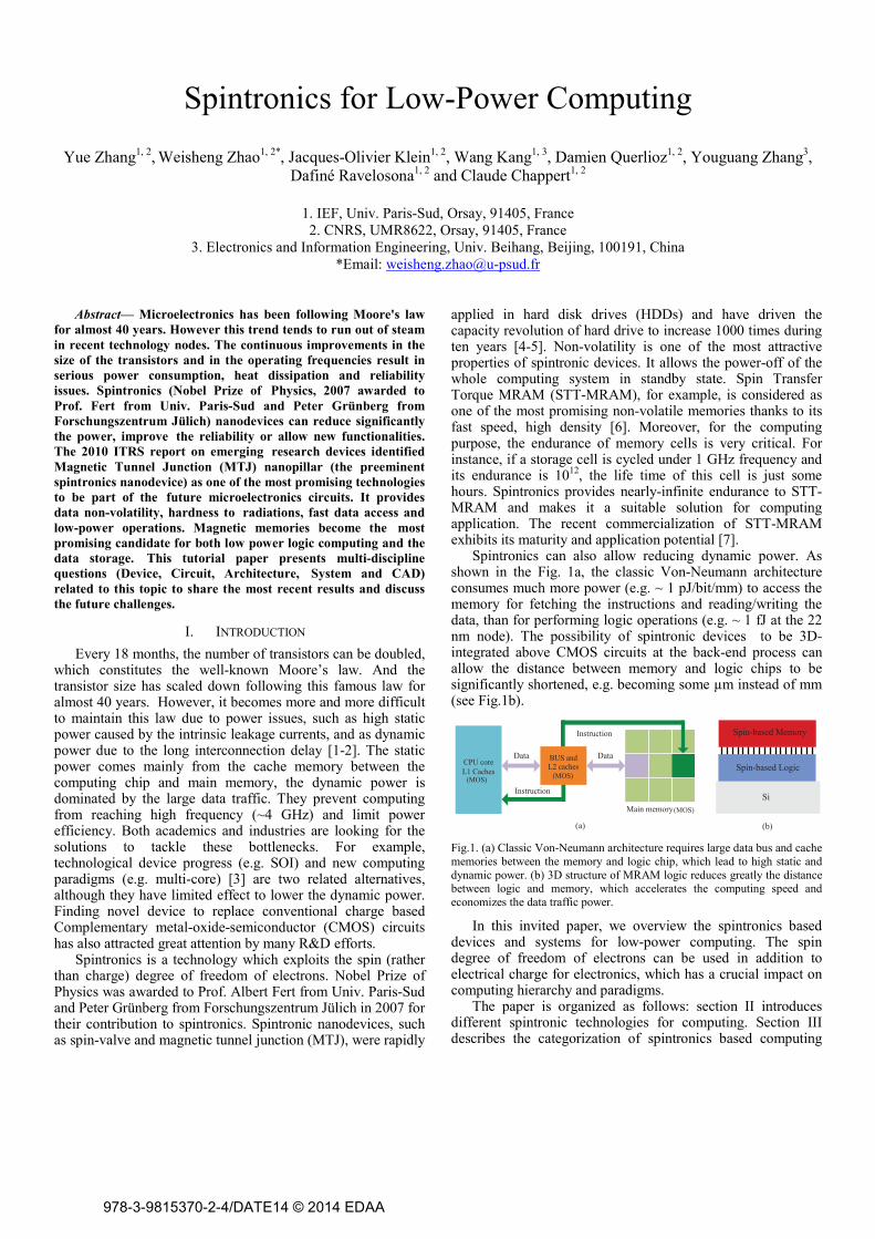
Spintronics can also allow reducing dynamic power. As shown in the Fig. 1a, the classic Von-Neumann architecture consumes much more power (e.g. ~ 1 pJ/bit/mm) to access the memory for fetching the instructions and reading/writing the data, than for performing logic operations (e.g. ~ 1 fJ at the 22 nm node). The possibility of spintronic devices to be 3D-integrated above CMOS circuits at the back-end process can allow the distance between memory and logic chips to be significantly shortened, e.g. becoming some µm instead of mm (see Fig.1b).
(MOS) (MOS)
(MOS)
Spin-based Memory
Si
Spin-based Logic
(a) (b) Fig.1. (a) Classic Von-Neumann architecture requires large data bus and cache memories between the memory and logic chip, which lead to high static and dynamic power. (b) 3D structure of MRAM logic reduces greatly the distance between logic and memory, which accelerates the computing speed and economizes the data traffic power.
In this invited paper, we overview the spintronics based devices and systems for low-power computing. The spin degree of freedom of electrons can be used in addition to electrical charge for electronics, which has a crucial impact on computing hierarchy and paradigms.
The paper is organized as follows: section II introduces different spintronic technologies for computing. Section III describes the categorization of spintronics based computing
978-3-9815370-2-4/DATE14 © 2014 EDAA
systems and logic circuits. Finally, conclusions and discussions are given.
II. DIFFERENT SPINTRONICS TECHNOLOGIES FOR COMPUTING
In this section, we classify spintronic technologies from the device point of view : MTJ nanopillar, magnetic nanowire, Spin-transistor, nanomagnet, 3D magnetic ratchet, spin wave and memristor.
A. Magnetic Tunnel Junction (MTJ) Nanopillars The magnetic tunnel junction (MTJ) nanopillar is one of the
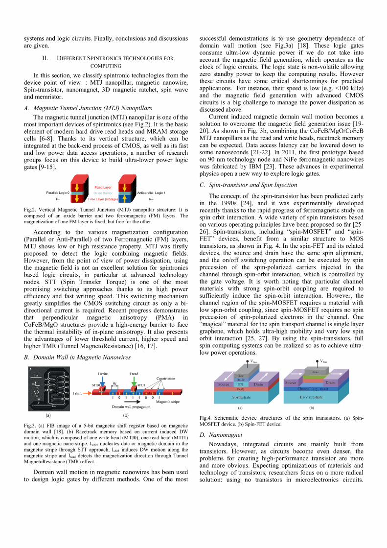
most important devices of spintronics (see Fig.2). It is the basic element of modern hard drive read heads and MRAM storage cells [6-8]. Thanks to its vertical structure, which can be integrated at the back-end process of CMOS, as well as its fast and low power data access operations, a number of research groups focus on this device to build ultra-lower power logic gates [9-15].
Fig.2. Vertical Magnetic Tunnel Junction (MTJ) nanopillar structure: It is composed of an oxide barrier and two ferromagnetic (FM) layers. The magnetization of one FM layer is fixed, but free for the other.
According to the various magnetization configuration (Parallel or Anti-Parallel) of two Ferromagnetic (FM) layers, MTJ shows low or high resistance property. MTJ was firstly proposed to detect the logic combining magnetic fields. However, from the point of view of power dissipation, using the magnetic field is not an excellent solution for spintronics based logic circuits, in particular at advanced technology nodes. STT (Spin Transfer Torque) is one of the most promising switching approaches thanks to its high power efficiency and fast writing speed. This switching mechanism greatly simplifies the CMOS switching circuit as only a bi-directional current is required. Recent progress demonstrates that perpendicular magnetic anisotropy (PMA) in CoFeB/MgO structures provide a high-energy barrier to face the thermal instability of in-plane anisotropy. It also presents the advantages of lower threshold current, higher speed and higher TMR (Tunnel MagnetoResistance) [16, 17].
B. Domain Wall in Magnetic Nanowires
(a) (b)
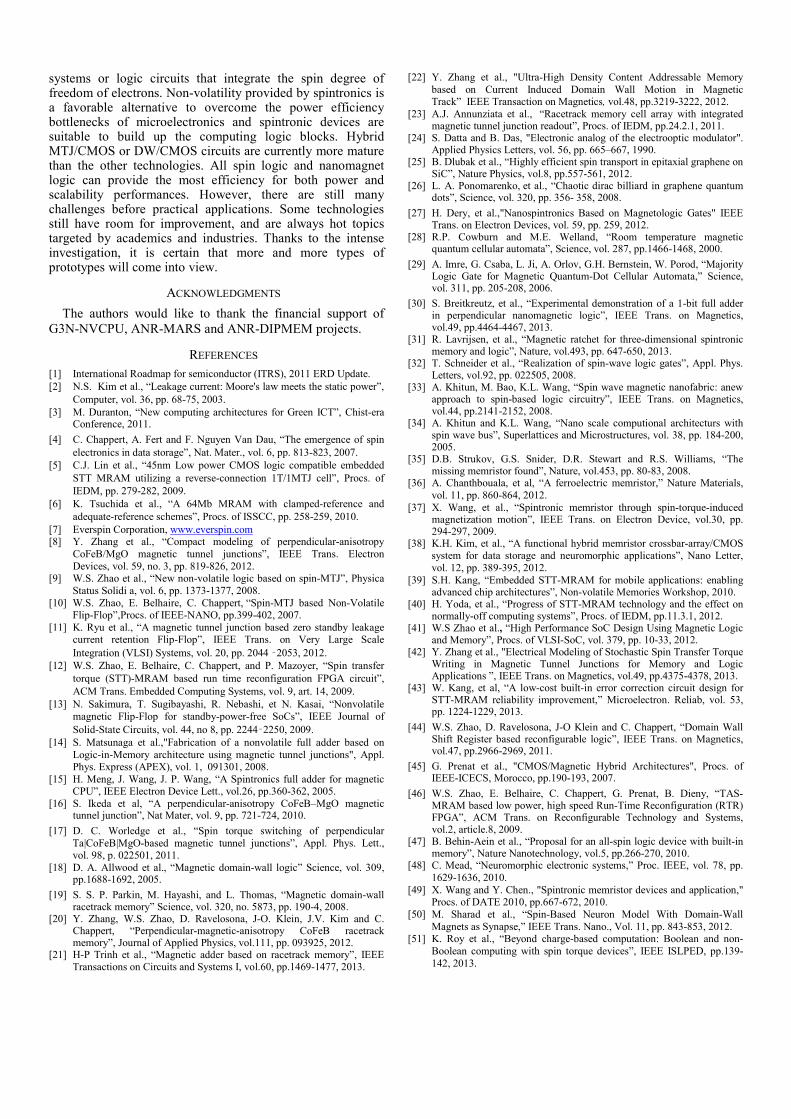
Fig.3. (a) FIB image of a 5-bit magnetic shift register based on magnetic domain wall [18]. (b) Racetrack memory based on current induced DW motion, which is composed of one write head (MTJ0), one read head (MTJ1) and one magnetic nano-stripe. Iwrite nucleates data or magnetic domain in the magnetic stripe through STT approach, Ishift induces DW motion along the magnetic stripe and Iread detects the magnetization direction through Tunnel MagnetoResistance (TMR) effect.
Domain wall motion in magnetic nanowires has been used to design logic gates by different methods. One of the most
successful demonstrations is to use geometry dependence of domain wall motion (see Fig.3a) [18]. These logic gates consume ultra-low dynamic power if we do not take into account the magnetic field generation, which operates as the clock of logic circuits. The logic state is non-volatile allowing zero standby power to keep the computing results. However these circuits have some critical shortcomings for practical applications. For instance, their speed is low (e.g. <100 kHz) and the magnetic field generation with advanced CMOS circuits is a big challenge to manage the power dissipation as discussed above.
Current induced magnetic domain wall motion becomes a solution to overcome the magnetic field generation issue [19-20]. As shown in Fig. 3b, combining the CoFeB/MgO/CoFeB MTJ nanopillars as the read and write heads, racetrack memory can be expected. Data access latency can be lowered down to some nanoseconds [21-22]. In 2011, the first prototype based on 90 nm technology node and NiFe ferromagnetic nanowires was fabricated by IBM [23]. These advances in experimental physics open a new way to explore logic gates.
C. Spin-transistor and Spin Injection
The concept of the spin-transistor has been predicted early in the 1990s [24], and it was experimentally developed recently thanks to the rapid progress of ferromagnetic study on spin orbit interaction. A wide variety of spin transistors based on various operating principles have been proposed so far [25-26]. Spin-transistors, including “spin-MOSFET” and “spin-FET” devices, benefit from a similar structure to MOS transistors, as shown in Fig. 4. In the spin-FET and its related devices, the source and drain have the same spin alignment, and the on/off switching operation can be executed by spin precession of the spin-polarized carriers injected in the channel through spin-orbit interaction, which is controlled by the gate voltage. It is worth noting that particular channel materials with strong spin-orbit coupling are required to sufficiently induce the spin-orbit interaction. However, the channel region of the spin-MOSFET requires a material with low spin-orbit coupling, since spin-MOSFET requires no spin precession of spin-polarized electrons in the channel. One “magical” material for the spin transport channel is single layer graphene, which holds ultra-high mobility and very low spin orbit interaction [25, 27]. By using the spin-transistors, full spin computing systems can be realized so as to achieve ultra-low power operations.
(a) (b) Fig.4. Schematic device structures of the spin transistors. (a) Spin-MOSFET device. (b) Spin-FET device.
D. Nanomagnet Nowadays, integrated circuits are mainly built from
transistors. However, as circuits become even denser, the problems for creating high-performance transistor are more and more obvious. Expecting optimizations of materials and technology of transistors, researchers focus on a more radical solution: using no transistors in microelectronics circuits.

Nanomagnet logic (NML) could be a potential alternative to realize computing without conventional transistors. Although the primal concepts are functional only at cryogenic temperature, Cowburn and Welland proposed a magnetic nanostructure, in which information can be propagated across a cellular automata device at room temperature in 2000 [28]. Five years later, Imre et al. reported an architecture that implemented complete logic functions [29]. Recently, the NML with PMA illustrated the great benefit of the universal majority decision. Based on the logic gates for PMA NML, such as inverter and majority gate (see Fig.5a), more complex digital logic circuit (e.g. 1-bit full adder) can be designed and fabricated (see Fig. 5b) [30].
(a) (b) Fig.5. (a) Majority gate with three input magnets: the logic operation can be realized based on the majority decision. (b) SEM image of the fabricated 1–bit full adder structure [30].
E. 3D magnetic ratchet
(a) (b)
J1
J2
J1
J2
J1
J2
J1
J2
J0
J0
Inject 1st cycle 2nd cycle 3rd cycle 4th cycle
CoFeB
Ru
Pt Ta
Si
Fig.6. (a) Schematic illustration of the experimental superlattice. (b) Soliton propagation shown by the magnetic configuration through the superlattice stack of antiferromagnetically coupled ultrathin layers [31].
Moving from mainstream 2D structure to 3D structure could allow performance enhancements, and it especially alleviates greatly the pressure to continually increase the storage density and shrink the lateral size. By accurately controlling the thickness of each magnetic layer and the exchange coupling between the layers, the 3D magnetic ratchet allows information in the form of a sharp magnetic kink soliton to be unidirectionally shifted from one magnetic layer to another [31]. As demonstrated in Fig.6, in a superlattice with numbers of layers, solitons are injected at the bottom or top. This “physical” shift register transfers data over near-atomic distances without requiring conventional transistors, and can thus execute true atomic-scale digital logic operation. Moreover, as solitons can selectively be manipulated with an external field or potentially by a spin polarized current, complex logic operation can be performed with a data shift register. This opens a route to realize 3D microchips for memory and logic computing. However, the route is still long, with many fundamental technical challenges, such as dispersion in properties, dipole fields, data
retention lifetime and the reading and writing of solitons, which should be further investigated.
F. Spin wave For spin wave logic, data is encoded in spin wave phase or
amplitude [32-33]. The process is performed by wave interference and integration with magneto-electric cells may enable non-volatile storage similar to all spin logic. The key advantage of spin wave logic (SWL) is that information transmission is accomplished without charge transfer, which can be highly beneficial for power efficiency. Moreover, it can also resolve the problem of interconnections and enhance architecture computing abilities [34]. However it consumes a lot of power for the spin wave generation, and the spin wave signal degrades rapidly during propagation. And additional power is required for data amplification. Other challenges involve CMOS compatibility, low propagation speed and device scalability.
(a) (b) Fig.7. (a) Spin-wave XNOR gate structure. (Logic ‘1’ represents a current with a phase shift of π) (b) Gate output for input shown in the diagrams [32].
G. Memristor
(a) (b) (c)
OFF
ON
R
V
Fig.8. (a) Symbol of memristor. (b) multi level switching of memristor. (c) SEM image of a crossbar array composed of memristors fabricated on top of a CMOS chip [38].
The fourth fundamental passive circuit elements (beyond the resistor, the capacitor and the inductor), called the memristor (memory+resistor) was envisioned by Leon Chua as early as 1971 as shown in Fig. 8a. It fills the gap in the set of relationships of circuit elements and covers that between the magnetic flux and the charge. However, the device was not proven experimentally until 2008 by researchers from HP-labs, and brought an upsurge for the memristors and memristive systems [35]. In an ideal memristor, when current flows in one direction through the device, the resistance increases. If the current flows in the other direction, the resistance decreases. When the current is off, the memristor retains its resistance. This is the reason why the memristor can switch among multi-level resistance states (see Fig. 8b). Although there is no uniform definition so far, the most generalized definition is that all forms of 2-terminal non-volatile memory devices based on resistance switching effects could be considered as memristor. According to that definition, many implementations have been carried out, e.g. TiO2 memristor [35], ferroelectric memristor [36], and spintronic memristor [37], etc. Based on these devices,

reconfigurable logic circuits and novel computing memory concepts attract more and more interest. One of the most promising applications is the neuromorphic system [38] (see Fig. 8c), which will be introduced in the following section.
In summary, we analyze the aforementioned spintronic technologies for different computing systems or logic circuits in Table.I. This shows that MTJ, domain wall and memristor devices currently demonstrate a broader application base.
III. LOW-POWER SPINTRONICS BASED COMPUTING ARCHITECTURES AND LOGIC CIRCUITS
Here we enumerate six spintronic computing architectures or logic circuits that achieve low-power compared with conventional CMOS architectures.
A. Normally-off computing system
(a) (b)
Generic Cell Phone
Architecture
NVSOC
DRAM NV-RAM
RFSTT-MRAM
STT Flip-Flops
STT-MRAM SPM
STT-MRAM Cache
CPU
DSPDSP
CPU
RF
Flip-Flops
SPM
Cache
Flash
Fig.9. (a) Full integration of STT-MRAM to ultra-low power computing system proposed by Qualcomm. (b) Partial integration to replace L2 or L3 cache memory and main memory proposed by Toshiba.
Normally-off computing is a novel concept with respect to the conventional “Normally-on” system, which was firstly proposed in 2010. It uses non-volatile memory to accomplish ultra-low power computing. The idea is that, when the CPU is in standby state, the information is stored in the non-volatile memories so as to achieve zero standby power. After power is reset, the data stored in the non-volatile state can be automatically recalled in the registers or flip-flop. There are already several proposals of computing system. For instance, Qualcomm proposed the full integration of STT-MRAM to build an ultra-low power computing system (see Fig. 12a) [39]; Toshiba proposed partial integration to replace only Level 2 or 3 cache memory and main memory (see Fig. 9b) by PMA
MTJ [40], since traditional SRAM and DRAM based computing hierarchy cannot reconcile fast read/write access speed, high density and low power. Spintronic devices, like MRAM, can be used for designing the normally-off system to solve the present drawbacks. For example, thanks to the fast and low-power PMA MTJ, the power consumption of cache memory in the Toshiba’s system could be reduced by over 80% compared with CMOS system without degradation of performance.
B. Logic-in-memory Logic-in-memory structure [14, 41], as shown in Fig. 10a,
which is composed of four parts: a sense amplifier (S.A) to evaluate the logic result, a non-volatile memory block (e.g., MRAM), a write circuit to program the memory, and a volatile MOS logic block. This type of spin-based logic circuits is the most popular one currently and draws considerable attention due to its good compatibility with conventional computing architectures and easy integration with the existing MOS technology process. To realize logic-in memory, many hybrid MTJ/CMOS logic circuits or prototypes have been presented in the past few years, such as magnetic flip-flop (MFF) [8], magnetic full adder (MFA) [14] and magnetic look-up table (MLUT) [12] etc. The other advantages of hybrid MTJ/CMOS logic circuits are their instant on/off capability, nearly zero standby power and hardness to power failure. However, they also suffer from some challenges which should be addressed. For example, the switching latency (several ns) of the MTJ is much larger than those of the conventional MOS logic circuits, which limits the computing frequency to the order of GHz. Another severe issue is the poor sense reliability caused mainly by the device mismatch (both MOS and MTJs devices) of the S.As and the intrinsic stochastic switching effects of the MTJs [42]. In contrast to the memory circuits where complex error correction circuits (ECCs) [43] can be employed, it is difficult to embed them in the logic circuits while keeping fast speed, low area and high power efficiency. Therefore the current efforts that concentrate on this topic are fast-access MTJ development, high-performance S.A design, low-cost and reliable integration process.
MN0
MN1, 2
MN7, 8MN5, 6
MN3, 4
Volatile
Non-volatile
Vdd
CLK
Write Circuit
C C
A
B
Input1
Input1
Input2
Input2
S.A OutOut
A A
B B
Complementary Non-volatile Spin-based memory (MRAM)
Output
Sense Amplifier (S.A)
Write Circuit
Volatile MOS Logic Tree
(a) (b) Fig.10. (a) Logic-in-memory structure; (b) An example of “XOR” gate.
C. Dynamic Reconfigurable Logic It is a challenge for the conventional logic blocks to be
dynamically or run-time reconfigurable, where they use volatile shift register to store the configuration and it takes a significant mount of time (e.g. some ms) to extract the
TABLE.I Brief Comparison of Different Spintronic Technologies for Computing
N-off
L I
M
NML
DRL
S WL
ASL
MTL
Neuro
MTJ ● ● ● ● ● Domain wall ● ● ● ●
SpinFET ● ● ● Nanomagnet ● ● 3D ratchet ● Spin wave ● ● ● Memristor ● ● ● ● *N-off: Normally-off LIM: Logic-in-memory SWL: Spin-wave logic NML: Nanomagnet logic DRL: Dynamic reconfigurable logic ASL: All spin logic MTL: Magnetic threshold logic Neuro: Neuromorphic

configuration data from the non-volatile memory out of the chip. These shortcomings of standard reconfigurable computing circuits draw the significant interest to find new memories for both the configuration and intermediate data. They should provide non-volatility to reduce standby power, fast data access (e.g. 1 ns) to ensure fast reconfiguration and computing speed (see Fig. 11a). Small cell area (e.g. < 10 F2) is also required to improve the logic density. For these purposes, a number of spintronic memories or MRAM such as STT-MRAM, magnetic domain wall based racetrack memory and thermally assisted MRAM (TAS-MRAM) are under intense investigation to be integrated in reconfigurable logic computing [13, 44-46] (see Fig. 11b). It is important to underline that MRAM-based reconfigurable computing is not mature yet. There are some other major hurdles to address beyond the low power switching technology and high reliability MTJ/CMOS hybrid circuits. For instance, we need customized system level architecture implementation tools, and good yield technological fabrication of MRAM is needed to achieve reliable data storage as there is no advanced error correction circuit embedded in the configuration memory cell.
(a) (b) Fig.11. (a) Structure of a basic reconfigurable logic gate, which is composed of a LUT and a flip-flop. (b) Micrograph of the MRAM FPGA.
D. All spin logic
(a)
(b) Fig.12. (a) All spin logic device (ASLD) with built-in memory. (b) An example of full adder layout based on ASLDs.
All spin logic devices (ASLDs) [47], as shown in Fig. 12a, employ nano-magnets as digital spin capacitors to store data information and spin currents (through STT) to communicate, realizing logic gates based on a spin majority evaluation. Fig. 12b shows an example to demonstrate the possible layouts for constructing cascadable ASLD logic gates. The magnetization directions of the nano-magnets can be switched between the stable states if enough torque is exerted on them. Information stored in the input magnet is used to generate a spin current that can be routed along a spin-coherent channel to the output magnet, determining its state based on the STT effect. The key feature of ASLD is its compactness and completeness, because
no MOS transistor is needed for the logic operations and all the logic functions can be constructed with a minimal set of Boolean logic gates. With such a design, a full spin computing system can be expected with extremely low switching power. However this is still a theoretical prospect currently and many issues, such as reliability and clock control, remain unresolved.
E. Neuromorphics Spintronics may also allow the emergence of radically
novel computing paradigms in electronics. In particular, for several years, researchers have been designing “neuromorphic” circuits that work analogously to the brain (see Fig. 13a) [48]. Such circuits could allow a form of intelligent and ultra-low power computing (the brain can solve problems inaccessible to supercomputers with only 20W). However, fabricating neuromorphic systems with pure CMOS has severe limitations, since they require massive and ideally non-volatile memory for their “synapses”. Several groups have thus proposed to use spintronic memristors as synapses [49], in particular relying on domain wall motion [50]. The associated computing units (neurons) may be realized by CMOS, but in some situations may also be implemented by multiple input spin valves. One group has shown the potential of this approach on real life applications using computer simulations [50]. An interesting point is that neuromorphic applications can tolerate more errors than traditional logic. This could allow using spintronic devices with lower currents than the other applications, which promises low power.
(a) (b) Fig.13. (a) Schematic of a neuromorphic with memristor synapses in a crossbar configuration. (b) A threshold logic gate.
F. Threshold logic The threshold logic gate (TLG) is an important element for
computing, which is widely used in microprocessors and bio-inspired information processing. The function of TLG, as shown in Fig. 13b, involves summation of weighted inputs, followed by a threshold operation given as Y=sign(∑IniWi+bi), where Ini, Wi and bi are the inputs, weights and the thresholds respectively. By using spintronic devices for realizing the inputs and weights as well as the thresholding switches, magnetic threshold logic (MTL) has been proposed [51]. For instance, the domain wall switch acts as a compact, low-power and high-speed current comparator and hence provides an energy efficient threshold operation. Compared with 4-input LUT-based CMOS FPGA, MTL shows ~97% higher energy efficiency and more than two orders of magnitude lower energy-delay product.
IV. CONCLUSION AND PERSPECTIVES In this invited paper, we presented an overview of
spintronics for low-power computing. Particularly, we addressed seven spintronic technologies and six computing
systems or logic circuits that integrate the spin degree of freedom of electrons. Non-volatility provided by spintronics is a favorable alternative to overcome the power efficiency bottlenecks of microelectronics and spintronic devices are suitable to build up the computing logic blocks. Hybrid MTJ/CMOS or DW/CMOS circuits are currently more mature than the other technologies. All spin logic and nanomagnet logic can provide the most efficiency for both power and scalability performances. However, there are still many challenges before practical applications. Some technologies still have room for improvement, and are always hot topics targeted by academics and industries. Thanks to the intense investigation, it is certain that more and more types of prototypes will come into view.
ACKNOWLEDGMENTS The authors would like to thank the financial support of
G3N-NVCPU, ANR-MARS and ANR-DIPMEM projects.
REFERENCES [1] International Roadmap for semiconductor (ITRS), 2011 ERD Update. [2] N.S. Kim et al., “Leakage current: Moore's law meets the static power”,
Computer, vol. 36, pp. 68-75, 2003. [3] M. Duranton, “New computing architectures for Green ICT”, Chist-era
Conference, 2011. [4] C. Chappert, A. Fert and F. Nguyen Van Dau, “The emergence of spin
electronics in data storage”, Nat. Mater., vol. 6, pp. 813-823, 2007. [5] C.J. Lin et al., “45nm Low power CMOS logic compatible embedded
STT MRAM utilizing a reverse-connection 1T/1MTJ cell”, Procs. of IEDM, pp. 279-282, 2009.
[6] K. Tsuchida et al., “A 64Mb MRAM with clamped-reference and adequate-reference schemes”, Procs. of ISSCC, pp. 258-259, 2010.
[7] Everspin Corporation, www.everspin.com [8] Y. Zhang et al., “Compact modeling of perpendicular-anisotropy
CoFeB/MgO magnetic tunnel junctions”, IEEE Trans. Electron Devices, vol. 59, no. 3, pp. 819-826, 2012.
[9] W.S. Zhao et al., “New non-volatile logic based on spin-MTJ”, Physica Status Solidi a, vol. 6, pp. 1373-1377, 2008.
[10] W.S. Zhao, E. Belhaire, C. Chappert, “Spin-MTJ based Non-Volatile Flip-Flop”,Procs. of IEEE-NANO, pp.399-402, 2007.
[11] K. Ryu et al., “A magnetic tunnel junction based zero standby leakage current retention Flip-Flop”, IEEE Trans. on Very Large Scale Integration (VLSI) Systems, vol. 20, pp. 2044 ‑2053, 2012.
[12] W.S. Zhao, E. Belhaire, C. Chappert, and P. Mazoyer, “Spin transfer torque (STT)-MRAM based run time reconfiguration FPGA circuit”, ACM Trans. Embedded Computing Systems, vol. 9, art. 14, 2009.
[13] N. Sakimura, T. Sugibayashi, R. Nebashi, et N. Kasai, “Nonvolatile magnetic Flip-Flop for standby-power-free SoCs”, IEEE Journal of Solid-State Circuits, vol. 44, no 8, pp. 2244‑2250, 2009.
[14] S. Matsunaga et al.,"Fabrication of a nonvolatile full adder based on Logic-in-Memory architecture using magnetic tunnel junctions", Appl. Phys. Express (APEX), vol. 1, 091301, 2008.
[15] H. Meng, J. Wang, J. P. Wang, “A Spintronics full adder for magnetic CPU”, IEEE Electron Device Lett., vol.26, pp.360-362, 2005.
[16] S. Ikeda et al, “A perpendicular-anisotropy CoFeB–MgO magnetic tunnel junction”, Nat Mater, vol. 9, pp. 721-724, 2010.
[17] D. C. Worledge et al., “Spin torque switching of perpendicular Ta|CoFeB|MgO-based magnetic tunnel junctions”, Appl. Phys. Lett., vol. 98, p. 022501, 2011.
[18] D. A. Allwood et al., “Magnetic domain-wall logic” Science, vol. 309, pp.1688-1692, 2005.
[19] S. S. P. Parkin, M. Hayashi, and L. Thomas, “Magnetic domain-wall racetrack memory” Science, vol. 320, no. 5873, pp. 190-4, 2008.
[20] Y. Zhang, W.S. Zhao, D. Ravelosona, J-O. Klein, J.V. Kim and C. Chappert, “Perpendicular-magnetic-anisotropy CoFeB racetrack memory”, Journal of Applied Physics, vol.111, pp. 093925, 2012.
[21] H-P Trinh et al., “Magnetic adder based on racetrack memory”, IEEE Transactions on Circuits and Systems I, vol.60, pp.1469-1477, 2013.
[22] Y. Zhang et al., "Ultra-High Density Content Addressable Memory based on Current Induced Domain Wall Motion in Magnetic Track” IEEE Transaction on Magnetics, vol.48, pp.3219-3222, 2012.
[23] A.J. Annunziata et al., “Racetrack memory cell array with integrated magnetic tunnel junction readout”, Procs. of IEDM, pp.24.2.1, 2011.
[24] S. Datta and B. Das, "Electronic analog of the electrooptic modulator". Applied Physics Letters, vol. 56, pp. 665–667, 1990.
[25] B. Dlubak et al., “Highly efficient spin transport in epitaxial graphene on SiC”, Nature Physics, vol.8, pp.557-561, 2012.
[26] L. A. Ponomarenko, et al., “Chaotic dirac billiard in graphene quantum dots”, Science, vol. 320, pp. 356- 358, 2008.
[27] H. Dery, et al.,"Nanospintronics Based on Magnetologic Gates" IEEE Trans. on Electron Devices, vol. 59, pp. 259, 2012.
[28] R.P. Cowburn and M.E. Welland, “Room temperature magnetic quantum cellular automata”, Science, vol. 287, pp.1466-1468, 2000.
[29] A. Imre, G. Csaba, L. Ji, A. Orlov, G.H. Bernstein, W. Porod, “Majority Logic Gate for Magnetic Quantum-Dot Cellular Automata,” Science, vol. 311, pp. 205-208, 2006.
[30] S. Breitkreutz, et al., “Experimental demonstration of a 1-bit full adder in perpendicular nanomagnetic logic”, IEEE Trans. on Magnetics, vol.49, pp.4464-4467, 2013.
[31] R. Lavrijsen, et al., “Magnetic ratchet for three-dimensional spintronic memory and logic”, Nature, vol.493, pp. 647-650, 2013.
[32] T. Schneider et al., “Realization of spin-wave logic gates”, Appl. Phys. Letters, vol.92, pp. 022505, 2008.
[33] A. Khitun, M. Bao, K.L. Wang, “Spin wave magnetic nanofabric: anew approach to spin-based logic circuitry”, IEEE Trans. on Magnetics, vol.44, pp.2141-2152, 2008.
[34] A. Khitun and K.L. Wang, “Nano scale computional architecturs with spin wave bus”, Superlattices and Microstructures, vol. 38, pp. 184-200, 2005.
[35] D.B. Strukov, G.S. Snider, D.R. Stewart and R.S. Williams, “The missing memristor found”, Nature, vol.453, pp. 80-83, 2008.
[36] A. Chanthbouala, et al, “A ferroelectric memristor,” Nature Materials, vol. 11, pp. 860-864, 2012.
[37] X. Wang, et al., “Spintronic memristor through spin-torque-induced magnetization motion”, IEEE Trans. on Electron Device, vol.30, pp. 294-297, 2009.
[38] K.H. Kim, et al., “A functional hybrid memristor crossbar-array/CMOS system for data storage and neuromorphic applications”, Nano Letter, vol. 12, pp. 389-395, 2012.
[39] S.H. Kang, “Embedded STT-MRAM for mobile applications: enabling advanced chip architectures”, Non-volatile Memories Workshop, 2010.
[40] H. Yoda, et al., “Progress of STT-MRAM technology and the effect on normally-off computing systems”, Procs. of IEDM, pp.11.3.1, 2012.
[41] W.S Zhao et al., “High Performance SoC Design Using Magnetic Logic and Memory”, Procs. of VLSI-SoC, vol. 379, pp. 10-33, 2012.
[42] Y. Zhang et al., "Electrical Modeling of Stochastic Spin Transfer Torque Writing in Magnetic Tunnel Junctions for Memory and Logic Applications ”, IEEE Trans. on Magnetics, vol.49, pp.4375-4378, 2013.
[43] W. Kang, et al, “A low-cost built-in error correction circuit design for STT-MRAM reliability improvement,” Microelectron. Reliab, vol. 53, pp. 1224-1229, 2013.
[44] W.S. Zhao, D. Ravelosona, J-O Klein and C. Chappert, “Domain Wall Shift Register based reconfigurable logic”, IEEE Trans. on Magnetics, vol.47, pp.2966-2969, 2011.
[45] G. Prenat et al., "CMOS/Magnetic Hybrid Architectures", Procs. of IEEE-ICECS, Morocco, pp.190-193, 2007.
[46] W.S. Zhao, E. Belhaire, C. Chappert, G. Prenat, B. Dieny, “TAS-MRAM based low power, high speed Run-Time Reconfiguration (RTR) FPGA”, ACM Trans. on Reconfigurable Technology and Systems, vol.2, article.8, 2009.
[47] B. Behin-Aein et al., “Proposal for an all-spin logic device with built-in memory”, Nature Nanotechnology, vol.5, pp.266-270, 2010.
[48] C. Mead, “Neuromorphic electronic systems,” Proc. IEEE, vol. 78, pp. 1629-1636, 2010.
[49] X. Wang and Y. Chen., "Spintronic memristor devices and application," Procs. of DATE 2010, pp.667-672, 2010.
[50] M. Sharad et al., “Spin-Based Neuron Model With Domain-Wall Magnets as Synapse,” IEEE Trans. Nano., Vol. 11, pp. 843-853, 2012.
[51] K. Roy et al., “Beyond charge-based computation: Boolean and non-Boolean computing with spin torque devices”, IEEE ISLPED, pp.139-142, 2013.