spps-27-48f-n2-idfb - source photonics...spps-27-48f-n2-idfb ds-8145 rev 00 2017-04-09 features...
TRANSCRIPT
SPPS-27-48F-N2-IDFB
DS-8145 Rev 00 2017-04-09
Features
Single fiber bi-directional data links with asymmetric
2.48832 Gbps upstream and 9.95328 Gbps
downstream
Sleep Mode for Power Consumption
1270nm burst mode transmitter with DFB Laser
1577nm continuous mode receiver with APD
Compliant with ITU-TG.987.2 XG-GPON N2 class
SFP+ MSA SFF-8431 Compliant
Digital diagnostic SFF-8472 Rev9.5 Compliant
Telcordia GR-468 compliant
Single 3.3V power supply
Operation case temperature:-40-85°C
SFP+ (Small Form-factor Pluggable Plus) package
with SC receptacle optical interface.
RoHS Compliant
Regulatory Compliance
Table 1 - Regulatory Compliance
Feature Standard Performance
Electrostatic Discharge
(ESD) to the Electrical Pins
MIL-STD-883E
Method 3015.7 Class 1(>500 V)
Electrostatic Discharge (ESD) to the
Duplex LC Receptacle IEC 61000-4-2 Compatible with standards
Electromagnetic
Interference (EMI)
FCC Part 15 Class B
EN55022 Class B (CISPR 22B) Compatible with standards
Immunity IEC 61000-4-3 Compatible with standards
Laser Eye Safety FDA 21CFR 1040.10 and 1040.11
EN60950, EN (IEC) 60825-1,2
Compatible with Class I laser
product.
Component Recognition UL and CSA Compliant with standards
RoHS 2011/65/EU Compliant with standards note
Note:
In light of item 5 in Annex of 2011/65/EU, “Pb in the glass of cathode ray tubes, electronic components and
fluorescent tubes.” and item 13 in Annex of 2005/747/EC, “Lead and cadmium in optical and filter glass.”, the
two exemptions are being concerned for Source Photonics transceivers, because Source Photonics
transceivers use glass, which may contain Pb, for components such as lenses, windows, isolators, and other
electronic components.

SPPS-27-48F-N2-IDFB
DS-8145 Rev 00 2017-04-09
Absolute Maximum Ratings
Table 2 - Absolute Maximum Ratings
Parameter Symbol Min. Typical Max. Unit Notes
Storage Ambient Temperature TS -40 - 85 °C
Operating Case Temperature TC -40 85 °C 1
Operating Relative Humidity RH 5 95 %
Power Supply Voltage VCC 0 4 V
Note 1: When ambient temperature is above 60°C, airflow at rate higher than 1m/sec is required.
Recommended Operating Conditions
Table 3 – Recommended Operating Conditions
Parameter Symbol Min. Typical Max. Unit Notes
Power Supply Voltage VCC 3.13 3.3 3.47 V
Operating Case Temperature TC -40 85 °C 1
Operating Relative Humidity RH 5 95 %
Data Rate DR 2.48832 Gbit/s 2
Data Rate Drift -100 +100 PPM
Note 1: When ambient temperature is above 60°C, airflow at rate higher than 1m/sec is required.
2: PRBS223-1.
Optical Characteristics
Table 4 – Optical Characteristics
Transmitter
Parameter Symbol Min. Typical Max. Unit Notes
Centre Wavelength λC 1260 1280 nm
Spectral Width (-20dB) ∆λ 1 nm
Side Mode Suppression Ratio SMSR 30 dB
Average Launch Power POUT 2 7 dBm 1
Average Launch Power-OFF
Transmitter
POFF -43.5 dBm
Extinction Ratio EX 8.2 dB 2
Total Jitter TJ 0.2 UI 2
Rise/Fall Time (20%-80%) TR/TF 140 ps 2,3
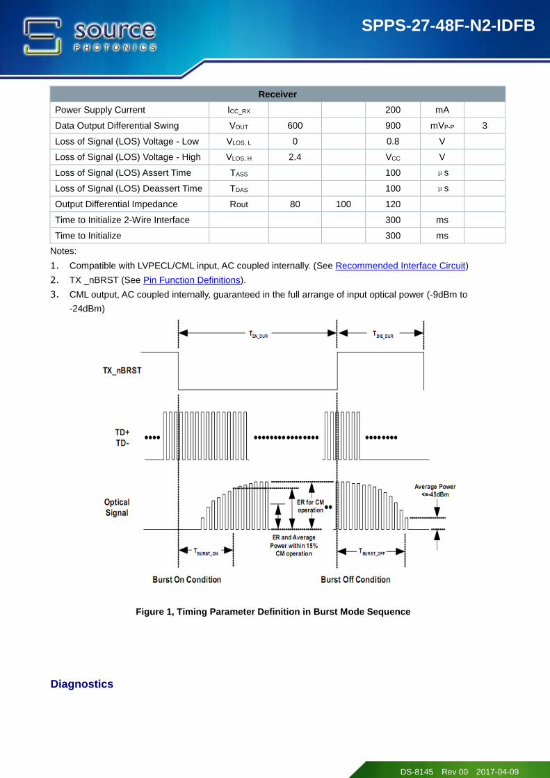
Burst Turn On Time TBURST_ON 32 ns 4
Burst Turn Off Time TBURST_OFF 32 ns 4
Optical Return Loss Tolerance -15 dB

SPPS-27-48F-N2-IDFB
DS-8145 Rev 00 2017-04-09
Transmitter Reflectance -6 dB
Optical Eye Mask Compliant With ITU-T G.987.2
Receiver
Operating Wavelength λC 1575 1577 1580 nm
Sensitivity PSEN -28 dBm 5
Saturation PSAT -8 dBm
Receiver Total Jitter TJ - - 0.7 UI
Receiver Deterministic Jitter DJ - - 0.42 UI
SD-Assert PSDA -30 dBm
SD-Deassert PSDD -39 - dBm
Receiver Reflectance(6) -30 dB
WDM Filter Isolation ISO(1550) 38 dB 1550nm
ISO(1650) 35 dB 1650nm
Notes:
1. The optical power is launched into 9/125um SMF.
2. Measured with PRBS 223-1 test pattern @2.48832Gbps.
3. Measured with the Bessel-Thompson filter OFF.
4. Refer to Timing Parameter Definition in Burst Mode Sequence
5. PSEN1 measured with a PRBS223-1 test [email protected],BER≦10-10 for reference
PSEN2 measured with a PRBS223-1 test pattern @9.95328Gbps, BER≦10-3
6. From external 1260-1280nm to 1575-1581nm
Electrical Characteristics
Table 5 – Electrical Characteristics
Transmitter
Parameter Symbol Min. Typical Max. Unit Notes
Power Supply Current ICC_TX 250 mA
Data Input Differential Swing VIN 200 1600 mVp-p 1
Input Differential Impedance ZIN 90 100 110 Ω
Transmitter Disable Voltage - Low VTDIS, L 0 0.8 V 2
Transmitter Disable Voltage - High VTDIS, H 2.0 Vcc V
Transmitter Fault Assert Time T-FAULT-ON 0 0.4 V
Transmitter Fault Reset TX_Fault Reset 2.4 Vcc V
Power Down Voltage _Low V_PDL 0 0.8
Power Down Voltage _High V_PDH 2.0 VCC
TX Power Down Assert Time T_PD assert 512 ns
Recovery Time following TX Power Down
following TX Sleep
T_PD recover 512 ns
SPPS-27-48F-N2-IDFB
DS-8145 Rev 00 2017-04-09
Receiver
Power Supply Current ICC_RX 200 mA
Data Output Differential Swing VOUT 600 900 mVP-P 3
Loss of Signal (LOS) Voltage - Low VLOS, L 0 0.8 V
Loss of Signal (LOS) Voltage - High VLOS, H 2.4 VCC V
Loss of Signal (LOS) Assert Time TASS 100 μs
Loss of Signal (LOS) Deassert Time TDAS 100 μs
Output Differential Impedance Rout 80 100 120
Time to Initialize 2-Wire Interface 300 ms
Time to Initialize 300 ms
Notes:
1. Compatible with LVPECL/CML input, AC coupled internally. (See Recommended Interface Circuit)
2. TX _nBRST (See Pin Function Definitions).
3. CML output, AC coupled internally, guaranteed in the full arrange of input optical power (-9dBm to
-24dBm)
Figure 1, Timing Parameter Definition in Burst Mode Sequence
Diagnostics

SPPS-27-48F-N2-IDFB
DS-8145 Rev 00 2017-04-09
Table 6 – Diagnostics
Parameter Range Accuracy Unit Calibration
Temperature -45 to 90 ±3 ºC Internal
Voltage 0 to Vcc ±3% V Internal
Bias Current 0 to 90(notes) ±10% mA Internal
Tx Power 2 to 7 ±3 dB Internal
Rx Power -30 to -8 ±2 dB Internal
Notes: only for continuous mode
Table 7 – EEPROM Serial ID (A0h)
Addr. Field Size (Bytes) Name of Field Hex Description
0 1 Identifier 03 SFP+ transceiver
1 1 Ext. Identifier 04 MOD4
2 1 Connector 01 SC
3-10 8 Transceiver 00 10 00 00 00 00 00 00 OC48
11 1 Encoding 03 NRZ
12 1 BR, Nominal 19 2.48832Gbps
13 1 Reserved 00
14 1 Length (9um)-km 14 20(km)
15 1 Length (9um) C8 200(100m)
16 1 Length (50um) 00 Not Support MMF
17 1 Length (62.5um) 00 Not Support MMF
18 1 Length (Copper) 00 Not Support Copper
19 1 Reserved 00
20-35 16 Vendor name 53 4F 55 52 43 45 50 48
4F 54 4F 4E 49 43 53 20
“SOURCEPHOTONICS ”(ASC
Ⅱ)
36 1 Reserved 00
37-39 3 Vendor OUI 00 1F 22 SP vendor OUI
40-55 16 Vendor PN 53 50 50 53 32 37 34 38
46 4E 32 49 44 46 42 20 “SPPS2748FN2IDFB (ASCII)
56-59 4 Vendor Rev X X 20 20 ASCII(“31 30 20 20” means 1.0
Revision)
60-61 2 Wavelength 04 F6 1270nm Laser Wavelength
62 1 Reserved 00
63 1 CC_BASE xx Check sum of byte 0-62
64-65 2 Options 00 0A LOS,TX_FAULT
66 1 BR, max 00
67 1 BR, min 00
68-83 16 Vendor SN xx xx xx xx xx xx xx xx
xx xx xx xx xx xx xx xx ASCII
SPPS-27-48F-N2-IDFB
DS-8145 Rev 00 2017-04-09
84-91 8 Date code xx xx xx xx xx xx 20 20 Year(2bytes),Month(2bytes),
Day(2 bytes)
92 1 Diagnostic
Monitoring Type 68
Compliant with SFF-8472 V9.5
Externally Calibrated
Received power measurement type
-Average Power
93 1 Enhanced
Options F0
Diagnostics (Optional
Alarm/warning flags)
Soft TX_FAULT monitoring
implemented
Soft TX_Disable monitoring
implemented
Soft RX_LOS monitoring
implemented
94 1 SFF-8472
Compliance 02
Diagnostics
Compliance(SFF-8472 V9.5)
95 1 CC_EXT Check sum of byte 64-94
96-255 64 Vendor Specific
Table 8– Pin Definitions
Pin Symbol Name/Description
1 VeeT Module Transmitter Ground (note1)
2 TX_FAULT Module Transmitter Fault
3 TX_nBRST Transmitter Burst Control (note2)
4 SDL 2-Wire Serial Interface Data Line (MOD-DEF2) (note3)
5 SCL 2-Wire Serial Interface Clock (MOD-DEF1)
6 MOD_ABS Module Absent, connected to VeeT or VeeR in the module
7 Tx_SD Tx Signal Detect (note4)
8 RX_LOS Receiver Loss of Signal Indication (in FC designated as RX_LOS, in SONET
designated as LOS, and in Ethernet designated as NOT Signal Detect)
9 PDWN_TX Power saving of Tx side, On/off time less than 1ms, high active, if not use this feature, main
board connection should be NC.(Note5)
10 VeeR Module Receiver Ground
11 VeeR Module Receiver Ground
12 RXD- Receiver Inverted Data Output
13 RXD+ Receiver Non-Inverted Data Output
14 VeeR Module Receiver Ground
15 VCCR Module Receiver 3.3V Supply
16 VCCT Module Transmitter 3.3V Supply
17 VeeT Module Transmitter Ground
18 TXD+ Transmitter Non-Inverted Data Input

SPPS-27-48F-N2-IDFB
DS-8145 Rev 00 2017-04-09
19 TXD- Transmitter Inverted Data Input
20 VeeT Module Transmitter Ground
Note
1. The module ground pins, VeeR and VeeT, shall be isolated from the module case.
2. Tx_nburst is an input that is used to shut down the transmitter optical output.
3. MOD-DEF0,1,2. These are the module definition pins. They should be pulled up with a 4.7K-10KΩ resistor
on the host board. The pull-up voltage shall be VccT or VccR.
4. Tx Signal Detect, Tx Active State: High.
5. Tx Power saving function timing: Tx_Sleep
SFP+ Module PCB Pinout
Recommended Host Board Power Supply Circuit
TX_Burst
TX_Sleep
TX_Burst_Off
TX_Sleep_On
1ms 1ms

SPPS-27-48F-N2-IDFB
DS-8145 Rev 00 2017-04-09
Recommended Interface Circuit
Figure 2, Recommended Interface Circuit
Mechanical Diagram

SPPS-27-48F-N2-IDFB
DS-8145 Rev 00 2017-04-09
Figure 3, Mechanical Diagram
Order Information
Table9 – Order Information
Part No. Application Data Rate Laser Source Fiber
Type
SPPS-27-48F-N2-IDFB XGPON N1/N2 Class
ONT
Tx 2.48832Gb/s and
Rx 9.95328Gb/s
asymmetric
1270nm DFB SMF
SPPS-27-48F-N2-IDFB
DS-8145 Rev 00 2017-04-09
Warnings
Handling Precautions: This device is susceptible to damage as a result of electrostatic discharge (ESD). A
static free environment is highly recommended. Follow guidelines according to proper ESD procedures.
Laser Safety: Radiation emitted by laser devices can be dangerous to human eyes. Avoid eye exposure to
direct or indirect radiation.
Legal Notice
IMPORTANT NOTICE!
All information contained in this document is subject to change without notice, at Source Photonics’ sole and
absolute discretion. Source Photonics warrants performance of its products to current specifications only in
accordance with the company’s standard one-year warranty; however, specifications designated as
“preliminary” are given to describe components only, and Source Photonics expressly disclaims any and all
warranties for said products, including express, implied, and statutory warranties, warranties of
merchantability, fitness for a particular purpose, and non-infringement of proprietary rights. Please refer to the
company’s Terms and Conditions of Sale for further warranty information.
Source Photonics assumes no liability for applications assistance, customer product design, software
performance, or infringement of patents, services, or intellectual property described herein. No license, either
express or implied, is granted under any patent right, copyright, or intellectual property right, and Source
Photonics makes no representations or warranties that the product(s) described herein are free from patent,
copyright, or intellectual property rights. Products described in this document are NOT intended for use in
implantation or other life support applications where malfunction may result in injury or death to persons.
Source Photonics customers using or selling products for use in such applications do so at their own risk and
agree to fully defend and indemnify Source Photonics for any damages resulting from such use or sale.
THE INFORMATION CONTAINED IN THIS DOCUMENT IS PROVIDED ON AN “AS IS” BASIS. Customer
agrees that Source Photonics is not liable for any actual, consequential, exemplary, or other damages arising
directly or indirectly from any use of the information contained in this document. Customer must contact
Source Photonics to obtain the latest version of this publication to verify, before placing any order, that the
information contained herein is current.
Contact
U.S.A. Headquarters
8521 Fallbrook Avenue
Suite 200, West Hills,CA
91304,USA
Tel: +1-818-773-9044
Fax: +1-818-773-0261
China
Building #2&5, West Export Processing Zone
No. 8 Kexin Road, Hi-Tech Zone
Chengdu, 611731, China
Tel: +86-28-8795-8788
Fax: +86-28-8795-8789
Taiwan
9F, No 81, Shui Lee Rd.
Hsinchu, 300, Taiwan
R.O.C.
Tel: +886-3-5169222
Fax: +886-3-5169213
© Copyright Source Photonics, Inc.
All rights reserved