spring 2006 1 ee 437 lillevik 437s06-l2 university of portland school of engineering advanced...
TRANSCRIPT

Spring 2006
Lillevik 437s06-l2 1University of Portland School of Engineering
EE 437
Advanced ComputerArchitecture
Lecture 2
NSD with MUX and ROM
Class CPU model

Spring 2006
Lillevik 437s06-l2 2University of Portland School of Engineering
EE 437
FSM design
• Assume: synchronous solution
• Describe: what your design should do
• Determine: inputs and outputs
• Create: state diagram
• Assign: adjacent states (no glitches)
• Prepare: next state table
• Explore: implementation options

Spring 2006
Lillevik 437s06-l2 3University of Portland School of Engineering
EE 437
FSM architecture
Present
State
NS
Decoder
Output
Decoder
Inputs Outputs
Combo logic
ROM
MUX
Combo logic
ROM
MUX
Decoder
Flip Flops

Spring 2006
Lillevik 437s06-l2 4University of Portland School of Engineering
EE 437
Example design
Design a 2-bit, Grey code counter with two control signals: enable, up/downSequence = {0, 1, 3, 2, 0}
NOTE: no output decoder required

Spring 2006
Lillevik 437s06-l2 5University of Portland School of Engineering
EE 437
Prepare next state tableInputs
Present State
Next State
Outputs
U/D Enable Q1 Q0
0
0
1
1
0
1
0
1
00
00
00
00
00
10
00
01
0
1
0
0
0
0
0
1
0
0
1
1
0
1
0
1
01
01
01
01
01
00
01
11
0
0
0
1
1
0
1
1
0
0
1
1
0
1
0
1
10
10
10
10
10
11
10
00
1
1
1
0
0
1
0
0
0
0
1
1
0
1
0
1
11
11
11
11
11
01
11
10
1
0
1
1
1
1
1
0
Cou
nt U
p
Spring 2006
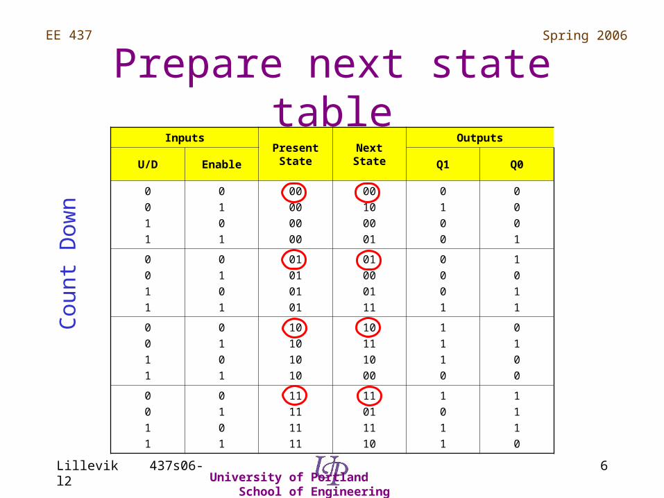
Lillevik 437s06-l2 6University of Portland School of Engineering
EE 437
Prepare next state tableInputs
Present State
Next State
Outputs
U/D Enable Q1 Q0
0
0
1
1
0
1
0
1
00
00
00
00
00
10
00
01
0
1
0
0
0
0
0
1
0
0
1
1
0
1
0
1
01
01
01
01
01
00
01
11
0
0
0
1
1
0
1
1
0
0
1
1
0
1
0
1
10
10
10
10
10
11
10
00
1
1
1
0
0
1
0
0
0
0
1
1
0
1
0
1
11
11
11
11
11
01
11
10
1
0
1
1
1
1
1
0
Cou
nt D
own
Spring 2006
Lillevik 437s06-l2 7University of Portland School of Engineering
EE 437
Next state decoder examples
• Sum of products (SOP)
• MUX
• ROM

Spring 2006
Lillevik 437s06-l2 8University of Portland School of Engineering
EE 437
NSD SOP Implementation
• Two decoders determine the 16 NSD states
• An OR gate combines all the K-map cells with a 1– D0 = {1,3,6,7,9,b,c,d}
– D1 = {2,3,4,6,a,b,d,f}

Spring 2006
Lillevik 437s06-l2 9University of Portland School of Engineering
EE 437
Schematic
0 - 7
8 - f
Or gates
SOP Implementation
NSD

Spring 2006
Lillevik 437s06-l2 10University of Portland School of Engineering
EE 437
NSD MUX implementation
• Reduce next state table– For each present state, do K-map on remaining
inputs– Reduced K-map contains logic expression
• Implementation– Connect present state to MUX select lines– Enter logic function on each input
Spring 2006
Lillevik 437s06-l2 11University of Portland School of Engineering
EE 437
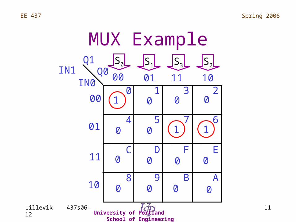
MUX Example
0 1 3 2
4 5 7 6
8 9 B A
C D F E
Q1Q0IN1
IN000 01 11 10
00
01
11
10
1
1 1
0 0 0
00
0 0 0 0
0 0 0 0
S0 S1 S3 S2

Spring 2006
Lillevik 437s06-l2 12University of Portland School of Engineering
EE 437
MUX Implementation
0 1
2 3
Q0
Q1
0IN1·IN0
IN1·IN0 IN1·IN0
S
0
1
2
3
Din
Q1,Q0
IN1·IN0
Gnd
IN1·IN0
IN1·IN0
LS153
2
Spring 2006
Lillevik 437s06-l2 13University of Portland School of Engineering
EE 437
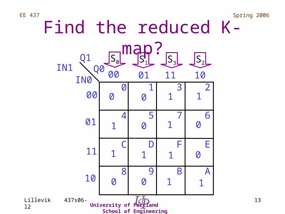
Find the reduced K-map?
0 1 3 2
4 5 7 6
8 9 B A
C D F E
Q1Q0IN1
IN000 01 11 10
00
01
11
10
0
1 0
0 1 1
01
1 1 1 0
0 0 1 1
S0 S1 S3 S2

Spring 2006
Lillevik 437s06-l2 14University of Portland School of Engineering
EE 437
Find the Implementation?
0 1
2 3
Q0
Q1
S
0
1
2
3
Din
Q1,Q0
LS153
2
Spring 2006
Lillevik 437s06-l2 15University of Portland School of Engineering
EE 437
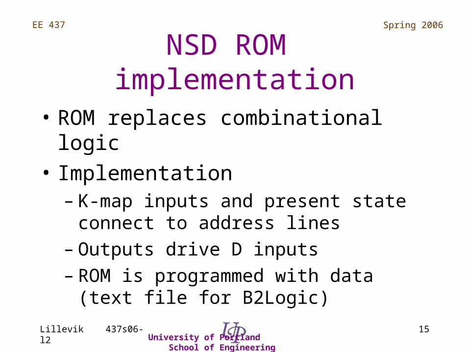
NSD ROM implementation
• ROM replaces combinational logic
• Implementation– K-map inputs and present state connect to
address lines– Outputs drive D inputs– ROM is programmed with data (text file for
B2Logic)

Spring 2006
Lillevik 437s06-l2 16University of Portland School of Engineering
EE 437
ROM Example
0 1 3 2
4 5 7 6
8 9 B A
C D F E
Q1Q0
IN1IN0
00 01 11 10
00
01
11
10
1
1 1
0 0 0
00
0 0 0 0
0 0 0 0

Spring 2006
Lillevik 437s06-l2 17University of Portland School of Engineering
EE 437
ROM Implementation
16 x 1 ROM
A0
A1
A2
A3
D0
Q0
Q1
IN0
IN1D0
Connect present state to upper address lines

Spring 2006
Lillevik 437s06-l2 18University of Portland School of Engineering
EE 437
ROM text file
Address Data
0 1
7 1
6 1
NOTE: ROM text files default to zero
Spring 2006
Lillevik 437s06-l2 19University of Portland School of Engineering
EE 437
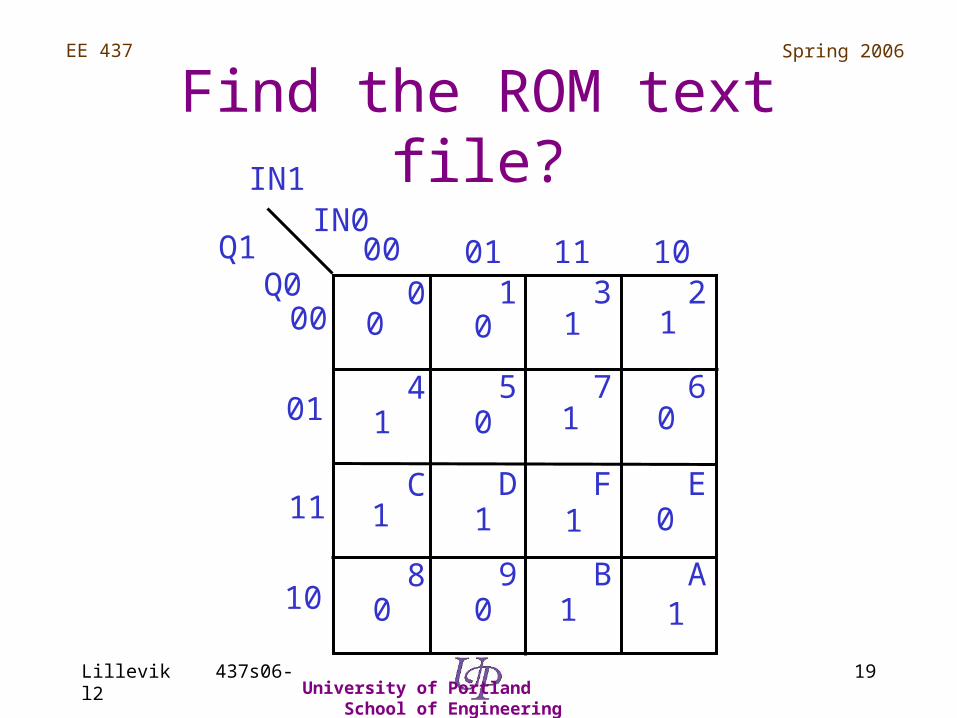
Find the ROM text file?
0 1 3 2
4 5 7 6
8 9 B A
C D F E
Q1Q0
IN1IN0
00 01 11 10
00
01
11
10
0
1 0
0 1 1
01
1 1 1 0
0 0 1 1
Spring 2006
Lillevik 437s06-l2 20University of Portland School of Engineering
EE 437
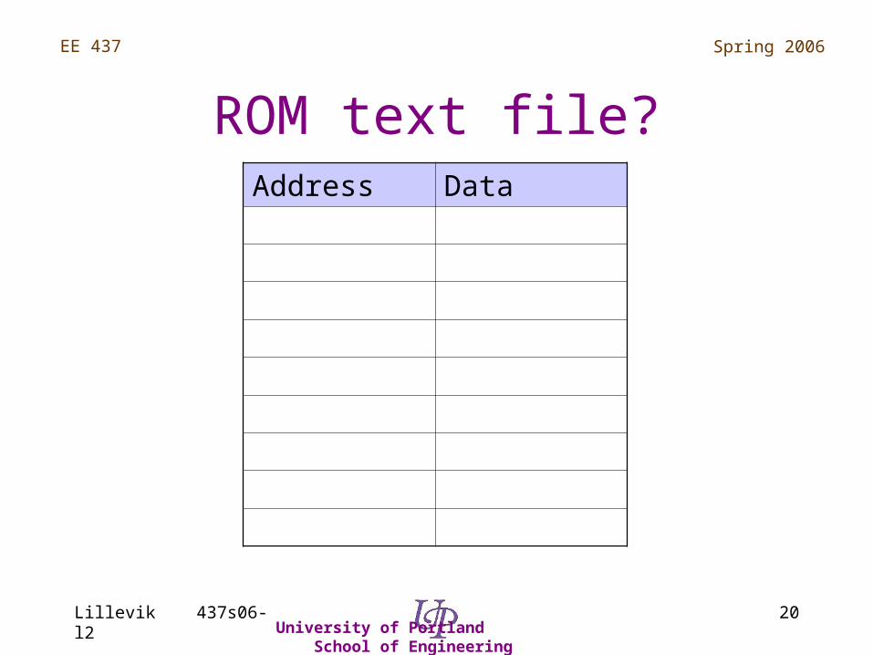
ROM text file?Address Data

Spring 2006
Lillevik 437s06-l2 21University of Portland School of Engineering
EE 437
What is a bus?
···
Signal 0
Signal n
Agent 0 Agent n···
Bus
Bus: collection of n parallel signals

Spring 2006
Lillevik 437s06-l2 22University of Portland School of Engineering
EE 437
Example Buses?
• USB
• PCI, PCI-E
• AGP
• ISA, EISA
• ATA, SATA
• SCSI
• MULTIBUS, VERSABUS, DECBUS

Spring 2006
Lillevik 437s06-l2 23University of Portland School of Engineering
EE 437
Bus properties
• Agents– Master: owns bus– Slave: responds to requests
• Interconnections– Parallel, serial– Point-to-point, distributed– Single- and multi-master

Spring 2006
Lillevik 437s06-l2 24University of Portland School of Engineering
EE 437
Bus properties, continued.
• Electrical– Synchronous, asynchronous– Logic families: setup, hold, propagation– Impedance, length, speed
• Performance– Bandwidth, B/s– Turn-around time, t
Spring 2006
Lillevik 437s06-l2 25University of Portland School of Engineering
EE 437
Bus signal groups
• Address– Identifies memory location– Identifies I/O port number
• Data– Contains information– Uni- or Bi-directional (tri-state)
• Control: coordinates actions
Spring 2006
Lillevik 437s06-l2 26University of Portland School of Engineering
EE 437
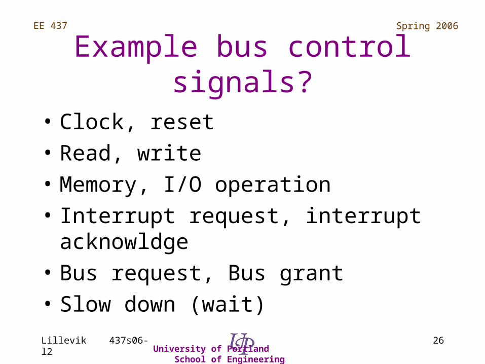
Example bus control signals?
• Clock, reset
• Read, write
• Memory, I/O operation
• Interrupt request, interrupt acknowldge
• Bus request, Bus grant
• Slow down (wait)

Spring 2006
Lillevik 437s06-l2 27University of Portland School of Engineering
EE 437
Bus cycle (phases)
1. Arbitration: owner defined
2. Address: ID of memory or I/O provided
3. Data: information transferred
4. Response: indicates completion of cycle
Spring 2006
Lillevik 437s06-l2 28University of Portland School of Engineering
EE 437
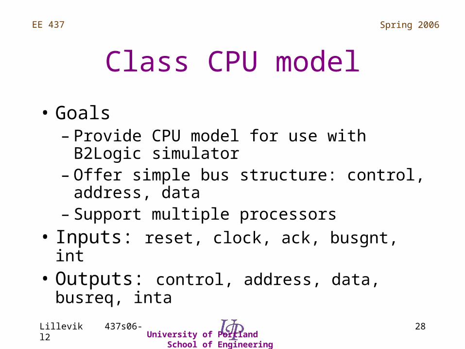
Class CPU model
• Goals– Provide CPU model for use with B2Logic
simulator– Offer simple bus structure: control, address,
data– Support multiple processors
• Inputs: reset, clock, ack, busgnt, int
• Outputs: control, address, data, busreq, inta

Spring 2006
Lillevik 437s06-l2 29University of Portland School of Engineering
EE 437
CPU functional diagram
CPU
Model
Reset/
Clk
Ack
BusgntInt
C
A
D
BusreqInta

Spring 2006
Lillevik 437s06-l2 30University of Portland School of Engineering
EE 437
Inputs
• Reset/ Places CPU in known state
• Clk Clock for synchronous logic
• Ack Indicates bus cycle complete
• Busgnt Bus granted to CPU
• Int Interrupt request

Spring 2006
Lillevik 437s06-l2 31University of Portland School of Engineering
EE 437
Outputs
• A Address of bus operation (8 bits)
• D Data for bus operation, it is abi-directional bus (8 bits)
• C Control bits indicate type of bus operation (4 bits)
• Busreq CPU requests use of bus
• Inta CPU acknowledges an interrupt input
Spring 2006
Lillevik 437s06-l2 32University of Portland School of Engineering
EE 437
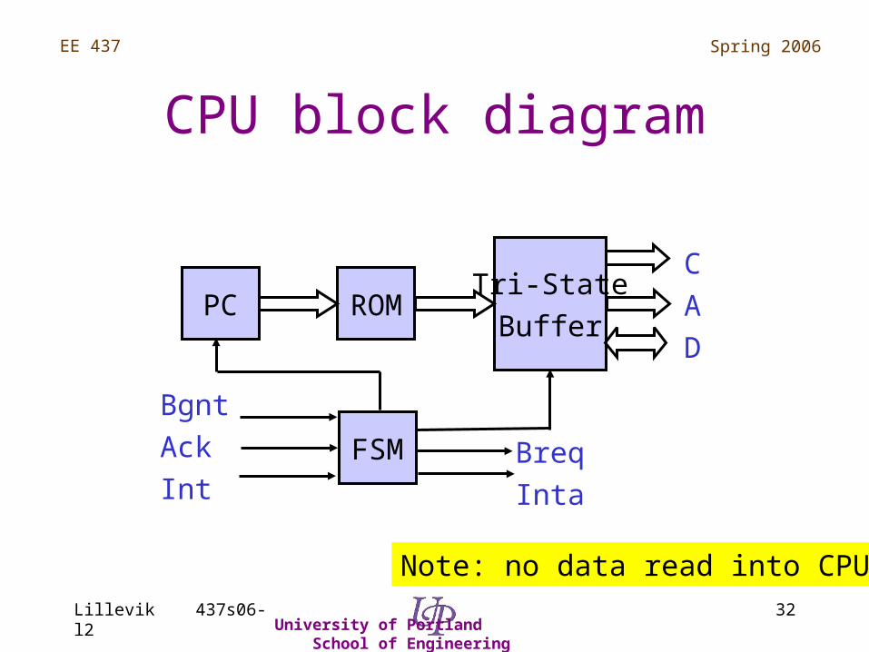
CPU block diagram
PC ROM
FSM
Tri-State
Buffer
Breq
Inta
Bgnt
Ack
Int
C
A
D
Note: no data read into CPU

Spring 2006
Lillevik 437s06-l2 33University of Portland School of Engineering
EE 437
CPU schematic
Next project

Spring 2006
Lillevik 437s06-l2 34University of Portland School of Engineering
EE 437

Spring 2006
Lillevik 437s06-l2 35University of Portland School of Engineering
EE 437
Find the Implementation ?
0 1
2 3
Q0
Q1
IN0
IN0
S
0
1
2
3
Din
Q1,Q0
LS153
IN1·IN0
1
IN0
IN1·IN0
IN0
1
2

Spring 2006
Lillevik 437s06-l2 36University of Portland School of Engineering
EE 437
ROM text file?Address Data
1 1
3 1
7 1
8 1
a 1
c 1
d 1
e 1
f 1

Spring 2006
Lillevik 437s06-l2 37University of Portland School of Engineering
EE 437
Example Buses?
• PCI: peripheral component interchange
• SCSI: small computer system interchange
• AGP: accelerated graphics port
• USB: universal serial bus
• HIPPI: high performance parallel interface
• IEEE 1394 (Fire Wire): faster USB
Spring 2006
Lillevik 437s06-l2 38University of Portland School of Engineering
EE 437
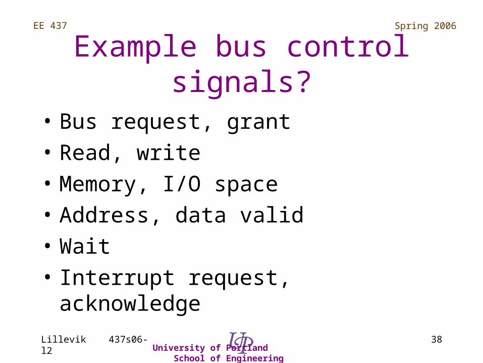
Example bus control signals?
• Bus request, grant
• Read, write
• Memory, I/O space
• Address, data valid
• Wait
• Interrupt request, acknowledge