springer handbook of electronic and photonic materials978-0-387-29185-7/1.pdf · in the...
TRANSCRIPT

Springer Handbookof Electronic and Photonic Materials

Springer Handbooks providea concise compilation of approvedkey information on methods ofresearch, general principles, andfunctional relationships in physi-cal sciences and engineering. Theworld’s leading experts in the fieldsof physics and engineering will beassigned by one or several renownededitors to write the chapters com-prising each volume. The contentis selected by these experts fromSpringer sources (books, journals,online content) and other systematicand approved recent publications ofphysical and technical information.
The volumes are designed to beuseful as readable desk referencebooks to give a fast and comprehen-sive overview and easy retrieval ofessential reliable key information,including tables, graphs, and bibli-ographies. References to extensivesources are provided.

123
HandbookSpringerof Electronic
and Photonic MaterialsSafa Kasap, Peter Capper (Eds.)
With CD-ROM, 930 Figures and 168 Tables

Editors:Safa KasapUniversity of SaskatchewanDepartment of Electrical EngineeringSaskatoon, SK, S7N 5A9Canada
Peter CapperSELEX Sensors and Airborne Systems Infrared Ltd.Millbrook Industrial EstateSouthampton, Hampshire SO15 0EGUnited Kingdom
Assistant Editor:Cyril KoughiaUniversity of SaskatchewanCanada
Library of Congress Control Number: 2006921596
ISBN-10: 0-387-26059-5 e-ISBN: 0-387-29185-7ISBN-13: 978-0-387-26059-4 Printed on acid free paper
c© 2006, Springer Science+Business Media, Inc.All rights reserved. This work may not be translated or copied in whole orin part without the written permission of the publisher (Springer Science+Business Media, Inc., 233 Spring Street, New York, NY 10013, USA), exceptfor brief excerpts in connection with reviews or scholarly analysis. Use inconnection with any form of information storage and retrieval, electronicadaptation, computer software, or by similar or dissimilar methodology nowknown or hereafter developed is forbidden. The use in this publication oftrade names, trademarks, service marks, and similar terms, even if they arenot identified as such, is not to be taken as an expression of opinion as towhether or not they are subject to proprietary rights.
The use of designations, trademarks, etc. in this publication does not imply,even in the absence of a specific statement, that such names are exempt fromthe relevant protective laws and regulations and therefore free for generaluse.
Product liability: The publisher cannot guarantee the accuracy of anyinformation about dosage and application contained in this book. In everyindividual case the user must check such information by consulting therelevant literature.
Production and typesetting: LE-TeX GbR, LeipzigHandbook coordinator: Dr. W. Skolaut, HeidelbergTypography, layout and illustrations:schreiberVIS, Seeheim & Hippmann GbR, SchwarzenbruckCover design: eStudio Calamar Steinen, BarcelonaCover production: WMXDesign GmbH, HeidelbergPrinting and binding: Stürtz GmbH, Würzburg
SPIN 11051855 9065/3141/YL 5 4 3 2 1 0

V
Foreword
The Editors, Authors, and Publisher are to be congrat-ulated on this distinguished volume, which will be aninvaluable source of information to all workers in thearea of electronic and photonic materials. Having madecontributions to earlier handbooks, I am well aware ofthe considerable, and sustained work that is necessary toproduce a volume of this kind. This particular handbook,however, is distinguished by its breadth of coverage inthe field, and the way in which it discusses the very lat-est developments. In such a rapidly moving field, this isa considerable challenge, and it has been met admirably.
Previous handbooks and encyclopaedia have tendedto concentrate on semiconducting materials, for theunderstandable reason of their dominance in the elec-tronics field, and the wide range of semiconductingmaterials and phenomena that must be covered. Fewhave been courageous enough to predict future trends,but in 1992 Mahajan and Kimerling attempted thisin the Introduction to their Concise Encyclopaediaof Semiconducting Materials and Related Technolo-gies (Pergamon), and foresaw future challenges inthe areas of nanoelectronics, low dislocation-densityIII-V substrates, semi-insulating III-V substrates, pat-terned epitaxy of III-Vs, alternative dielectrics andcontacts for silicon technology, and developments inion-implantation and diffusion. To a greater or lesserextent, all of these have been proved to be true, but itillustrates how difficult it is to make such a prediction.
Not many people would have thought, a decadeago, that the III-nitrides would occupy an importantposition in this book. As high melting point mater-ials, with the associated growth problems, they werenot high on the list of favourites for light emitters atthe blue end of the spectrum! The story is a fascinat-ing one – at least as interesting as the solution to theproblem of the short working life of early solid-statelasers at the red end of the spectrum. Optoelectron-ics and photonics, in general, have seen one of themost spectacular advances over the last decade, andthis is fully reflected in the book, ranging from visiblelight emitters, to infra-red materials. The book coversa wide range of work in Part D, including III-V and II-VI optoelectronic materials and band-gap engineering,as well as photonic glasses, liquid crystals, organic
Prof. Arthur WilloughbyMaterials Research Group,University of Southampton,UK
photoconductors, and the new areaof photonic crystals. The whole Partreflects materials for light genera-tion, processing, transmission anddetection – all the essential ele-ments for using light instead ofelectrons.
In the Materials for Electronicspart (Part C) the book charts theprogress in silicon – overwhelm-ingly the dominant material fora whole range of electronic func-tions and circuitry – including newdielectrics and other issues asso-ciated with shrinking geometry ofcircuits and devices to produce ever higher packingdensities. It also includes areas rarely covered in otherbooks – thick films, high-temperature electronic ma-terials, amorphous and microcrystalline materials. Theexisting developments that extend the life of silicon tech-nology, including silicon/germanium alloys, appear too,and raise the question again as to whether the predictedtimetable for the demise of silicon has again been de-clared too early!! Ferroelectrics – a class of materialsused so effectively in conjunction with silicon – certainlydeserve to be here.
The chapters in Part E (Novel Materials and Se-lected Applications), break new ground in a numberof admirable ways. Most of us are aware of, and fre-quently use, information recording devices such as CDs,videos, DVDs etc., but few are aware of the materials,or principles, involved. This book describes magneticinformation storage materials, as well as phase-changeoptical recording, keeping us fully up-to-date with recentdevelopments. The chapters also include applicationssuch as solar cells, sensors, photoconductors, and car-bon nanotubes, on which such a huge volume of workis presently being pursued worldwide. Both ends of thespectrum from research to applications are representedin chapters on molecular electronics and packagingmaterials.
A particular strength of this book is that it rangesfrom the fundamental science (Part A) through growthand characterisation of the materials (Part B) to

VI
applications (Parts C–E). Virtually all the materials cov-ered here have a wide range of applications, which isone of the reasons why this book is going to be souseful. As I indicated before, few of us will be suc-cessful in predicting the future direction and trends,
occupying the high-ground in this field in the comingdecade, but this book teaches us the basic principlesof materials, and leaves it to us to adapt these tothe needs of tomorrow. I commend it to you mostwarmly.
VII
Preface
Other handbooks in various disciplines such as electricalengineering, electronics, biomedical engineering, mater-ials science, etc. are currently available and well used bynumerous students, instructors and professionals. Mostlibraries have these handbook sets and each containsnumerous (at least 50) chapters that cover a wide spec-trum of topics within each well-defined discipline. Thesubject and the level of coverage appeal to both under-graduate and postgraduate students and researchers aswell as to practicing professionals. The advanced topicsfollow introductory topics and provide ample informa-tion that is useful to all, beginners and researchers, inthe field. Every few years, a new edition is brought outto update the coverage and include new topics.
There has been no similar handbook in electronicand photonic materials, and the present Springer Hand-book of Electronic and Photonic Materials (SHEPM)idea grew out of a need for a handbook that coversa wide spectrum of topics in materials that today’s engi-neers, material scientists, physicists, and chemists need.Electronic and photonic materials is a truly interdisci-plinary subject that encompasses a number of traditionaldisciplines such as materials science, electrical engi-neering, chemical engineering, mechanical engineering,physics and chemistry. It is not unusual to find a me-chanical engineering faculty carrying out research onelectronic packaging and electrical engineers carryingout characterization measurements on semiconductors.There are only a few established university departmentsin electronic or photonic materials. In general, electronicmaterials as a “discipline” appears as a research groupor as an interdisciplinary activity within a “college”.One could argue that, because of the very fact that it issuch an interdisciplinary field, there is a greater needto have a handbook that covers not only fundamen-tal topics but also advanced topics; hence the presenthandbook.
This handbook is a comprehensive treatise on elec-tronic and photonic materials with each chapter writtenby experts in the field. The handbook is aimed at seniorundergraduate and graduate students, researchers andprofessionals working in the area of electronic, opto-electronic and photonic materials. The chapters providethe necessary background and up-to-date knowledge
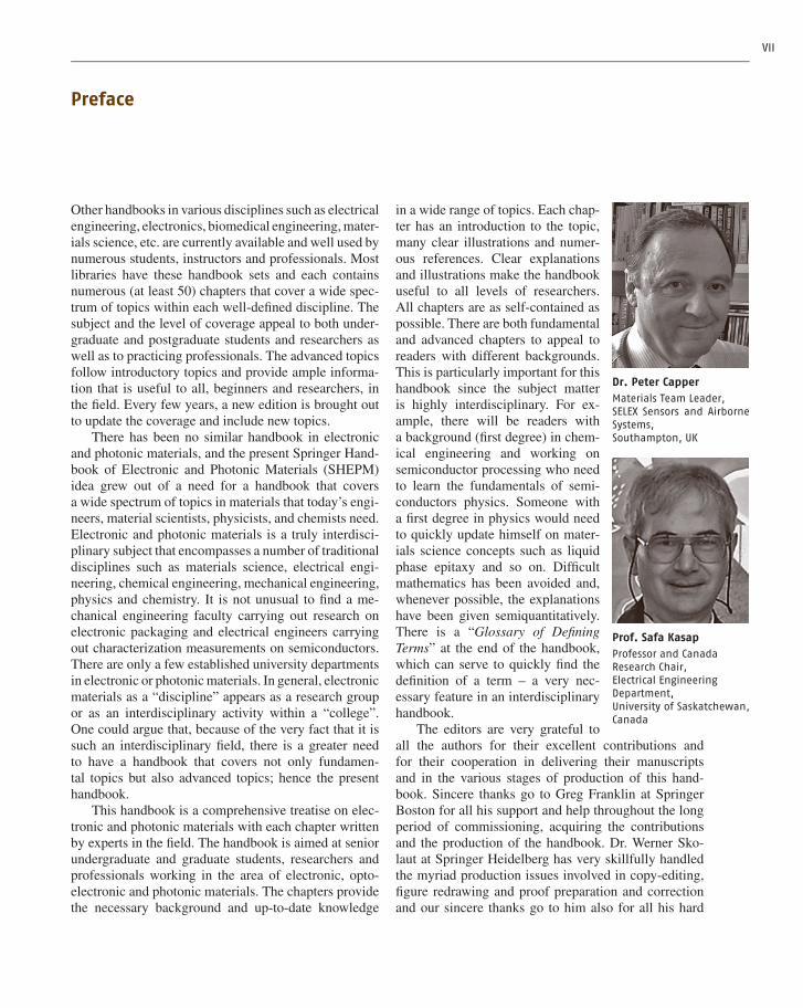
Dr. Peter CapperMaterials Team Leader,SELEX Sensors and AirborneSystems,Southampton, UK
Prof. Safa KasapProfessor and CanadaResearch Chair,Electrical EngineeringDepartment,University of Saskatchewan,Canada
in a wide range of topics. Each chap-ter has an introduction to the topic,many clear illustrations and numer-ous references. Clear explanationsand illustrations make the handbookuseful to all levels of researchers.All chapters are as self-contained aspossible. There are both fundamentaland advanced chapters to appeal toreaders with different backgrounds.This is particularly important for thishandbook since the subject matteris highly interdisciplinary. For ex-ample, there will be readers witha background (first degree) in chem-ical engineering and working onsemiconductor processing who needto learn the fundamentals of semi-conductors physics. Someone witha first degree in physics would needto quickly update himself on mater-ials science concepts such as liquidphase epitaxy and so on. Difficultmathematics has been avoided and,whenever possible, the explanationshave been given semiquantitatively.There is a “Glossary of DefiningTerms” at the end of the handbook,which can serve to quickly find thedefinition of a term – a very nec-essary feature in an interdisciplinaryhandbook.
The editors are very grateful toall the authors for their excellent contributions andfor their cooperation in delivering their manuscriptsand in the various stages of production of this hand-book. Sincere thanks go to Greg Franklin at SpringerBoston for all his support and help throughout the longperiod of commissioning, acquiring the contributionsand the production of the handbook. Dr. Werner Sko-laut at Springer Heidelberg has very skillfully handledthe myriad production issues involved in copy-editing,figure redrawing and proof preparation and correctionand our sincere thanks go to him also for all his hard

VIII
work in making the handbook attractive to read. He is themost dedicated and efficient editor we have come across.
It is a pleasure to thank Professor Arthur Willoughbyfor his many helpful suggestions that made this a betterhandbook. His wealth of experience as editor of theJournal of Materials Science: Materials in Electronicsplayed an important role not only in selecting chaptersbut also in finding the right authors.
Finally, the editors wish to thank all the members ofour families (Marian, Samuel and Thomas; and Nicol-lette) for their support and particularly their enduranceduring the entire project.
Peter Capper and Safa KasapEditors
IX
List of Authors
Martin Abkowitz1198 Gatestone CircleWebster, NY 14580, USAe-mail: [email protected],[email protected]
Sadao AdachiGunma UniversityDepartment of Electronic Engineering,Faculty of EngineeringKiryu-shi 376-8515Gunma, Japane-mail: [email protected]
Alfred AdamsUniversity of SurreyAdvanced Technology InstituteGuildford, Surrey, GU2 7XH,Surrey, UKe-mail: [email protected]
Guy J. AdriaenssensUniversity of LeuvenLaboratorium voor HalfgeleiderfysicaCelestijnenlaan 200DB-3001 Leuven, Belgiume-mail: [email protected]
Wilfried von AmmonSiltronic AGResearch and DevelopmentJohannes Hess Strasse 2484489 Burghausen, Germanye-mail: [email protected]
Peter AshburnUniversity of SouthamptonSchool of Electronics and Computer ScienceSouthampton, SO17 1BJ, UKe-mail: [email protected]
Mark AuslenderBen-Gurion University of the Negev Beer ShevaDepartment of Electricaland Computer EngineeringP.O.Box 653Beer Sheva 84105, Israele-mail: [email protected]
Darren M. BagnallUniversity of SouthamptonSchool of Electronics and Computer ScienceSouthampton, SO17 1BJ, UKe-mail: [email protected]
Ian M. BakerSELEX Sensors and Airborne Systems Infrared Ltd.Southampton, Hampshire SO15 OEG, UKe-mail: [email protected]
Sergei BaranovskiiPhilipps University MarburgDepartment of PhysicsRenthof 535032 Marburg, Germanye-mail: [email protected]
Mark BaxendaleQueen Mary, University of LondonDepartment of PhysicsMile End RoadLondon, E1 4NS, UKe-mail: [email protected]
Mohammed L. BenkhedirUniversity of LeuvenLaboratorium voor HalfgeleiderfysicaCelestijnenlaan 200DB-3001 Leuven, Belgiume-mail: [email protected]
X List of Authors
Monica BrinzaUniversity of LeuvenLaboratorium voor HalfgeleiderfysicaCelestijnenlaan 200DB-3001 Leuven, Belgiume-mail: [email protected]
Paul D. BrownUniversity of NottinghamSchool of Mechanical, Materials andManufacturing EngineeringUniversity ParkNottingham, NG7 2RD, UKe-mail: [email protected]
Mike BrozelUniversity of GlasgowDepartment of Physics and AstronomyKelvin BuildingGlasgow, G12 8QQ, UKe-mail: [email protected]
Lukasz BrzozowskiUniversity of TorontoSunnybrook and Women’s Research Institute,Imaging Research/Department of Medical BiophysicsResearch Building, 2075 Bayview AvenueToronto, ON, M4N 3M5, Canadae-mail: [email protected]
Peter CapperSELEX Sensors and Airborne Systems Infrared Ltd.Materials Team LeaderMillbrook Industrial Estate, PO Box 217Southampton, Hampshire SO15 0EG, UKe-mail: [email protected]
Larry ComstockSan Jose State University6574 Crystal Springs DriveSan Jose, CA 95120, USAe-mail: [email protected]
Ray DeCorbyUniversity of AlbertaDepartment of Electricaland Computer Engineering7th Floor, 9107-116 Street N.W.Edmonton, Alberta T6G 2V4, Canadae-mail: [email protected]
M. Jamal DeenMcMaster UniversityDepartment of Electricaland Computer Engineering (CRL 226)1280 Main Street WestHamilton, ON L8S 4K1, Canadae-mail: [email protected]
Leonard DissadoThe University of LeicesterDepartment of EngineeringUniversity RoadLeicester, LE1 7RH, UKe-mail: [email protected]
David DunmurUniversity of SouthamptonSchool of ChemistrySouthampton, SO17 1BJ, UKe-mail: [email protected]
Lester F. EastmanCornell UniversityDepartment of Electricaland Computer Engineering425 Phillips HallIthaca, NY 14853, USAe-mail: [email protected]
Andy EdgarVictoria UniversitySchool of Chemical and Physical Sciences SCPSKelburn Parade/PO Box 600Wellington, New Zealande-mail: [email protected]

List of Authors XI
Brian E. FoutzCadence Design Systems1701 North Street, Bldg 257-3Endicott, NY 13760, USAe-mail: [email protected]
Mark FoxUniversity of SheffieldDepartment of Physics and AstronomyHicks Building, Hounsefield RoadSheffield, S3 7RH, UKe-mail: [email protected]
Darrel FrearRF and Power Packaging Technology Development,Freescale Semiconductor2100 East Elliot RoadTempe, AZ 85284, USAe-mail: [email protected]
Milan FrieselChalmers University of TechnologyDepartment of PhysicsFysikgränd 341296 Göteborg, Swedene-mail: [email protected]
Jacek GieraltowskiUniversité de Bretagne Occidentale6 Avenue Le Gorgeu, BP: 80929285 Brest Cedex, Francee-mail: [email protected]
Yinyan GongColumbia UniversityDepartment of Applied Physicsand Applied Mathematics500 W. 120th St.New York, NY 10027, USAe-mail: [email protected]
Robert D. Gould†
Keele UniversityThin Films Laboratory, Department of Physics,School of Chemistry and PhysicsKeele, Staffordshire ST5 5BG, UK
Shlomo HavaBen-Gurion University of the Negev Beer ShevaDepartment of Electricaland Computer EngineeringP.O. Box 653Beer Sheva 84105, Israele-mail: [email protected]
Colin HumphreysUniversity of CambridgeDepartment of Materials Science and MetallurgyPembroke StreetCambridge, CB2 3!Z, UKe-mail: [email protected]
Stuart IrvineUniversity of Wales, BangorDepartment of ChemistryGwynedd, LL57 2UW, UKe-mail: [email protected]
Minoru IsshikiTohoku UniversityInstitute of Multidisciplinary Researchfor Advanced Materials1-1, Katahira, 2 chome, AobakuSendai, 980-8577, Japane-mail: [email protected]
Robert JohansonUniversity of SaskatchewanDepartment of Electrical Engineering57 Campus DriveSaskatoon, SK S7N 5A9, Canadae-mail: [email protected]
Tim JoyceUniversity of LiverpoolFunctional Materials Research Centre,Department of EngineeringBrownlow HillLiverpool, L69 3BX, UKe-mail: [email protected]
XII List of Authors
M. Zahangir KabirConcordia UniversityDepartment of Electrical and ComputerEngineeringMontreal, Quebec S7N5A9, Canadae-mail: [email protected]
Safa KasapUniversity of SaskatchewanDepartment of Electrical Engineering57 Campus DriveSaskatoon, SK S7N 5A9, Canadae-mail: [email protected]
Alexander KolobovNational Institute of AdvancedIndustrial Science and TechnologyCenter for Applied Near-Field Optics Research1-1-1 Higashi, TsukubaIbaraki, 305-8562, Japane-mail: [email protected]
Cyril KoughiaUniversity of SaskatchewanDepartment of Electrical Engineering57 Campus DriveSaskatoon, SK S7N 5A9, Canadae-mail: [email protected]
Igor L. KuskovskyQueens College, City University of New York (CUNY)Department of Physics65-30 Kissena Blvd.Flushing, NY 11367, USAe-mail: [email protected]
Geoffrey LuckhurstUniversity of SouthamptonSchool of ChemistrySouthampton, SO17 1BJ, UKe-mail: [email protected]
Akihisa MatsudaTokyo University of ScienceResearch Institute for Science and Technology2641 Yamazaki, Noda-shiChiba, 278-8510, Japane-mail: [email protected],[email protected]
Naomi MatsuuraSunnybrook Health Sciences CentreDepartment of Medical Biophysics,Imaging Research2075 Bayview AvenueToronto, ON M4N 3M5, Canadae-mail: [email protected]
Kazuo MorigakiUniversity of TokyoC-305, Wakabadai 2-12, InagiTokyo, 206-0824, Japane-mail: [email protected]
Hadis MorkoçVirginia Commonwealth UniversityDepartment of Electricaland Computer Engineering601 W. Main St., Box 843072Richmond, VA 23284-3068, USAe-mail: [email protected]
Winfried MönchUniversität Duisburg-EssenLotharstraße 147048 Duisburg, Germanye-mail: [email protected]
Arokia NathanUniversity of WaterlooDepartment of Electricaland Computer Engineering200 University Avenue W.Waterloo, Ontario N2L 3G1, Canadae-mail: [email protected]

List of Authors XIII
Gertrude F. NeumarkColumbia UniversityDepartment of Applied Physicsand Applied Mathematics500W 120th St., MC 4701New York, NY 10027, USAe-mail: [email protected]
Stephen K. O’LearyUniversity of ReginaFaculty of Engineering3737 Wascana ParkwayRegina, SK S4S 0A2, Canadae-mail: [email protected]
Chisato OgiharaYamaguchi UniversityDepartment of Applied Science2-16-1 TokiwadaiUbe, 755-8611, Japane-mail: [email protected]
Fabien PascalUniversité Montpellier 2/CEM2-cc084Centre d’Electroniqueet de Microoptoélectronique de MontpellierPlace E. Bataillon34095 Montpellier, Francee-mail: [email protected]
Michael PettyUniversity of DurhamDepartment School of EngineeringSouth RoadDurham, DH1 3LE, UKe-mail: [email protected]
Asim Kumar RayQueen Mary, University of LondonDepartment of MaterialsMile End RoadLondon, E1 4NS, UKe-mail: [email protected]
John RowlandsUniversity of TorontoDepartment of Medical BiophysicsSunnybrook and Women’s CollegeHealth Sciences CentreS656-2075 Bayview AvenueToronto, ON M4N 3M5, Canadae-mail: [email protected]
Oleg RubelPhilipps University MarburgDepartment of Physicsand Material Sciences CenterRenthof 535032 Marburg, Germanye-mail: [email protected]
Harry RudaUniversity of TorontoMaterials Science and Engineering,Electrical and Computer Engineering170 College StreetToronto, M5S 3E4, Canadae-mail: [email protected]
Edward SargentUniversity of TorontoDepartment of Electricaland Computer EngineeringECE, 10 King’s College RoadToronto, M5S 3G4, Canadae-mail: [email protected]
Peyman ServatiIgnis Innovation Inc.55 Culpepper Dr.Waterloo, Ontario N2L 5K8, Canadae-mail: [email protected]
Derek ShawHull UniversityHull, HU6 7RX, UKe-mail: [email protected]

XIV List of Authors
Fumio ShimuraShizuoka Institute of Science and TechnologyDepartment of Materials and Life Science2200-2 ToyosawaFukuroi, Shizuoka 437-8555, Japane-mail: [email protected]
Michael ShurRenssellaer Polytechnic InstituteDepartment of Electrical, Computer,and Systems EngineeringCII 9017, RPI, 110 8th StreetTroy, NY 12180, USAe-mail: [email protected]
Jai SinghCharles Darwin UniversitySchool of Engineering and Logistics,Faculty of Technology, B-41Ellengowan DriveDarwin, NT 0909, Australiae-mail: [email protected]
Tim SmeetonSharp Laboratories of EuropeEdmund Halley Road, Oxford Science ParkOxford, OX4 4GB, UKe-mail: [email protected]
Boris StraumalRussian Academy of SciencesInstitute of Sold State PhysicsInstitutskii prospect 15Chernogolovka, 142432, Russiae-mail: [email protected]
Stephen SweeneyUniversity of SurreyAdvanced Technology InstituteGuildford, Surrey GU2 7XH, UKe-mail: [email protected]
David SykesLoughborough Surface Analysis Ltd.PO Box 5016, Unit FC, Holywell Park, Ashby RoadLoughborough, LE11 3WS, UKe-mail: [email protected]
Keiji TanakaHokkaido UniversityDepartment of Applied Physics,Graduate School of EngineeringKita-ku, N13 W8Sapporo, 060-8628, Japane-mail: [email protected]
Charbel TannousUniversité de Bretagne OccidentaleLMB, CNRS FRE 26976 Avenue Le Gorgeu, BP: 80929285 Brest Cedex, Francee-mail: [email protected]
Ali TekeBalikesir UniversityDepartment of Physics, Faculty of Art and ScienceBalikesir, 10100, Turkeye-mail: [email protected]
Junji TominagaNational Institute of Advanced IndustrialScience and Technology, AISTCenter for Applied Near-Field Optics Research,CAN-FORTsukuba Central 4 1-1-1 HigashiTsukuba, 3.5-8562, Japane-mail: [email protected]
Dan TonchevUniversity of SaskatchewanDepartment of Electrical Engineering57 Campus DriveSaskatoon, SK S7N 5A9, Canadae-mail: [email protected]
Harry L. TullerMassachusetts Institute of TechnologyDepartment of Materials Science and Engineering,Crystal Physics and Electroceramics Laboratory77 Massachusetts AvenueCambridge, MA 02139, USAe-mail: [email protected]
List of Authors XV
Qamar-ul WahabLinköping UniversityDepartment of Physics,Chemistry, and Biology (IFM)SE-581 83 Linköping, Swedene-mail: [email protected]
Robert M. WallaceUniversity of Texas at DallasDepartment of Electrical EngineeringM.S. EC 33, P.O.Box 830688Richardson, TX 75083, USAe-mail: [email protected]
Jifeng WangTohoku UniversityInstitute of Multidisciplinary Researchfor Advanced Materials1-1, Katahira, 2 Chome, AobakuSendai, 980-8577, Japane-mail: [email protected]
David S. WeissNexPress Solutions, Inc.2600 Manitou RoadRochester, NY 14653-4180, USAe-mail: [email protected]
Rainer WescheSwiss Federal Institute of TechnologyCentre de Recherches en Physique des PlasmasCRPP (c/o Paul Scherrer Institute), WMHA/C31,Villigen PSLausanne, CH-5232, Switzerlande-mail: [email protected]
Roger WhatmoreTyndall National InstituteLee Maltings, Cork , Irelande-mail: [email protected]
Neil WhiteUniversity of SouthamptonSchool of Electronics and Computer ScienceMountbatten BuildingHighfield, Southampton SO17 1BJ, UKe-mail: [email protected]
Magnus WillanderUniversity of GothenburgDepartment of PhysicsSE-412 96 Göteborg, Swedene-mail: [email protected]
Jan WillekensUniversity of LeuvenLaboratorium voor HalfgeleiderfysicaCelestijnenlaan 200DB-3001 Leuven, Belgiume-mail: [email protected]
XVII
Contents
List of Abbreviations ................................................................................. XXIX
Introduction
1 Perspectives on Electronic and Optoelectronic Materials.................. 31.1 The Early Years .............................................................................. 41.2 The Silicon Age .............................................................................. 41.3 The Compound Semiconductors ...................................................... 81.4 From Faraday to Today .................................................................. 14References............................................................................................... 14
Part A Fundamental Properties
2 Electrical Conduction in Metals and Semiconductors ........................ 192.1 Fundamentals: Drift Velocity, Mobility and Conductivity .................. 202.2 Matthiessen’s Rule ........................................................................ 222.3 Resistivity of Metals ....................................................................... 232.4 Solid Solutions and Nordheim’s Rule .............................................. 262.5 Carrier Scattering in Semiconductors .............................................. 282.6 The Boltzmann Transport Equation ................................................. 292.7 Resistivity of Thin Polycrystalline Films ........................................... 302.8 Inhomogeneous Media. Effective Media Approximation .................. 322.9 The Hall Effect ............................................................................... 352.10 High Electric Field Transport ........................................................... 372.11 Avalanche ..................................................................................... 382.12 Two-Dimensional Electron Gas ....................................................... 392.13 One Dimensional Conductance ....................................................... 412.14 The Quantum Hall Effect ................................................................ 42References............................................................................................... 44
3 Optical Properties of Electronic Materials:Fundamentals and Characterization .................................................. 473.1 Optical Constants ........................................................................... 473.2 Refractive Index ............................................................................ 503.3 Optical Absorption ......................................................................... 533.4 Thin Film Optics............................................................................. 703.5 Optical Materials ........................................................................... 74References............................................................................................... 76
XVIII Contents
4 Magnetic Properties of Electronic Materials ...................................... 794.1 Traditional Magnetism ................................................................... 814.2 Unconventional Magnetism ........................................................... 93References............................................................................................... 99
5 Defects in Monocrystalline Silicon ...................................................... 1015.1 Technological Impact of Intrinsic Point Defects Aggregates .............. 1025.2 Thermophysical Properties of Intrinsic Point Defects ........................ 1035.3 Aggregates of Intrinsic Point Defects ............................................... 1045.4 Formation of OSF Ring ................................................................... 115References............................................................................................... 117
6 Diffusion in Semiconductors ............................................................... 1216.1 Basic Concepts .............................................................................. 1226.2 Diffusion Mechanisms ................................................................... 1226.3 Diffusion Regimes ......................................................................... 1236.4 Internal Electric Fields ................................................................... 1266.5 Measurement of Diffusion Coefficients............................................ 1266.6 Hydrogen in Semiconductors ......................................................... 1276.7 Diffusion in Group IV Semiconductors ............................................. 1286.8 Diffusion in III–V Compounds ......................................................... 1306.9 Diffusion in II–VI Compounds ......................................................... 1316.10 Conclusions ................................................................................... 1336.11 General Reading and References .................................................... 133References............................................................................................... 133
7 Photoconductivity in Materials Research ........................................... 1377.1 Steady State Photoconductivity Methods ........................................ 1387.2 Transient Photoconductivity Experiments ....................................... 142References............................................................................................... 146
8 Electronic Properties of Semiconductor Interfaces ............................ 1478.1 Experimental Database .................................................................. 1498.2 IFIGS-and-Electronegativity Theory ................................................ 1538.3 Comparison of Experiment and Theory ........................................... 1558.4 Final Remarks ............................................................................... 159References............................................................................................... 159
9 Charge Transport in Disordered Materials.......................................... 1619.1 General Remarks on Charge Transport in Disordered Materials ......... 1639.2 Charge Transport in Disordered Materials via Extended States .......... 1679.3 Hopping Charge Transport in Disordered Materials
via Localized States ....................................................................... 1699.4 Concluding Remarks ...................................................................... 184References............................................................................................... 185

Contents XIX
10 Dielectric Response .............................................................................. 18710.1 Definition of Dielectric Response .................................................... 18810.2 Frequency-Dependent Linear Responses ........................................ 19010.3 Information Contained in the Relaxation Response ......................... 19610.4 Charge Transport ........................................................................... 20810.5 A Few Final Comments ................................................................... 211References............................................................................................... 211
11 Ionic Conduction and Applications ..................................................... 21311.1 Conduction in Ionic Solids.............................................................. 21411.2 Fast Ion Conduction ....................................................................... 21611.3 Mixed Ionic–Electronic Conduction................................................. 22111.4 Applications .................................................................................. 22311.5 Future Trends ................................................................................ 226References............................................................................................... 226
Part B Growth and Characterization
12 Bulk Crystal Growth – Methods and Materials .................................. 23112.1 History .......................................................................................... 23212.2 Techniques ................................................................................... 23312.3 Materials Grown ............................................................................ 24012.4 Conclusions ................................................................................... 251References............................................................................................... 251
13 Single-Crystal Silicon: Growth and Properties................................... 25513.1 Overview....................................................................................... 25613.2 Starting Materials .......................................................................... 25713.3 Single-Crystal Growth .................................................................... 25813.4 New Crystal Growth Methods ......................................................... 266References............................................................................................... 268
14 Epitaxial Crystal Growth: Methods and Materials ............................. 27114.1 Liquid-Phase Epitaxy (LPE) ............................................................. 27114.2 Metalorganic Chemical Vapor Deposition (MOCVD)............................ 28014.3 Molecular Beam Epitaxy (MBE) ....................................................... 290References............................................................................................... 299
15 Narrow-Bandgap II–VI Semiconductors: Growth .............................. 30315.1 Bulk Growth Techniques ................................................................ 30415.2 Liquid-Phase Epitaxy (LPE) ............................................................. 30815.3 Metalorganic Vapor Phase Epitaxy (MOVPE) ..................................... 31215.4 Molecular Beam Epitaxy (MBE) ....................................................... 31715.5 Alternatives to CMT ........................................................................ 320References............................................................................................... 321

XX Contents
16 Wide-Bandgap II–VI Semiconductors:Growth and Properties ........................................................................ 32516.1 Crystal Properties .......................................................................... 32616.2 Epitaxial Growth ........................................................................... 32816.3 Bulk Crystal Growth ....................................................................... 33316.4 Conclusions ................................................................................... 339References............................................................................................... 340
17 Structural Characterization.................................................................. 34317.1 Radiation–Material Interactions..................................................... 34417.2 Particle–Material Interactions ........................................................ 34517.3 X-Ray Diffraction ........................................................................... 34817.4 Optics, Imaging and Electron Diffraction ......................................... 35117.5 Characterizing Functional Activity ................................................... 36217.6 Sample Preparation ....................................................................... 36217.7 Case Studies – Complementary Characterization of Electronic
and Optoelectronic Materials ......................................................... 36417.8 Concluding Remarks ...................................................................... 370References............................................................................................... 370
18 Surface Chemical Analysis .................................................................... 37318.1 Electron Spectroscopy .................................................................... 37318.2 Glow-Discharge Spectroscopies (GDOES and GDMS) .......................... 37618.3 Secondary Ion Mass Spectrometry (SIMS) ......................................... 37718.4 Conclusion .................................................................................... 384
19 Thermal Properties and Thermal Analysis:Fundamentals, Experimental Techniquesand Applications .................................................................................. 38519.1 Heat Capacity ................................................................................ 38619.2 Thermal Conductivity ..................................................................... 39119.3 Thermal Expansion ........................................................................ 39619.4 Enthalpic Thermal Properties ......................................................... 39819.5 Temperature-Modulated DSC (TMDSC) ............................................. 403References............................................................................................... 406
20 Electrical Characterization of Semiconductor Materialsand Devices........................................................................................... 40920.1 Resistivity ..................................................................................... 41020.2 Hall Effect ..................................................................................... 41820.3 Capacitance–Voltage Measurements ............................................... 42120.4 Current–Voltage Measurements ..................................................... 42620.5 Charge Pumping ............................................................................ 42820.6 Low-Frequency Noise .................................................................... 43020.7 Deep-Level Transient Spectroscopy ................................................. 434References............................................................................................... 436

Contents XXI
Part C Materials for Electronics
21 Single-Crystal Silicon: Electrical and Optical Properties ................... 44121.1 Silicon Basics ................................................................................ 44121.2 Electrical Properties ....................................................................... 45121.3 Optical Properties .......................................................................... 472References............................................................................................... 478
22 Silicon–Germanium: Properties, Growth and Applications .............. 48122.1 Physical Properties of Silicon–Germanium ...................................... 48222.2 Optical Properties of SiGe ............................................................... 48822.3 Growth of Silicon–Germanium ....................................................... 49222.4 Polycrystalline Silicon–Germanium ................................................ 494References............................................................................................... 497
23 Gallium Arsenide .................................................................................. 49923.1 Bulk Growth of GaAs ...................................................................... 50223.2 Epitaxial Growth of GaAs ............................................................... 50723.3 Diffusion in Gallium Arsenide ........................................................ 51123.4 Ion Implantation into GaAs ............................................................ 51323.5 Crystalline Defects in GaAs ............................................................. 51423.6 Impurity and Defect Analysis of GaAs (Chemical) ............................. 51723.7 Impurity and Defect Analysis of GaAs (Electrical) ............................. 51823.8 Impurity and Defect Analysis of GaAs (Optical) ................................ 52123.9 Assessment of Complex Heterostructures ........................................ 52223.10 Electrical Contacts to GaAs ............................................................. 52423.11 Devices Based on GaAs (Microwave)................................................ 52423.12 Devices based on GaAs (Electro-optical) ......................................... 52723.13 Other Uses for GaAs ....................................................................... 53223.14 Conclusions ................................................................................... 532References............................................................................................... 533
24 High-Temperature Electronic Materials:Silicon Carbide and Diamond .............................................................. 53724.1 Material Properties and Preparation ............................................... 54024.2 Electronic Devices .......................................................................... 54724.3 Summary ...................................................................................... 557References............................................................................................... 558
25 Amorphous Semiconductors: Structure, Optical,and Electrical Properties...................................................................... 56525.1 Electronic States ............................................................................ 56525.2 Structural Properties ...................................................................... 56825.3 Optical Properties .......................................................................... 57025.4 Electrical Properties ....................................................................... 57325.5 Light-Induced Phenomena ............................................................ 57525.6 Nanosized Amorphous Structure..................................................... 577References............................................................................................... 578
XXII Contents
26 Amorphous and Microcrystalline Silicon ............................................ 58126.1 Reactions in SiH4 and SiH4/H2 Plasmas ........................................... 58126.2 Film Growth on a Surface .............................................................. 58326.3 Defect Density Determination for a-Si:H and µc-Si:H ...................... 58926.4 Device Applications ....................................................................... 59026.5 Recent Progress in Material Issues Related to Thin-Film
Silicon Solar Cells ........................................................................... 59126.6 Summary ...................................................................................... 594References............................................................................................... 594
27 Ferroelectric Materials ......................................................................... 59727.1 Ferroelectric Materials ................................................................... 60127.2 Ferroelectric Materials Fabrication Technology ................................ 60827.3 Ferroelectric Applications ............................................................... 616References............................................................................................... 622
28 Dielectric Materials for Microelectronics ............................................ 62528.1 Gate Dielectrics ............................................................................. 63028.2 Isolation Dielectrics ....................................................................... 64728.3 Capacitor Dielectrics ...................................................................... 64728.4 Interconnect Dielectrics ................................................................. 65128.5 Summary ...................................................................................... 653References............................................................................................... 653
29 Thin Films ............................................................................................. 65929.1 Deposition Methods ...................................................................... 66129.2 Structure ....................................................................................... 68229.3 Properties ..................................................................................... 69229.4 Concluding Remarks ...................................................................... 708References............................................................................................... 711
30 Thick Films ............................................................................................ 71730.1 Thick Film Processing ..................................................................... 71830.2 Substrates ..................................................................................... 72030.3 Thick Film Materials ....................................................................... 72130.4 Components and Assembly ............................................................ 72430.5 Sensors ......................................................................................... 728References............................................................................................... 731
Part D Materials for Optoelectronics and Photonics
31 III-V Ternary and Quaternary Compounds .......................................... 73531.1 Introduction to III–V Ternary and Quaternary Compounds ............... 73531.2 Interpolation Scheme .................................................................... 73631.3 Structural Parameters .................................................................... 73731.4 Mechanical, Elastic and Lattice Vibronic Properties.......................... 739

Contents XXIII
31.5 Thermal Properties ........................................................................ 74131.6 Energy Band Parameters ................................................................ 74331.7 Optical Properties .......................................................................... 74831.8 Carrier Transport Properties............................................................ 750References............................................................................................... 751
32 Group III Nitrides.................................................................................. 75332.1 Crystal Structures of Nitrides .......................................................... 75532.2 Lattice Parameters of Nitrides ........................................................ 75632.3 Mechanical Properties of Nitrides ................................................... 75732.4 Thermal Properties of Nitrides ........................................................ 76132.5 Electrical Properties of Nitrides ...................................................... 76632.6 Optical Properties of Nitrides.......................................................... 77732.7 Properties of Nitride Alloys............................................................. 79132.8 Summary and Conclusions ............................................................. 794References............................................................................................... 795
33 Electron Transport Within the III–V Nitride Semiconductors,GaN, AlN, and InN: A Monte Carlo Analysis ........................................ 80533.1 Electron Transport Within Semiconductors and the Monte Carlo
Simulation Approach ..................................................................... 80633.2 Steady-State and Transient Electron Transport
Within Bulk Wurtzite GaN, AlN, and InN .......................................... 81033.3 Electron Transport Within III–V Nitride Semiconductors: A Review .... 82233.4 Conclusions ................................................................................... 826References............................................................................................... 826
34 II–IV Semiconductors for Optoelectronics: CdS, CdSe, CdTe............... 82934.1 Background .................................................................................. 82934.2 Solar Cells ..................................................................................... 82934.3 Radiation Detectors ....................................................................... 83434.4 Conclusions ................................................................................... 840References............................................................................................... 840
35 Doping Aspects of Zn-Based Wide-Band-Gap Semiconductors ....... 84335.1 ZnSe ............................................................................................. 84335.2 ZnBeSe.......................................................................................... 84835.3 ZnO ............................................................................................... 849References............................................................................................... 851
36 II–VI Narrow-Bandgap Semiconductors for Optoelectronics ............ 85536.1 Applications and Sensor Design...................................................... 85836.2 Photoconductive Detectors in HgCdTe and Related Alloys ................. 86036.3 SPRITE Detectors ............................................................................ 86436.4 Photoconductive Detectors in Closely Related Alloys ........................ 86636.5 Conclusions on Photoconductive HgCdTe Detectors .......................... 86736.6 Photovoltaic Devices in HgCdTe ...................................................... 867

XXIV Contents
36.7 Emission Devices in II–VI Semiconductors ....................................... 88236.8 Potential for Reduced-Dimensionality HgTe–CdTe ........................... 883References............................................................................................... 883
37 Optoelectronic Devices and Materials ................................................. 88737.1 Introduction to Optoelectronic Devices ........................................... 88837.2 Light-Emitting Diodes and Semiconductor Lasers ............................ 89037.3 Single-Mode Lasers ....................................................................... 90437.4 Optical Amplifiers .......................................................................... 90637.5 Modulators ................................................................................... 90737.6 Photodetectors .............................................................................. 91137.7 Conclusions ................................................................................... 914References............................................................................................... 915
38 Liquid Crystals ...................................................................................... 91738.1 Introduction to Liquid Crystals ....................................................... 91738.2 The Basic Physics of Liquid Crystals ................................................. 92438.3 Liquid-Crystal Devices ................................................................... 93138.4 Materials for Displays .................................................................... 940References............................................................................................... 949
39 Organic Photoconductors..................................................................... 95339.1 Chester Carlson and Xerography ..................................................... 95439.2 Operational Considerations and Critical Materials Properties ............ 95639.3 OPC Characterization ...................................................................... 96539.4 OPC Architecture and Composition .................................................. 96739.5 Photoreceptor Fabrication ............................................................. 97639.6 Summary ...................................................................................... 977References............................................................................................... 978
40 Luminescent Materials ......................................................................... 98340.1 Luminescent Centres...................................................................... 98540.2 Interaction with the Lattice ........................................................... 98740.3 Thermally Stimulated Luminescence ............................................... 98940.4 Optically (Photo-)Stimulated Luminescence .................................... 99040.5 Experimental Techniques – Photoluminescence .............................. 99140.6 Applications .................................................................................. 99240.7 Representative Phosphors ............................................................. 995References............................................................................................... 995
41 Nano-Engineered Tunable Photonic Crystals in the Near-IRand Visible Electromagnetic Spectrum ............................................... 99741.1 PC Overview .................................................................................. 99841.2 Traditional Fabrication Methodologies for Static PCs ........................ 100141.3 Tunable PCs ................................................................................... 101141.4 Summary and Conclusions ............................................................. 1014References............................................................................................... 1015

Contents XXV
42 Quantum Wells, Superlattices, and Band-Gap Engineering............. 102142.1 Principles of Band-Gap Engineering and Quantum
Confinement ................................................................................. 102242.2 Optoelectronic Properties of Quantum-Confined Structures ............. 102442.3 Emitters ........................................................................................ 103242.4 Detectors ...................................................................................... 103442.5 Modulators ................................................................................... 103642.6 Future Directions ........................................................................... 103742.7 Conclusions ................................................................................... 1038References............................................................................................... 1038
43 Glasses for Photonic Integration ........................................................ 104143.1 Main Attributes of Glasses as Photonic Materials ............................. 104243.2 Glasses for Integrated Optics .......................................................... 105043.3 Laser Glasses for Integrated Light Sources ....................................... 105343.4 Summary ...................................................................................... 1057References............................................................................................... 1059
44 Optical Nonlinearity in Photonic Glasses ........................................... 106344.1 Third-Order Nonlinearity in Homogeneous Glass ............................. 106444.2 Second-Order Nonlinearity in Poled Glass....................................... 106944.3 Particle-Embedded Systems ........................................................... 107044.4 Photoinduced Phenomena ............................................................ 107144.5 Summary ...................................................................................... 1072References............................................................................................... 1072
45 Nonlinear Optoelectronic Materials .................................................... 107545.1 Background .................................................................................. 107545.2 Illumination-Dependent Refractive Index and Nonlinear
Figures of Merit (FOM) .................................................................... 107745.3 Bulk and Multi-Quantum-Well (MQW) Inorganic
Crystalline Semiconductors ............................................................ 108045.4 Organic Materials .......................................................................... 108445.5 Nanocrystals ................................................................................. 108745.6 Other Nonlinear Materials .............................................................. 108845.7 Conclusions ................................................................................... 1089References............................................................................................... 1089
Part E Novel Materials and Selected Applications
46 Solar Cells and Photovoltaics .............................................................. 109546.1 Figures of Merit for Solar Cells ........................................................ 109646.2 Crystalline Silicon .......................................................................... 109846.3 Amorphous Silicon ........................................................................ 110046.4 GaAs Solar Cells ............................................................................. 110146.5 CdTe Thin-Film Solar Cells .............................................................. 1102
XXVI Contents
46.6 CuInGaSe2 (CIGS) Thin-Film Solar Cells ............................................. 110346.7 Conclusions ................................................................................... 1104References............................................................................................... 1105
47 Silicon on Mechanically Flexible Substrates for Large-AreaElectronics............................................................................................. 110747.1 a-Si:H TFTs on Flexible Substrates .................................................. 110847.2 Field-Effect Transport in Amorphous Films ..................................... 110847.3 Electronic Transport Under Mechanical Stress .................................. 1113References............................................................................................... 1118
48 Photoconductors for X-Ray Image Detectors ..................................... 112148.1 X-Ray Photoconductors ................................................................. 112348.2 Metrics of Detector Performance ..................................................... 113148.3 Conclusion .................................................................................... 1136References............................................................................................... 1136
49 Phase-Change Optical Recording........................................................ 113949.1 Digital Versatile Discs (DVDs) ........................................................... 114049.2 Super-RENS Discs ........................................................................... 114449.3 In Lieu of Conclusion ..................................................................... 1145References............................................................................................... 1145
50 Carbon Nanotubes and Bucky Materials ............................................. 114750.1 Carbon Nanotubes ......................................................................... 114750.2 Bucky Materials ............................................................................. 1153References............................................................................................... 1153
51 Magnetic Information-Storage Materials .......................................... 115551.1 Magnetic Recording Technology ..................................................... 115651.2 Magnetic Random-Access Memory ................................................. 118551.3 Extraordinary Magnetoresistance (EMR) .......................................... 118951.4 Summary ...................................................................................... 1189References............................................................................................... 1189
52 High-Temperature Superconductors .................................................. 119352.1 The Superconducting State ............................................................. 119552.2 Cuprate High-Tc Superconductors: An Overview .............................. 120252.3 Physical Properties of Cuprate Superconductors .............................. 120752.4 Superconducting Films .................................................................. 121252.5 The Special Case of MgB2 ................................................................ 121452.6 Summary ...................................................................................... 1216References............................................................................................... 1216
53 Molecular Electronics ........................................................................... 121953.1 Electrically Conductive Organic Compounds ..................................... 122053.2 Materials ...................................................................................... 122353.3 Plastic Electronics .......................................................................... 1225

Contents XXVII
53.4 Molecular-Scale Electronics............................................................ 122953.5 DNA Electronics ............................................................................. 123553.6 Conclusions ................................................................................... 1236References............................................................................................... 1237
54 Organic Materials for Chemical Sensing ............................................. 124154.1 Analyte Requirements ................................................................... 124254.2 Brief Review of Inorganic Materials ................................................ 124354.3 Macrocylic Compounds for Sensing ................................................. 124554.4 Sensing with Phthalocyanine and Porphyrin .................................. 125054.5 Polymeric Materials ....................................................................... 125554.6 Cavitand Molecules ........................................................................ 125954.7 Concluding Remarks ...................................................................... 1261References............................................................................................... 1262
55 Packaging Materials............................................................................. 126755.1 Package Applications ..................................................................... 126855.2 The Materials Challenge of Electronic Packaging .............................. 126955.3 Materials Coefficient of Thermal Expansion ..................................... 127255.4 Wirebond Materials ....................................................................... 127255.5 Solder Interconnects ...................................................................... 127355.6 Substrates ..................................................................................... 127855.7 Underfill and Encapsulants ............................................................ 128055.8 Electrically Conductive Adhesives (ECAs) .......................................... 128155.9 Thermal Issues .............................................................................. 128355.10 Summary ...................................................................................... 1284References............................................................................................... 1285
Acknowledgements ................................................................................... 1287About the Authors ..................................................................................... 1291Detailed Contents ...................................................................................... 1307Glossary of Defining Terms ....................................................................... 1333Subject Index ............................................................................................. 1367

XXIX
List of Abbreviations
2DEG two-dimensional electron gas
A
AC alternating currentACCUFET accumulation-mode MOSFETACRT accelerated crucible rotation techniqueAEM analytical electron microscopesAES Auger electron spectroscopyAFM atomic force microscopyALD atomic-layer depositionALE atomic-layer epitaxyAMA active matrix arrayAMFPI active matrix flat-panel imagingAMOLED amorphous organic light-emitting diodeAPD avalanche photodiode
B
b.c.c. body-centered cubicBEEM ballistic-electron-emission microscopyBEP beam effective pressureBH buried-heterostructureBH Brooks–HerringBJT bipolar junction transistorBTEX m-xyleneBZ Brillouin zone
C
CAIBE chemically assisted ion beam etchingCB conduction bandCBE chemical beam epitaxyCBED convergent beam electron diffractionCC constant currentCCD charge-coupled deviceCCZ continuous-charging CzochralskiCFLPE container-free liquid phase epitaxyCKR cross Kelvin resistorCL cathodoluminescenceCMOS complementary metal-oxide-semiconductorCNR carrier-to-noise ratioCOP crystal-originated particleCP charge pumpingCPM constant-photocurrent methodCR computed radiographyCR-DLTS computed radiography deep level transient
spectroscopyCRA cast recrystallize annealCTE coefficient of thermal expansionCTO chromium(III) trioxalate
CuPc copper phthalocyanineCuTTBPc tetra-tert-butyl phthalocyanineCV chemical vaporCVD chemical vapor depositionCVT chemical vapor transportCZ CzochralskiCZT cadmium zinc telluride
D
DA Drude approximationDAG direct alloy growthDBP dual-beam photoconductivityDC direct currentDCPBH double-channel planar buried
heterostructureDET diethyl tellurideDFB distributed feedbackDH double heterostructureDIL dual-in-lineDIPTe diisopropyltelluriumDLC diamond-like carbonDLHJ double-layer heterojunctionDLTS deep level transient spectroscopyDMCd dimethyl cadmiumDMF dimethylformamideDMOSFET double-diffused MOSFETDMS dilute magnetic semiconductorsDMSO dimethylsulfoxideDMZn dimethylzincDOS density of statesDQE detective quantum efficiencyDSIMS dynamic secondary ion mass spectrometryDTBSe ditertiarybutylselenideDUT device under testDVD digital versatile diskDWDM dense wavelength-division multiplexingDXD double-crystal X-ray diffraction
E
EBIC electron beam induced conductivityED electrodepositionEDFA erbium-doped fiber amplifierEELS electron energy loss spectroscopyEFG film-fed growthEHP electron–hole pairsELO epitaxial lateral overgrowthELOG epitaxial layer overgrowthEM electromagneticEMA effective media approximation

XXX List of Abbreviations
ENDOR electron–nuclear double resonanceEPD etch pit densityEPR electron paramagnetic resonanceESR electron spin resonance spectroscopyEXAFS extended X-ray absorption fine structure
F
FCA free-carrier absorptionf.c.c. face-centered cubicFET field effect transistorFIB focused ion beamFM Frank–van der MerweFPA focal plane arraysFPD flow pattern defectFTIR Fourier transform infraredFWHM full-width at half-maximumFZ floating zone
G
GDA generalized Drude approximationGDMS glow discharge mass spectrometryGDOES glow discharge optical emission
spectroscopyGF gradient freezeGMR giant magnetoresistanceGOI gate oxide integrityGRIN graded refractive indexGSMBE gas-source molecular beam epitaxyGTO gate turn-off
H
HAADF high-angle annular dark fieldHB horizontal BridgmanHBT hetero-junction bipolar transistorHDC horizontal directional solidification
crystallizationHEMT high electron mobility transistorHF high-frequencyHOD highly oriented diamondHOLZ high-order Laue zoneHPc phthalocyanineHPHT high-pressure high-temperatureHRXRD high-resolution X-ray diffractionHTCVD high-temperature CVDHVDC high-voltage DCHWE hot-wall epitaxy
I
IC integrated circuitICTS isothermal capacitance transient
spectroscopyIDE interdigitated electrodes
IFIGS interface-induced gap statesIFTOF interrupted field time-of-flightIGBT insulated gate bipolar transistorIMP interdiffused multilayer processIPEYS internal photoemission yield spectroscopyIR infraredITO indium-tin-oxide
J
JBS junction barrier SchottkyJFET junction field-effect transistorsJO Judd–Ofelt
K
KCR Kelvin contact resistanceKKR Kramers–Kronig relationKLN K3Li2Nb5O12KTPO KTiOPO4
L
LB Langmuir–BlodgettLD laser diodesLD lucky driftLDD lightly doped drainLEC liquid-encapsulated CzochralskiLED light-emitting diodesLEIS low-energy ion scatteringLEL lower explosive limitLF low-frequencyLLS laser light scatteringLMA law of mass actionLO longitudinal opticalLPE liquid phase epitaxyLSTD laser light scattering tomography defectLVM localized vibrational mode
M
MBE molecular beam epitaxyMCCZ magnetic field applied continuous
CzochralskiMCT mercury cadmium tellurideMCZ magnetic field applied CzochralskiMD molecular dynamicsMEED medium-energy electron diffractionMEM micro-electromechanical systemsMESFET metal-semiconductor field-effect transistorMFC mass flow controllersMIGS metal-induced gap statesML monolayerMLHJ multilayer heterojunctionMOCVD metal-organic chemical vapor depositionMODFET modulation-doped field effect transistor

List of Abbreviations XXXI
MOMBE metalorganic molecular beam epitaxyMOS metal/oxide/semiconductorMOSFET metal/oxide/semiconductor field effect
transistorMOVPE metalorganic vapor phase epitaxyMPc metallophthalocyanineMPC modulated photoconductivityMPCVD microwave plasma chemical depositionMQW multiple quantum wellMR magnetoresistivityMS metal–semiconductorMSRD mean-square relative displacementMTF modulation transfer functionMWIR medium-wavelength infrared
N
NDR negative differential resistanceNEA negative electron affinityNeXT nonthermal energy exploration telescopeNMOS n-type-channel metal–oxide–semiconductorNMP N-methylpyrrolidoneNMR nuclear magnetic resonanceNNH nearest-neighbor hoppingNSA naphthalene-1,5-disulfonic acidNTC negative temperature coefficientNTD neutron transmutation doping
O
OLED organic light-emitting diodeOSF oxidation-induced stacking faultOSL optically stimulated luminescenceOZM overlap zone melting
P
PAE power added efficiencyPAni polyanilinepBN pyrolytic boron nitridePc phthalocyaninePC photoconductivePCA principal component analysisPCB printed circuit boardPDMA poly(methylmethacrylate)/poly(decyl
methacrylate)PDP plasma display panelsPDS photothermal deflection spectroscopyPE polysilicon emitterPE BJT polysilicon emitter bipolar junction
transistorPECVD plasma-enhanced chemical vapor depositionPEN polyethylene naphthalatePES photoemission spectroscopyPET positron emission tomographypHEMT pseudomorphic HEMT
PL photoluminescencePM particulate matterPMMA poly(methyl-methacrylate)POT poly(n-octyl)thiopheneppb parts per billionppm parts per millionPPS polyphenylsulfidePPY polypyrrolePQT-12 poly[5,5’-bis(3-alkyl-2-thienyl)-2,2’-
bithiophene]PRT platinum resistance thermometersPSt polystyrenePTC positive temperature coefficientPTIS photothermal ionisation spectroscopyPTS 1,1-dioxo-2-(4-methylphenyl)-6-phenyl-4-
(dicyanomethylidene)thiopyranPTV polythienylene vinylenePV photovoltaicPVD physical vapor transportPVDF polyvinylidene fluoridePVK polyvinylcarbazolePVT physical vapor transportPZT lead zirconate titanate
Q
QA quench annealQCL quantum cascade laserQCSE quantum-confined Stark effectQD quantum dotQHE quantum Hall effectQW quantum well
R
RAIRS reflection adsorption infrared spectroscopyRBS Rutherford backscatteringRCLED resonant-cavity light-emitting diodeRDF radial distribution functionRDS reflection difference spectroscopyRE rare earthRENS resolution near-field structureRF radio frequencyRG recombination–generationRH relative humidityRHEED reflection high-energy electron diffractionRIE reactive-ion etchingRIU refractive index unitsRTA rapid thermal annealingRTD resistance temperature devicesRTS random telegraph signal
S
SA self-assemblySAM self-assembled monolayers
XXXII List of Abbreviations
SAW surface acoustic waveSAXS small-angle X-ray scatteringSCH separate confinement heterojunctionSCVT seeded chemical vapor transportSE spontaneous emissionSEM scanning electron microscopeSIMS secondary ion mass spectrometrySIPBH semi-insulating planar buried
heterostructureSIT static induction transistorsSK Stranski–KrastanovSNR signal-to-noise ratioSO small outlineSOA semiconductor optical amplifierSOC system-on-a-chipSOFC solid oxide fuel cellsSOI silicon-on-insulatorSP screen printingSPECT single-photon emission computed
tomographySPR surface plasmon resonanceSPVT seeded physical vapor transportSQW single quantum wellsSSIMS static secondary ion mass spectrometrySSPC steady-state photoconductivitySSR solid-state recrystallisationSSRM scanning spreading resistance microscopySTHM sublimation traveling heater methodSVP saturated vapor pressureSWIR short-wavelength infrared
T
TAB tab automated bondingTBA tertiarybutylarsineTBP tertiarybutylphosphineTCE thermal coefficient of expansionTCNQ tetracyanoquinodimethaneTCR temperature coefficient of resistanceTCRI temperature coefficient of refractive indexTDCM time-domain charge measurementTE transverse electricTED transient enhanced diffusionTED transmission electron diffractionTEGa triethylgalliumTEM transmission electron microscopeTEN triethylamineTFT thin-film transistorsTHM traveling heater methodTL thermoluminescenceTLHJ triple-layer graded heterojunctionTLM transmission line measurementTM transverse magnetic
TMA trimethyl-aluminumTMG trimethyl-galliumTMI trimethyl-indiumTMSb trimethylantimonyTO transverse opticalTOF time of flightToFSIMS time of flight SIMSTPC transient photoconductivityTPV thermophotovoltaicTSC thermally stimulated currentTSL thermally stimulated luminescence
U
ULSI ultra-large-scale integrationUMOSFET U-shaped-trench MOSFETUPS uninterrupted power systemsUV ultraviolet
V
VAP valence-alternation pairsVB valence bandVCSEL vertical-cavity surface-emitting laserVCZ vapor-pressure-controlled CzochralskiVD vapor depositionVFE vector flow epitaxyVFET vacuum field-effect transistorVGF vertical gradient freezeVIS visibleVOC volatile organic compoundsVPE vapor phase epitaxyVRH variable-range hoppingVUVG vertical unseeded vapor growthVW Volmer–Weber
W
WDX wavelength dispersive X-rayWXI wide-band X-ray imager
X
XAFS X-ray absorption fine-structureXANES X-ray absorption near-edge structureXEBIT X-ray-sensitive electron-beam image tubeXPS X-ray photon spectroscopyXRD X-ray diffractionXRSP X-ray storage phosphor
Y
YSZ yttrium-stabilized zirconia